Embed Size (px)
Citation preview
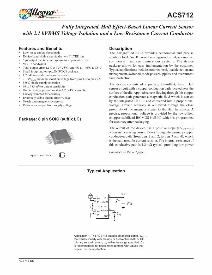
Approximate Scale 1:1
Application 1. The ACS712 outputs an analog signal, VOUT . that varies linearly with the uni- or bi-directional AC or DC primary sensed current, IP , within the range specified. CF is recommended for noise management, with values that depend on the application.
ACS712
DescriptionThe Allegro® ACS712 provides economical and precise solutions for AC or DC current sensing in industrial, automotive, commercial, and communications systems. The device package allows for easy implementation by the customer. Typical applications include motor control, load detection and management, switched-mode power supplies, and overcurrent fault protection.
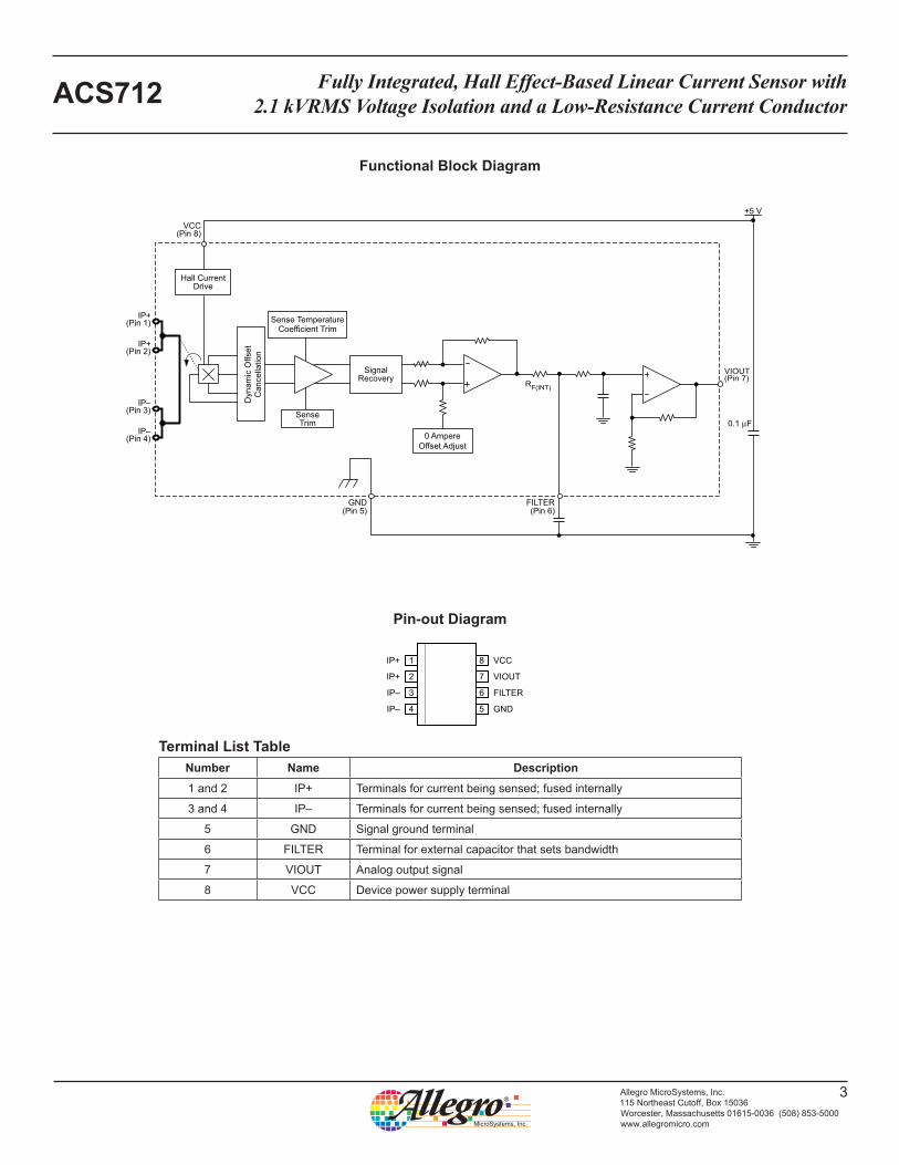
The device consists of a precise, low-offset, linear Hall sensor circuit with a copper conduction path located near the surface of the die. Applied current flowing through this copper conduction path generates a magnetic field which is sensed by the integrated Hall IC and converted into a proportional voltage. Device accuracy is optimized through the close proximity of the magnetic signal to the Hall transducer. A precise, proportional voltage is provided by the low-offset, chopper-stabilized BiCMOS Hall IC, which is programmed for accuracy after packaging.
The output of the device has a positive slope (>VIOUT(Q)) when an increasing current flows through the primary copper conduction path (from pins 1 and 2, to pins 3 and 4), which is the path used for current sensing. The internal resistance of this conductive path is 1.2 mΩ typical, providing low power
ACS712-DS
Features and Benefits Low-noise analog signal path Device bandwidth is set via the new FILTER pin 5 µs output rise time in response to step input current 50 kHz bandwidth Total output error 1.5% at TA = 25°C, and 4% at –40°C to 85°C Small footprint, low-profile SOIC8 package 1.2 mΩ internal conductor resistance 2.1 kVRMS minimum isolation voltage from pins 1-4 to pins 5-8 5.0 V, single supply operation 66 to 185 mV/A output sensitivity Output voltage proportional to AC or DC currents Factory-trimmed for accuracy Extremely stable output offset voltage Nearly zero magnetic hysteresis Ratiometric output from supply voltage
Fully Integrated, Hall Effect-Based Linear Current Sensor with 2.1 kVRMS Voltage Isolation and a Low-Resistance Current Conductor
Continued on the next page…
Package: 8 pin SOIC (suffix LC)
Typical Application
IP+IP+
IP–IP–
IP
5GND
2
4
1
3ACS712
7
8+5 V
VIOUTVOUT
6FILTER
VCC
CBYP0.1 µF
CF1 nF
Fully Integrated, Hall Effect-Based Linear Current Sensor with 2.1 kVRMS Voltage Isolation and a Low-Resistance Current ConductorACS712
2Allegro MicroSystems, Inc.115 Northeast Cutoff, Box 15036Worcester, Massachusetts 01615-0036 (508) 853-5000www.allegromicro.com
Selection Guide
Part Number Packing* TOP (°C)
Optimized Range, IP (A)
Sensitivity, Sens (Typ) (mV/A)
ACS712ELCTR-05B-T Tape and reel, 3000 pieces/reel –40 to 85 ±5 185
ACS712ELCTR-20A-T Tape and reel, 3000 pieces/reel –40 to 85 ±20 100
ACS712ELCTR-30A-T Tape and reel, 3000 pieces/reel –40 to 85 ±30 66
*Contact Allegro for additional packing options.
loss. The thickness of the copper conductor allows survival of the device at up to 5× overcurrent conditions. The terminals of the conductive path are electrically isolated from the sensor leads (pins 5 through 8). This allows the ACS712 current sensor to be used in applications requiring electrical isolation without the use of opto-isolators or other costly isolation techniques.
The ACS712 is provided in a small, surface mount SOIC8 package. The leadframe is plated with 100% matte tin, which is compatible with standard lead (Pb) free printed circuit board assembly processes. Internally, the device is Pb-free, except for flip-chip high-temperature Pb-based solder balls, currently exempt from RoHS. The device is fully calibrated prior to shipment from the factory.
Description (continued)
Absolute Maximum RatingsCharacteristic Symbol Notes Rating Units
Supply Voltage VCC 8 V
Reverse Supply Voltage VRCC –0.1 V
Output Voltage VIOUT 8 V
Reverse Output Voltage VRIOUT –0.1 V
Output Current Source IIOUT(Source) 3 mA
Output Current Sink IIOUT(Sink) 10 mA
Overcurrent Transient Tolerance IP100 total pulses, 250 ms duration each, applied at a rate of 1 pulse every 100 seconds. 60 A
Maximum Transient Sensed Current IR(max) Junction Temperature, TJ < TJ(max) 60 A
Nominal Operating Ambient Temperature TA Range E –40 to 85 ºC
Maximum Junction TJ(max) 165 ºC
Storage Temperature Tstg –65 to 170 ºC
TÜV America Certificate Number: U8V 06 05 54214 010
Parameter Specification
Fire and Electric ShockCAN/CSA-C22.2 No. 60950-1-03
UL 60950-1:2003EN 60950-1:2001
Fully Integrated, Hall Effect-Based Linear Current Sensor with 2.1 kVRMS Voltage Isolation and a Low-Resistance Current ConductorACS712
3Allegro MicroSystems, Inc.115 Northeast Cutoff, Box 15036Worcester, Massachusetts 01615-0036 (508) 853-5000www.allegromicro.com
VCC(Pin 8)
(Pin 7)VIOUT
RF(INT)
GND(Pin 5)
FILTER(Pin 6)
Dyn
amic
Offs
et
Can
cella
tion
IP+(Pin 1)
IP+(Pin 2)
IP–(Pin 3)
IP–(Pin 4)
SenseTrim
SignalRecovery
Sense TemperatureCoefficient Trim
0 AmpereOffset Adjust
Hall CurrentDrive
+5 V
IP+
IP+
IP–
IP–
VCC
VIOUT
FILTER
GND
1
2
3
4
8
7
6
5
Terminal List TableNumber Name Description
1 and 2 IP+ Terminals for current being sensed; fused internally
3 and 4 IP– Terminals for current being sensed; fused internally
5 GND Signal ground terminal
6 FILTER Terminal for external capacitor that sets bandwidth
7 VIOUT Analog output signal
8 VCC Device power supply terminal
Functional Block Diagram
Pin-out Diagram
Fully Integrated, Hall Effect-Based Linear Current Sensor with 2.1 kVRMS Voltage Isolation and a Low-Resistance Current ConductorACS712
4Allegro MicroSystems, Inc.115 Northeast Cutoff, Box 15036Worcester, Massachusetts 01615-0036 (508) 853-5000www.allegromicro.com
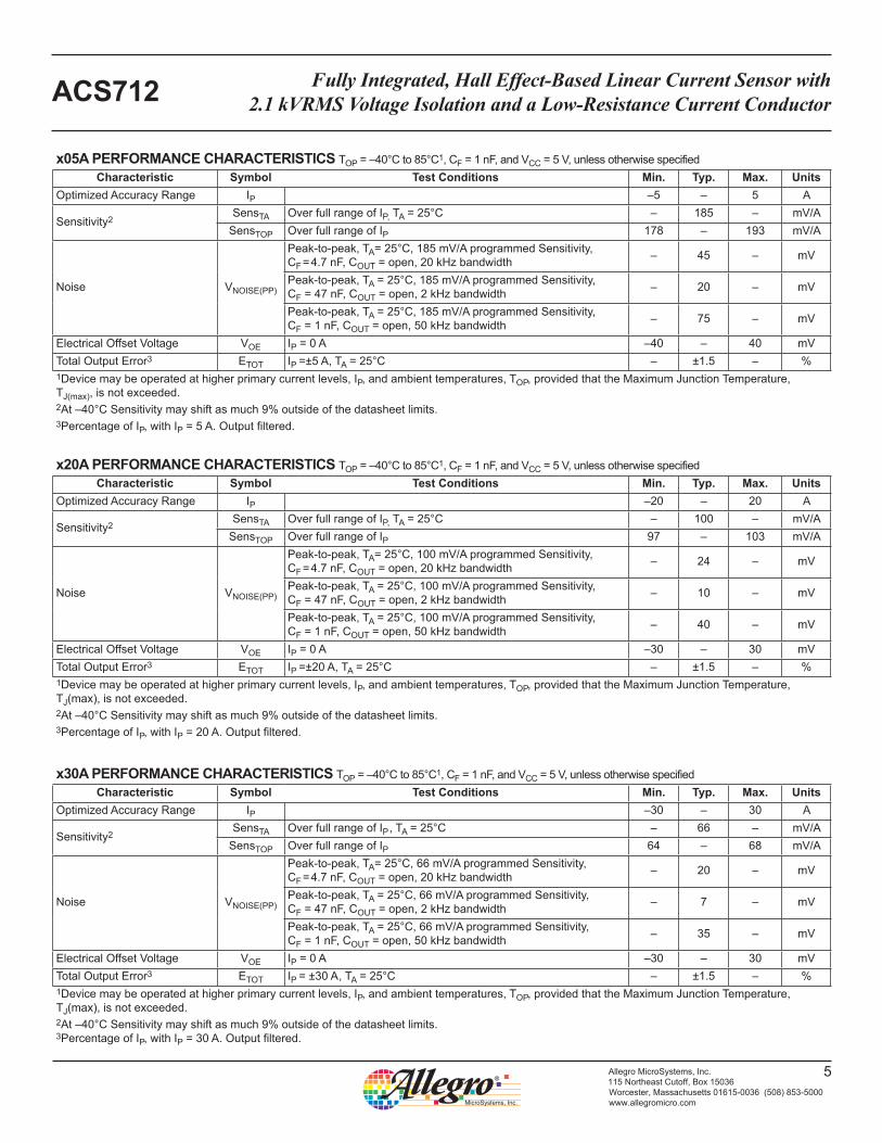
COMMON OPERATING CHARACTERISTICS1 over full range of TOP , CF = 1 nF, and VCC = 5 V, unless otherwise specifiedCharacteristic Symbol Test Conditions Min. Typ. Max. Units
ELECTRICAL CHARACTERISTICSSupply Voltage VCC 4.5 5.0 5.5 VSupply Current ICC VCC = 5.0 V, output open 6 8 11 mAOutput Zener Clamp Voltage VZ ICC = 11 mA, TA = 25°C 6 8.3 – VOutput Resistance RIOUT IIOUT = 1.2 mA, TA=25°C – 1 2 ΩOutput Capacitance Load CLOAD VIOUT to GND – – 10 nFOutput Resistive Load RLOAD VIOUT to GND 4.7 – – kΩPrimary Conductor Resistance RPRIMARY TA = 25°C – 1.2 – mΩRMS Isolation Voltage VISORMS Pins 1-4 and 5-8; 60 Hz, 1 minute, TA=25°C 2100 – – VDC Isolation Voltage VISODC Pins 1-4 and 5-8; 1 minute, TA=25°C – 5000 – VPropagation Time tPROP IP = IP(max), TA = 25°C, COUT = open – 3 – μsResponse Time tRESPONSE IP = IP(max), TA = 25°C, COUT = open – 7 – μsRise Time tr IP = IP(max), TA = 25°C, COUT = open – 5 – μsFrequency Bandwidth f –3 dB, TA = 25°C; IP is 10 A peak-to-peak 50 – – kHzNonlinearity ELIN Over full range of IP – ±1 ±1.5 %Symmetry ESYM Over full range of IP 98 100 102 %
Zero Current Output Voltage VIOUT(Q) Bidirectional; IP = 0 A, TA = 25°C – VCC × 0.5 – V
Magnetic Offset Error VERROM IP = 0 A, after excursion of 5 A – 0 – mV
Clamping VoltageVCH Typ. –110 VCC ×
0.9375 Typ. +110 mV
VCL Typ. –110 VCC × 0.0625 Typ. +110 mV
Power-On Time tPOOutput reaches 90% of steady-state level, TJ = 25°C, 20 A present on leadframe – 35 – µs
Magnetic Coupling2 – 12 – G/AInternal Filter Resistance3 RF(INT) 1.7 kΩ1Device may be operated at higher primary current levels, IP, and ambient, TA , and internal leadframe temperatures, TOP , provided that the Maximum Junction Temperature, TJ(max), is not exceeded.21G = 0.1 mT. 3RF(INT) forms an RC circuit via the FILTER pin.
COMMON THERMAL CHARACTERISTICS1
Min. Typ. Max. UnitsOperating Internal Leadframe Temperature TOP E range –40 – 85 °C
Value UnitsJunction-to-Lead Thermal Resistance2 RθJL Mounted on the Allegro ASEK 712 evaluation board 5 °C/W
Junction-to-Ambient Thermal Resistance RθJAMounted on the Allegro 85-0322 evaluation board, includes the power con-sumed by the board 23 °C/W
1Additional thermal information is available on the Allegro website.2The Allegro evaluation board has 1500 mm2 of 2 oz. copper on each side, connected to pins 1 and 2, and to pins 3 and 4, with thermal vias connect-ing the layers. Performance values include the power consumed by the PCB. Further details on the board are available from the Frequently Asked Questions document on our website. Further information about board design and thermal performance also can be found in the Applications Informa-tion section of this datasheet.
Fully Integrated, Hall Effect-Based Linear Current Sensor with 2.1 kVRMS Voltage Isolation and a Low-Resistance Current ConductorACS712
5Allegro MicroSystems, Inc.115 Northeast Cutoff, Box 15036Worcester, Massachusetts 01615-0036 (508) 853-5000www.allegromicro.com
x05A PERFORMANCE CHARACTERISTICS TOP = –40°C to 85°C1, CF = 1 nF, and VCC = 5 V, unless otherwise specifiedCharacteristic Symbol Test Conditions Min. Typ. Max. Units
Optimized Accuracy Range IP –5 – 5 A
Sensitivity2SensTA Over full range of IP, TA = 25°C – 185 – mV/A
SensTOP Over full range of IP 178 – 193 mV/A
Noise VNOISE(PP)
Peak-to-peak, TA= 25°C, 185 mV/A programmed Sensitivity, CF = 4.7 nF, COUT = open, 20 kHz bandwidth – 45 – mV
Peak-to-peak, TA = 25°C, 185 mV/A programmed Sensitivity, CF = 47 nF, COUT = open, 2 kHz bandwidth – 20 – mV
Peak-to-peak, TA = 25°C, 185 mV/A programmed Sensitivity, CF = 1 nF, COUT = open, 50 kHz bandwidth – 75 – mV
Electrical Offset Voltage VOE IP = 0 A –40 – 40 mVTotal Output Error3 ETOT IP =±5 A, TA = 25°C – ±1.5 – %1Device may be operated at higher primary current levels, IP, and ambient temperatures, TOP, provided that the Maximum Junction Temperature, TJ(max), is not exceeded.2At –40°C Sensitivity may shift as much 9% outside of the datasheet limits.3Percentage of IP, with IP = 5 A. Output filtered.
x20A PERFORMANCE CHARACTERISTICS TOP = –40°C to 85°C1, CF = 1 nF, and VCC = 5 V, unless otherwise specifiedCharacteristic Symbol Test Conditions Min. Typ. Max. Units
Optimized Accuracy Range IP –20 – 20 A
Sensitivity2SensTA Over full range of IP, TA = 25°C – 100 – mV/A
SensTOP Over full range of IP 97 – 103 mV/A
Noise VNOISE(PP)
Peak-to-peak, TA= 25°C, 100 mV/A programmed Sensitivity, CF = 4.7 nF, COUT = open, 20 kHz bandwidth – 24 – mV
Peak-to-peak, TA = 25°C, 100 mV/A programmed Sensitivity, CF = 47 nF, COUT = open, 2 kHz bandwidth – 10 – mV
Peak-to-peak, TA = 25°C, 100 mV/A programmed Sensitivity, CF = 1 nF, COUT = open, 50 kHz bandwidth – 40 – mV
Electrical Offset Voltage VOE IP = 0 A –30 – 30 mVTotal Output Error3 ETOT IP =±20 A, TA = 25°C – ±1.5 – %1Device may be operated at higher primary current levels, IP, and ambient temperatures, TOP, provided that the Maximum Junction Temperature, TJ(max), is not exceeded.2At –40°C Sensitivity may shift as much 9% outside of the datasheet limits.3Percentage of IP, with IP = 20 A. Output filtered.
x30A PERFORMANCE CHARACTERISTICS TOP = –40°C to 85°C1, CF = 1 nF, and VCC = 5 V, unless otherwise specifiedCharacteristic Symbol Test Conditions Min. Typ. Max. Units
Optimized Accuracy Range IP –30 – 30 A
Sensitivity2SensTA Over full range of IP , TA = 25°C – 66 – mV/A
SensTOP Over full range of IP 64 – 68 mV/A
Noise VNOISE(PP)
Peak-to-peak, TA= 25°C, 66 mV/A programmed Sensitivity, CF = 4.7 nF, COUT = open, 20 kHz bandwidth – 20 – mV
Peak-to-peak, TA = 25°C, 66 mV/A programmed Sensitivity, CF = 47 nF, COUT = open, 2 kHz bandwidth – 7 – mV
Peak-to-peak, TA = 25°C, 66 mV/A programmed Sensitivity, CF = 1 nF, COUT = open, 50 kHz bandwidth – 35 – mV
Electrical Offset Voltage VOE IP = 0 A –30 – 30 mVTotal Output Error3 ETOT IP = ±30 A , TA = 25°C – ±1.5 – %1Device may be operated at higher primary current levels, IP, and ambient temperatures, TOP, provided that the Maximum Junction Temperature, TJ(max), is not exceeded.2At –40°C Sensitivity may shift as much 9% outside of the datasheet limits. 3Percentage of IP, with IP = 30 A. Output filtered.
Fully Integrated, Hall Effect-Based Linear Current Sensor with 2.1 kVRMS Voltage Isolation and a Low-Resistance Current ConductorACS712
6Allegro MicroSystems, Inc.115 Northeast Cutoff, Box 15036Worcester, Massachusetts 01615-0036 (508) 853-5000www.allegromicro.com
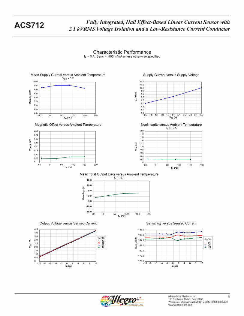
Characteristic PerformanceIP = 5 A, Sens = 185 mV/A unless otherwise specified
6.0
6.5
7.0
7.5
8.0
8.5
9.0
9.5
10.0
-50 0 50 100 150 200TA (°C)
TA (°C)
Mea
n I C
C (m
A) V
ERRO
M (m
V) V
IOUT
(V)
8.58.78.99.19.39.59.79.9
10.110.310.5
4.5 4.6 4.7 4.8 4.9 5 5.1 5.2 5.3 5.4 5.5VCC (V)
I CC
(mA
)E L
IN(%
)
TA (°C)-50 0 50 100 150 200
0
0.25
0.50
0.75
1.00
1.25
1.50
1.75
2.00
-50 0 50 100 150 200 00.20.40.60.81.01.21.41.61.82.0
TA (°C)
Mea
n E T
OT (
%)
-15.0
-10.0
-5.0
0.0
5.0
10.0
15.0
-50 0 50 100 150 200
00.51.01.52.02.53.03.54.04.5
-10 -8 -6 -4 -2 0 2 4 6 8 10Ip (A) Ip (A)
176.0
178.0
180.0
182.0
184.0
186.0
188.0
-10 -8 -6 -4 -2 0 2 4 6 8 10
Sens
(mV/
A)
-402585
150TA (°C)
-402585
TA (°C)
Mean Supply Current versus Ambient TemperatureVCC = 5 V
Supply Current versus Supply Voltage
Magnetic Offset versus Ambient Temperature Nonlinearity versus Ambient TemperatureIP = 10 A
Mean Total Output Error versus Ambient TemperatureIP = 10 A
Output Voltage versus Sensed Current Sensitivity versus Sensed Current
Fully Integrated, Hall Effect-Based Linear Current Sensor with 2.1 kVRMS Voltage Isolation and a Low-Resistance Current ConductorACS712
7Allegro MicroSystems, Inc.115 Northeast Cutoff, Box 15036Worcester, Massachusetts 01615-0036 (508) 853-5000www.allegromicro.com
-50 0 50 100 150 200TA (°C)
TA (°C)
Mea
n I C
C (m
A) V
ERRO
M (m
V) V
IOUT
(V)
8.58.78.99.19.39.59.79.9
10.110.310.5
4.5 4.6 4.7 4.8 4.9 5 5.1 5.2 5.3 5.4 5.5VCC (V)
I CC
(mA
)E L
IN(%
)
TA (°C)-50 0 50 100 150 200
0
0.20
0.40
0.60
0.80
1.00
-50 0 50 100 150 200 00.20.40.60.81.01.21.41.61.82.0
TA (°C)
Mea
n E
TOT (
%)
-5.0
-3.0-2.0
-4.0
-1.00.01.02.03.04.05.0
-50 0 50 100 150 200
00.51.01.52.02.53.03.54.04.5
-30 -20 -10 0 10 20 30 -30 -20 -10 0 10 20 30Ip (A) Ip (A)
50.0
55.0
60.0
65.0
70.0
75.0
Sens
(mV/
A)
-402585
150TA (°C)
-402585
TA (°C)
6.0
6.5
7.0
7.5
8.0
8.5
9.0
9.5
10.0
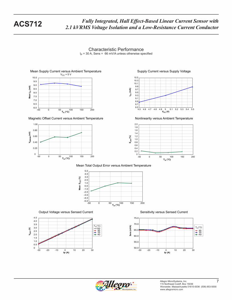
Mean Supply Current versus Ambient TemperatureVCC = 5 V
Supply Current versus Supply Voltage
Magnetic Offset Current versus Ambient Temperature Nonlinearity versus Ambient Temperature
Mean Total Output Error versus Ambient Temperature
Output Voltage versus Sensed Current Sensitivity versus Sensed Current
Characteristic PerformanceIP = 30 A, Sens = 66 mV/A unless otherwise specified
Fully Integrated, Hall Effect-Based Linear Current Sensor with 2.1 kVRMS Voltage Isolation and a Low-Resistance Current ConductorACS712
8Allegro MicroSystems, Inc.115 Northeast Cutoff, Box 15036Worcester, Massachusetts 01615-0036 (508) 853-5000www.allegromicro.com
Sensitivity (Sens). The change in sensor output in response to a 1 A change through the primary conductor. The sensitivity is the product of the magnetic circuit sensitivity (G / A) and the linear IC amplifier gain (mV/G). The linear IC amplifier gain is pro-grammed at the factory to optimize the sensitivity (mV/A) for the full-scale current of the device.
Noise (VNOISE). The product of the linear IC amplifier gain (mV/G) and the noise floor for the Allegro Hall effect linear IC (≈1 G). The noise floor is derived from the thermal and shot noise observed in Hall elements. Dividing the noise (mV) by the sensitivity (mV/A) provides the smallest current that the device is able to resolve.
Linearity (ELIN). The degree to which the voltage output from the sensor varies in direct proportion to the primary current through its full-scale amplitude. Nonlinearity in the output can be attributed to the saturation of the flux concentrator approaching the full-scale current. The following equation is used to derive the linearity:
where VIOUT_full-scale amperes = the output voltage (V) when the sensed current approximates full-scale ±IP .
Symmetry (ESYM). The degree to which the absolute voltage output from the sensor varies in proportion to either a positive or negative full-scale primary current. The following formula is used to derive symmetry:
Quiescent output voltage (VIOUT(Q)). The output of the sensor when the primary current is zero. For a unipolar supply voltage, it nominally remains at VCC ⁄ 2. Thus, VCC = 5 V translates into VIOUT(Q) = 2.5 V. Variation in VIOUT(Q) can be attributed to the resolution of the Allegro linear IC quiescent voltage trim and thermal drift.
Electrical offset voltage (VOE). The deviation of the device out-put from its ideal quiescent value of VCC / 2 due to nonmagnetic causes. To convert this voltage to amperes, divide by the device sensitivity, Sens.
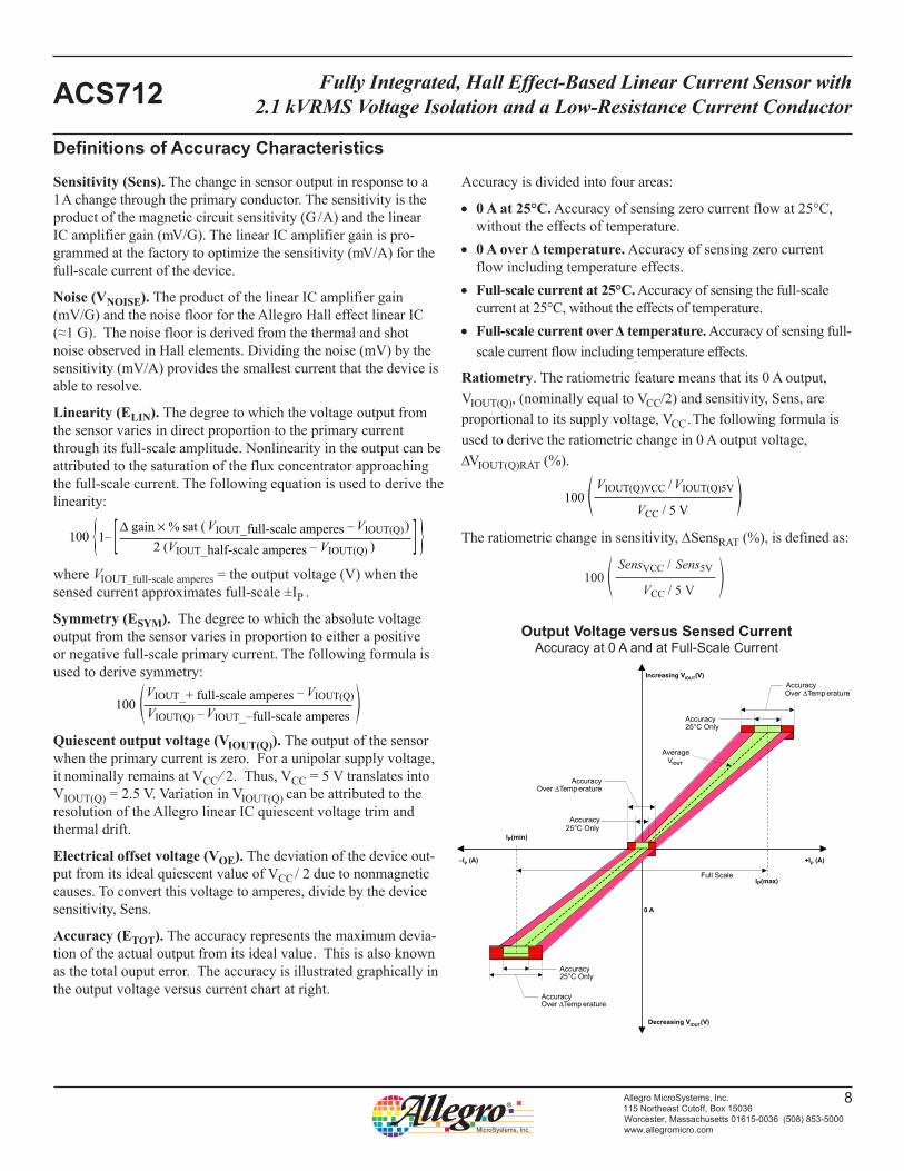
Accuracy (ETOT). The accuracy represents the maximum devia-tion of the actual output from its ideal value. This is also known as the total ouput error. The accuracy is illustrated graphically in the output voltage versus current chart at right.
Accuracy is divided into four areas:
• 0 A at 25°C. Accuracy of sensing zero current flow at 25°C, without the effects of temperature.
• 0 A over Δ temperature. Accuracy of sensing zero current flow including temperature effects.
• Full-scale current at 25°C. Accuracy of sensing the full-scale current at 25°C, without the effects of temperature.
• Full-scale current over Δ temperature. Accuracy of sensing full-scale current flow including temperature effects.
Ratiometry. The ratiometric feature means that its 0 A output, VIOUT(Q), (nominally equal to VCC/2) and sensitivity, Sens, are proportional to its supply voltage, VCC . The following formula is used to derive the ratiometric change in 0 A output voltage, ΔVIOUT(Q)RAT (%).
The ratiometric change in sensitivity, ΔSensRAT (%), is defined as:
Definitions of Accuracy Characteristics
100 1– [ [ VIOUT_full-scale amperes – VIOUT(Q)∆ gain × % sat ( )2 (VIOUT_half-scale amperes – VIOUT(Q) )
100VIOUT_+ full-scale amperes – VIOUT(Q)
VIOUT(Q) – VIOUT_–full-scale amperes
100VIOUT(Q)VCC / VIOUT(Q)5V
VCC / 5 V
100SensVCC / Sens5V
VCC / 5 V‰
Output Voltage versus Sensed CurrentAccuracy at 0 A and at Full-Scale Current
Increasing VIOUT(V)
+IP (A)
Accuracy
Accuracy
Accuracy25°C Only
Accuracy25°C Only
Accuracy25°C Only
Accuracy
0 A
v rO e Temp erature
AverageVIOUT
–IP (A)
v rO e Temp erature
v rO e Temp erature
Decreasing VIOUT(V)
IP(min)
IP(max)Full Scale
Fully Integrated, Hall Effect-Based Linear Current Sensor with 2.1 kVRMS Voltage Isolation and a Low-Resistance Current ConductorACS712
9Allegro MicroSystems, Inc.115 Northeast Cutoff, Box 15036Worcester, Massachusetts 01615-0036 (508) 853-5000www.allegromicro.com
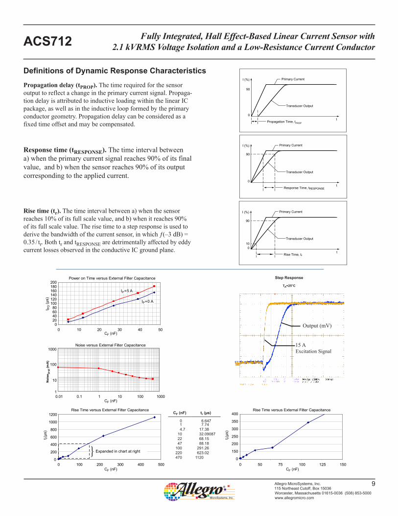
Rise Time versus External Filter Capacitance
0
200
400
600
800
1000
1200
0 100 200 300 400 500
t r(µs
)
Power on Time versus External Filter Capacitance
020406080
100120140160180200
0 10 20 30 40 50CF (nF)
CF (nF)
CF (nF)
Expanded in chart at right
Rise Time versus External Filter Capacitance
0
150
200
250
300
350
400
0 50 75 100 125 150
t r(µs
)
CF (nF)
t PO
(µs)
IP=5 A
IP=0 A
Noise versus External Filter Capacitance
1
100
10
1000
0.01 0.1 1 10 100 1000
Noi
se(p
-p)(
mA
)
Definitions of Dynamic Response Characteristics
Propagation delay (tPROP). The time required for the sensor output to reflect a change in the primary current signal. Propaga-tion delay is attributed to inductive loading within the linear IC package, as well as in the inductive loop formed by the primary conductor geometry. Propagation delay can be considered as a fixed time offset and may be compensated.
Primary Current
Transducer Output
90
0
I (%)
Propagation Time, tPROPt
Primary Current
Transducer Output
90
0
I (%)
Response Time, tRESPONSEt
Primary Current
Transducer Output
90
100
I (%)
Rise Time, trt
Rise time (tr). The time interval between a) when the sensor reaches 10% of its full scale value, and b) when it reaches 90% of its full scale value. The rise time to a step response is used to derive the bandwidth of the current sensor, in which ƒ(–3 dB) = 0.35 / tr. Both tr and tRESPONSE are detrimentally affected by eddy current losses observed in the conductive IC ground plane.
Response time (tRESPONSE). The time interval between a) when the primary current signal reaches 90% of its final value, and b) when the sensor reaches 90% of its output corresponding to the applied current.
Excitation Signal
Output (mV)
15 A
Step Response
TA=25°C
CF (nF) tr (µs)
0 6.647 1 7.74 4.7 17.38 10 32.09087 22 68.15 47 88.18 100 291.26 220 623.02 470 1120
Fully Integrated, Hall Effect-Based Linear Current Sensor with 2.1 kVRMS Voltage Isolation and a Low-Resistance Current ConductorACS712
10Allegro MicroSystems, Inc.115 Northeast Cutoff, Box 15036Worcester, Massachusetts 01615-0036 (508) 853-5000www.allegromicro.com
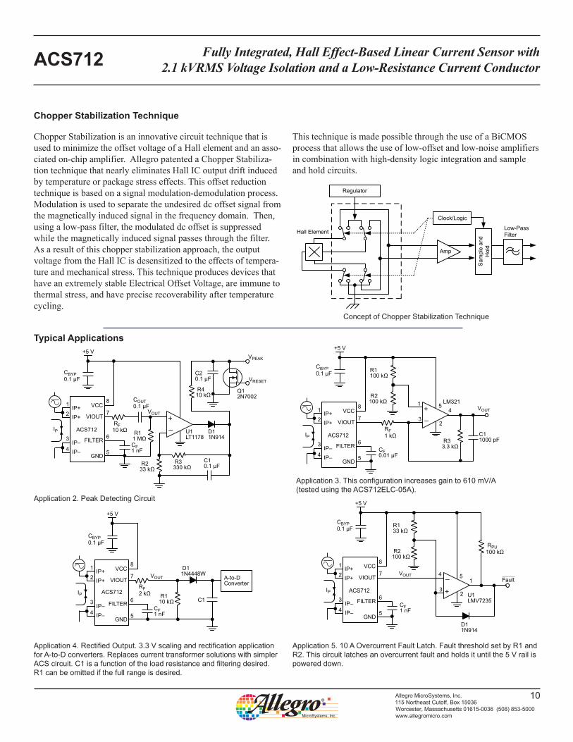
Chopper Stabilization is an innovative circuit technique that is used to minimize the offset voltage of a Hall element and an asso-ciated on-chip amplifier. Allegro patented a Chopper Stabiliza-tion technique that nearly eliminates Hall IC output drift induced by temperature or package stress effects. This offset reduction technique is based on a signal modulation-demodulation process. Modulation is used to separate the undesired dc offset signal from the magnetically induced signal in the frequency domain. Then, using a low-pass filter, the modulated dc offset is suppressed while the magnetically induced signal passes through the filter. As a result of this chopper stabilization approach, the output voltage from the Hall IC is desensitized to the effects of tempera-ture and mechanical stress. This technique produces devices that have an extremely stable Electrical Offset Voltage, are immune to thermal stress, and have precise recoverability after temperature cycling.
This technique is made possible through the use of a BiCMOS process that allows the use of low-offset and low-noise amplifiers in combination with high-density logic integration and sample and hold circuits.
Chopper Stabilization Technique
Amp
Regulator
Clock/Logic
Hall Element
Sam
ple
and
Hol
d
Low-PassFilter
Concept of Chopper Stabilization Technique
+
–IP+IP+
IP–IP–
IP
7
5
5
8
+5 V
U1LMV7235
VIOUTVOUT
GND
6
2
4
41
1
23
3
FILTER
VCC
ACS712
D11N914
R2100 kΩ
R133 kΩ
RPU100 kΩ
Fault
CBYP0.1 µF
CF1 nF
+
–
IP+IP+
IP–IP–
7
5
8
+5 V
U1LT1178
Q12N7002
VIOUTVOUT
VPEAK
VRESET
GND
6
2
4
1
3D11N914
VCC
ACS712
R410 kΩ
R11 MΩ
R233 kΩ
RF10 kΩ
R3330 kΩ
CBYP0.1 µF
C10.1 µF
COUT0.1 µF
CF1 nF
C20.1 µF
FILTER
IP
IP+IP+
IP–IP–
IP
7
5
8
+5 V
D11N4448W
VIOUTVOUT
GND
6
2
4
1
3 FILTER
VCC
ACS712 R110 kΩ
CBYP0.1 µF
RF2 kΩ
CF1 nF
C1
A-to-DConverter
Typical Applications
Application 5. 10 A Overcurrent Fault Latch. Fault threshold set by R1 and R2. This circuit latches an overcurrent fault and holds it until the 5 V rail is powered down.
Application 2. Peak Detecting Circuit
Application 4. Rectified Output. 3.3 V scaling and rectification application for A-to-D converters. Replaces current transformer solutions with simpler ACS circuit. C1 is a function of the load resistance and filtering desired. R1 can be omitted if the full range is desired.
+
–IP+IP+
IP–IP–
IP
7
5
58
+5 V
LM321
VIOUT
VOUT
GND
6
2
4
11 4
2
3
3
FILTER
VCC
ACS712
R2100 kΩ
R1100 kΩ
R33.3 kΩ
CBYP0.1 µF
CF0.01 µF
C11000 pF
RF1 kΩ
Application 3. This configuration increases gain to 610 mV/A (tested using the ACS712ELC-05A).
Fully Integrated, Hall Effect-Based Linear Current Sensor with 2.1 kVRMS Voltage Isolation and a Low-Resistance Current ConductorACS712
11Allegro MicroSystems, Inc.115 Northeast Cutoff, Box 15036Worcester, Massachusetts 01615-0036 (508) 853-5000www.allegromicro.com
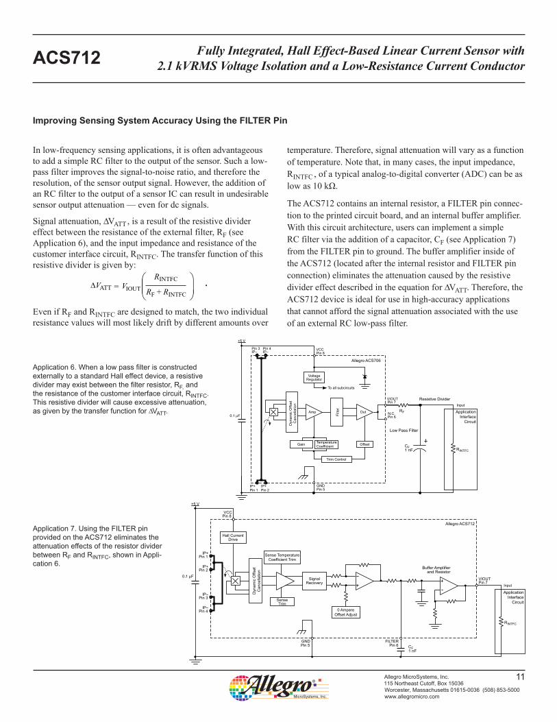
Improving Sensing System Accuracy Using the FILTER Pin
In low-frequency sensing applications, it is often advantageous to add a simple RC filter to the output of the sensor. Such a low-pass filter improves the signal-to-noise ratio, and therefore the resolution, of the sensor output signal. However, the addition of an RC filter to the output of a sensor IC can result in undesirable sensor output attenuation — even for dc signals.
Signal attenuation, ∆VATT , is a result of the resistive divider effect between the resistance of the external filter, RF (see Application 6), and the input impedance and resistance of the customer interface circuit, RINTFC. The transfer function of this resistive divider is given by:
Even if RF and RINTFC are designed to match, the two individual resistance values will most likely drift by different amounts over
temperature. Therefore, signal attenuation will vary as a function of temperature. Note that, in many cases, the input impedance, RINTFC , of a typical analog-to-digital converter (ADC) can be as low as 10 kΩ.
The ACS712 contains an internal resistor, a FILTER pin connec-tion to the printed circuit board, and an internal buffer amplifier. With this circuit architecture, users can implement a simple RC filter via the addition of a capacitor, CF (see Application 7) from the FILTER pin to ground. The buffer amplifier inside of the ACS712 (located after the internal resistor and FILTER pin connection) eliminates the attenuation caused by the resistive divider effect described in the equation for ∆VATT. Therefore, the ACS712 device is ideal for use in high-accuracy applications that cannot afford the signal attenuation associated with the use of an external RC low-pass filter.
=∆VATTRINTFC
RF + RINTFCVIOUT
.
Application 6. When a low pass filter is constructed externally to a standard Hall effect device, a resistive divider may exist between the filter resistor, RF, and the resistance of the customer interface circuit, RINTFC. This resistive divider will cause excessive attenuation, as given by the transfer function for ∆VATT.
Application 7. Using the FILTER pin provided on the ACS712 eliminates the attenuation effects of the resistor divider between RF and RINTFC, shown in Appli-cation 6.
ApplicationInterface
Circuit
Resistive Divider
RINTFC
Low Pass Filter
RFAmp Out
VCC
+5 V
Pin 8
Pin 7VIOUT
Pin 6N.C.
Input
GNDPin 5
Filte
r
Dyn
amic
Offs
et
Can
cella
tion
IP+ IP+
0.1 F
Pin 1 Pin 2
IP– IP–Pin 3 Pin 4
Gain TemperatureCoefficient Offset
VoltageRegulator
Trim Control
To all subcircuits
Input
VCCPin 8
Pin 7VIOUT
GNDPin 5
FILTERPin 6
Dyn
amic
Offs
etC
ance
llatio
n
IP+Pin 1
IP+Pin 2
IP–Pin 3
IP–Pin 4
SenseTrim
SignalRecovery
Sense TemperatureCoefficient Trim
0 AmpereOffset Adjust
Hall CurrentDrive
+5 V
ApplicationInterface
Circuit
Buffer Amplifier and Resistor
RINTFC
Allegro ACS712
Allegro ACS706
CF1 nF
CF1 nF
Fully Integrated, Hall Effect-Based Linear Current Sensor with 2.1 kVRMS Voltage Isolation and a Low-Resistance Current ConductorACS712
12Allegro MicroSystems, Inc.115 Northeast Cutoff, Box 15036Worcester, Massachusetts 01615-0036 (508) 853-5000www.allegromicro.com
The products described herein are manufactured under one or more of the following U.S. patents: 5,045,920; 5,264,783; 5,442,283; 5,389,889; 5,581,179; 5,517,112; 5,619,137; 5,621,319; 5,650,719; 5,686,894; 5,694,038; 5,729,130; 5,917,320; and other patents pending.Allegro MicroSystems, Inc. reserves the right to make, from time to time, such departures from the detail specifications as may be required to permit improvements in the performance, reliability,
or manufacturability of its products. Before placing an order, the user is cautioned to verify that the information being relied upon is current. The information included herein is believed to be accurate and reliable. However, Allegro MicroSystems, Inc. assumes no responsibility for its use; nor for any infringement of patents or other rights of third parties which may result from its use.Copyright ©2006, Allegro MicroSystems, Inc.
0.250.10
.010
.004
1.751.35
.069
.0530.510.31
.020
.012
4.00 3.80
.157 .150
0.250.17
.010
.007
8º0º
1.270.40
.050
.016
5.00 4.80
.197
.189
CSEATINGPLANE
AB
8X
0.25 [.010] M C A B
6.205.80
.244
.228
C0.10 [.004]8X
0.25 [.010] M B M
1.27 .050
0.25 .010
21
8
GAUGE PLANESEATING PLANE
Preliminary dimensions, for reference onlyDimensions in millimetersU.S. Customary dimensions (in.) in brackets, for reference only(reference JEDEC MS-012 AA)Dimensions exclusive of mold flash, gate burrs, and dambar protrusionsExact case and lead configuration at supplier discretion within limits shown
A Terminal #1 mark areaA
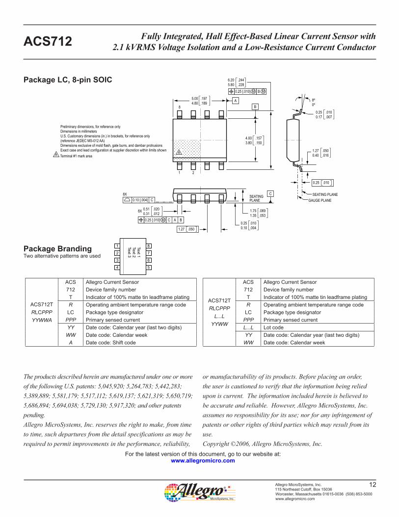
Package LC, 8-pin SOIC
ACS712T RLCPPP YYWWA
ACS Allegro Current Sensor712 Device family numberT Indicator of 100% matte tin leadframe platingR Operating ambient temperature range code
LC Package type designatorPPP Primary sensed currentYY Date code: Calendar year (last two digits)
WW Date code: Calendar weekA Date code: Shift code
ACS712T RLCPPP
L...L YYWW
ACS Allegro Current Sensor712 Device family numberT Indicator of 100% matte tin leadframe platingR Operating ambient temperature range code
LC Package type designatorPPP Primary sensed currentL...L Lot codeYY Date code: Calendar year (last two digits)
WW Date code: Calendar week
Package BrandingTwo alternative patterns are used
Text 1Text 2Text 3
1
2
3
4
8
7
6
5
For the latest version of this document, go to our website at:www.allegromicro.com