Embed Size (px)
Citation preview
FN8204Rev 0.00
March 8, 2005
X9470RF Power Amplifier (PA) Bias Controller
DATASHEETNOT RECOMMENDED FOR NEW DESIGNSNO RECOMMENDED REPLACEMENT
contact our Technical Support Center at1-888-INTERSIL or www.intersil.com/tsc
FEATURES
• Programmable Bias Controller IC for Class A and AB LDMOS Power Amplifiers
• Adaptive System on Chip Solution• Bias Current Calibration to better than ±4%
using Reference Trim DCP• Automatic Bias Point Tracking and Calibration
— IDQ Sensing and Tracking—Programmable Instrumentation Amplifier to
Scale Wide Range of IDQ —Programmable Gate Bias Driver—All Programmable settings are Nonvolatile—All Settings Recalled at Power-up.
• 28V Maximum VDD• 2 Wire Interface for Programming Bias Setting
and Optimizing IDQ Set Point• Bias Level Comparator• Shutdown Control pin for PA Signal• Slave address to allow for multiple devices• 24-pin TSSOP Package• Applications: Cellular Base Stations (GSM,
UMTS, CDMA, EDGE), TDD applications, Point-to-multipoint, and other RF power transmission systems
DESCRIPTION
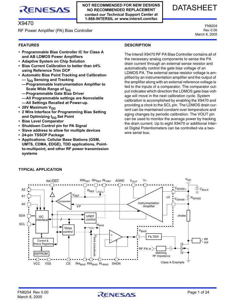
The Intersil X9470 RF PA Bias Controller contains all of the necessary analog components to sense the PA drain current through an external sense resistor and automatically control the gate bias voltage of an LDMOS PA. The external sense resistor voltage is am-plified by an instrumentation amplifier and the output of the amplifier along with an external reference voltage is fed to the inputs of a comparator. The comparator out-put indicates which direction the LDMOS gate bias volt-age will move in the next calibration cycle. System calibration is accomplished by enabling the X9470 and providing a clock to the SCL pin. The LDMOS drain cur-rent can be maintained constant over temperature and aging changes by periodic calibration. The VOUT pin can be used to monitor the average power by tracking the drain current. Up to eight X9470 or additional Inter-sil Digital Potentiometers can be controlled via a two-wire serial bus.
TYPICAL APPLICATION
A0
A2
VCC VSS
V+AGND
Comparator
choke
RF PA in
RSENSE
VDD
VREF
VSENSE+
VBIAS
INC/DEC
InstrumentationAmplifier
V
CS
VOUT
VSENSE–
RREF
RWREF RLREF
SHDN
+
–
EEPROM
SCL
SDA
A1
Vbiascontrol
VREFcontrol
I2Cinterface
Control & Status Registers
RFout
RHREF
RBIAS
VP
RHBIAS RLBIASRWBIAS
FILTER
VB
IAS
(Unbuffered) RF Impedance
Matching
CBULK
Class A Example
FN8204 Rev 0.00 Page 1 of 24March 8, 2005

X9470
PIN CONFIGURATION
ORDERING INFORMATION
PIN DESCRIPTIONS
Part Number Temperature Range Package
X9470V24I -40°C TO 85°C 24-Lead TSSOP
TSSOP pin Symbol Brief Description
1 VSENSE+ Positive sense voltage input terminal
2 RHREF Upper Terminal of Potentiometer, called the RREF potentiometer. The voltage applied to this pin will determine the upper voltage limit of the adjustment for the Up/Down threshold of the comparator.
3 RLREF Lower Terminal of Potentiometer, called the RREF potentiometer. The voltage applied to this pin will determine the lower voltage limit of the adjustment for the Up/Down threshold of the comparator.
4 RWREF Wiper Terminal of Potentiometer, called the RREF potentiometer. The voltage on this pin will be the threshold for the Up/Down comparator. Also referred to as the VREF of the comparator.
5 AGND Analog ground to allow single point grounding external to the package to minimize digital noise.
6 VSS System (Digital) Ground Reference
7 CS Chip Select. This input enables bias calibration adjustments to the RBIAS potentiometer. CMOS input with in-ternal pull-down.
8 SCL Dual function. Function 1: The increment control input. Increments or decrements the RBIAS potentiometer. Function 2: Serial Data Clock Input. Requires external pull-up.
9 SDA Serial Data Input. Bi-directional 2-wire interface. Requires external pull-up.
10 RHBIAS Upper Terminal of Potentiometer, called the RBIAS potentiometer. The voltage applied to this pin will determine the upper limit of the bias voltage to the PA (or VBIAS pin).
11 RWBIAS Wiper Terminal of Potentiometer, called the RBIAS potentiometer. This voltage is the equivalent to the unbuff-ered voltage that will appear at the VBIAS pin.
12 RLBIAS Lower Terminal of Potentiometer, called the RBIAS potentiometer. The voltage applied to this pin will determine the lower limit of the bias voltage to the PA (or VBIAS pin).
13 A0 External address pin which allows for a hardware slave address selection of this device. This pin has an internal pull-down.
14 A1 External address pin which allows for a hardware slave address selection of this device. This pin has an internal pull-down.
15 A2 External address pin which allows for a hardware slave address selection of this device. This pin has an internal pull-down.
16 VSS System (Digital) Ground Reference
17 VBIAS This is the bias output voltage pin and is used to drive the filter network to the PA gate.
18 VCC System (Digital) Supply Voltage
19 VCC System (Digital) Supply Voltage
20 V + Positive voltage supply for the instrumentation amplifier and other analog circuits.
21 VOUT Instrumentation Amplifier output that is 20x or 50x the voltage across the Rsense pins.
22 INC/DEC Status output that indicates the state of the comparator. When this pin is HIGH, the RBIAS potentiometer will increment; when the pin is LOW, the RBIAS potentiometer will decrement. This pin is open drain and requires external resistor pull-up.
23 SHDN Shutdown the output op amp. When SHDN is active (HIGH), the VBIAS pin is pulled LOW.
24 VSENSE- Negative sense voltage Input terminal
VOUTRWREF
V+
TSSOP
1
23
45
67
14
20
19
18
17
16
15
X9470
Vsense+ Vsense-
RHREFRLREF
VSS
AGND
SHDN
INC/DEC
VCC
A2RHBIAS
VCC
SDA
SCL VBIASVSS
CS
8
910
13RLBIAS
RWBIAS 1112 A0
A1
2423
22
21
FN8204 Rev 0.00 Page 2 of 24March 8, 2005

X9470
ABSOLUTE MAXIMUM RATINGS*
Voltage on V+ (referenced to AGND) ......................7VVoltage on VCC (reference to VSS) ........................7VVoltage on all RH, RW, RL pins
(reference to AGND): ...........................................7V Voltage on Vsense+ or
Vsense- (reference to AGRND)..........................30VVoltage on SDA, CS, SCL, SHDN
(reference to AGND) ............... -0.3V to (Vcc + 0.3V)Current into Output Pin: 5mAContinuous Power Dissipation: .......................500mWOperating Temperature range:.............. -40C to +85CJunction Temperature: ..........................................150CStorage Temperature ........................ -65C to +150CLead Temperature (Soldering, 10 seconds): ..... 300C
*COMMENT
Stresses above those listed under “Absolute MaximumRatings” may cause permanent damage to the device.This is a stress rating only and the functional operationof the device at these or any other conditions abovethose listed in the operational sections of this specifica-tion is not implied. Exposure to absolute maximum ratingconditions for extended periods may affect device reli-ability.
ELECTRICAL CHARACTERISTICSINSTRUMENTATION AMPLIFIERRecommended Operating Conditions: (Vcc, V+ = 4.75 to 5.25V; Vsense+, Vsense- = 26V; TA = -40°C to +85°C, unlessotherwise noted.)
Symbol Parameter
Limits
Test Conditions/NotesMin. Typ. Max. Units
VIN(10) Common Mode Input Voltage on
VSENSE+ and VSENSE- pins20 28 V
Gain 1 Gain from VSENSE to VOUT(2) 20 V/V Measured with Status
Register bit SR0 = 0
Gain 2 Gain from VSENSE to VOUT(2) 50 V/V Measured with Status
Register bit SR0 = 1
VRANGE1 Differential voltage sense range between VSENSE+ and VSENSE- for gain 1
60 90 mV Gain = 20
VRANGE2 Differential voltage sense range between VSENSE+ and VSENSE- for gain 2
40 60 mV Gain = 50
VOS Input Offset Voltage 0.5 mV VSENSE = 40mV to 90mV TA = 25°C
Av1 Gain 1 ErrorGain = 20 (4)
1.5 % VSENSE = 60mV to 90mV TA = 25 to 85°C, Gain = 20
Av2 Gain 2 ErrorGain = 50 (4)
1.5 % VSENSE = 40mV to 60mV TA = 25 to 85°C, Gain = 50
Avt1 Total Error, Gain 1Gain = 20 (5)
-6 1.5 6 % VSENSE = 60mV to 90mV TA = 85°C, Gain = 20
10 % VSENSE = 60mV to 90mV TA = 25 to 85°C, Gain = 20
Avt2 Total Error, Gain 2Gain = 50 (5)
-6 1.5 6 % VSENSE = 40mV to 60mV TA = 85°C, Gain = 50
10 % VSENSE = 40mV to 60mV TA = 25 to 85°C, Gain = 50
At Long Term Drift 2 % Avt1 or Avt2
SR(10) Slew Rate of Instrumentation Amp 0.2 V/µS VSENSE = 20mV step, Cout = 10pF Measured at VOUT
(1,3)
FN8204 Rev 0.00 Page 3 of 24March 8, 2005

X9470
COMPARATORRecommended Operating Conditions: (Vcc, V+ = 4.75 to 5.25V; Vsense+, Vsense- = 26V; TA = -40°C to +85°C, unless otherwise noted.)
Tsettle(10) Setting time of Instrumentation Amp 5.0 µS VSENSE = 20mV step, Cout =
10pF, settling to 1% of final valueMeasured at VOUT
(1,3)
CMRR Common Mode Rejection Ratio 40 dB For both Gain 1 and Gain 2
PSRR Power Supply Rejection Ratio 55 dB For both Gain 1 and Gain 2
VOUT Range VOUT Voltage Swing 0.3 1.8 V Gain = 20
0.3 3.0 V Gain = 50
VOUT Noise(10)
VOUT Voltage Noise, rms 3 mV Gain = 20
IVSENSE(10) VSENSE+, VSENSE- Input Bias
Current250 µA TA = 25°C
CVSENSE(10) VSENSE+, VSENSE- Input
Capacitance10 pF Each Input
Symbol Parameter
Limits
Test Conditions/NotesMin. Typ. Max. Units
VOL Output Voltage Low on the INC/DEC pin 0.4 V IOL = 1mA
Io(10) Output sink Current 3 mA INC/DEC pin, open drain
Vos(10) Input Hysteresis 20 mV Vcc = 5 V
Tpd(10) Response Time for propagation delay 2 S INC/DEC pin with 2k pull up
ELECTRICAL CHARACTERISTICSINSTRUMENTATION AMPLIFIER (CONTINUED)
Recommended Operating Conditions: (Vcc, V+ = 4.75 to 5.25V; Vsense+, Vsense- = 26V; TA = -40°C to +85°C, unlessotherwise noted.)
Symbol Parameter
Limits
Test Conditions/NotesMin. Typ. Max. Units
VREF DCP CIRCUIT BLOCKRecommended Operating Conditions: (Vcc, V+ = 4.75 to 5.25V; Vsense+, Vsense- = 26V; TA = -40°C to +85°C, unlessotherwise noted.)
Symbol Parameter
Limits
Test Conditions/NotesMin. Typ. Max. Units
RTOTAL End to End Resistance 8 10 12 k
Number Taps or Positions 64
VRH RHREF Terminal Voltage AGND V+ V AGND = 0V
VRL RLREF Terminal Voltage AGND V+ V AGND = 0V
VRW RWREF Terminal Voltage AGND V+ V AGND = 0V
Power Rating(10) 2.5 mW RTOTAL 10k
Resolution(10) 1.6 %
Absolute Linearity(6) -0.2 +0.2 MI(8)
Relative Linearity(7) -0.2 +0.2 MI(8)
FN8204 Rev 0.00 Page 4 of 24March 8, 2005

X9470
BIAS ADJUSTMENT DCP CIRCUIT BLOCKRecommended Operating Conditions: (Vcc, V+ = 4.75 to 5.25V; Vsense+, Vsense- = 26V; TA = -40°C to +85°C, unless otherwise noted.)
RTOTAL Temperature Coefficient(10) ±300 ppm/°C
Ratiometric Temperature Coefficient(10) -20 +20 ppm/°C
CIN(10) Potentiometer Capacitances on RHREF
and RLREF
10 pF
Symbol Parameter
Limits
Test Conditions/NotesMin. Typ. Max. Units
RTOTAL End to End Resistance Variation 8 10 12 k with ±20% variation
Number Taps or Positions 256
VRH Voltage at the RHBIAS Terminal Voltage AGND V+ V AGND = 0V
VRL Voltage at the RLBIAS Terminal Voltage AGND V+ V AGND = 0V
VRW Voltage at the RWBIAS Terminal Voltage AGND V+ V AGND = 0V
Power Rating(10) 2.5 mW RTOTAL 10 K
Resolution(10) 0.4 %
Absolute Linearity(6) -1.0 +1.0 MI(8)
Relative Linearity(7) -1.0 +1.0 MI(8)
RTOTAL Temperature Coefficient(10) ±300 ppm/°C
Ratiometric Temperature Coefficient(10) -50 50 ppm/°C
CIN(10) Potentiometer Capacitances on RHBIAS
and RLBIAS
10 pF
VREF DCP CIRCUIT BLOCKRecommended Operating Conditions: (Vcc, V+ = 4.75 to 5.25V; Vsense+, Vsense- = 26V; TA = -40°C to +85°C, unlessotherwise noted.)
Symbol Parameter
Limits
Test Conditions/NotesMin. Typ. Max. Units
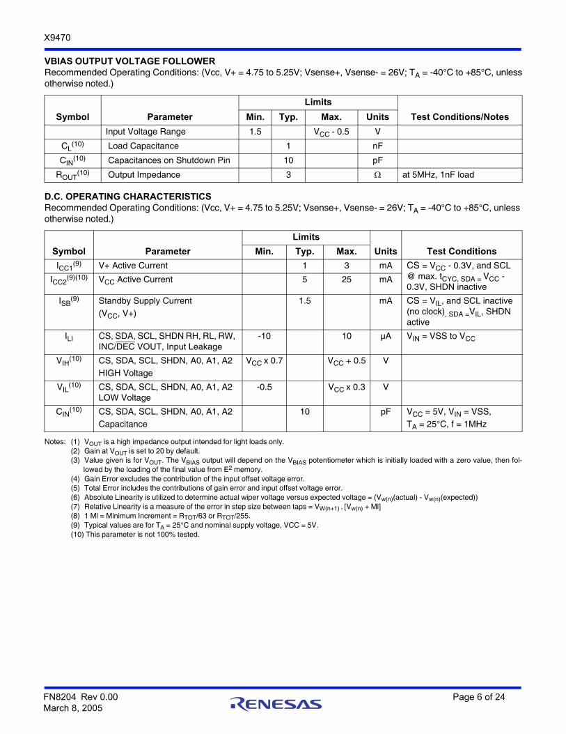
VBIAS OUTPUT VOLTAGE FOLLOWERRecommended Operating Conditions: (Vcc, V+ = 4.75 to 5.25V; Vsense+, Vsense- = 26V; TA = -40°C to +85°C, unlessotherwise noted.)
Symbol Parameter
Limits
Test Conditions/NotesMin. Typ. Max. Units
VOS Input Offset Voltage 10 mV
VOSDRIFT(10) Offset Voltage Temperature
Coefficient10 µV/°C TA = -40 to +85°C
SR Output Slew Rate on VBIAS 0.5 V/S RL = 10k, 1nF, VBIAS = 20mV
VBIAS Voltage Output Swing 1.5 VCC - 0.5 V IOUT = ±10mA
TS(10) Settling Time 2 µs Final value ±1%, RL = 10k,
1nF, VBIAS = 20mV
tSHDN Time for SHDN pin (delay) valid 0.1 1.0 µs
PSRR Power Supply Rejection Ratio 45 55 dB VCC supply VCC = 4.75 to 5.25V
FN8204 Rev 0.00 Page 5 of 24March 8, 2005
X9470
D.C. OPERATING CHARACTERISTICSRecommended Operating Conditions: (Vcc, V+ = 4.75 to 5.25V; Vsense+, Vsense- = 26V; TA = -40°C to +85°C, unless otherwise noted.)
Notes: (1) VOUT is a high impedance output intended for light loads only.(2) Gain at VOUT is set to 20 by default.(3) Value given is for VOUT. The VBIAS output will depend on the VBIAS potentiometer which is initially loaded with a zero value, then fol-
lowed by the loading of the final value from E2 memory.(4) Gain Error excludes the contribution of the input offset voltage error.(5) Total Error includes the contributions of gain error and input offset voltage error.(6) Absolute Linearity is utilized to determine actual wiper voltage versus expected voltage = (Vw(n)(actual) - Vw(n)(expected))(7) Relative Linearity is a measure of the error in step size between taps = VW(n+1) - [Vw(n) + Ml] (8) 1 Ml = Minimum Increment = RTOT/63 or RTOT/255.(9) Typical values are for TA = 25°C and nominal supply voltage, VCC = 5V.(10) This parameter is not 100% tested.
Input Voltage Range 1.5 VCC - 0.5 V
CL(10) Load Capacitance 1 nF
CIN(10) Capacitances on Shutdown Pin 10 pF
ROUT(10) Output Impedance 3 at 5MHz, 1nF load
Symbol Parameter
Limits
Units Test ConditionsMin. Typ. Max.
ICC1(9) V+ Active Current 1 3 mA CS = VCC - 0.3V, and SCL
@ max. tCYC, SDA = VCC - 0.3V, SHDN inactive
ICC2(9)(10) VCC Active Current 5 25 mA
ISB(9) Standby Supply Current
(VCC, V+)1.5 mA CS = VIL, and SCL inactive
(no clock), SDA =VIL, SHDN active
ILI CS, SDA, SCL, SHDN RH, RL, RW, INC/DEC VOUT, Input Leakage
-10 10 µA VIN = VSS to VCC
VIH(10) CS, SDA, SCL, SHDN, A0, A1, A2
HIGH VoltageVCC x 0.7 VCC + 0.5 V
VIL(10) CS, SDA, SCL, SHDN, A0, A1, A2
LOW Voltage-0.5 VCC x 0.3 V
CIN(10) CS, SDA, SCL, SHDN, A0, A1, A2
Capacitance10 pF VCC = 5V, VIN = VSS,
TA = 25°C, f = 1MHz
VBIAS OUTPUT VOLTAGE FOLLOWERRecommended Operating Conditions: (Vcc, V+ = 4.75 to 5.25V; Vsense+, Vsense- = 26V; TA = -40°C to +85°C, unlessotherwise noted.)
Symbol Parameter
Limits
Test Conditions/NotesMin. Typ. Max. Units
FN8204 Rev 0.00 Page 6 of 24March 8, 2005

X9470
BIAS ADJUSTMENT CIRCUIT BLOCK
A.C. OPERATING CHARACTERISTICS Recommended Operating Conditions: (Vcc, V+ = 4.75 to 5.25V; Vsense+, Vsense- = 26V; TA = -40°C to +85°C, unless otherwise noted.)
A.C. TIMING
Note: (11) MI in the A.C. timing diagram refers to the minimum incremental change in the VBIAS output due to a change in the wiper position.
Symbol Parameter
Limits
UnitsMin. Typ.(9) Max.
tCl CS to SCL Setup 100 ns
tlD Vsense Change to INC/DEC Change 5 s
tlL SCL LOW Period 1.5 s
tlH SCL HIGH Period 1.5 s
tlC(10) SCL Inactive to CS Inactive 100 ns
tIW(10)(11) SCL to VBIAS Change 3 s
tCYC SCL Cycle Time 3 s
tR, tF(10) SCL Input Rise and Fall Time 500 ns
CS
SCL
INC/DEC
VBIAS
tCI tIL tIH
tCYC
tID
tIW
tIC
tF tR
10%90% 90%
(Vsense+ – Vsense-)
FN8204 Rev 0.00 Page 7 of 24March 8, 2005

X9470
AC SPECIFICATIONS
Note: (12) Cb = total capacitance of one bus line in pF.
TIMING DIAGRAMS
Bus Timing
Write Cycle Timing
Symbol Parameter Min. Max. Unit
fSCL SCL Clock Frequency 0 400 kHz
tIN(10) Pulse width Suppression Time at inputs 50 ns
tAA(10) SCL LOW to SDA Data Out Valid 0.1 0.9 µs
tBUF(10) Time the bus must be free before a new transmission can start 1.3 µs
tLOW Clock LOW Time 1.3 µs
tHIGH Clock HIGH Time 0.6 µs
tSU:STA Start Condition Setup Time 0.6 µs
tHD:STA Start Condition Hold Time 0.6 µs
tSU:DAT Data In Setup Time 200 ns
tHD:DAT Data In Hold Time 200 ns
tSU:STO Stop Condition Setup Time 0.6 µs
tDH(10) Data Output Hold Time 50 ns
tR(10) SDA and SCL Rise Time 20 +.1Cb(12) 300 ns
tF(10) SDA and SCL Fall Time 20 +.1Cb(12) 300 ns
Cb(10) Capacitive load for each bus line 400 pF
tSU:STO
tDH
tHIGH
tSU:STtHD:STA
tHD:DAT
tSU:DATSCL
SDA IN
SDA OUT
tF tLOW
tBUFtAA
tR
SCL
SDA
tWC
8th Bit of Last Byte ACK
Stop Condition
StartCondition
FN8204 Rev 0.00 Page 8 of 24March 8, 2005

X9470
Power-up Timing
Note: Delays are measured from the time VCC is stable until the specified operation can be initiated. These parameters are not 100% tested.Proper recall of stored wiper setting requires a VCC power-up ramp that is monotonic and with noise or glitches < 100mV. It is important tocorrectly sequence voltages in an LDMOS amplifier circuit. For the X9470 typical application, the VCC, then V+ pins should be poweredbefore the VDD of the LDMOS to prevent LDMOS damage. Under no circumstances should the VDD be applied to the LDMOS devicebefore VCC and V+ are applied to the X9470.
DCP Default Power-up Tap Positions (shipped from factory)
Nonvolatile Write Cycle Timing
Note: tWC is the time from a valid stop condition at the end of a write sequence to the end of the self-timed internal nonvolatile write cycle. It is theminimum cycle time to be allowed for any nonvolatile write by the user, unless Acknowledge Polling is used.
Symbol Parameter Min. Max. Unit
tr VCC(10) VCC Power-up rate 0.2 50 V/ms
VREF DCP 0
Bias Adjust DCP 0
Symbol Parameter Min. Typ.(1) Max. Unit
tWC(10) Write Cycle Time 5 10 ms
FN8204 Rev 0.00 Page 9 of 24March 8, 2005
X9470
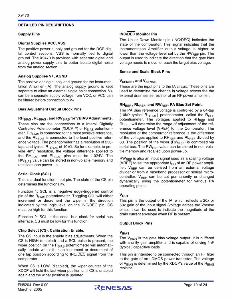
DETAILED PIN DESCRIPTIONS
Supply Pins
Digital Supplies VCC, VSS
The positive power supply and ground for the DCP digi-tal control sections. VSS is normally tied to digitalground. The X9470 is provided with separate digital andanalog power supply pins to better isolate digital noisefrom the analog section.
Analog Supplies V+, AGND
The positive analog supply and ground for the Instrumen-tation Amplifier (IA). The analog supply ground is keptseparate to allow an external single point connection. V+can be a separate supply voltage from VCC, or VCC canbe filtered before connection to V+.
Bias Adjustment Circuit Block Pins
RHBIAS , RLBIAS , and RWBIAS for VBIAS Adjustments.
These pins are the connections to a Intersil DigitallyControlled Potentiometer (XDCP™) or RBIAS potentiom-eter. RHBIAS is connected to the most positive reference,and the RLBIAS is connected to the least positive refer-ence voltage. The potentiometer has a resolution of 256-taps and typical RTOTAL of 10k. So for example, to pro-vide 4mV resolution, the voltage difference applied tothe RHBIAS and RLBIAS pins must be 1.024V. TheRWBIAS value can be stored in non-volatile memory andrecalled upon power-up.
Serial Clock (SCL).
This is a dual function input pin. The state of the CS pindetermines the functionality.
Function 1: SCL is a negative edge-triggered controlpin of the RBIAS potentiometer. Toggling SCL will eitherincrement or decrement the wiper in the directionindicated by the logic level on the INC/DEC pin. CSmust be high for this function.
Function 2: SCL is the serial bus clock for serial businterface. CS must be low for this function.
Chip Select (CS). Calibration Enable.
The CS input is the enable bias adjustments. When theCS is HIGH (enabled) and a SCL pulse is present, thewiper position on the RBIAS potentiometer will automati-cally update with either an increment or decrement ofone tap position according to INC/DEC signal from thecomparator.
When CS is LOW (disabled), the wiper counter of theXDCP will hold the last wiper position until CS is enabledagain and the wiper position is updated.
INC/DEC Monitor Pin
The Up or Down Monitor pin (INC/DEC) indicates thestate of the comparator. This signal indicates that theInstrumentation Amplifier output voltage is higher orlower than the voltage level set by the RWREF pin. Theoutput is used to indicate the direction that the gate biasvoltage needs to move to reach the target bias voltage.
Sense and Scale Block Pins
VSENSE+ and VSENSE-
These are the input pins to the IA circuit. These pins areused to determine the change in voltage across the theexternal drain sense resistor of an RF power amplifier.
RHREF , RLREF, and RWREF. PA Bias Set Point.
The PA Bias reference voltage is controlled by a 64-tap(10k typical RTOTAL) potentiometer, called the RREFpotentiometer. The voltages applied to RHREF andRLREF will determine the range of adjustment of the ref-erence voltage level (VREF) for the Comparator. Theresolution of the comparator reference is the differenceof the voltages applied to RHREF and RLREF divided by63. The position of the wiper (RWREF) is controlled viaserial bus. The RWREF value can be stored in non-vola-tile memory and recalled upon power-up.
RWREF is also an input signal used as a scaling voltage(VREF) to set the appropriate IDQ of an RF power ampli-fier. VREF can be derived from an external voltagedivider or from a baseband processor or similar micro-controller. VREF can be set permanently or changeddynamically using the potentiometer for various PAoperating points.
VOUT
This pin is the output of the IA, which reflects a 20x or50x gain of the input signal (voltage across the Vsensepins). It can be used to indicate the magnitude of thedrain current envelope when RF is present.
Output Block Pins
VBIAS
The VBIAS is the gate bias voltage output. It is bufferedwith a unity gain amplifier and is capable of driving 1nF(typical) capacitive loads.
This pin is intended to be connected through an RF filterto the gate of an LDMOS power transistor. The voltageof VBIAS is determined by the XDCP’s value of the RBIASresistor.
FN8204 Rev 0.00 Page 10 of 24March 8, 2005

X9470
Other Pins
SHDN
SHDN is an input pin that is used to shutdown the VBIASoutput voltage follower. When the SHDN pin is HIGH,the VBIAS pin is pulled to VSS. When the device is shut-down, the current RBIAS wiper position will be main-tained in the wiper counter register. When shutdown isdisabled, the wiper returns to the same wiper positionbefore shutdown was invoked. Note that when thedevice is taken out of shutdown mode (SHDN goes fromHIGH to LOW), the CS input must be cycled once toenable calibration.
SDA
Serial bus data input/output. Bi-directional. External pul-lup is required.
A0, A1, A2
Serial bus slave address pins. These pins are used todefined a hardware slave address. This will allow up to 8of the X9470’s to be shared on one two-wire bus. Theseare useful if several X9470’s are used to control the biasvoltages of several LDMOS Power Transistors in a sin-gle application. Default hardware slave address is “000”if left unconnected due to internal pull-down resistor.
TYPICAL APPLICATION
The X9470 can be used along with a microprocessor andtransmit control chips to control and coordinate FET bias-ing (see Figure 1). The CS, SCL, and SDA signals arerequired to control the X9470 Bias Adjustment CircuitBlock. An internal RWREF voltage is provided via a pro-grammable voltage divider between the RHREF andRLREF pins and is used to set the voltage reference of thecomparator. The shutdown (SHDN) and bias voltage indi-cators (INC/DEC) are additional functions that offer FETcontrol, monitoring, and protection.
Typically, the closed loop setup of the X9470 allows forfinal calibration of a power amplifier at production test.The CS and SCL pins are used to perform this calibrationfunction. Once in a base station, the amplifier can then bere-calibrated any time that there is no RF signal present.The bias setting block can also be used open loop toadjust gate bias or can be shutdown using the SHDN pin.The sense and scale block can be used for amplifierpower monitoring diagnostics as well.
The range of the drain bias current operating point of theLDMOS FET is set by an external reference across thereference potentiometer. The wiper of the potentiometersets the trip point for comparison with VP , the amplifiedvoltage across RSENSE, the drain resistor. The output ofthe comparator causes the RBIAS potentiometer to incre-ment or decrement automatically on the next SCL clockcycle. This RBIAS potentiometer is configured as a volt-age divider with a buffered wiper output which drives thegate voltage of an external LDMOS FET.
Once the optimum bias point is reached, the RBIAS valueis latched into a wiper counter register. Again, the VBIASgate voltage can be updated continuously or periodicallydepending on the system requirements.
Both terminals of the RBIAS potentiometer are access-ibleand can be driven by external reference voltages toachieve a desired IDQ vs. gate voltage resolution, as wellas supporting temperature compensation circuitry.
In summary, the X9470 provides full flexibility on settingthe operating bias point and range of an external RFpower amplifier for GSM, EDGE, UMTS, CDMA or othersimilar applications.
FN8204 Rev 0.00 Page 11 of 24March 8, 2005
X9470
Figure 1. Typical Application
X9470 FUNCTIONAL DESCRIPTION
This section provides detail description of the following:
– Sense and Scale Block Description
– Bias Adjustment Control Block Description
– Output Block Description
– Bias Adjustment and Storage Description
SENSE AND SCALE BLOCK
The Sense and Scale Circuit Block (Figure 2) implementsan instrumentation amplifier whose inputs (VSENSE+ andVSENSE-) are across an external sense resistor in the draincircuit of an RF Power FET. VSENSE+ is connected to VDD,the drain voltage source for the RF power FET, andVSENSE- pin is connected to the other end the externalsense resistor.
An internal instrumentation amplifier (IA) will sense theV and amplify it by a gain factor of K1 (see Equation 1).The resulting output is compared with VREF at the com-parator. VREF can be a fixed reference voltage oradjusted by using the 64-tap digital potentiometer. Theoutput of the comparator is used to increment or decre-ment the RBIAS potentiometer in the Bias AdjustmentCircuit Block. The gain factor K1 is designed such thatthe Sense and Scale Block will set the Bias AdjustmentCircuit Block to operate in a given voltage range (mV)vs. drain current adjustment (mA).
The output of the IA is also available at the pin Vout toenable drain current monitoring. The gain at Vout is fixedat a factor of K2, lower than K1 so that high IDQ currentswill not cause saturation of the Vout signal. The equationfor Vout is given as:
BIAS ADJUSTMENT CIRCUIT BLOCK
There are three sections of this block (Figure 3): theinput control, counter and decode section (1), the resis-tor array (2); and the non-volatile register (3). The inputcontrol section operates just like an up/down counter.The input of the counter is driven from the output of thecomparator in the Sense and Scale Block and is clockedby the SCL signal. The output of this counter is decodedto select one of the taps of a 256-tap digital potentiome-ter.
A0
A2
VCC VSS
V+AGND
Comparator
choke
RF PA in
RSENSE
VDD
VREF
VSENSE+
VBIAS
INC/DEC
InstrumentationAmplifier
V
CS
VOUT
VSENSE–
RREF
RWREF RLREF
SHDN
+
–
EEPROM
SCL
SDA
A1
Vbiascontrol
VREFcontrol
I2Cinterface
Control & Status Registers
RFout
RHREF
RBIAS
VP
RHBIAS RLBIASRWBIAS
FILTER
VB
IAS
(Unbuffered)
RF ImpedanceMatching
CBULK
Class A Example
IDQ VREF
K1 * RSENSE
K1 is fixed 50x for the internal comparator input.
(1)
V = IDQ * RSENSE
VOUT = K2 * V
K2 is fixed to 20x for the Vout pin
FN8204 Rev 0.00 Page 12 of 24March 8, 2005

X9470
Figure 2. Sense and Scale Block Diagram
The wiper of the digital potentiometer acts like itsmechanical equivalent and does not move beyond thelast position. That is, the counter does not wrap aroundwhen clocked to either extreme. The electronic switchesin the potentiometer operate in a “make before break”mode when the wiper changes tap positions. If the wiperis moved several positions, multiple taps are connectedto the wiper for tIW (SCL to RWBIAS change).
When the device is powered-up, the X9470 will load thelast saved value from the non-volatile memory into theWCR. Note that the current wiper position can be savedinto non-volatile memory register by using the SCL andCS pins as shown in Figure 4.
Important note: the factory setting of the wiper counterregister is the ZERO-position (0 of 255 taps). This is thedefault wiper position.
Bias Adjustment Block Instructions and Program-ming. The SCL, INC/DEC (internal signal) and CSinputs control the movement of the wiper along the resis-tor array. (See Table 1) With CS set HIGH, the device isselected and enabled to respond to the INC/DEC andSCL inputs. HIGH to LOW transitions on SCL will incre-ment or decrement RBIAS (depending on the state of theINC/DEC input). The INC/DEC input is derived from theoutput of the comparator of the Sense and Scale Block.
Storing Bias Resistor Values in Memory. Wiper val-ues are stored to VOLATILE memory automaticallywhen CS is HIGH and INC/DEC either transitions fromHIGH to LOW or from LOW to HIGH. Wiper values arestored to NON-VOLATILE memory during Byte Write oras described in the following section.
Table 1. Mode Selection
* When coming out of shutdown, the CS pin must be cycled once before biasadjustment is enabled.
INC/DEC RWREF RLREFRHREF VOUT
VDDVSENSE+
RSENSE VSENSE–
10k64-tap
VREF
ComparatorINC/DEC
~1k
PrecisionI-Amp
Cint~2pF ±10%
}
V
IDQ
RFPAOutchoke
Vgate
RF PA in
K2 = 20X
K1 = 50X
SDA CS* SCLINC / DEC Mode
H H H VBIAS is incremented one tap position.
H H L VBIAS is decremented one tap position.
H H X Lock Wiper Position. Save to volatile memory. (BiasLock™)
X L X X Open Loop.
or
FN8204 Rev 0.00 Page 13 of 24March 8, 2005

X9470
Figure 3. Bias Adjustment Block Diagram
NON-VOLATILE STORE OF THE BIAS POSITION
The following procedure will store the values for the Rrefand Rbias wiper positions in Non-Volatile memory. Thissequence is intended to be performed after a BiasLockcalibration sequence to simplify storage. If BiasLock hasnot been achieved, then the Rbias wiper position maychange when the CS pin is brought high and SCL beginsclocking. See Figure 4 for the actual sequence.
1. Set the WEL bit with a write command (02h to regis-ter 0Fh)
2. Peform a calibration and achieve BiasLock. LeaveCS pin high.
3. Write the address byte only (START, followed bydevice/slave address and a 0 for a write, see page19).
4. Perform a STOP command.5. With SCL still low, bring the CS low. The falling edge
of the CS will initiate the NV write.
The WEL bit may be reset afterwards to prevent furtherNV writes.
INC/DEC FUNCTION
The INC/DEC pin is an open-drain logic output thattracks the activity of the increment/decrement compara-tor. A logic HIGH at INC/DEC indicates that the IDQ didnot rise up to the desired setting indicated by VREF whilea logic LOW at the INC/DEC pin indicates that the IDQ ishigher than the desired setting.
INC/DEC is used as an internal control signal as well. Asan example, when INC/DEC is LOW, the Bias Adjust-ment Circuit Block will start to move the Rbias resistorwiper towards the RLBIAS terminal end when CS is HIGHand SCL is clocking. Consequently, the VBIAS voltagewill decrease, and the IDQ decreases to meet the desiredVREF setting.
The INC/DEC signal can also be used to detect a dam-aged RF power FET. For instance, If INC/DEC staysHIGH during and after a calibration sequence it mayindicate that the RF power FET has failed. This indicatorcan also be used with a level sense on the VOUT pin toperform diagnostics.
SHUTDOWN MECHANISM
This hardware control shutdown pin (SHDN) will pull thevoltage of VBIAS to VSS with an internal pull down resis-tor. When shutdown is disabled (VBIAS is active whenSHDN is LOW), the VBIAS voltage will move to the previ-ous desired bias voltage.
It will take less than a microsecond to enable the internaloutput buffer depending on the loading condition at theVBIAS pin.
OUTPUT (VBIAS)
VBIAS is a buffered output of RWBIAS (wiper output). Itcan deliver a high current for driving up to typically 1nFcapacitive loading with stable performance and fast set-tling time.
Gate BiasOp Amp
+
–
RWBIAS
RHBIAS
RLBIAS
Legend
External pin/signal
Internal node/signal
SCL
CS
2
3
1
VBIAS (unbuffered)
VBIAS
SHDN
to LDMOS gate
10k256-tap
RBIAS
INCU/DCS
INC/DEC
XDCPMemory and Control
WCR (Rbias)
Bias Registernon-volatile
Power-On Recall(POR)
Note:1) WCR = Wiper Control Register
INC/DEC is logic HIGH or LOWfrom Sense/Scale Blockand is used to increment or decrement the Rbias resistor(XDCP) to adjust the gate voltage.
FN8204 Rev 0.00 Page 14 of 24March 8, 2005

X9470
A single pole filter should be placed in between theVBIAS output and the RF input signal to isolate any highfrequency noise.
Figure 4. Non-Volatile Store of the Bias Position
X9470 PRINCIPLES OF OPERATION
The X9470 is a Bias Controller that contains all the nec-essary analog components for closed-loop DC bias con-trol of LDMOS Transistors in RF Applications. TheX9470 provides a mechanism to periodically set DC biasoperating points of Class A or AB-type amplifiers toaccount for VGS drift and temperature variations. The fol-lowing is an example of X9470 operation.
The X9470 incorporates an instrumentation amplifier,comparator and buffer amplifier along with resistor arraysand their associated registers and counters. The serialinterface provides direct communication between the hostand the X9470. This section provides a detailed exampleof how the X9470 can be used to calibrate and dynami-cally set the optimum bias operating point of an RF poweramplifier (see Figure 5):
– State 0: Power-on Monitor Mode
– State 1: DC-bias Setting When No RF is Present [Cali-bration]
– State 2: Calibration Disable When RF is Present
– State 3: PA Standby Mode. Dynamic Adjustment for VGS drift and Temperature variation
– State 4: Power Off (Shutdown) Mode [Turn off the Power Amplifier]
State 0: Monitor Mode
The VOUT and INC/DEC outputs of the X9470 can be used for monitoring and diagnostic purposes. Since VOUT has a lower gain (20x, default) than the internal IA output, it can handle higher drain sense current while keeping the output below the rail. This allows normal PA power monitoring, and over-current sensing using an external comparator. The INC/DEC pin can be monitored during calibration to see if there is no change, which indicates LDMOS functional problems. Note that the INC/DEC sta-tus is also available in the status register for software sta-tus reads.
State 1: DC-bias Setting When No RF is Present [Cal-ibration]
At calibration, the DC bias operating point of the LDMOSPower Amplifier must be set. As soon as the BiasAdjustment Circuit Block is enabled (CS enabled, SDAhigh, and SCL pulse provided), the X9470 will automati-cally calibrate the external Power Amplifier by continu-ally sampling the drain current of the external PowerAmplifier and make adjustments to the gate voltage ofthe amplifier (See Figure 6).
Initiateshigh voltage writecycle
tWR
Stored inNon-volatilememory
CS
SCL
SDA
Non-volatile Write of RBIAS and RREF value Using SDA, SCL and CS pins
RBIAS non-volatile register
Set WELbit
Calibrationand Bias Lock
SetAddress Byte
Stop
1 2 3 4
5
FN8204 Rev 0.00 Page 15 of 24March 8, 2005

X9470
Figure 5. Operating modes X9470
When no RF signal is present, the instrumentationamplifier of the X9470 senses the drain current as a volt-age drop, V, across an external drain Rsense resistor.The V is amplified and compared to an external scalingvoltage, VREF . Any difference between V and VREFresults in a resistive increment or decrement of the inter-nal RBIAS potentiometer.
The RBIAS potentiometer is used as a voltage dividerwith the RHBIAS and RLBIAS terminals setting the upperand lower voltage limits of the unbuffered RWBIAS volt-age. The resolution of the RBIAS potentiometer resistor is0.4% of the difference of voltage across the RHBIAS andRLBIAS terminals. The RTOTAL is typically 10kwith 256-taps. So, for example, if the difference between theRHBIAS and RLBIAS terminals is 1.024V, then the stepaccuracy is 4mV.
The voltage at the RWBIAS pin is then fed into the VBIASvoltage follower. The VBIAS pin is a buffered output that isused to drive the gate of an LDMOS transistor.
The scaling voltage, VREF, set by the RREF potentiome-ter, sets the calibrated operating point of the LDMOSAmplifier.
On edge transitions of the INC/DEC signal, the X9470 willlatch the current wiper position - this is known as “BiasLock™” mode. This is shown in Figure 6. When BiasLockoccurs, the comparator hysteresis will allow INC/DEC tochange state only after the IA output changes by more than20mV. This will prevent toggling of the VBIAS output unlessthe drain bias current is constantly changing.
State 2: DC-bias Disable When RF is Present (optional)
When an RF signal is present, the X9470 is put intostandby mode (open loop). The X9470 is in standbymode when the CS pin is disabled so that the RBIASpotentiometer holds the last wiper position. The pres-ence of an RF signal at the input of a Class A or ABamplifier increases the current across the Rsense resis-tor. Over a period of time, the temperature of theLDMOS also increases and the LDMOS also experi-ences VGS drift. Therefore the DC biasing point that wasset during State 1 (calibration) is not optimal. Adjust-ments to the gate voltage will need to be made to opti-mize the operation of the LDMOS PA. This is done inState 3.
Choose Vref to scale IDQ, perform calibration,State 1
State 2
State 3
State 4
PATransmit Mode
PACalibration Mode
PAStandby Mode
PAOff Mode
Disable Bias Adjustment,
Recalibrate bias point for drift and temperature.
Rbias resistor will automatically increment or decrement for optimal operating point continuously
Turn off PA
Latch bias point for DC bias current in wiper counter
PA Enabled, Vout and INC/DEC Monitored for statusState 0PA
Monitor Mode
FN8204 Rev 0.00 Page 16 of 24March 8, 2005

X9470
State 3: PA Standby Mode, DC Bias Adjustment [Compensation for VGS Drift and Temperature Variation]
When the Power Amplifier is in Standby Mode theX9470 allows for dynamic adjustment of the DC biasingpoint to take into account both VGS drift and temperaturevariation. Dynamic biasing is achieved with the X9470by using the CS, and SCL pins. For example, the SCLpin can be a steady clock and the CS pin can be used asa control signal to enable/disable the Bias AdjustmentBlock.
Figure 6 illustrates how the X9470 can be used fordynamic biasing. Upon the presence of an RF signal, theCS pin is pulled LOW. This will prevent the X9470 fromchanging the VBIAS voltage during IDQ peak currents.Once the RF signal is no longer present, the CS pin canbe enabled (closed loop), SDA high and the X9470 BiasAdjustment Circuit moves the VBIAS voltage (the gatevoltage of the FET) to meet the average IDQ bias pointfor optimum amplifier performance.
State 4: Power Off Mode
During power saving or power-off modes the X9470 canbe shut down via the SHDN pin. This pin pulls the outputof the VBIAS pin LOW.
Figure 6. Dynamic Biasing Technique: Automatic DC Bias Operating Point Adjustment
State 0MonitorMode
State 1Calibration
(no RF present)
State 2RF present
State 3Recalibrate bias
point for driftand temperature
State 4shutdown
Set Operating Range Scale for Bias Adjustment
RF signal
VREF
CS
SCL
INC/DEC
SHDN
VBIAS
1
2
3 45
6
Rbias default iszero point of Rtotal
Latch Rbias DC pointin calibration vs VREF
RF presentTurn offBiasAdjustment
Rbias increase/decreaseafter RF present due totemperature increase &VGS-threshold drift
IDQ vs. gatevoltage biasoptimized
Shutdown
BiasLockSaves wiper position to volatile memory
Bias Adjustment ON
Bias Adjustment OFF
Bias Adjustment ON
Automatic Bias Adjustment
BiasLock
FN8204 Rev 0.00 Page 17 of 24March 8, 2005
X9470
X9470 STATUS REGISTER (SR) AND CONTROL REGISTER (CR) INFORMATION
Table 2. Status Register (SR)
STATUS REGISTER (SR)
The Status Register is located at address 0F<hex>. Thisis a register used to control the write enable latches, andmonitor status of the SHDN, INC/DEC, and CS pin. Thisregister is separate from the Control Register.
SR7: SHDN: Vbias SHDN Flag. Read Only—Volatile.The bit keeps status of the shutdown pin, SHDN. Whenthis bit is HIGH, the SHDN pin is active and the VBIASoutput is disabled. When this bit is LOW, the SHDN pinis low and VBIAS output is enabled.
SR6: INC/DEC : Read Only—Volatile. This bit keepsstatus of the INC/DEC pin. When this bit is HIGH thecounter is in increment mode, when this bit is LOW thecounter is in decrement mode.
SR4: CS: Read Only—Volatile. This bit keeps status onthe CS pin. When this bit is HIGH, the X9470 is in closedloop mode (Rbias adjustment enabled). When this bit isLOW the x9470 is in open loop mode (no Rbias adjust-ments).
SR2, SR3, SR5: Read only
For internal test usage, should be set to 0 during SRwrites.
SR1: WEL: Write Enable Latch—Volatile
The WEL bit controls the access to the registers during awrite operation. This bit is a volatile latch that powers upin the LOW (disabled) state. While the WEL bit is setLOW, Nonvolatile writes to the registers will be ignored,and all writes to registers will be volatile. The WEL bit isset by writing a “1” to the WEL bit and zeroes to theother bits of the Status Register. Once this write opera-tion is completed and a STOP command is issued, non-volatile writes will then occur for all NOVRAM registersand control bits. Once set, the, WEL bit remains set untileither reset to 0 (by writing a “0” to the WEL bit andzeroes to the other bits of the Status Register) or untilthe part powers up again.
SR0: Gain - NOVRAM
Selects VOUT and IA gain. When SR0=0, VOUTgain = 20x, IA gain = 50x. When SR0 = 1, VOUTgain = 50x, and IA gain = 20x. Default setting is 0.
CONTROL REGISTERS (CR)
The control registers are organized for byte operations.Each byte has a unique byte address as shown in Table3 below.
Table 3. Control Registers (CR)
Note: 02H to 0EH are reserved for internal manufacturing use.
Byte
Addr SR7 SR6 SR5 SR4 SR3 SR2 SR1 SR0
0F hex SHDN INC/DEC 0 CS 0 0 WEL Gain
Byte
Addr.
<HEX> DescriptionReg
Name
Bit
Memory Type 7 6 5 4 3 2 1 0
00 hex DCP for Vbias Vbias Vb7 Vb6 Vb5 Vb4 Vb3 Vb2 Vb1 Vb0 NOVRAM
01 hex DCP for VREF Vref X X Vr5 Vr4 Vr3 Vr2 Vr1 Vr0 NOVRAM
FN8204 Rev 0.00 Page 18 of 24March 8, 2005

X9470
X9470 BUS INTERFACE INFORMATION
Figure 7. Slave Address, Word Address, and Data Bytes - Write Mode
Figure 8. Slave Address, Word Address, and Data Bytes - Read Mode
Slave Address, Byte Address, and Data Byte
The byte communication format for the serial bus isshown in Figures 7 and 8 above. The first byte, BYTE 0,defines the device indentifier, 0101 in the upper half; andthe device slave address in the low half of the byte. Theslave address is determined by the logic values of theA0, A1, and A2 pins of the X9470. This allows for up to 8unique addresses for the X9470. The next byte, BYTE 1,is the Byte Address. The Byte Address identifies aunique address for the Status or Control Registers asshown in Table 3. The following byte, Byte 2, is the databyte that is used for READ and WRITE operations.
Start Condition
All commands are preceded by the start condition, whichis a HIGH to LOW transition of SDA when SCL is HIGH.The device continuously monitors the SDA and SCLlines for the start condition and will not respond to anycommand until this condition has been met. See Figure 9.
Slave Address Byte
Byte 0
D7 D6 D5 D2D4 D3 D1 D0
A0A7 A2A4 A3 A1
Data Byte
Byte 2
A6 A5
0 1 0 S11 S0 R/W=0S2
Device Identifier
Byte Address
Byte 1
Slave Address
0Fh : SR
00h : VBIAS
01h : VREF
Slave Address Byte
Byte 0
D7 D6 D5 D2D4 D3 D1 D0
D0D7 D2D4 D3 D1
Data Byte
Byte 2
D6 D5
0 1 0 S11 S0 R/WS2
Device Identifier
Data Byte
Byte 1
Slave Address
FN8204 Rev 0.00 Page 19 of 24March 8, 2005

X9470
Stop Condition
All communications must be terminated by a stop condi-tion, which is a LOW to HIGH transition of SDA whenSCL is HIGH. The stop condition is also used to placethe device into the Standby power mode after a readsequence. A stop condition can only be issued after thetransmitting device has released the bus. See Figure 9.
Acknowledge
Acknowledge is a software convention used to indicatesuccessful data transfer. The transmitting device, eithermaster or slave, will release the bus after transmittingeight bits. During the ninth clock cycle, the receiver willpull the SDA line LOW to acknowledge that it receivedthe eight bits of data. Refer to Figure 10.
The device will respond with an acknowledge after rec-ognition of a start condition and if the correct DeviceIdentifier and Select bits are contained in the SlaveAddress Byte. If a write operation is selected, the devicewill respond with an acknowledge after the receipt ofeach subsequent eight bit word. The device willacknowledge all incoming data and address bytes,except for:
– The Slave Address Byte when the Device Identifier and/or Select bits are incorrect
– The 2nd Data Byte of a Status Register Write Opera-tion (only 1 data byte is allowed)
Figure 9. Valid Start and Stop Conditions
Figure 10. Acknowledge Response From Receiver
Figure 11. Valid Data Changes on the SDA Bus
SCL
SDA
Start Stop
SCL fromMaster
Data Outputfrom Transmitter
Data Outputfrom Receiver
81 9
Start Acknowledge
SCL
SDA
Data Stable Data Change Data Stable
FN8204 Rev 0.00 Page 20 of 24March 8, 2005

X9470
WRITE OPERATIONS
Byte Write
For a write operation, the device requires the SlaveAddress Byte and the Word Address Bytes. This givesthe master access to any one of the words in the array.Upon receipt of each address byte, the X9470 respondswith an acknowledge. After receiving the address bytesthe X9470 awaits the eight bits of data. After receivingthe 8 data bits, the X9470 again responds with anacknowledge. The master then terminates the transferby generating a stop condition. The X9470 then beginsan internal write cycle of the data to the nonvolatilememory. During the internal write cycle, the deviceinputs are disabled, so the device will not respond to anyrequests from the master. The SDA output is at highimpedance. See Figure 12.
A write to a protected block of memory is ignored, butwill still receive an acknowledge. At the end of the writecommand, the X9470 will not initiate an internal writecycle, and will continue to ACK commands.
Stops and Write Modes
Stop conditions that terminate write operations must besent by the master after sending at least 1 full data byteand it’s associated ACK signal. If a stop is issued in themiddle of a data byte, or before 1 full data byte + ACK issent, then the X9470 resets itself without performing thewrite. The contents of the array are not affected.
Acknowledge Polling
Disabling of the inputs during nonvolatile write cyclescan be used to take advantage of the typical 5ms writecycle time. Once the stop condition is issued to indicatethe end of the master’s byte load operation, the X9470initiates the internal nonvolatile write cycle. Acknowl-edge polling can begin immediately. To do this, the mas-ter issues a start condition followed by the SlaveAddress Byte for a write or read operation. If the X9470is still busy with the nonvolatile write cycle then no ACKwill be returned. When the X9470 has completed thewrite operation, an ACK is returned and the host canproceed with the read or write operation. Refer to theflow chart in Figure 15.
READ OPERATIONS
There are three basic read operations: Current AddressRead, Random Read, and Sequential Read.
Current Address Read
Internally the X9470 contains an address counter thatmaintains the address of the last word read incrementedby one. Therefore, if the last read was to address n, thenext read operation would access data from addressn+1. On power-up, the address is initialized to 0h. In thisway, a current address read immediately after thepower-on reset can download the entire contents ofmemory starting at the first location. Upon receipt of theSlave Address Byte with the R/W bit set to one, theX9470 issues an acknowledge, then transmits eight databits. The master terminates the read operation by notresponding with an acknowledge during the ninth clockand issuing a stop condition. Refer to Figure 13 for theaddress, acknowledge, and data transfer sequence.
FN8204 Rev 0.00 Page 21 of 24March 8, 2005

X9470
Figure 12. Byte Write Sequence
Figure 13. Current Address Read Sequence
Figure 14. Random Address Read Sequence
Start
Stop
Data
ACK
ACK
SDA Bus
Signals FromThe Slave
Signals fromthe Master
0
ACK
Byte Address 0
A0A1A20 101
Slave Address
Device ID
Start
Stop
Data
ACK
SDA Bus
Signals fromthe Slave
Signals from theMaster
Slave Address
1A0A1A20 101
Device ID
ACK
ACK
Start
Stop
Data
Start
SDA Bus
Signals fromthe Slave
Signals from theMaster
Byte Address 0
ACK
Slave Address
0A0A1A20 101
Device ID
ACK
Slave Address
1A0A1A20 101
Device ID
ACK
FN8204 Rev 0.00 Page 22 of 24March 8, 2005

X9470
Figure 15. Acknowledge Polling Sequence
It should be noted that the ninth clock cycle of the readoperation is not a “don’t care.” To terminate a read oper-ation, the master must either issue a stop conditionduring the ninth cycle or hold SDA HIGH during the ninthclock cycle and then issue a stop condition.
Random Read
Random read operations allows the master to accessany location in the X9470. Prior to issuing the SlaveAddress Byte with the R/W bit set to zero, the mastermust first perform a “dummy” write operation.
The master issues the start condition and the slaveaddress byte, receives an acknowledge, then issues theword address bytes. After acknowledging receipt of eachword address byte, the master immediately issuesanother start condition and the slave address byte withthe R/W bit set to one. This is followed by an acknowl-edge from the device and then by the eight bit dataword. The master terminates the read operation by notresponding with an acknowledge and then issuing a stopcondition. Refer to Figure 13 for the address, acknowl-edge, and data transfer sequence.
In a similar operation called “Set Current Address,” thedevice sets the address if a stop is issued instead of thesecond start shown in Figure 14. The X9470 then goesinto standby mode after the stop and all bus activity willbe ignored until a start is detected. This operation loadsthe new address into the address counter. The next Cur-rent Address Read operation will read from the newlyloaded address. This operation could be useful if themaster knows the next address it needs to read, but isnot ready for the data.
ACK returned?
Issue Slave Address Byte
(Read or Write)
Byte load completed by issuing STOP.Enter ACK Polling
Issue STOP
Issue START
NO
YES
Issue STOPNO
Continue normal Read or Write
command sequence
PROCEED
YES
nonvolatile write Cycle complete.
Continue command sequence?
FN8204 Rev 0.00 Page 23 of 24March 8, 2005
X9470
Intersil products are manufactured, assembled and tested utilizing ISO9001 quality systems as notedin the quality certifications found at www.intersil.com/en/support/qualandreliability.html
Intersil products are sold by description only. Intersil may modify the circuit design and/or specifications of products at any time without notice, provided that such modification does not, in Intersil's sole judgment, affect the form, fit or function of the product. Accordingly, the reader is cautioned to verify that datasheets are current before placing orders. Information furnished by Intersil is believed to be accurate and reliable. However, no responsibility is assumed by Intersil or its subsidiaries for its use; nor for any infringements of patents or other rights of third parties which may result from its use. No license is granted by implication or otherwise under any patent or patent rights of Intersil or its subsidiaries.
For information regarding Intersil Corporation and its products, see www.intersil.com
For additional products, see www.intersil.com/en/products.html
© Copyright Intersil Americas LLC 2005. All Rights Reserved.All trademarks and registered trademarks are the property of their respective owners.
PACKAGING INFORMATION
NOTE: ALL DIMENSIONS IN INCHES (IN PARENTHESES IN MILLIMETERS)
24-Lead Plastic, TSSOP Package Type V
.169 (4.3)
.177 (4.5).252 (6.4) BSC
.026 (.65) BSC
.303 (7.70)
.311 (7.90)
.002 (.06)
.005 (.15)
.047 (1.20)
.0075 (.19)
.0118 (.30)
See Detail “A”
.031 (.80).041 (1.05)
0 - 8
.010 (.25)
.020 (.50)
.030 (.75)
Gage Plane
Seating Plane
Detail A (20X)
FN8204 Rev 0.00 Page 24 of 24March 8, 2005