Embed Size (px)
Citation preview

8/6/2019 Datasheet p89c51
http://slidepdf.com/reader/full/datasheet-p89c51 1/68
PhilipsSemiconductors
P89C51RA2xx/RB2xx/RC2xx/RD2xx80C51 8-bit Flash microcontroller family8KB/16KB/32KB/64KB ISP/IAP Flash with512B/512B/512B/1KB RAM
Preliminary dataSupersedes data of 2002 May 20 2002 Jul 18
INTEGRATED CIRCUITS

8/6/2019 Datasheet p89c51
http://slidepdf.com/reader/full/datasheet-p89c51 2/68
Philips Semiconductors Preliminary data
P89C51RA2/RB2/RC2/RD2xx80C51 8-bit Flash microcontroller family8KB/16KB/32KB/64KB ISP/IAP Flash with 512B/512B/512B/1KB RAM
22002 Jul 18
DESCRIPTIONThe P89C51RA2/RB2/RC2/RD2xx contains a non-volatile
8KB/16KB/32KB/64KB Flash program memory that is both parallel
programmable and serial In-System and In-Application
Programmable. In-System Programming (ISP) allows the user todownload new code while the microcontroller sits in the application.
In-Application Programming (IAP) means that the microcontroller
fetches new program code and reprograms itself while in the
system. This allows for remote programming over a modem link.
A default serial loader (boot loader) program in ROM allows serial
In-System programming of the Flash memory via the UART without
the need for a loader in the Flash code. For In-Application
Programming, the user program erases and reprograms the Flash
memory by use of standard routines contained in ROM.
The device supports 6-clock/12-clock mode selection by
programming a Flash bit using parallel programming or
In-System Programming. In addition, an SFR bit (X2) in the clock
control register (CKCON) also selects between 6-clock/12-clock
mode.
Additionally, when in 6-clock mode, peripherals may use either 6
clocks per machine cycle or 12 clocks per machine cycle. This
choice is available individually for each peripheral and is selected by
bits in the CKCON register.
This device is a Single-Chip 8-Bit Microcontroller manufactured in an
advanced CMOS process and is a derivative of the 80C51
microcontroller family. The instruction set is 100% compatible with
the 80C51 instruction set.
The device also has four 8-bit I/O ports, three 16-bit timer/event
counters, a multi-source, four-priority-level, nested interrupt structure,
an enhanced UART and on-chip oscillator and timing circuits.
The added features of the P89C51RA2/RB2/RC2/RD2xx make it a
powerful microcontroller for applications that require pulse width
modulation, high-speed I/O and up/down counting capabilities suchas motor control.
FEATURES
• 80C51 Central Processing Unit
• On-chip Flash Program Memory with In-System Programming
(ISP) and In-Application Programming (IAP) capability
• Boot ROM contains low level Flash programming routines for
downloading via the UART
• Can be programmed by the end-user application (IAP)
• Parallel programming with 87C51 compatible hardware interface
to programmer
• Supports 6-clock/12-clock mode via parallel programmer (default
clock mode after ChipErase is 12-clock)
• 6-clock/12-clock mode Flash bit erasable and programmable via
ISP
• 6-clock/12-clock mode programmable “on-the-fly” by SFR bit
• Peripherals (PCA, timers, UART) may use either 6-clock or
12-clock mode while the CPU is in 6-clock mode
• Speed up to 20 MHz with 6-clock cycles per machine cycle
(40 MHz equivalent performance); up to 33 MHz with 12 clocks
per machine cycle
• Fully static operation
• RAM expandable externally to 64 kbytes
• Four interrupt priority levels
• Seven interrupt sources
• Four 8-bit I/O ports
• Full-duplex enhanced UART
– Framing error detection
– Automatic address recognition
• Power control modes
– Clock can be stopped and resumed
– Idle mode
– Power down mode
• Programmable clock-out pin
• Second DPTR register
• Asynchronous port reset
• Low EMI (inhibit ALE)
• Programmable Counter Array (PCA)
– PWM
– Capture/compare

8/6/2019 Datasheet p89c51
http://slidepdf.com/reader/full/datasheet-p89c51 3/68
Philips Semiconductors Preliminary data
P89C51RA2/RB2/RC2/RD2xx80C51 8-bit Flash microcontroller family8KB/16KB/32KB/64KB ISP/IAP Flash with 512B/512B/512B/1KB RAM
2002 Jul 18 3
SELECTION TABLE
Type Memory TimersSerial
Interfaces
R A M
R O M
O T P
F l a s h
# o f T i m e r s
P W M
P C A
W D
U A R T
I 2 C
C A N
S P I
A D C b i t s / c h .
I / O P i n s
I n t e r r u p t s
( E x t . ) / L e v e l s
P r o g r a m
S e c u r i t y
D e f a u l t C l o c k
R a t e 1
O p t i o n a l
C l o c k R a t e 1
R e s e t a c t i v e
l o w / h i g h ?
Max.Freq.at 6-clk / 12-clk(MHz)
Freq.Rangeat 3V(MHz)
Freq.Rangeat 5V(MHz)
P89C51RD2xx 1K – – 64K 4 √ √ √ √ – – – – 32 7(2)/4 √ 12-clk 6-clk H 20/33 – 0-20/33
P89C51RC2xx 512B – – 32K 4 √ √ √ √ – – – – 32 7(2)/4 √ 12-clk 6-clk H 20/33 – 0-20/33
P89C51RB2xx 512B – – 16K 4 √ √ √ √ – – – – 32 7(2)/4 √ 12-clk 6-clk H 20/33 – 0-20/33
P89C51RA2xx 512B – – 8K 4 √ √ √ √ – – – – 32 7(2)/4 √ 12-clk 6-clk H 20/33 – 0-20/33
NOTE:1. P89C51Rx2Hxx devices have a 6-clk default clock rate (12-clk optional). Please also see Device Comparison Table.
DEVICE COMPARISON TABLE
Item 1st generation of Rx2 devices 2nd generation of Rx2 devices
(this data sheet)
Difference
Type description P89C51Rx2Hxx(x) P89C51Rx2xx(x) No more letter ‘H’
Programming algo-rithm
When using a parallel programmer,be sure to selectP89C51Rx2Hxx(x) devices
When using a parallel programmer, besure to select P89C51Rx2xx(x) de-vices (no more letter ‘H’)
Different programming algorithmdue to process change
Clock mode (I) 6-clk default, OTP configuration bitto program to 12-clk mode usingparallel programmer (cannot beprogrammed back to 6-clk)
12-clk default, Flash configuration bitto program to 6-clk mode using paral-lel programmer or ISP (can be repro-grammed)
More flexibility for the end user,more compatibility to olderP89C51Rx+ parts
Clock mode (II) N/A 6-clock/12-clock mode programmable“on the fly” by SFR bit X2 (CKCON.0)
Clock mode can be changed bysoftware
Peripheral clockmodes
N/A Peripherals can be run in 12-clk modewhile CPU runs in 6-clk mode
More flexibility, lower power con-sumption
Flash block structure Two 8-Kbyte blocks1–3 16-Kbyte blocks
2–16 4-Kbyte blocks More flexibility
ORDERING INFORMATION
MEMORY TEMPERATURE FREQUENCY (MHz)
NUMBER1 FLASH RAM RANGE (°C)AND PACKAGE
RANGE 6-CLOCKMODE
12-CLOCKMODE
DWG #
1. P89C51RA2BA/01 8 KB 512 B 0 to +70, PLCC 4.5–5.5 V 0 to 20 MHz 0 to 33 MHz SOT187-2
2. P89C51RA2BBD/01 8 KB 512 B 0 to +70, LQFP 4.5–5.5 V 0 to 20 MHz 0 to 33 MHz SOT389-1
3. P89C51RB2BA/01 16 KB 512 B 0 to +70, PLCC 4.5–5.5 V 0 to 20 MHz 0 to 33 MHz SOT187-2
4. P89C51RB2BBD/01 16 KB 512 B 0 to +70, LQFP 4.5–5.5 V 0 to 20 MHz 0 to 33 MHz SOT389-1
5. P89C51RC2BN/01 32 KB 512 B 0 to +70, PDIP 4.5–5.5 V 0 to 20 MHz 0 to 33 MHz SOT129-1
6. P89C51RC2BA/01 32 KB 512 B 0 to +70, PLCC 4.5–5.5 V 0 to 20 MHz 0 to 33 MHz SOT187-2
7. P89C51RC2FA/01 32 KB 512 B –40 to +85, PLCC 4.5–5.5 V 0 to 20 MHz 0 to 33 MHz SOT187-2
8. P89C51RC2BBD/01 32 KB 512 B 0 to +70, LQFP 4.5–5.5 V 0 to 20 MHz 0 to 33 MHz SOT389-1
9. P89C51RC2FBD/01 32 KB 512 B –40 to +85, LQFP 4.5–5.5 V 0 to 20 MHz 0 to 33 MHz SOT389-1
10. P89C51RD2BN/01 64 KB 1024 B 0 to +70, PDIP 4.5–5.5 V 0 to 20 MHz 0 to 33 MHz SOT129-1
11. P89C51RD2BA/01 64 KB 1024 B 0 to +70, PLCC 4.5–5.5 V 0 to 20 MHz 0 to 33 MHz SOT187-2
12. P89C51RD2BBD/01 64 KB 1024 B 0 to +70, LQFP 4.5–5.5 V 0 to 20 MHz 0 to 33 MHz SOT389-1
13. P89C51RD2FA/01 64 KB 1024 B –40 to +85, PLCC 4.5–5.5 V 0 to 20 MHz 0 to 33 MHz SOT187-2
NOTE:1. The Part Marking will not include the “/01”.

8/6/2019 Datasheet p89c51
http://slidepdf.com/reader/full/datasheet-p89c51 4/68
Philips Semiconductors Preliminary data
P89C51RA2/RB2/RC2/RD2xx80C51 8-bit Flash microcontroller family8KB/16KB/32KB/64KB ISP/IAP Flash with 512B/512B/512B/1KB RAM
2002 Jul 18 4
BLOCK DIAGRAM 1
su01606
ACCELERATED 80C51 CPU(12-CLK MODE, 6-CLK MODE)
8K / 16K / 32K / 64 KBYTE
CODE FLASH
512 / 1024 BYTEDATA RAM
PORT 3CONFIGURABLE I/Os
PORT 2CONFIGURABLE I/Os
PORT 1CONFIGURABLE I/Os
PORT 0CONFIGURABLE I/Os
OSCILLATORCRYSTAL ORRESONATOR
FULL-DUPLEX
ENHANCED UART
TIMER 0TIMER 1
TIMER 2
PROGRAMMABLECOUNTER ARRAY
(PCA)
WATCHDOG TIMER

8/6/2019 Datasheet p89c51
http://slidepdf.com/reader/full/datasheet-p89c51 5/68
Philips Semiconductors Preliminary data
P89C51RA2/RB2/RC2/RD2xx80C51 8-bit Flash microcontroller family8KB/16KB/32KB/64KB ISP/IAP Flash with 512B/512B/512B/1KB RAM
2002 Jul 18 5
BLOCK DIAGRAM – CPU ORIENTED
SU01065
PSEN
EAVPP
ALE
RST
XTAL1 XTAL2
VCC
VSS
PORT 0DRIVERS
PORT 2DRIVERS
RAM ADDRREGISTER
RAM PORT 0LATCH
PORT 2LATCH
FLASH
REGISTERB
ACC STACKPOINTER
TMP2 TMP1
ALU
TIMINGAND
CONTROL
I N S T R U C T I O N
R E G I S T E R
PD
OSCILLATOR
PSW
PORT 1LATCH
PORT 3LATCH
PORT 1DRIVERS
PORT 3DRIVERS
PROGRAMADDRESSREGISTER
BUFFER
PCINCRE-
MENTER
PROGRAMCOUNTER
DPTR’SMULTIPLE
P1.0–P1.7 P3.0–P3.7
P0.0–P0.7 P2.0–P2.7
SFRs
TIMERS
P.C.A.
8
8 16
8/6/2019 Datasheet p89c51
http://slidepdf.com/reader/full/datasheet-p89c51 6/68
Philips Semiconductors Preliminary data
P89C51RA2/RB2/RC2/RD2xx80C51 8-bit Flash microcontroller family8KB/16KB/32KB/64KB ISP/IAP Flash with 512B/512B/512B/1KB RAM
2002 Jul 18 6
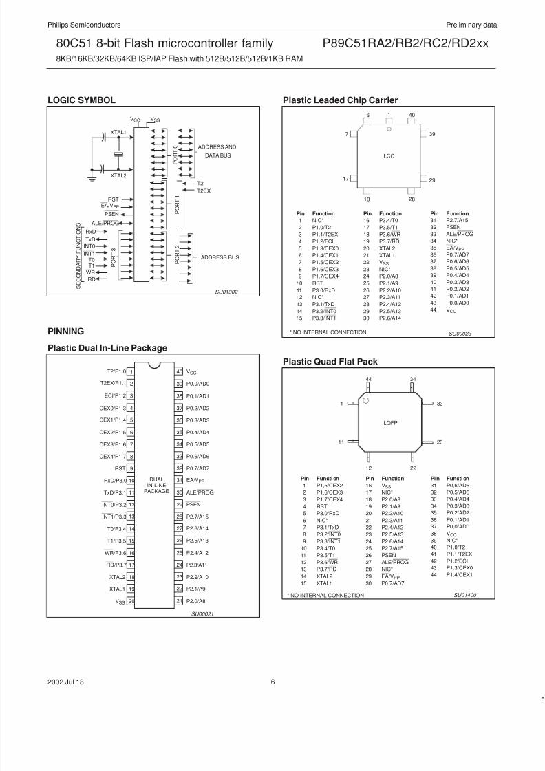
LOGIC SYMBOL
P O R T 0
P O R T 1
P O R T 2
P O R T 3
ADDRESS AND
DATA BUS
ADDRESS BUS
T2
T2EX
RxD
TxD
INT0
INT1T0T1
WR
RD
S E C O N D A R Y F U N C T I O N S
RSTEA/VPP
PSEN
ALE/PROG
VSSVCC
XTAL1
XTAL2
SU01302
PINNING
Plastic Dual In-Line Package
1
2
3
4
5
6
7
8
9
10
11
12
13
14
15
16
17
18
19
20 21
22
23
24
25
26
27
28
29
30
31
32
33
34
35
36
37
38
39
40T2/P1.0
T2EX/P1.1
ECI/P1.2
CEX0/P1.3
CEX1/P1.4
CEX2/P1.5
CEX3/P1.6
RST
RxD/P3.0
TxD/P3.1
INT0/P3.2
INT1/P3.3
T0/P3.4
T1/P3.5
CEX4/P1.7
WR/P3.6
RD/P3.7
XTAL2
XTAL1
VSS P2.0/A8
P2.1/A9
P2.2/A10
P2.3/A11
P2.4/A12
P2.5/A13
P2.6/A14
P2.7/A15
PSEN
ALE/PROG
EA/VPP
P0.7/AD7
P0.6/AD6
P0.5/AD5
P0.4/AD4
P0.3/AD3
P0.2/AD2
P0.1/AD1
P0.0/AD0
VCC
DUALIN-LINE
PACKAGE
SU00021
Plastic Leaded Chip Carrier
LCC
6 1 40
7
17
39
29
18 28
Pin Function
1 NIC*
2 P1.0/T2
3 P1.1/T2EX
4 P1.2/ECI
5 P1.3/CEX0
6 P1.4/CEX1
7 P1.5/CEX2
8 P1.6/CEX39 P1.7/CEX4
10 RST
11 P3.0/RxD
12 NIC*
13 P3.1/TxD
14 P3.2/INT0
15 P3.3/INT1
Pin Function
16 P3.4/T0
17 P3.5/T1
18 P3.6/WR
19 P3.7/RD
20 XTAL2
21 XTAL1
22 VSS
23 NIC*24 P2.0/A8
25 P2.1/A9
26 P2.2/A10
27 P2.3/A11
28 P2.4/A12
29 P2.5/A13
30 P2.6/A14
Pin Function
31 P2.7/A15
32 PSEN
33 ALE/PROG
34 NIC*
35 EA/VPP
36 P0.7/AD7
37 P0.6/AD6
38 P0.5/AD539 P0.4/AD4
40 P0.3/AD3
41 P0.2/AD2
42 P0.1/AD1
43 P0.0/AD0
44 VCC
SU00023 * NO INTERNAL CONNECTION
Plastic Quad Flat Pack
LQFP
44 34
1
11
33
23
12 22
Pin Function
1 P1.5/CEX2
2 P1.6/CEX3
3 P1.7/CEX4
4 RST
5 P3.0/RxD
6 NIC*
7 P3.1/TxD
8 P3.2/INT0
9 P3.3/INT110 P3.4/T0
11 P3.5/T1
12 P3.6/WR
13 P3.7/RD
14 XTAL2
15 XTAL1
Pin Function
16 VSS
17 NIC*
18 P2.0/A8
19 P2.1/A9
20 P2.2/A10
21 P2.3/A11
22 P2.4/A12
23 P2.5/A13
24 P2.6/A1425 P2.7/A15
26 PSEN
27 ALE/PROG
28 NIC*
29 EA/VPP
30 P0.7/AD7
Pin Function
31 P0.6/AD6
32 P0.5/AD5
33 P0.4/AD4
34 P0.3/AD3
35 P0.2/AD2
36 P0.1/AD1
37 P0.0/AD0
38 VCC
39 NIC*40 P1.0/T2
41 P1.1/T2EX
42 P1.2/ECI
43 P1.3/CEX0
44 P1.4/CEX1
SU01400 * NO INTERNAL CONNECTION

8/6/2019 Datasheet p89c51
http://slidepdf.com/reader/full/datasheet-p89c51 7/68
Philips Semiconductors Preliminary data
P89C51RA2/RB2/RC2/RD2xx80C51 8-bit Flash microcontroller family8KB/16KB/32KB/64KB ISP/IAP Flash with 512B/512B/512B/1KB RAM
2002 Jul 18 7
PIN DESCRIPTIONS
PIN NUMBER
PDIP PLCC LQFP
VSS 20 22 16 I Ground: 0 V reference.
VCC 40 44 38 I Power Supply: This is the power supply voltage for normal, idle, and power-downoperation.
P0.0–0.7 39–32 43–36 37–30 I/O Port 0: Port 0 is an open-drain, bidirectional I/O port. Port 0 pins that have 1swritten to them float and can be used as high-impedance inputs. Port 0 is also themultiplexed low-order address and data bus during accesses to external programand data memory. In this application, it uses strong internal pull-ups when emitting 1s.
P1.0–P1.7 1–8 2–9 40–44,1–3
I/O Port 1: Port 1 is an 8-bit bidirectional I/O port with internal pull-ups on all pins.Port 1 pins that have 1s written to them are pulled high by the internal pull-ups andcan be used as inputs. As inputs, port 1 pins that are externally pulled low willsource current because of the internal pull-ups. (See DC Electrical Characteristics:IIL).
Alternate functions for P89C51RA2/RB2/RC2/RD2xx Port 1 include:
1 2 40 I/O T2 (P1.0): Timer/Counter 2 external count input/Clockout (see Programmable
Clock-Out)2 3 41 I T2EX (P1.1): Timer/Counter 2 Reload/Capture/Direction Control
3 4 42 I ECI (P1.2): External Clock Input to the PCA
4 5 43 I/O CEX0 (P1.3): Capture/Compare External I/O for PCA module 0
5 6 44 I/O CEX1 (P1.4): Capture/Compare External I/O for PCA module 1
6 7 1 I/O CEX2 (P1.5): Capture/Compare External I/O for PCA module 2
7 8 2 I/O CEX3 (P1.6): Capture/Compare External I/O for PCA module 3
8 9 3 I/O CEX4 (P1.7): Capture/Compare External I/O for PCA module 4
P2.0–P2.7 21–28 24–31 18–25 I/O Port 2: Port 2 is an 8-bit bidirectional I/O port with internal pull-ups. Port 2 pins thathave 1s written to them are pulled high by the internal pull-ups and can be used asinputs. As inputs, port 2 pins that are externally being pulled low will source currentbecause of the internal pull-ups. (See DC Electrical Characteristics: IIL). Port 2emits the high-order address byte during fetches from external program memoryand during accesses to external data memory that use 16-bit addresses (MOVX
@DPTR). In this application, it uses strong internal pull-ups when emitting 1s.During accesses to external data memory that use 8-bit addresses (MOV @Ri),port 2 emits the contents of the P2 special function register.
P3.0–P3.7 10–17 11,13–19
5, 7–13 I/O Port 3: Port 3 is an 8-bit bidirectional I/O port with internal pull-ups. Port 3 pins thathave 1s written to them are pulled high by the internal pull-ups and can be used asinputs. As inputs, port 3 pins that are externally being pulled low will source currentbecause of the pull-ups. (See DC Electrical Characteristics: I IL). Port 3 also servesthe special features of the P89C51RA2/RB2/RC2/RD2xx, as listed below:
10 11 5 I RxD (P3.0): Serial input port
11 13 7 O TxD (P3.1): Serial output port
12 14 8 I INT0 (P3.2): External interrupt
13 15 9 I INT1 (P3.3): External interrupt
14 16 10 I T0 (P3.4): Timer 0 external input
15 17 11 I T1 (P3.5): Timer 1 external input
16 18 12 O WR (P3.6): External data memory write strobe
17 19 13 O RD (P3.7): External data memory read strobe
RST 9 10 4 I Reset: A high on this pin for two machine cycles while the oscillator is running,resets the device. An internal resistor to VSS permits a power-on reset using onlyan external capacitor to VCC.
ALE 30 33 27 O Address Latch Enable: Output pulse for latching the low byte of the addressduring an access to external memory. In normal operation, ALE is emitted twiceevery machine cycle, and can be used for external timing or clocking. Note that oneALE pulse is skipped during each access to external data memory. ALE can bedisabled by setting SFR auxiliary.0. With this bit set, ALE will be active only during aMOVX instruction.

8/6/2019 Datasheet p89c51
http://slidepdf.com/reader/full/datasheet-p89c51 8/68
Philips Semiconductors Preliminary data
P89C51RA2/RB2/RC2/RD2xx80C51 8-bit Flash microcontroller family8KB/16KB/32KB/64KB ISP/IAP Flash with 512B/512B/512B/1KB RAM
2002 Jul 18 8
MNEMONIC NAME AND FUNCTIONTYPEPIN NUMBER
MNEMONIC NAME AND FUNCTIONTYPELQFPPLCCPDIP
PSEN 29 32 26 O Program Store Enable: The read strobe to external program memory. When
executing code from the external program memory, PSEN is activated twice eachmachine cycle, except that two PSEN activations are skipped during each accessto external data memory. PSEN is not activated during fetches from internalprogram memory.
EA/VPP 31 35 29 I External Access Enable/Programming Supply Voltage: EA must be externallyheld low to enable the device to fetch code from external program memorylocations. If EA is held high, the device executes from internal program memory.The value on the EA pin is latched when RST is released and any subsequentchanges have no effect. This pin also receives the programming supply voltage(VPP) during Flash programming.
XTAL1 19 21 15 I Crystal 1: Input to the inverting oscillator amplifier and input to the internal clockgenerator circuits.
XTAL2 18 20 14 O Crystal 2: Output from the inverting oscillator amplifier.
NOTE:To avoid “latch-up” effect at power-on, the voltage on any pin (other than V
PP) must not be higher than V
CC+ 0.5 V or less than V
SS– 0.5 V.

8/6/2019 Datasheet p89c51
http://slidepdf.com/reader/full/datasheet-p89c51 9/68
Philips Semiconductors Preliminary data
P89C51RA2/RB2/RC2/RD2xx80C51 8-bit Flash microcontroller family8KB/16KB/32KB/64KB ISP/IAP Flash with 512B/512B/512B/1KB RAM
2002 Jul 18 9
Table 1. Special Function Registers
SYMBOL DESCRIPTIONDIRECT
ADDRESS
BIT ADDRESS, SYMBOL, OR ALTERNATIVE PORT FUNCTION
MSB LSB
RESETVALUE
ACC* Accumulator E0H E7 E6 E5 E4 E3 E2 E1 E0 00H
AUXR# Auxiliary 8EH – – – – – – EXTRAM AO xxxxxx00B
AUXR1# Auxiliary 1 A2H – – ENBOOT – GF2 0 – DPS xxxxxxx0B
B* B register F0H F7 F6 F5 F4 F3 F2 F1 F0 00H
CCAP0H# Module 0 Capture High FAH xxxxxxxxB
CCAP1H# Module 1 Capture High FBH xxxxxxxxB
CCAP2H# Module 2 Capture High FCH xxxxxxxxB
CCAP3H# Module 3 Capture High FDH xxxxxxxxB
CCAP4H# Module 4 Capture High FEH xxxxxxxxB
CCAP0L# Module 0 Capture Low EAH xxxxxxxxB
CCAP1L# Module 1 Capture Low EBH xxxxxxxxB
CCAP2L# Module 2 Capture Low ECH xxxxxxxxB
CCAP3L# Module 3 Capture Low EDH xxxxxxxxB
CCAP4L# Module 4 Capture Low EEH xxxxxxxxB
CCAPM0# Module 0 Mode DAH – ECOM CAPP CAPN MAT TOG PWM ECCF x0000000B
CCAPM1# Module 1 Mode DBH – ECOM CAPP CAPN MAT TOG PWM ECCF x0000000B
CCAPM2# Module 2 Mode DCH – ECOM CAPP CAPN MAT TOG PWM ECCF x0000000B
CCAPM3# Module 3 Mode DDH – ECOM CAPP CAPN MAT TOG PWM ECCF x0000000B
CCAPM4# Module 4 Mode DEH – ECOM CAPP CAPN MAT TOG PWM ECCF x0000000B
DF DE DD DC DB DA D9 D8
CCON*# PCA Counter Control D8H CF CR – CCF4 CCF3 CCF2 CCF1 CCF0 00x00000B
CH# PCA Counter High F9H 00H
CKCON# Clock control 8FH – WDX2 PCAX2 SIX2 T2X2 T1X2 T0X2 X2 x0000000B
CL# PCA Counter Low E9H 00H
CMOD# PCA Counter Mode D9H CIDL WDTE – – – CPS1 CPS0 ECF 00xxx000B
DPTR: Data Pointer (2 bytes)
DPH Data Pointer High 83H 00H
DPL Data Pointer Low 82H 00H
AF AE AD AC AB AA A9 A8
IE* Interrupt Enable 0 A8H EA EC ET2 ES ET1 EX1 ET0 EX0 00H
BF BE BD BC BB BA B9 B8
IP* Interrupt Priority B8H – PPC PT2 PS PT1 PX1 PT0 PX0 x0000000B
IPH# Interrupt Priority High B7H – PPCH PT2H PSH PT1H PX1H PT0H PX0H x0000000B
87 86 85 84 83 82 81 80
P0* Port 0 80H AD7 AD6 AD5 AD4 AD3 AD2 AD1 AD0 FFH
97 96 95 94 93 92 91 90
P1* Port 1 90H CEX4 CEX3 CEX2 CEX1 CEX0 ECI T2EX T2 FFH
A7 A6 A5 A4 A3 A2 A1 A0
P2* Port 2 A0H AD15 AD14 AD13 AD12 AD11 AD10 AD9 AD8 FFH
B7 B6 B5 B4 B3 B2 B1 B0
P3* Port 3 B0H RD WR T1 T0 INT1 INT0 TxD RxD FFH
PCON#1 Power Control 87H SMOD1 SMOD0 – POF GF1 GF0 PD IDL 00xxx000B
* SFRs are bit addressable.# SFRs are modified from or added to the 80C51 SFRs. – Reserved bits.1. Reset value depends on reset source.

8/6/2019 Datasheet p89c51
http://slidepdf.com/reader/full/datasheet-p89c51 10/68
Philips Semiconductors Preliminary data
P89C51RA2/RB2/RC2/RD2xx80C51 8-bit Flash microcontroller family8KB/16KB/32KB/64KB ISP/IAP Flash with 512B/512B/512B/1KB RAM
2002 Jul 18 10
Table 1. Special Function Registers (Continued)
SYMBOL DESCRIPTIONDIRECT
ADDRESS
BIT ADDRESS, SYMBOL, OR ALTERNATIVE PORT FUNCTION
MSB LSB
RESETVALUE
D7 D6 D5 D4 D3 D2 D1 D0
PSW* Program Status Word D0H CY AC F0 RS1 RS0 OV F1 P 00000000B
RCAP2H# Timer 2 Capture High CBH 00H
RCAP2L# Timer 2 Capture Low CAH 00H
SADDR# Slave Address A9H 00H
SADEN# Slave Address Mask B9H 00H
SBUF Serial Data Buffer 99H xxxxxxxxB
9F 9E 9D 9C 9B 9A 99 98
SCON* Serial Control 98H SM0/FE SM1 SM2 REN TB8 RB8 TI RI 00H
SP Stack Pointer 81H 07H
8F 8E 8D 8C 8B 8A 89 88
TCON* Timer Control 88H TF1 TR1 TF0 TR0 IE1 IT1 IE0 IT0 00H
CF CE CD CC CB CA C9 C8
T2CON* Timer 2 Control C8H TF2 EXF2 RCLK TCLK EXEN2 TR2 C/T2 CP/RL2 00H
T2MOD# Timer 2 Mode Control C9H – – – – – – T2OE DCEN xxxxxx00B
TH0 Timer High 0 8CH 00H
TH1 Timer High 1 8DH 00H
TH2# Timer High 2 CDH 00H
TL0 Timer Low 0 8AH 00H
TL1 Timer Low 1 8BH 00H
TL2# Timer Low 2 CCH 00H
TMOD Timer Mode 89H GATE C/T M1 M0 GATE C/T M1 M0 00H
WDTRST Watchdog Timer Reset A6H
* SFRs are bit addressable.# SFRs are modified from or added to the 80C51 SFRs. – Reserved bits.
OSCILLATOR CHARACTERISTICSXTAL1 and XTAL2 are the input and output, respectively, of aninverting amplifier. The pins can be configured for use as anon-chip oscillator.
To drive the device from an external clock source, XTAL1 should bedriven while XTAL2 is left unconnected. Minimum and maximumhigh and low times specified in the data sheet must be observed.
This device is configured at the factory to operate using 12 clockperiods per machine cycle, referred to in this datasheet as “12-clockmode”. It may be optionally configured on commercially availableFlash programming equipment or via ISP or via software to operateat 6 clocks per machine cycle, referred to in this datasheet as“6-clock mode”. (This yields performance equivalent to twice that ofstandard 80C51 family devices). Also see next page.

8/6/2019 Datasheet p89c51
http://slidepdf.com/reader/full/datasheet-p89c51 11/68
Philips Semiconductors Preliminary data
P89C51RA2/RB2/RC2/RD2xx80C51 8-bit Flash microcontroller family8KB/16KB/32KB/64KB ISP/IAP Flash with 512B/512B/512B/1KB RAM
2002 Jul 18 11
CLOCK CONTROL REGISTER (CKCON)This device provides control of the 6-clock/12-clock mode by means
of both an SFR bit (X2) and a Flash bit (FX2, located in the Security
Block). The Flash clock control bit, FX2, when programmed (6-clock
mode) supercedes the X2 bit (CKCON.0).
The CKCON register also provides individual control of the clock
rates for the peripherals devices. When running in 6-clock mode
each peripheral may be individually clocked from either fosc/6 or
fosc/12. When in 12-clock mode, all peripheral devices will use
fosc/12. The CKCON register is shown below.
X2
BIT SYMBOL FUNCTION
CKCON.7 – Reserved.
CKCON.6 WDX2 Watchdog clock; 0 = 6 clocks for each WDT clock, 1 = 12 clocks for each WDT clock
CKCON.5 PCAX2 PCA clock; 0 = 6 clocks for each PCA clock, 1 = 12 clocks for each PCA clock
CKCON.4 SIX2 UART clock; 0 = 6 clocks for each UART clock, 1 = 12 clocks for each UART clock
CKCON.3 T2X2 Timer2 clock; 0 = 6 clocks for each Timer2 clock, 1 = 12 clocks for each Timer2 clock
CKCON.2 T1X2 Timer1 clock; 0 = 6 clocks for each Timer1 clock, 1 = 12 clocks for each Timer1 clock
CKCON.1 T0X2 Timer0 clock; 0 = 6 clocks for each Timer0 clock, 1 = 12 clocks for each Timer0 clock
CKCON.0 X2 CPU clock; 1 = 6 clocks for each machine cycle, 0 = 12 clocks for each machine cycle
SU01607
T0X2T1X2T2X2SIX2PCAX2WDX2 –
Not Bit Addressable
CKCON Address = 8Fh Reset Value = x0000000B
7 6 5 4 3 2 1 0
Bits 1 through 6 only apply if 6 clocks per machine cycle is chosen
(i.e.– Bit 0 = 1). If Bit 0 = 0 (12 clocks per machine cycle) then all
peripherals will have 12 clocks per machine cycle as their clock
source.
Also please note that the clock divider applies to the serial port for
modes 0 & 2 (fixed baud rate modes). This is because modes 1 & 3
(variable baud rate modes) use either Timer 1 or Timer 2.
Below is the truth table for the peripheral input clock sources.
FX2 clock mode bit X2 Peripheral clockmode bit
(e.g., T0X2)
CPU MODE Peripheral Clock Rate
erased 0 x 12-clock (default) 12-clock (default)
erased 1 0 6-clock 6-clock
erased 1 1 6-clock 12-clock
programmed x 0 6-clock 6-clock
programmed x 1 6-clock 12-clock
RESETA reset is accomplished by holding the RST pin high for at least two
machine cycles (12 oscillator periods in 6-clock mode, or 24 oscillator
periods in 12-clock mode), while the oscillator is running. To ensure a
good power-on reset, the RST pin must be high long enough to allow
the oscillator time to start up (normally a few milliseconds) plus two
machine cycles. At power-on, the voltage on VCC and RST must
come up at the same time for a proper start-up. Ports 1, 2, and 3 will
asynchronously be driven to their reset condition when a voltage
above VIH1 (min.) is applied to RST.
The value on the EA pin is latched when RST is deasserted and has
no further effect.

8/6/2019 Datasheet p89c51
http://slidepdf.com/reader/full/datasheet-p89c51 12/68
Philips Semiconductors Preliminary data
P89C51RA2/RB2/RC2/RD2xx80C51 8-bit Flash microcontroller family8KB/16KB/32KB/64KB ISP/IAP Flash with 512B/512B/512B/1KB RAM
2002 Jul 18 12
LOW POWER MODESStop Clock ModeThe static design enables the clock speed to be reduced down to
0 MHz (stopped). When the oscillator is stopped, the RAM and
Special Function Registers retain their values. This mode allows
step-by-step utilization and permits reduced system power
consumption by lowering the clock frequency down to any value. For
lowest power consumption the Power Down mode is suggested.
Idle ModeIn the idle mode (see Table 2), the CPU puts itself to sleep while all
of the on-chip peripherals stay active. The instruction to invoke the
idle mode is the last instruction executed in the normal operating
mode before the idle mode is activated. The CPU contents, the
on-chip RAM, and all of the special function registers remain intact
during this mode. The idle mode can be terminated either by any
enabled interrupt (at which time the process is picked up at the
interrupt service routine and continued), or by a hardware reset
which starts the processor in the same manner as a power-on reset.
Power-Down ModeTo save even more power, a Power Down mode (see Table 2) can
be invoked by software. In this mode, the oscillator is stopped and
the instruction that invoked Power Down is the last instruction
executed. The on-chip RAM and Special Function Registers retain
their values down to 2 V and care must be taken to return VCC to the
minimum specified operating voltages before the Power Down Mode
is terminated.
Either a hardware reset or external interrupt can be used to exit f rom
Power Down. Reset redefines all the SFRs but does not change the
on-chip RAM. An external interrupt allows both the SFRs and the
on-chip RAM to retain their values.
To properly terminate Power Down, the reset or external interrupt
should not be executed before VCC is restored to its normal
operating level and must be held active long enough for theoscillator to restart and stabilize (normally less than 10 ms).
With an external interrupt, INT0 and INT1 must be enabled and
configured as level-sensitive. Holding the pin low restarts the oscillator
but bringing the pin back high completes the exit. Once the interrupt
is serviced, the next instruction to be executed after RETI will be the
one following the instruction that put the device into Power Down.
POWER-ON FLAGThe Power-On Flag (POF) is set by on-chip circuitry when the VCC
level on the P89C51RA2/RB2/RC2/RD2xx rises from 0 to 5 V. The
POF bit can be set or cleared by software allowing a user to
determine if the reset is the result of a power-on or a warm start
after powerdown. The VCC level must remain above 3 V for the POF
to remain unaffected by the VCC level.
Design ConsiderationWhen the idle mode is terminated by a hardware reset, the device
normally resumes program execution, from where it left off, up to
two machine cycles before the internal reset algorithm takes control.
On-chip hardware inhibits access to internal RAM in this event, but
access to the port pins is not inhibited. To eliminate the possibility of
an unexpected write when Idle is terminated by reset, the instruction
following the one that invokes Idle should not be one that writes to a
port pin or to external memory.
ONCE™ ModeThe ONCE (“On-Circuit Emulation”) Mode facilitates testing and
debugging of systems without the device having to be removed from
the circuit. The ONCE Mode is invoked by:
1. Pull ALE low while the device is in reset and PSEN is high;
2. Hold ALE low as RST is deactivated.
While the device is in ONCE Mode, the Port 0 pins go into a float
state, and the other port pins and ALE and PSEN are weakly pulledhigh. The oscillator circuit remains active. While the device is in thismode, an emulator or test CPU can be used to drive the circuit.Normal operation is restored when a normal reset is applied.
Programmable Clock-OutA 50% duty cycle clock can be programmed to come out on P1.0.
This pin, besides being a regular I/O pin, has two alternate
functions. It can be programmed:
1. to input the external clock for Timer/Counter 2, or
2. to output a 50% duty cycle clock ranging from 61 Hz to 4 MHz at a
16 MHz operating frequency in 12-clock mode (122 Hz to 8 MHz in
6-clock mode).
To configure the Timer/Counter 2 as a clock generator, bit C/T2 (in
T2CON) must be cleared and bit T20E in T2MOD must be set. Bit
TR2 (T2CON.2) also must be set to start the timer.The Clock-Out frequency depends on the oscillator frequency and
the reload value of Timer 2 capture registers (RCAP2H, RCAP2L)
as shown in this equation:
Oscillator Frequency
n (65536*RCAP2H,RCAP2L)
n = 2 in 6-clock mode4 in 12-clock mode
Where (RCAP2H,RCAP2L) = the content of RCAP2H and RCAP2L
taken as a 16-bit unsigned integer.
In the Clock-Out mode Timer 2 roll-overs will not generate an
interrupt. This is similar to when it is used as a baud-rate generator.
It is possible to use Timer 2 as a baud-rate generator and a clock
generator simultaneously. Note, however, that the baud-rate and theClock-Out frequency will be the same.
Table 2. External Pin Status During Idle and Power-Down Mode
MODE PROGRAM MEMORY ALE PSEN PORT 0 PORT 1 PORT 2 PORT 3
Idle Internal 1 1 Data Data Data Data
Idle External 1 1 Float Data Address Data
Power-down Internal 0 0 Data Data Data Data
Power-down External 0 0 Float Data Data Data

8/6/2019 Datasheet p89c51
http://slidepdf.com/reader/full/datasheet-p89c51 13/68
Philips Semiconductors Preliminary data
P89C51RA2/RB2/RC2/RD2xx80C51 8-bit Flash microcontroller family8KB/16KB/32KB/64KB ISP/IAP Flash with 512B/512B/512B/1KB RAM
2002 Jul 18 13
TIMER 0 AND TIMER 1 OPERATION
Timer 0 and Timer 1The “Timer” or “Counter” function is selected by control bits C/T in
the Special Function Register TMOD. These two Timer/Countershave four operating modes, which are selected by bit-pairs (M1, M0)
in TMOD. Modes 0, 1, and 2 are the same for both Timers/Counters.
Mode 3 is different. The four operating modes are described in the
following text.
Mode 0
Putting either Timer into Mode 0 makes it look like an 8048 Timer,
which is an 8-bit Counter with a divide-by-32 prescaler. Figure 2
shows the Mode 0 operation.
In this mode, the Timer register is configured as a 13-bit register. As
the count rolls over from all 1s to all 0s, it sets the Timer interrupt
flag TFn. The counted input is enabled to the Timer when TRn = 1
and either GATE = 0 or INTn = 1. (Setting GATE = 1 allows the
Timer to be controlled by external input INTn, to facilitate pulse width
measurements). TRn is a control bit in the Special Function RegisterTCON (Figure 3).
The 13-bit register consists of all 8 bits of THn and the lower 5 bits
of TLn. The upper 3 bits of TLn are indeterminate and should be
ignored. Setting the run flag (TRn) does not clear the registers.
Mode 0 operation is the same for Timer 0 as for Timer 1. There are
two different GATE bits, one for Timer 1 (TMOD.7) and one for Timer
0 (TMOD.3).
Mode 1
Mode 1 is the same as Mode 0, except that the Timer register is
being run with all 16 bits.
Mode 2Mode 2 configures the Timer register as an 8-bit Counter (TLn) with
automatic reload, as shown in Figure 4. Overflow from TLn not only
sets TFn, but also reloads TLn with the contents of THn, which is
preset by software. The reload leaves THn unchanged.
Mode 2 operation is the same for Timer 0 as for Timer 1.
Mode 3
Timer 1 in Mode 3 simply holds its count. The effect is the same as
setting TR1 = 0.
Timer 0 in Mode 3 establishes TL0 and TH0 as two separate
counters. The logic for Mode 3 on Timer 0 is shown in Figure 5. TL0
uses the Timer 0 control bits: C/T, GATE, TR0, and TF0 as well as
pin INT0. TH0 is locked into a timer function (counting machine
cycles) and takes over the use of TR1 and TF1 from Timer 1. Thus,
TH0 now controls the “Timer 1” interrupt.
Mode 3 is provided for applications requiring an extra 8-bit timer on
the counter. With Timer 0 in Mode 3, an 80C51 can look like it has
three Timer/Counters. When Timer 0 is in Mode 3, Timer 1 can be
turned on and off by switching it out of and into its own Mode 3, or
can still be used by the serial port as a baud rate generator, or in
fact, in any application not requiring an interrupt.
GATE C/T M1 M0 GATE C/T M1 M0
BIT SYMBOL FUNCTION
TMOD.3/ GATE Gating control when set. Timer/Counter “n” is enabled only while “INTn” pin is high andTMOD.7 “TRn” control pin is set. when cleared Timer “n” is enabled whenever “TRn” control bit is set.
TMOD.2/ C/T Timer or Counter Selector cleared for Timer operation (input from internal system clock.)TMOD.6 Set for Counter operation (input from “Tn” input pin).
M1 M0 OPERATING
0 0 8048 Timer: “TLn” serves as 5-bit prescaler.
0 1 16-bit Timer/Counter: “THn” and “TLn” are cascaded; there is no prescaler.
1 0 8-bit auto-reload Timer/Counter: “THn” holds a value which is to be reloadedinto “TLn” each time it overflows.
1 1 (Timer 0) TL0 is an 8-bit Timer/Counter controlled by the standard Timer 0 control bits.TH0 is an 8-bit timer only controlled by Timer 1 control bits.
1 1 (Timer 1) Timer/Counter 1 stopped.
SU01580
TIMER 1 TIMER 0
Not Bit Addressable
TMOD Address = 89H Reset Value = 00H
7 6 5 4 3 2 1 0
Figure 1. Timer/Counter 0/1 Mode Control (TMOD) Register

8/6/2019 Datasheet p89c51
http://slidepdf.com/reader/full/datasheet-p89c51 14/68
Philips Semiconductors Preliminary data
P89C51RA2/RB2/RC2/RD2xx80C51 8-bit Flash microcontroller family8KB/16KB/32KB/64KB ISP/IAP Flash with 512B/512B/512B/1KB RAM
2002 Jul 18 14
INTn Pin
Timer nGate bit
TRn
TLn(5 Bits)
THn(8 Bits) TFn Interrupt
Control
C/T = 0
C/T = 1
SU01618
OSC ÷ d*
Tn Pin
*d = 6 in 6-clock mode; d = 12 in 12-clock mode.
Figure 2. Timer/Counter 0/1 Mode 0: 13-Bit Timer/Counter
IT0
BIT SYMBOL FUNCTION
TCON.7 TF1 Timer 1 overflow flag. Set by hardware on Timer/Counter overflow.Cleared by hardware when processor vectors to interrupt routine, or clearing the bit in software.
TCON.6 TR1 Timer 1 Run control bit. Set/cleared by software to turn Timer/Counter on/off.TCON.5 TF0 Timer 0 overflow flag. Set by hardware on Timer/Counter overflow.
Cleared by hardware when processor vectors to interrupt routine, or by clearing the bit in software.
TCON.4 TR0 Timer 0 Run control bit. Set/cleared by software to turn Timer/Counter on/off.
TCON.3 IE1 Interrupt 1 Edge flag. Set by hardware when external interrupt edge detected.Cleared when interrupt processed.
TCON.2 IT1 Interrupt 1 type control bit. Set/cleared by software to specify falling edge/low level triggeredexternal interrupts.
TCON.1 IE0 Interrupt 0 Edge flag. Set by hardware when external interrupt edge detected.Cleared when interrupt processed.
TCON.0 IT0 Interrupt 0 Type control bit. Set/cleared by software to specify falling edge/low leveltriggered external interrupts.
SU01516
IE0IT1IE1TR0TF0TR1TF1
Bit Addressable
TCON Address = 88H Reset Value = 00H
7 6 5 4 3 2 1 0
Figure 3. Timer/Counter 0/1 Control (TCON) Register

8/6/2019 Datasheet p89c51
http://slidepdf.com/reader/full/datasheet-p89c51 15/68
Philips Semiconductors Preliminary data
P89C51RA2/RB2/RC2/RD2xx80C51 8-bit Flash microcontroller family8KB/16KB/32KB/64KB ISP/IAP Flash with 512B/512B/512B/1KB RAM
2002 Jul 18 15
TLn(8 Bits) TFn Interrupt
Control
C/T = 0
C/T = 1
THn(8 Bits)
Reload
INTn Pin
Timer nGate bit
TRn
SU01619
OSC ÷ d*
Tn Pin
*d = 6 in 6-clock mode; d = 12 in 12-clock mode.
Figure 4. Timer/Counter 0/1 Mode 2: 8-Bit Auto-Reload
TL0(8 Bits) TF0 Interrupt
Control
TH0(8 Bits) TF1 Interrupt
Control
TR1
INT0 Pin
Timer 0Gate bit
TR0
SU01620
C/T = 0
C/T = 1
*d = 6 in 6-clock mode; d = 12 in 12-clock mode.
OSC ÷ d*
OSC ÷ d*
T0 Pin
Figure 5. Timer/Counter 0 Mode 3: Two 8-Bit Counters

8/6/2019 Datasheet p89c51
http://slidepdf.com/reader/full/datasheet-p89c51 16/68
Philips Semiconductors Preliminary data
P89C51RA2/RB2/RC2/RD2xx80C51 8-bit Flash microcontroller family8KB/16KB/32KB/64KB ISP/IAP Flash with 512B/512B/512B/1KB RAM
2002 Jul 18 16
TIMER 2 OPERATION
Timer 2Timer 2 is a 16-bit Timer/Counter which can operate as either an
event timer or an event counter, as selected by C/T2 in the specialfunction register T2CON (see Figure 6). Timer 2 has three operating
modes: Capture, Auto-reload (up or down counting), and Baud RateGenerator, which are selected by bits in the T2CON as shown in
Table 3.
Capture ModeIn the capture mode there are two options which are selected by bit
EXEN2 in T2CON. If EXEN2=0, then timer 2 is a 16-bit timer orcounter (as selected by C/T2 in T2CON) which, upon overflowing
sets bit TF2, the timer 2 overflow bit. This bit can be used togenerate an interrupt (by enabling the Timer 2 interrupt bit in the
IE register). If EXEN2= 1, Timer 2 operates as described above, but
with the added feature that a 1- to -0 transition at external input
T2EX causes the current value in the Timer 2 registers, TL2 andTH2, to be captured into registers RCAP2L and RCAP2H,
respectively. In addition, the transition at T2EX causes bit EXF2 inT2CON to be set, and EXF2 like TF2 can generate an interrupt
(which vectors to the same location as Timer 2 overflow interrupt.The Timer 2 interrupt service routine can interrogate TF2 and EXF2
to determine which event caused the interrupt). The capture mode isillustrated in Figure 7 (There is no reload value for TL2 and TH2 in
this mode. Even when a capture event occurs from T2EX, the
counter keeps on counting T2EX pin transitions or osc/6 pulses
(osc/12 in 12-clock mode).).
Auto-Reload Mode (Up or Down Counter)In the 16-bit auto-reload mode, Timer 2 can be configured (as eithera timer or counter [C/T2 in T2CON]) then programmed to count up
or down. The counting direction is determined by bit DCEN (Down
Counter Enable) which is located in the T2MOD register (see
Figure 8). When reset is applied the DCEN=0 which means Timer 2
will default to counting up. If DCEN bit is set, Timer 2 can count upor down depending on the value of the T2EX pin.
Figure 9 shows Timer 2 which will count up automatically since
DCEN=0. In this mode there are two options selected by bit EXEN2
in T2CON register. If EXEN2=0, then Timer 2 counts up to 0FFFFH
and sets the TF2 (Overflow Flag) bit upon overflow. This causes the
Timer 2 registers to be reloaded with the 16-bit value in RCAP2L
and RCAP2H. The values in RCAP2L and RCAP2H are preset by
software means.
If EXEN2=1, then a 16-bit reload can be triggered either by an
overflow or by a 1-to-0 transition at input T2EX. This transition also
sets the EXF2 bit. The Timer 2 interrupt, if enabled, can be
generated when either TF2 or EXF2 are 1.
In Figure 10 DCEN=1 which enables Timer 2 to count up or down.
This mode allows pin T2EX to control the direction of count. When a
logic 1 is applied at pin T2EX Timer 2 will count up. Timer 2 will
overflow at 0FFFFH and set the TF2 flag, which can then generatean interrupt, if the interrupt is enabled. This timer overflow also
causes the 16-bit value in RCAP2L and RCAP2H to be reloaded
into the timer registers TL2 and TH2.
When a logic 0 is applied at pin T2EX this causes Timer 2 to count
down. The timer will underflow when TL2 and TH2 become equal to
the value stored in RCAP2L and RCAP2H. Timer 2 underflow sets
the TF2 flag and causes 0FFFFH to be reloaded into the timer
registers TL2 and TH2.
The external flag EXF2 toggles when Timer 2 underflows or overflows.
This EXF2 bit can be used as a 17th bit of resolution if needed. The
EXF2 flag does not generate an interrupt in this mode of operation.
(MSB) (LSB)
Symbol Position Name and Significance
TF2 T2CON.7 Timer 2 overflow flag set by a Timer 2 overflow and must be cleared by software. TF2 will not be setwhen either RCLK or TCLK = 1.
EXF2 T2CON.6 Timer 2 external flag set when either a capture or reload is caused by a negative transition on T2EX andEXEN2 = 1. When Timer 2 interrupt is enabled, EXF2 = 1 will cause the CPU to vector to the Timer 2interrupt routine. EXF2 must be cleared by software. EXF2 does not cause an interrupt in up/downcounter mode (DCEN = 1).
RCLK T2CON.5 Receive clock flag. When set, causes the serial port to use Timer 2 overflow pulses for its receive clockin modes 1 and 3. RCLK = 0 causes Timer 1 overflow to be used for the receive clock.
TCLK T2CON.4 Transmit clock flag. When set, causes the serial port to use Timer 2 overflow pulses for its transmit clock
in modes 1 and 3. TCLK = 0 causes Timer 1 overflows to be used for the transmit clock.EXEN2 T2CON.3 Timer 2 external enable flag. When set, allows a capture or reload to occur as a result of a negative
transition on T2EX if Timer 2 is not being used to clock the serial port. EXEN2 = 0 causes Timer 2 toignore events at T2EX.
TR2 T2CON.2 Start/stop control for Timer 2. A logic 1 starts the timer.
C/T2 T2CON.1 Timer or counter select. (Timer 2)0 = Internal timer (OSC/6 in 6-clock mode or OSC/12 in 12-clock mode)1 = External event counter (falling edge triggered).
CP/RL2 T2CON.0 Capture/Reload flag. When set, captures will occur on negative transitions at T2EX if EXEN2 = 1. Whencleared, auto-reloads will occur either with Timer 2 overflows or negative transitions at T2EX whenEXEN2 = 1. When either RCLK = 1 or TCLK = 1, this bit is ignored and the timer is forced to auto-reloadon Timer 2 overflow.
TF2 EXF2 RCLK TCLK EXEN2 TR2 C/T2 CP/RL2
SU01251
Figure 6. Timer/Counter 2 (T2CON) Control Register

8/6/2019 Datasheet p89c51
http://slidepdf.com/reader/full/datasheet-p89c51 17/68
Philips Semiconductors Preliminary data
P89C51RA2/RB2/RC2/RD2xx80C51 8-bit Flash microcontroller family8KB/16KB/32KB/64KB ISP/IAP Flash with 512B/512B/512B/1KB RAM
2002 Jul 18 17
Table 3. Timer 2 Operating Modes
RCLK + TCLK CP/RL2 TR2 MODE
0 0 1 16-bit Auto-reload
0 1 1 16-bit Capture
1 X 1 Baud rate generator
X X 0 (off)
OSC ÷ n*
C/T2 = 0
C/T2 = 1
TR2
Control
TL2(8 BITS)
TH2(8 BITS)
TF2
RCAP2L RCAP2H
EXEN2
Control
EXF2
Timer 2Interrupt
T2EX Pin
TransitionDetector
T2 Pin
Capture
SU01252
* n = 6 in 6-clock mode, or 12 in 12-clock mode.
Figure 7. Timer 2 in Capture Mode
Not Bit Addressable
Symbol Function
— Not implemented, reserved for future use.*
T2OE Timer 2 Output Enable bit.
DCEN Down Count Enable bit. When set, this allows Timer 2 to be configured as an up/down counter.
— — — — — — T2OE DCEN
SU00729
7 6 5 4 3 2 1 0
* User software should not write 1s to reserved bits. These bits may be used in future 8051 family products to invoke new features.In that case, the reset or inactive value of the new bit will be 0, and its active value will be 1. The value read from a reserved bit isindeterminate.
Bit
T2MOD Address = 0C9H Reset Value = XXXX XX00B
Figure 8. Timer 2 Mode (T2MOD) Control Register

8/6/2019 Datasheet p89c51
http://slidepdf.com/reader/full/datasheet-p89c51 18/68
Philips Semiconductors Preliminary data
P89C51RA2/RB2/RC2/RD2xx80C51 8-bit Flash microcontroller family8KB/16KB/32KB/64KB ISP/IAP Flash with 512B/512B/512B/1KB RAM
2002 Jul 18 18
OSC ÷ n*
C/T2 = 0
C/T2 = 1
TR2
CONTROL
TL2
(8 BITS)
TH2
(8 BITS)
TF2RCAP2L RCAP2H
EXEN2
CONTROL
EXF2
TIMER 2INTERRUPT
T2EX PIN
TRANSITIONDETECTOR
T2 PIN
RELOAD
SU01253
* n = 6 in 6-clock mode, or 12 in 12-clock mode.
Figure 9. Timer 2 in Auto-Reload Mode (DCEN = 0)
÷ n* C/T2 = 0
C/T2 = 1
TL2 TH2
TR2
CONTROL
T2 PIN
SU01254
FFH FFH
RCAP2L RCAP2H
(UP COUNTING RELOAD VALUE) T2EX PIN
TF2 INTERRUPT
COUNTDIRECTION1 = UP0 = DOWN
EXF2
OVERFLOW
(DOWN COUNTING RELOAD VALUE)
TOGGLE
OSC
* n = 6 in 6-clock mode, or 12 in 12-clock mode.
Figure 10. Timer 2 Auto Reload Mode (DCEN = 1)

8/6/2019 Datasheet p89c51
http://slidepdf.com/reader/full/datasheet-p89c51 19/68
Philips Semiconductors Preliminary data
P89C51RA2/RB2/RC2/RD2xx80C51 8-bit Flash microcontroller family8KB/16KB/32KB/64KB ISP/IAP Flash with 512B/512B/512B/1KB RAM
2002 Jul 18 19
C/T2 = 0
C/T2 = 1
TR2
Control
TL2(8-bits)
TH2(8-bits)
÷ 16
RCAP2L RCAP2H
EXEN2
Control
EXF2 Timer 2Interrupt
T2EX Pin
TransitionDetector
Reload
÷ 2
“0” “1”
RX Clock
÷ 16 TX Clock
“0”“1”
“0”“1”
Timer 1Overflow
Note availability of additional external interrupt.
SMOD
RCLK
TCLK
SU01629
n = 1 in 6-clock moden = 2 in 12-clock mode
OSC ÷ n
T2 Pin
Figure 11. Timer 2 in Baud Rate Generator Mode
Table 4. Timer 2 Generated Commonly UsedBaud Rates
Baud Rate Timer 212-clock
mode6-clockmode
Osc FreqRCAP2H RCAP2L
375 k 750 k 12 MHz FF FF
9.6 k 19.2 k 12 MHz FF D9
4.8 k 9.6 k 12 MHz FF B2
2.4 k 4.8 k 12 MHz FF 64
1.2 k 2.4 k 12 MHz FE C8
300 600 12 MHz FB 1E
110 220 12 MHz F2 AF
300 600 6 MHz FD 8F
110 220 6 MHz F9 57
Baud Rate Generator Mode
Bits TCLK and/or RCLK in T2CON (Table 4) allow the serial porttransmit and receive baud rates to be derived from either Timer 1 or
Timer 2. When TCLK= 0, Timer 1 is used as the serial port transmit
baud rate generator. When TCLK= 1, Timer 2 is used as the serial
port transmit baud rate generator. RCLK has the same effect for the
serial port receive baud rate. With these two bits, the serial port can
have different receive and transmit baud rates – one generated by
Timer 1, the other by Timer 2.
Figure 11 shows the Timer 2 in baud rate generation mode. The baud
rate generation mode is like the auto-reload mode,in that a rollover in
TH2 causes the Timer 2 registers to be reloaded with the 16-bit value
in registers RCAP2H and RCAP2L, which are preset by software.
The baud rates in modes 1 and 3 are determined by Timer 2’s
overflow rate given below:
Modes 1 and 3 Baud Rates +Timer 2 Overflow Rate
16The timer can be configured for either “timer” or “counter” operation.In many applications, it is configured for “timer” operation (C/T2=0).
Timer operation is different for Timer 2 when it is being used as a
baud rate generator.
Usually, as a t imer it would increment every machine cycle (i.e.,1 / 6 the oscillator frequency in 6-clock mode, 1 / 12 the oscillator
frequency in 12-clock mode). As a baud rate generator, it
increments at the oscillator frequency in 6-clock mode (OSC / 2 in12-clock mode). Thus the baud rate formula is as follows:
Oscillator Frequency
[ n * [65536* (RCAP2H,RCAP2L)]]
Modes 1 and 3 Baud Rates =
* n = 16 in 6-clock mode32 in 12-clock mode
Where: (RCAP2H, RCAP2L)= The content of RCAP2H andRCAP2L taken as a 16-bit unsigned integer.
The Timer 2 as a baud rate generator mode shown in Figure 11, is
valid only if RCLK and/or TCLK = 1 in T2CON register. Note that arollover in TH2 does not set TF2, and will not generate an interrupt.
Thus, the Timer 2 interrupt does not have to be disabled whenTimer 2 is in the baud rate generator mode. Also if the EXEN2
(T2 external enable flag) is set, a 1-to-0 transition in T2EX
(Timer/counter 2 trigger input) will set EXF2 (T2 external flag) but
will not cause a reload from (RCAP2H, RCAP2L) to (TH2,TL2).Therefore when Timer 2 is in use as a baud rate generator, T2EX
can be used as an additional external interrupt, if needed.
8/6/2019 Datasheet p89c51
http://slidepdf.com/reader/full/datasheet-p89c51 20/68
Philips Semiconductors Preliminary data
P89C51RA2/RB2/RC2/RD2xx80C51 8-bit Flash microcontroller family8KB/16KB/32KB/64KB ISP/IAP Flash with 512B/512B/512B/1KB RAM
2002 Jul 18 20
When Timer 2 is in the baud rate generator mode, one should not try
to read or write TH2 and TL2. As a baud rate generator, Timer 2 is
incremented every state time (osc/2) or asynchronously from pin T2;
under these conditions, a read or write of TH2 or TL2 may not be
accurate. The RCAP2 registers may be read, but should not bewritten to, because a write might overlap a reload and cause write
and/or reload errors. The timer should be turned off (clear TR2)
before accessing the Timer 2 or RCAP2 registers.
Table 4 shows commonly used baud rates and how they can be
obtained from Timer 2.
Summary of Baud Rate EquationsTimer 2 is in baud rate generating mode. If Timer 2 is being clocked
through pin T2 (P1.0) the baud rate is:
Baud Rate + Timer 2 Overflow Rate16
If Timer 2 is being clocked internally, the baud rate is:
Baud Rate+fOSC
[ n * [65536* (RCAP2H,RCAP2L)]]
* n = 16 in 6-clock mode32 in 12-clock mode
Where fOSC= Oscillator Frequency
To obtain the reload value for RCAP2H and RCAP2L, the above
equation can be rewritten as:
RCAP2H,RCAP2L+ 65536* fOSC
n * Baud Rate
Timer/Counter 2 Set-upExcept for the baud rate generator mode, the values given for T2CON
do not include the setting of the TR2 bit. Therefore, bit TR2 must be
set, separately, to turn the timer on. see Table 5 for set-up of Timer 2
as a timer. Also see Table 6 for set-up of Timer 2 as a counter.
Table 5. Timer 2 as a Timer
T2CON
MODE INTERNAL CONTROL(Note 1)
EXTERNAL CONTROL(Note 2)
16-bit Auto-Reload 00H 08H
16-bit Capture 01H 09H
Baud rate generator receive and transmit same baud rate 34H 36H
Receive only 24H 26H
Transmit only 14H 16H
Table 6. Timer 2 as a Counter
TMOD
MODE INTERNAL CONTROL(Note 1)
EXTERNAL CONTROL(Note 2)
16-bit 02H 0AH
Auto-Reload 03H 0BH
NOTES:1. Capture/reload occurs only on timer/counter overflow.2. Capture/reload occurs on timer/counter overflow and a 1-to-0 transition on T2EX (P1.1) pin except when Timer 2 is used in the baud rate
generator mode.

8/6/2019 Datasheet p89c51
http://slidepdf.com/reader/full/datasheet-p89c51 21/68
Philips Semiconductors Preliminary data
P89C51RA2/RB2/RC2/RD2xx80C51 8-bit Flash microcontroller family8KB/16KB/32KB/64KB ISP/IAP Flash with 512B/512B/512B/1KB RAM
2002 Jul 18 21
FULL-DUPLEX ENHANCED UART
Standard UART operationThe serial port is full duplex, meaning it can transmit and receive
simultaneously. It is also receive-buffered, meaning it cancommence reception of a second byte before a previously received
byte has been read from the register. (However, if the first byte still
hasn’t been read by the time reception of the second byte is
complete, one of the bytes will be lost.) The serial port receive and
transmit registers are both accessed at Special Function Register
SBUF. Writing to SBUF loads the transmit register, and reading
SBUF accesses a physically separate receive register.
The serial port can operate in 4 modes:
Mode 0: Serial data enters and exits through RxD. TxD outputs
the shift clock. 8 bits are transmitted/received (LSB first).
The baud rate is fixed at 1/12 the oscillator frequency in
12-clock mode or 1/6 the oscillator frequency in 6-clock
mode.
Mode 1: 10 bits are transmitted (through TxD) or received
(through RxD): a start bit (0), 8 data bits (LSB first), and
a stop bit (1). On receive, the stop bit goes into RB8 in
Special Function Register SCON. The baud rate is
variable.
Mode 2: 11 bits are transmitted (through TxD) or received
(through RxD): start bit (0), 8 data bits (LSB first), a
programmable 9th data bit, and a stop bit (1). On
Transmit, the 9th data bit (TB8 in SCON) can be
assigned the value of 0 or 1. Or, for example, the parity
bit (P, in the PSW) could be moved into TB8. On receive,
the 9th data bit goes into RB8 in Special Function
Register SCON, while the stop bit is ignored. The baud
rate is programmable to either 1/32 or 1/64 the oscillator
frequency in 12-clock mode or 1/16 or 1/32 the oscillatorfrequency in 6-clock mode.
Mode 3: 11 bits are transmitted (through TxD) or received
(through RxD): a start bit (0), 8 data bits (LSB first), a
programmable 9th data bit, and a stop bit (1). In fact,
Mode 3 is the same as Mode 2 in all respects except
baud rate. The baud rate in Mode 3 is variable.
In all four modes, transmission is initiated by any instruction that
uses SBUF as a destination register. Reception is initiated in Mode 0
by the condition RI = 0 and REN = 1. Reception is initiated in the
other modes by the incoming start bit if REN = 1.
Multiprocessor Communications
Modes 2 and 3 have a special provision for multiprocessor
communications. In these modes, 9 data bits are received. The 9th
one goes into RB8. Then comes a stop bit. The port can beprogrammed such that when the stop bit is received, the serial port
interrupt will be activated only if RB8 = 1. This feature is enabled by
setting bit SM2 in SCON. A way to use this feature in multiprocessor
systems is as follows:
When the master processor wants to transmit a block of data to one
of several slaves, it first sends out an address byte which identifies
the target slave. An address byte differs from a data byte in that the
9th bit is 1 in an address byte and 0 in a data byte. With SM2 = 1, no
slave will be interrupted by a data byte. An address byte, however,
will interrupt all slaves, so that each slave can examine the received
byte and see if it is being addressed. The addressed slave will clear
its SM2 bit and prepare to receive the data bytes that will be coming.
The slaves that weren’t being addressed leave their SM2s set and
go on about their business, ignoring the coming data bytes.
SM2 has no effect in Mode 0, and in Mode 1 can be used to check
the validity of the stop bit. In a Mode 1 reception, if SM2 = 1, thereceive interrupt will not be activated unless a valid stop bit is
received.
Serial Port Control Register
The serial port control and status register is the Special Function
Register SCON, shown in Figure 12. This register contains not only
the mode selection bits, but also the 9th data bit for transmit and
receive (TB8 and RB8), and the serial port interrupt bits (TI and RI).
Baud Rates
The baud rate in Mode 0 is fixed: Mode 0 Baud Rate = Oscillator
Frequency / 12 (12-clock mode) or / 6 (6-clock mode). The baud
rate in Mode 2 depends on the value of bit SMOD in Special
Function Register PCON. If SMOD = 0 (which is the value on reset),
and the port pins in 12-clock mode, the baud rate is 1/64 the
oscillator frequency. If SMOD = 1, the baud rate is 1/32 the oscillatorfrequency. In 6-clock mode, the baud rate is 1/32 or 1/16 the
oscillator frequency, respectively.
Mode 2 Baud Rate =
2SMOD
n (Oscillator Frequency)
Where:
n = 64 in 12-clock mode, 32 in 6-clock mode
The baud rates in Modes 1 and 3 are determined by the Timer 1 or
Timer 2 overflow rate.
Using Timer 1 to Generate Baud Rates
When Timer 1 is used as the baud rate generator (T2CON.RCLK
= 0, T2CON.TCLK = 0), the baud rates in Modes 1 and 3 are
determined by the Timer 1 overflow rate and the value of SMOD asfollows:
Mode 1, 3 Baud Rate =
2SMOD
n (Timer 1 Overflow Rate)
Where:
n = 32 in 12-clock mode, 16 in 6-clock mode
The Timer 1 interrupt should be disabled in this application. The
Timer itself can be configured for either “timer” or “counter”
operation, and in any of its 3 running modes. In the most typical
applications, it is configured for “timer” operation, in the auto-reload
mode (high nibble of TMOD = 0010B). In that case the baud rate is
given by the formula:
Mode 1, 3 Baud Rate =
2SMOD
n Oscillator Frequency
12 [256–(TH1)]
Where:
n = 32 in 12-clock mode, 16 in 6-clock mode
One can achieve very low baud rates with Timer 1 by leaving the
Timer 1 interrupt enabled, and configuring the Timer to run as a
16-bit timer (high nibble of TMOD = 0001B), and using the Timer 1
interrupt to do a 16-bit software reload. Figure 13 lists various
commonly used baud rates and how they can be obtained from
Timer 1.

8/6/2019 Datasheet p89c51
http://slidepdf.com/reader/full/datasheet-p89c51 22/68
Philips Semiconductors Preliminary data
P89C51RA2/RB2/RC2/RD2xx80C51 8-bit Flash microcontroller family8KB/16KB/32KB/64KB ISP/IAP Flash with 512B/512B/512B/1KB RAM
2002 Jul 18 22
SM2 Enables the multiprocessor communication feature in Modes 2 and 3. In Mode 2 or 3, if SM2 is set to 1, then Rl will not beactivated if the received 9th data bit (RB8) is 0. In Mode 1, if SM2=1 then RI will not be activated if a valid stop bit was notreceived. In Mode 0, SM2 should be 0.
REN Enables serial reception. Set by software to enable reception. Clear by software to disable reception.
TB8 The 9th data bit that will be transmitted in Modes 2 and 3. Set or clear by software as desired.
RB8 In Modes 2 and 3, is the 9th data bit that was received. In Mode 1, it SM2=0, RB8 is the stop bit that was received. In Mode 0,
RB8 is not used.TI Transmit interrupt flag. Set by hardware at the end of the 8th bit time in Mode 0, or at the beginning of the stop bit in the other
modes, in any serial transmission. Must be cleared by software.
RI Receive interrupt flag. Set by hardware at the end of the 8th bit time in Mode 0, or halfway through the stop bit time in the othermodes, in any serial reception (except see SM2). Must be cleared by software.
SM0 SM1 SM2 REN TB8 RB8 TI RI
Where SM0, SM1 specify the serial port mode, as follows:
SM0 SM1 Mode Description Baud Rate
0 0 0 shift register fOSC /12 (12-clock mode) or fOSC /6 (6-clock mode)
0 1 1 8-bit UART variable
1 0 2 9-bit UART fOSC /64 or fOSC /32 (12-clock mode) or fOSC /32 or fOSC /16 (6-clock mode)
1 1 3 9-bit UART variable
SU01626
Bit Addressable
SCON Address = 98H Reset Value = 00H
7 6 5 4 3 2 1 0
Figure 12. Serial Port Control (SCON) Register
Baud Rate Timer 1
Mode 12-clock mode 6-clock modeOSC
C/T Mode Reload Value
Mode 0 Max 1.67 MHz 3.34 MHz 20 MHz X X X X
Mode 2 Max 625 k 1250 k 20 MHz 1 X X X
Mode 1, 3 Max 104.2 k 208.4 k 20 MHz 1 0 2 FFH
Mode 1, 3 19.2 k 38.4 k 11.059 MHz 1 0 2 FDH
9.6 k 19.2 k 11.059 MHz 0 0 2 FDH
4.8 k 9.6 k 11.059 MHz 0 0 2 FAH
2.4 k 4.8 k 11.059 MHz 0 0 2 F4H
1.2 k 2.4 k 11.059 MHz 0 0 2 E8H
137.5 275 11.986 MHz 0 0 2 1DH
110 220 6 MHz 0 0 2 72H
110 220 12 MHz 0 0 1 FEEBH
Figure 13. Timer 1 Generated Commonly Used Baud Rates
More About Mode 0
Serial data enters and exits through RxD. TxD outputs the shift
clock. 8 bits are transmitted/received: 8 data bits (LSB first). The
baud rate is fixed a 1/12 the oscillator frequency (12-clock mode) or
1/6 the oscillator frequency (6-clock mode).
Figure 14 shows a simplified functional diagram of the serial port inMode 0, and associated timing.
Transmission is initiated by any instruction that uses SBUF as a
destination register. The “write to SBUF” signal at S6P2 also loads a
1 into the 9th position of the transmit shift register and tells the TXControl block to commence a transmission. The internal timing is
such that one full machine cycle will elapse between “write to SBUF”
and activation of SEND.
SEND enables the output of the shift register to the alternate outputfunction line of P3.0 and also enable SHIFT CLOCK to the alternate
output function line of P3.1. SHIFT CLOCK is low during S3, S4, and
S5 of every machine cycle, and high during S6, S1, and S2. At
S6P2 of every machine cycle in which SEND is active, the contents
of the transmit shift are shifted to the right one position.
As data bits shift out to the right, zeros come in from the left. When
the MSB of the data byte is at the output position of the shift register,then the 1 that was initially loaded into the 9th position, is just to the
left of the MSB, and all positions to the left of that contain zeros.
This condition flags the TX Control block to do one last shift andthen deactivate SEND and set T1. Both of these actions occur at
S1P1 of the 10th machine cycle after “write to SBUF.”
Reception is initiated by the condition REN = 1 and R1 = 0. At S6P2
of the next machine cycle, the RX Control unit writes the bits11111110 to the receive shift register, and in the next clock phase
activates RECEIVE.
RECEIVE enable SHIFT CLOCK to the alternate output function line
of P3.1. SHIFT CLOCK makes transitions at S3P1 and S6P1 ofevery machine cycle. At S6P2 of every machine cycle in which
RECEIVE is active, the contents of the receive shift register are

8/6/2019 Datasheet p89c51
http://slidepdf.com/reader/full/datasheet-p89c51 23/68
Philips Semiconductors Preliminary data
P89C51RA2/RB2/RC2/RD2xx80C51 8-bit Flash microcontroller family8KB/16KB/32KB/64KB ISP/IAP Flash with 512B/512B/512B/1KB RAM
2002 Jul 18 23
shifted to the left one position. The value that comes in from the right
is the value that was sampled at the P3.0 pin at S5P2 of the same
machine cycle.
As data bits come in from the right, 1s shift out to the left. When the
0 that was initially loaded into the rightmost position arrives at the
leftmost position in the shift register, it flags the RX Control block to
do one last shift and load SBUF. At S1P1 of the 10th machine cycle
after the write to SCON that cleared RI, RECEIVE is cleared as RI is
set.
More About Mode 1
Ten bits are transmitted (through TxD), or received (through RxD): a
start bit (0), 8 data bits (LSB first), and a stop bit (1). On receive, the
stop bit goes into RB8 in SCON. In the 80C51 the baud rate is
determined by the Timer 1 or Timer 2 overflow rate.
Figure 15 shows a simplified functional diagram of the serial port inMode 1, and associated timings for transmit receive.
Transmission is initiated by any instruction that uses SBUF as a
destination register. The “write to SBUF” signal also loads a 1 into
the 9th bit position of the transmit shift register and flags the TX
Control unit that a transmission is requested. Transmission actuallycommences at S1P1 of the machine cycle following the next rollover
in the divide-by-16 counter. (Thus, the bit times are synchronized tothe divide-by-16 counter, not to the “write to SBUF” signal.)
The transmission begins with activation of SEND which puts the
start bit at TxD. One bit time later, DATA is activated, which enables
the output bit of the transmit shift register to TxD. The first shift pulseoccurs one bit time after that.
As data bits shift out to the right, zeros are clocked in from the left.
When the MSB of the data byte is at the output position of the shift
register, then the 1 that was initially loaded into the 9th position is
just to the left of the MSB, and all positions to the left of that containzeros. This condition flags the TX Control unit to do one last shift
and then deactivate SEND and set TI. This occurs at the 10thdivide-by-16 rollover after “write to SBUF.”
Reception is initiated by a detected 1-to-0 transition at RxD. For this
purpose RxD is sampled at a rate of 16 times whatever baud ratehas been established. When a transition is detected, the
divide-by-16 counter is immediately reset, and 1FFH is written intothe input shift register. Resetting the divide-by-16 counter aligns its
rollovers with the boundaries of the incoming bit times.
The 16 states of the counter divide each bit time into 16ths. At the
7th, 8th, and 9th counter states of each bit time, the bit detectorsamples the value of RxD. The value accepted is the value that was
seen in at least 2 of the 3 samples. This is done for noise rejection.
If the value accepted during the first bit time is not 0, the receive
circuits are reset and the unit goes back to looking for another 1-to-0transition. This is to provide rejection of false start bits. If the start bit
proves valid, it is shifted into the input shift register, and reception ofthe rest of the frame will proceed.
As data bits come in from the right, 1s shift out to the left. When the
start bit arrives at the leftmost position in the shift register (which inmode 1 is a 9-bit register), it flags the RX Control block to do one
last shift, load SBUF and RB8, and set RI. The signal to load SBUFand RB8, and to set RI, will be generated if, and only if, the following
conditions are met at the time the final shift pulse is generated.:
1. R1 = 0, and
2. Either SM2 = 0, or the received stop bit = 1.
If either of these two conditions is not met, the received frame isirretrievably lost. If both conditions are met, the stop bit goes into
RB8, the 8 data bits go into SBUF, and RI is activated. At this time,
whether the above conditions are met or not, the unit goes back to
looking for a 1-to-0 transition in RxD.
More About Modes 2 and 3
Eleven bits are transmitted (through TxD), or received (through
RxD): a start bit (0), 8 data bits (LSB first), a programmable 9th databit, and a stop bit (1). On transmit, the 9th data bit (TB8) can be
assigned the value of 0 or 1. On receive, the 9the data bit goes into
RB8 in SCON. The baud rate is programmable to either 1/32 or 1/64(12-clock mode) or 1/16 or 1/32 the oscillator frequency (6-clock
mode) the oscillator frequency in Mode 2. Mode 3 may have a
variable baud rate generated from Timer 1 or Timer 2.
Figures 16 and 17 show a functional diagram of the serial port in
Modes 2 and 3. The receive portion is exactly the same as in Mode1. The transmit portion differs from Mode 1 only in the 9th bit of the
transmit shift register.
Transmission is initiated by any instruction that uses SBUF as a
destination register. The “write to SBUF” signal also loads TB8 intothe 9th bit position of the transmit shift register and flags the TX
Control unit that a transmission is requested. Transmissioncommences at S1P1 of the machine cycle following the next rolloverin the divide-by-16 counter. (Thus, the bit times are synchronized to
the divide-by-16 counter, not to the “write to SBUF” signal.)
The transmission begins with activation of SEND, which puts thestart bit at TxD. One bit time later, DATA is activated, which enablesthe output bit of the transmit shift register to TxD. The first shift pulseoccurs one bit time after that. The first shift clocks a 1 (the stop bit)into the 9th bit position of the shift register. Thereafter, only zerosare clocked in. Thus, as data bits shift out to the right, zeros areclocked in from the left. When TB8 is at the output position of theshift register, then the stop bit is just to the left of TB8, and allpositions to the left of that contain zeros. This condition flags the TXControl unit to do one last shift and then deactivate SEND and setTI. This occurs at the 11th divide-by-16 rollover after “write to SUBF.”
Reception is initiated by a detected 1-to-0 transition at RxD. For thispurpose RxD is sampled at a rate of 16 times whatever baud ratehas been established. When a transition is detected, the
divide-by-16 counter is immediately reset, and 1FFH is written to the
input shift register.
At the 7th, 8th, and 9th counter states of each bit time, the bitdetector samples the value of R-D. The value accepted is the value
that was seen in at least 2 of the 3 samples. If the value accepted
during the first bit time is not 0, the receive circuits are reset and the
unit goes back to looking for another 1-to-0 transition. If the start bitproves valid, it is shifted into the input shift register, and reception of
the rest of the frame will proceed.
As data bits come in from the right, 1s shift out to the left. When the
start bit arrives at the leftmost position in the shift register (which inModes 2 and 3 is a 9-bit register), it flags the RX Control block to do
one last shift, load SBUF and RB8, and set RI.
The signal to load SBUF and RB8, and to set RI, will be generated
if, and only if, the following conditions are met at the time the final
shift pulse is generated.
1. RI = 0, and
2. Either SM2 = 0, or the received 9th data bit = 1.
If either of these conditions is not met, the received frame is
irretrievably lost, and RI is not set. If both conditions are met, the
received 9th data bit goes into RB8, and the first 8 data bits go into
SBUF. One bit t ime later, whether the above conditions were met or
not, the unit goes back to looking for a 1-to-0 transition at the RxD
input.

8/6/2019 Datasheet p89c51
http://slidepdf.com/reader/full/datasheet-p89c51 24/68
Philips Semiconductors Preliminary data
P89C51RA2/RB2/RC2/RD2xx80C51 8-bit Flash microcontroller family8KB/16KB/32KB/64KB ISP/IAP Flash with 512B/512B/512B/1KB RAM
2002 Jul 18 24
80C51 Internal Bus
SBUF
Zero Detector
D QS
CL
Writeto
SBUF
TX Control
TX Clock Send
ShiftStart
S6
RX Control
Start
Shift
ReceiveRX Clock
T1
R1
SerialPort
Interrupt
1 1 1 1 1 1 1 0
Input Shift Register
REN
RI
LoadSBUF
Shift
ShiftClock
RxDP3.0 AltOutput
Function
TxDP3.1 AltOutput
Function
SBUF
ReadSBUF
80C51 Internal Bus
RxDP3.0 Alt
InputFunction
Write to SBUF
S6P2Send
Shift
RxD (Data Out) D0 D1 D2 D3 D4 D5 D6 D7
Transmit
TxD (Shift Clock)
TIS3P1 S6P1
Write to SCON (Clear RI)
RI
Receive
Shift
RxD (Data In) D0 D1 D2 D3 D4 D5 D6
TxD (Shift Clock)
S5P2
Receive
D7
ALE
S4 . . S1 S6. . . . S1 S6. . . . S1 S6. . . . S1 S6. . . . S1 S6. . . . S1 S6. . . . S1 S6. . . . S1 S6. . . . S1 S6. . . . S1 S6. . . . S1
SU00539
LSB
LSB MSB
MSB
Figure 14. Serial Port Mode 0

8/6/2019 Datasheet p89c51
http://slidepdf.com/reader/full/datasheet-p89c51 25/68
Philips Semiconductors Preliminary data
P89C51RA2/RB2/RC2/RD2xx80C51 8-bit Flash microcontroller family8KB/16KB/32KB/64KB ISP/IAP Flash with 512B/512B/512B/1KB RAM
2002 Jul 18 25
80C51 Internal Bus
SBUF
Zero Detector
D QS
CL
Writeto
SBUF
TX Control
TX Clock Send
DataStart
RX ControlStart
RX Clock RI
T1
SerialPort
Interrupt
Input Shift Register(9 Bits)
LoadSBUF
Shift
SBUF
ReadSBUF
80C51 Internal Bus
TxD
TB8
÷ 16
1-to-0TransitionDetector
Sample
÷ 2
Timer 1Overflow
SMOD = 1SMOD = 0
Shift
Bit Detector
Transmit
Send
S1P1
Shift
TXClock
Write to SBUF
Start BitTxD Stop BitD0 D1 D2 D3 D4 D5 D6 D7
TI
RxD
RXClock
÷ 16 Reset
StartBitRxD Stop BitD0 D1 D2 D3 D4 D5 D6 D7
Bit DetectorSample Times
Shift
RI
Receive
Data
÷ 16
LoadSBUF
Shift
1FFH
SU00540
Figure 15. Serial Port Mode 1

8/6/2019 Datasheet p89c51
http://slidepdf.com/reader/full/datasheet-p89c51 26/68
Philips Semiconductors Preliminary data
P89C51RA2/RB2/RC2/RD2xx80C51 8-bit Flash microcontroller family8KB/16KB/32KB/64KB ISP/IAP Flash with 512B/512B/512B/1KB RAM
2002 Jul 18 26
80C51 Internal Bus
SBUF
Zero Detector
D QS
CL
Writeto
SBUF
TX Control
TX Clock Send
DataStart
RX ControlStart
LoadSBUF
RX Clock
T1
SerialPort
Interrupt
Input Shift Register(9 Bits)
LoadSBUF
Shift
SBUF
ReadSBUF
80C51 Internal Bus
TxD
TB8
÷ 16
1-to-0TransitionDetector
Sample
÷ 2
SMOD = 1
SMOD = 0
Shift
Bit Detector
RxD
Stop BitGen.
Mode 2
Phase 2 Clock(1/2 fOSC)
R1
÷ 16
Shift
1FFH
Transmit
Send
S1P1
Shift
TXClock
Write to SBUF
Start BitTxD Stop BitD0 D1 D2 D3 D4 D5 D6 D7
TI
RXClock
÷ 16 Reset
StartBit
RxD Stop BitD0 D1 D2 D3 D4 D5 D6 D7Bit DetectorSample Times
Shift
RI
Receive
Data
(SMOD isPCON.7)
TB8
RB8
Stop Bit Gen.
SU00541
Figure 16. Serial Port Mode 2

8/6/2019 Datasheet p89c51
http://slidepdf.com/reader/full/datasheet-p89c51 27/68
Philips Semiconductors Preliminary data
P89C51RA2/RB2/RC2/RD2xx80C51 8-bit Flash microcontroller family8KB/16KB/32KB/64KB ISP/IAP Flash with 512B/512B/512B/1KB RAM
2002 Jul 18 27
80C51 Internal Bus
SBUF
Zero Detector
D QS
CL
Writeto
SBUF
TX Control
TX Clock Send
DataStart
RX ControlStart
RX Clock
T1
SerialPort
Interrupt
Input Shift Register(9 Bits)
LoadSBUF
Shift
SBUF
ReadSBUF
80C51 Internal Bus
TxD
TB8
÷ 16
1-to-0TransitionDetector
Sample
÷ 2
Timer 1Overflow
SMOD = 1SMOD = 0
Shift
Bit Detector
RxD
R1
÷ 16
LoadSBUF
Shift
1FFH
Transmit
Send
S1P1
Shift
TXClock
Write to SBUF
Start BitTxD Stop BitD0 D1 D2 D3 D4 D5 D6 D7
TI
RXClock
÷ 16 Reset
StartBit
RxD Stop BitD0 D1 D2 D3 D4 D5 D6 D7Bit DetectorSample Times
Shift
RI
Receive
Data
TB8
RB8
Stop Bit Gen.
SU00542
Figure 17. Serial Port Mode 3

8/6/2019 Datasheet p89c51
http://slidepdf.com/reader/full/datasheet-p89c51 28/68
Philips Semiconductors Preliminary data
P89C51RA2/RB2/RC2/RD2xx80C51 8-bit Flash microcontroller family8KB/16KB/32KB/64KB ISP/IAP Flash with 512B/512B/512B/1KB RAM
2002 Jul 18 28
Enhanced UARTIn addition to the standard operation the UART can perform framing
error detect by looking for missing stop bits, and automatic address
recognition. The UART also fully supports multiprocessor
communication as does the standard 80C51 UART.
When used for framing error detect the UART looks for missing stop
bits in the communication. A missing bit will set the FE bit in the
SCON register. The FE bit shares the SCON.7 bit with SM0 and the
function of SCON.7 is determined by PCON.6 (SMOD0) (see
Figure 18). If SMOD0 is set then SCON.7 functions as FE. SCON.7
functions as SM0 when SMOD0 is cleared. When used as FE
SCON.7 can only be cleared by software. Refer to Figure 19.
Automatic Address Recognition
Automatic Address Recognition is a feature which allows the UART
to recognize certain addresses in the serial bit stream by using
hardware to make the comparisons. This feature saves a great deal
of software overhead by eliminating the need for the software to
examine every serial address which passes by the serial port. This
feature is enabled by setting the SM2 bit in SCON. In the 9 bit UARTmodes, mode 2 and mode 3, the Receive Interrupt flag (RI) will be
automatically set when the received byte contains either the “Given”
address or the “Broadcast” address. The 9-bit mode requires that
the 9th information bit is a 1 to indicate that the received information
is an address and not data. Automatic address recognition is shown
in Figure 20.
The 8 bit mode is called Mode 1. In this mode the RI flag will be set
if SM2 is enabled and the information received has a valid stop bit
following the 8 address bits and the information is either a Given or
Broadcast address.
Mode 0 is the Shift Register mode and SM2 is ignored.
Using the Automatic Address Recognition feature allows a master to
selectively communicate with one or more slaves by invoking the
Given slave address or addresses. All of the slaves may be
contacted by using the Broadcast address. Two special Function
Registers are used to define the slave’s address, SADDR, and the
address mask, SADEN. SADEN is used to define which bits in the
SADDR are to b used and which bits are “don’t care”. The SADEN
mask can be logically ANDed with the SADDR to create the “Given”
address which the master will use for addressing each of the slaves.
Use of the Given address allows multiple slaves to be recognized
while excluding others. The following examples will help to show the
versatility of this scheme:
Slave 0 SADDR = 1100 0000
SADEN = 1111 1101
Given = 1100 00X0
Slave 1 SADDR = 1100 0000
SADEN = 1111 1110
Given = 1100 000X
In the above example SADDR is the same and the SADEN data is
used to differentiate between the two slaves. Slave 0 requires a 0 in
bit 0 and it ignores bit 1. Slave 1 requires a 0 in bit 1 and bit 0 is
ignored. A unique address for Slave 0 would be 1100 0010 since
slave 1 requires a 0 in bit 1. A unique address for slave 1 would be
1100 0001 since a 1 in bit 0 will exclude slave 0. Both slaves can be
selected at the same time by an address which has bit 0 = 0 (for
slave 0) and bit 1 = 0 (for slave 1). Thus, both could be addressed
with 1100 0000.
In a more complex system the following could be used to select
slaves 1 and 2 while excluding slave 0:
Slave 0 SADDR = 1100 0000
SADEN = 1111 1001
Given = 1100 0XX0
Slave 1 SADDR = 1110 0000SADEN = 1111 1010
Given = 1110 0X0X
Slave 2 SADDR = 1110 0000
SADEN = 1111 1100
Given = 1110 00XX
In the above example the differentiation among the 3 slaves is in the
lower 3 address bits. Slave 0 requires that bit 0 = 0 and it can be
uniquely addressed by 1110 0110. Slave 1 requires that bit 1 = 0 and
it can be uniquely addressed by 1110 and 0101. Slave 2 requires
that bit 2 = 0 and its unique address is 1110 0011. To select Slaves 0
and 1 and exclude Slave 2 use address 1110 0100, since it is
necessary to make bit 2 = 1 to exclude slave 2.
The Broadcast Address for each slave is created by taking the
logical OR of SADDR and SADEN. Zeros in this result are trended
as don’t-cares. In most cases, interpreting the don’t-cares as ones,
the broadcast address will be FF hexadecimal.
Upon reset SADDR (SFR address 0A9H) and SADEN (SFR
address 0B9H) are leaded with 0s. This produces a given address
of all “don’t cares” as well as a Broadcast address of all “don’t
cares”. This effectively disables the Automatic Addressing mode and
allows the microcontroller to use standard 80C51 type UART drivers
which do not make use of this feature.

8/6/2019 Datasheet p89c51
http://slidepdf.com/reader/full/datasheet-p89c51 29/68
Philips Semiconductors Preliminary data
P89C51RA2/RB2/RC2/RD2xx80C51 8-bit Flash microcontroller family8KB/16KB/32KB/64KB ISP/IAP Flash with 512B/512B/512B/1KB RAM
2002 Jul 18 29
SCON Address = 98H Reset Value = 0000 0000B
SM0/FE SM1 SM2 REN TB8 RB8 Tl Rl
Bit Addressable
(SMOD0 = 0/1)*
Symbol Function
FE Framing Error bit. This bit is set by the receiver when an invalid stop bit is detected. The FE bit is not cleared by validframes but should be cleared by software. The SMOD0 bit must be set to enable access to the FE bit.
SM0 Serial Port Mode Bit 0, (SMOD0 must = 0 to access bit SM0)
SM1 Serial Port Mode Bit 1SM0 SM1 Mode Description Baud Rate**
0 0 0 shift register fOSC /6 (6-clock mode) or fOSC /12 (12-clock mode)
0 1 1 8-bit UART variable
1 0 2 9-bit UART fOSC /32 or fOSC /16 (6-clock mode) or
fOSC /64 or fOSC /32 (12-clock mode)
1 1 3 9-bit UART variableSM2 Enables the Automatic Address Recognition feature in Modes 2 or 3. If SM2 = 1 then Rl will not be set unless the
received 9th data bit (RB8) is 1, indicating an address, and the received byte is a Given or Broadcast Address.In Mode 1, if SM2 = 1 then Rl will not be activated unless a valid stop bit was received, and the received byte is aGiven or Broadcast Address. In Mode 0, SM2 should be 0.
REN Enables serial reception. Set by software to enable reception. Clear by software to disable reception.
TB8 The 9th data bit that will be transmitted in Modes 2 and 3. Set or clear by software as desired.
RB8 In modes 2 and 3, the 9th data bit that was received. In Mode 1, if SM2 = 0, RB8 is the stop bit that was received.In Mode 0, RB8 is not used.
Tl Transmit interrupt flag. Set by hardware at the end of the 8th bit time in Mode 0, or at the beginning of the stop bit in theother modes, in any serial transmission. Must be cleared by software.
Rl Receive interrupt flag. Set by hardware at the end of the 8th bit time in Mode 0, or halfway through the stop bit time inthe other modes, in any serial reception (except see SM2). Must be cleared by software.
NOTE:
*SMOD0 is located at PCON6.
**fOSC = oscillator frequency SU01255
Bit: 7 6 5 4 3 2 1 0
Figure 18. SCON: Serial Port Control Register

8/6/2019 Datasheet p89c51
http://slidepdf.com/reader/full/datasheet-p89c51 30/68
Philips Semiconductors Preliminary data
P89C51RA2/RB2/RC2/RD2xx80C51 8-bit Flash microcontroller family8KB/16KB/32KB/64KB ISP/IAP Flash with 512B/512B/512B/1KB RAM
2002 Jul 18 30
SMOD1 SMOD0 – POF LVF GF0 GF1 IDLPCON(87H)
SM0 / FE SM1 SM2 REN TB8 RB8 TI RISCON(98H)
D0 D1 D2 D3 D4 D5 D6 D7 D8
STOPBIT
DATA BYTE ONLY INMODE 2, 3
STARTBIT
SET FE BIT IF STOP BIT IS 0 (FRAMING ERROR)
SM0 TO UART MODE CONTROL
0 : SCON.7 = SM01 : SCON.7 = FE
SU00044
Figure 19. UART Framing Error Detection
SM0 SM1 SM2 REN TB8 RB8 TI RISCON(98H)
D0 D1 D2 D3 D4 D5 D6 D7 D8
11
10
COMPARATOR
1 1 X
RECEIVED ADDRESS D0 TO D7
PROGRAMMED ADDRESS
IN UART MODE 2 OR MODE 3 AND SM2 = 1:INTERRUPT IF REN=1, RB8=1 AND “RECEIVED ADDRESS” = “PROGRAMMED ADDRESS”
– WHEN OWN ADDRESS RECEIVED, CLEAR SM2 TO RECEIVE DATA BYTES – WHEN ALL DATA BYTES HAVE BEEN RECEIVED: SET SM2 TO WAIT FOR NEXT ADDRESS.
SU00045
Figure 20. UART Multiprocessor Communication, Automatic Address Recognition

8/6/2019 Datasheet p89c51
http://slidepdf.com/reader/full/datasheet-p89c51 31/68
Philips Semiconductors Preliminary data
P89C51RA2/RB2/RC2/RD2xx80C51 8-bit Flash microcontroller family8KB/16KB/32KB/64KB ISP/IAP Flash with 512B/512B/512B/1KB RAM
2002 Jul 18 31
Interrupt Priority StructureThe P89C51RA2/RB2/RC2/RD2xx has a 7 source four-level
interrupt structure (see Table 7).
There are 3 SFRs associated with the four-level interrupt. They arethe IE, IP, and IPH. (See Figures 21, 22, and 23.) The IPH (Interrupt
Priority High) register makes the four-level interrupt structure
possible. The IPH is located at SFR address B7H. The structure of
the IPH register and a description of its bits is shown in Figure 23.
The function of the IPH SFR, when combined with the IP SFR,
determines the priority of each interrupt. The priority of each
interrupt is determined as shown in the following table:
PRIORITY BITS
IPH.x IP.x
0 0 Level 0 (lowest priority)
0 1 Level 1
1 0 Level 21 1 Level 3 (highest priority)
The priority scheme for servicing the interrupts is the same as that
for the 80C51, except there are four interrupt levels rather than two
as on the 80C51. An interrupt will be serviced as long as an interrupt
of equal or higher priority is not already being serviced. If an
interrupt of equal or higher level priority is being serviced, the newinterrupt will wait until it is finished before being serviced. If a lower
priority level interrupt is being serviced, it will be stopped and the
new interrupt serviced. When the new interrupt is finished, the lower
priority level interrupt that was stopped will be completed.
Table 7. Interrupt Table
SOURCE POLLING PRIORITY REQUEST BITS HARDWARE CLEAR? VECTOR ADDRESS
X0 1 IE0 N (L)1 Y (T)2 03H
T0 2 TP0 Y 0BH
X1 3 IE1 N (L) Y (T) 13H
T1 4 TF1 Y 1BH
PCA 5 CF, CCFnn = 0–4
N 33H
SP 6 RI, TI N 23H
T2 7 TF2, EXF2 N 2BH
NOTES:1. L = Level activated2. T = Transition activated
EX0IE (0A8H)
Enable Bit = 1 enables the interrupt.Enable Bit = 0 disables it.
BIT SYMBOL FUNCTIONIE.7 EA Global disable bit. If EA = 0, all interrupts are disabled. If EA = 1, each interrupt can be individually
enabled or disabled by setting or clearing its enable bit.IE.6 EC PCA interrupt enable bit
IE.5 ET2 Timer 2 interrupt enable bit.
IE.4 ES Serial Port interrupt enable bit.
IE.3 ET1 Timer 1 interrupt enable bit.
IE.2 EX1 External interrupt 1 enable bit.
IE.1 ET0 Timer 0 interrupt enable bit.
IE.0 EX0 External interrupt 0 enable bit.SU01290
ET0EX1ET1ESET2ECEA
01234567
Figure 21. IE Registers
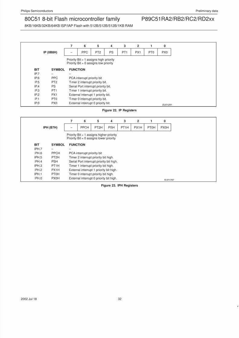
8/6/2019 Datasheet p89c51
http://slidepdf.com/reader/full/datasheet-p89c51 32/68
Philips Semiconductors Preliminary data
P89C51RA2/RB2/RC2/RD2xx80C51 8-bit Flash microcontroller family8KB/16KB/32KB/64KB ISP/IAP Flash with 512B/512B/512B/1KB RAM
2002 Jul 18 32
PX0IP (0B8H)
Priority Bit = 1 assigns high priorityPriority Bit = 0 assigns low priority
BIT SYMBOL FUNCTION
IP.7 – –
IP.6 PPC PCA interrupt priority bit
IP.5 PT2 Timer 2 interrupt priority bit.
IP.4 PS Serial Port interrupt priority bit.
IP.3 PT1 Timer 1 interrupt priority bit.
IP.2 PX1 External interrupt 1 priority bit.
IP.1 PT0 Timer 0 interrupt priority bit.
IP.0 PX0 External interrupt 0 priority bit.SU01291
PT0PX1PT1PSPT2PPC –
01234567
Figure 22. IP Registers
PX0HIPH (B7H)
Priority Bit = 1 assigns higher priorityPriority Bit = 0 assigns lower priority
BIT SYMBOL FUNCTION
IPH.7 – –
IPH.6 PPCH PCA interrupt priority bit
IPH.5 PT2H Timer 2 interrupt priority bit high.
IPH.4 PSH Serial Port interrupt priority bit high.
IPH.3 PT1H Timer 1 interrupt priority bit high.
IPH.2 PX1H External interrupt 1 priority bit high.
IPH.1 PT0H Timer 0 interrupt priority bit high.
IPH.0 PX0H External interrupt 0 priority bit high. SU01292
PT0HPX1HPT1HPSHPT2HPPCH –
01234567
Figure 23. IPH Registers

8/6/2019 Datasheet p89c51
http://slidepdf.com/reader/full/datasheet-p89c51 33/68
Philips Semiconductors Preliminary data
P89C51RA2/RB2/RC2/RD2xx80C51 8-bit Flash microcontroller family8KB/16KB/32KB/64KB ISP/IAP Flash with 512B/512B/512B/1KB RAM
2002 Jul 18 33
Reduced EMI ModeThe AO bit (AUXR.0) in the AUXR register when set disables the
ALE output unless the CPU needs to perform an off-chip memory
access.
Reduced EMI Mode
AUXR (8EH)
7 6 5 4 3 2 1 0
– – – – – – EXTRAM AO
AUXR.1 EXTRAM
AUXR.0 AO
See more detailed description in Figure 38.
Dual DPTRThe dual DPTR structure (see Figure 24) is a way by which the chip
will specify the address of an external data memory location. There
are two 16-bit DPTR registers that address the external memory,
and a single bit called DPS = AUXR1/bit0 that allows the programcode to switch between them.
• New Register Name: AUXR1#
• SFR Address: A2H
• Reset Value: xxxxxxx0B
AUXR1 (A2H)
7 6 5 4 3 2 1 0
– – ENBOOT – GF2 0 – DPS
Where:
DPS = AUXR1/bit0 = Switches between DPTR0 and DPTR1.
Select Reg DPS
DPTR0 0
DPTR1 1
The DPS bit status should be saved by software when switching
between DPTR0 and DPTR1.
The GF2 bit is a general purpose user-defined flag. Note that bit 2 is
not writable and is always read as a zero. This allows the DPS bit to
be quickly toggled simply by executing an INC AUXR1 instruction
without affecting the GF2 bit.
The ENBOOT bit determines whether the BOOTROM is enabled
or disabled. This bit will automatically be set if the status byte is
non zero during reset or PSEN is pulled low, ALE floats high, and
EA > VIH on the falling edge of reset. Otherwise, this bit will be
cleared during reset.
DPS
DPTR1
DPTR0
DPH(83H)
DPL(82H) EXTERNAL
DATAMEMORY
SU00745A
BIT0AUXR1
Figure 24.
DPTR Instructions
The instructions that refer to DPTR refer to the data pointer that is
currently selected using the AUXR1/bit 0 register. The six
instructions that use the DPTR are as follows:
INC DPTR Increments the data pointer by 1
MOV DPTR, #data16 Loads the DPTR with a 16-bit constant
MOV A, @ A+DPTR Move code byte relative to DPTR to ACC
MOVX A, @ DPTR Move external RAM (16-bit address) toACC
MOVX @ DPTR , A Move ACC to external RAM (16-bitaddress)
JMP @ A + DPTR Jump indirect relative to DPTR
The data pointer can be accessed on a byte-by-byte basis by
specifying the low or high byte in an instruction which accesses the
SFRs. See Application Note AN458 for more details.

8/6/2019 Datasheet p89c51
http://slidepdf.com/reader/full/datasheet-p89c51 34/68
Philips Semiconductors Preliminary data
P89C51RA2/RB2/RC2/RD2xx80C51 8-bit Flash microcontroller family8KB/16KB/32KB/64KB ISP/IAP Flash with 512B/512B/512B/1KB RAM
2002 Jul 18 34
Programmable Counter Array (PCA)The Programmable Counter Array available on the
P89C51RA2/RB2/RC2/RD2xx is a special 16-bit Timer that has five
16-bit capture/compare modules associated with it. Each of the
modules can be programmed to operate in one of four modes: risingand/or falling edge capture, software timer, high-speed output, or
pulse width modulator. Each module has a pin associated with it in
port 1. Module 0 is connected to P1.3 (CEX0), module 1 to P1.4
(CEX1), etc. The basic PCA configuration is shown in Figure 25.
The PCA timer is a common time base for all five modules and can
be programmed to run at: 1/6 the oscillator frequency, 1/2 the
oscillator frequency, the Timer 0 overflow, or the input on the ECI pin
(P1.2). The timer count source is determined from the CPS1 and
CPS0 bits in the CMOD SFR as follows (see Figure 28):
CPS1 CPS0 PCA Timer Count Source
0 0 1/6 oscillator frequency (6-clock mode);
1/12 oscillator frequency (12-clock mode)
0 1 1/2 oscillator frequency (6-clock mode);
1/4 oscillator frequency (12-clock mode)1 0 Timer 0 overflow
1 1 External Input at ECI pin
In the CMOD SFR are three additional bits associated with the PCA.
They are CIDL which allows the PCA to stop during idle mode,
WDTE which enables or disables the watchdog function on
module 4, and ECF which when set causes an interrupt and the
PCA overflow flag CF (in the CCON SFR) to be set when the PCA
timer overflows. These functions are shown in Figure 26.
The watchdog timer function is implemented in module 4 (see
Figure 35).
The CCON SFR contains the run control bit for the PCA and the
flags for the PCA timer (CF) and each module (refer to Figure 29).
To run the PCA the CR bit (CCON.6) must be set by software. The
PCA is shut off by clearing this bit. The CF bit (CCON.7) is set when
the PCA counter overflows and an interrupt will be generated if the
ECF bit in the CMOD register is set, The CF bit can only be cleared
by software. Bits 0 through 4 of the CCON register are the flags for
the modules (bit 0 for module 0, bit 1 for module 1, etc.) and are set
by hardware when either a match or a capture occurs. These flagsalso can only be cleared by software. The PCA interrupt system
shown in Figure 27.
Each module in the PCA has a special function register associated
with it. These registers are: CCAPM0 for module 0, CCAPM1 for
module 1, etc. (see Figure 30). The registers contain the bits that
control the mode that each module will operate in. The ECCF bit
(CCAPMn.0 where n=0, 1, 2, 3, or 4 depending on the module)
enables the CCF flag in the CCON SFR to generate an interrupt
when a match or compare occurs in the associated module. PWM
(CCAPMn.1) enables the pulse width modulation mode. The TOG
bit (CCAPMn.2) when set causes the CEX output associated with
the module to toggle when there is a match between the PCA
counter and the module’s capture/compare register. The match bit
MAT (CCAPMn.3) when set will cause the CCFn bit in the CCON
register to be set when there is a match between the PCA counterand the module’s capture/compare register.
The next two bits CAPN (CCAPMn.4) and CAPP (CCAPMn.5)
determine the edge that a capture input will be active on. The CAPN
bit enables the negative edge, and the CAPP bit enables the positive
edge. If both bits are set both edges will be enabled and a capture will
occur for either transition. The last bit in the register ECOM
(CCAPMn.6) when set enables the comparator function. Figure 31
shows the CCAPMn settings for the various PCA functions.
There are two additional registers associated with each of the PCA
modules. They are CCAPnH and CCAPnL and these are the
registers that store the 16-bit count when a capture occurs or a
compare should occur. When a module is used in the PWM mode
these registers are used to control the duty cycle of the output.
MODULE FUNCTIONS:
16-BIT CAPTURE
16-BIT TIMER
16-BIT HIGH SPEED OUTPUT
8-BIT PWM
WATCHDOG TIMER (MODULE 4 ONLY)
MODULE 0
MODULE 1
MODULE 2
MODULE 3
MODULE 4
P1.3/CEX0
P1.4/CEX1
P1.5/CEX2
P1.6/CEX3
P1.7/CEX4
16 BITS
PCA TIMER/COUNTER
TIME BASE FOR PCA MODULES
16 BITS
SU00032
Figure 25. Programmable Counter Array (PCA)

8/6/2019 Datasheet p89c51
http://slidepdf.com/reader/full/datasheet-p89c51 35/68
Philips Semiconductors Preliminary data
P89C51RA2/RB2/RC2/RD2xx80C51 8-bit Flash microcontroller family8KB/16KB/32KB/64KB ISP/IAP Flash with 512B/512B/512B/1KB RAM
2002 Jul 18 35
CF CR CCF4 CCF3 CCF2 CCF1 CCF0 –– CCON(C0H)
CH CL
OVERFLOW
INTERRUPT
16–BIT UP COUNTER
IDLE
TO PCAMODULES
CMOD(C1H)
CIDL WDTE –– –– –– CPS1 CPS0 ECF
OSC/6 (6 CLOCK MODE)OR
OSC/12 (12 CLOCK MODE)
TIMER 0 OVERFLOW
EXTERNAL INPUT(P1.2/ECI)
DECODE
00011011
SU01256
OSC/2 (6 CLOCK MODE)OR
OSC/4 (12 CLOCK MODE)
Figure 26. PCA Timer/Counter
MODULE 0
MODULE 1
MODULE 2
MODULE 3
MODULE 4
PCA TIMER/COUNTER
CF CR CCF4 CCF3 CCF2 CCF1 CCF0 ––
CMOD.0 ECF CCAPMn.0 ECCFn
TOINTERRUPTPRIORITYDECODER
CCON(C0H)
IE.6EC
IE.7EA
SU01097
Figure 27. PCA Interrupt System

8/6/2019 Datasheet p89c51
http://slidepdf.com/reader/full/datasheet-p89c51 36/68
Philips Semiconductors Preliminary data
P89C51RA2/RB2/RC2/RD2xx80C51 8-bit Flash microcontroller family8KB/16KB/32KB/64KB ISP/IAP Flash with 512B/512B/512B/1KB RAM
2002 Jul 18 36
CMOD Address = D9H Reset Value = 00XX X000B
CIDL WDTE – – – CPS1 CPS0 ECF
Bit:
Symbol Function
CIDL Counter Idle control: CIDL = 0 programs the PCA Counter to continue functioning during idle Mode. CIDL = 1 programsit to be gated off during idle.
WDTE Watchdog Timer Enable: WDTE = 0 disables Watchdog Timer function on PCA Module 4. WDTE = 1 enables it.
– Not implemented, reserved for future use.*
CPS1 PCA Count Pulse Select bit 1.
CPS0 PCA Count Pulse Select bit 0.CPS1 CPS0 Selected PCA Input**
0 0 0 Internal clock, fOSC /6 in 6-clock mode (fOSC /12 in 12-clock mode)0 1 1 Internal clock, fOSC /2 in 6-clock mode (fOSC /4 in 12-clock mode)
1 0 2 Timer 0 overflow
1 1 3 External clock at ECI/P1.2 pin
(max. rate = fOSC /4 in 6-clock mode, fOCS /8 in 12-clock mode)
ECF PCA Enable Counter Overflow interrupt: ECF = 1 enables CF bit in CCON to generate an interrupt. ECF = 0 disablesthat function of CF.
NOTE:* User software should not write 1s to reserved bits. These bits may be used in future 8051 family products to invoke new features. In that case, the reset or inactive
value of the new bit will be 0, and its active value will be 1. The value read from a reserved bit is indeterminate.
** fOSC = oscillator frequency
SU01318
7 6 5 4 3 2 1 0
Figure 28. CMOD: PCA Counter Mode Register
CCON Address = D8H Reset Value = 00X0 0000B
CF CR – CCF4 CCF3 CCF2 CCF1 CCF0
Bit Addressable
Bit:
Symbol Function
CF PCA Counter Overflow flag. Set by hardware when the counter rolls over. CF flags an interrupt if bit ECF in CMOD isset. CF may be set by either hardware or software but can only be cleared by software.
CR PCA Counter Run control bit. Set by software to turn the PCA counter on. Must be cleared by software to turn the PCAcounter off.
– Not implemented, reserved for future use*.
CCF4 PCA Module 4 interrupt flag. Set by hardware when a match or capture occurs. Must be cleared by software.
CCF3 PCA Module 3 interrupt flag. Set by hardware when a match or capture occurs. Must be cleared by software.
CCF2 PCA Module 2 interrupt flag. Set by hardware when a match or capture occurs. Must be cleared by software.
CCF1 PCA Module 1 interrupt flag. Set by hardware when a match or capture occurs. Must be cleared by software.
CCF0 PCA Module 0 interrupt flag. Set by hardware when a match or capture occurs. Must be cleared by software.
NOTE:
* User software should not write 1s to reserved bits. These bits may be used in future 8051 family products to invoke new features. In that case, the reset or inactive
value of the new bit will be 0, and its active value will be 1. The value read from a reserved bit is indeterminate.
SU01319
7 6 5 4 3 2 1 0
Figure 29. CCON: PCA Counter Control Register

8/6/2019 Datasheet p89c51
http://slidepdf.com/reader/full/datasheet-p89c51 37/68
Philips Semiconductors Preliminary data
P89C51RA2/RB2/RC2/RD2xx80C51 8-bit Flash microcontroller family8KB/16KB/32KB/64KB ISP/IAP Flash with 512B/512B/512B/1KB RAM
2002 Jul 18 37
CCAPMn Address CCAPM0 0DAHCCAPM1 0DBHCCAPM2 0DCH CCAPM3 0DDH
CCAPM4 0DEH
Reset Value = X000 0000B
– ECOMn CAPPn CAPNn MATn TOGn PWMn ECCFn
Not Bit Addressable
Bit:
Symbol Function
– Not implemented, reserved for future use*.
ECOMn Enable Comparator. ECOMn = 1 enables the comparator function.
CAPPn Capture Positive, CAPPn = 1 enables positive edge capture.
CAPNn Capture Negative, CAPNn = 1 enables negative edge capture.
MATn Match. When MATn = 1, a match of the PCA counter with this module’s compare/capture register causes the CCFn bitin CCON to be set, flagging an interrupt.
TOGn Toggle. When TOGn = 1, a match of the PCA counter with this module’s compare/capture register causes the CEXn
pin to toggle.PWMn Pulse Width Modulation Mode. PWMn = 1 enables the CEXn pin to be used as a pulse width modulated output.
ECCFn Enable CCF interrupt. Enables compare/capture flag CCFn in the CCON register to generate an interrupt.
NOTE:
*User software should not write 1s to reserved bits. These bits may be used in future 8051 family products to invoke new features In that case, the reset or inactive
value of the new bit will be 0, and its active value will be 1. The value read from a reserved bit is indeterminate.SU01320
7 6 5 4 3 2 1 0
Figure 30. CCAPMn: PCA Modules Compare/Capture Registers
– ECOMn CAPPn CAPNn MATn TOGn PWMn ECCFn MODULE FUNCTION
X 0 0 0 0 0 0 0 No operation
X X 1 0 0 0 0 X 16-bit capture by a positive-edge trigger on CEXn
X X 0 1 0 0 0 X 16-bit capture by a negative trigger on CEXn
X X 1 1 0 0 0 X 16-bit capture by a transition on CEXn
X 1 0 0 1 0 0 X 16-bit Software Timer
X 1 0 0 1 1 0 X 16-bit High Speed Output
X 1 0 0 0 0 1 0 8-bit PWM
X 1 0 0 1 X 0 X Watchdog Timer
Figure 31. PCA Module Modes (CCAPMn Register)
PCA Capture Mode
To use one of the PCA modules in the capture mode either one or
both of the CCAPM bits CAPN and CAPP for that module must be
set. The external CEX input for the module (on port 1) is sampled for
a transition. When a valid transition occurs the PCA hardware loads
the value of the PCA counter registers (CH and CL) into the
module’s capture registers (CCAPnL and CCAPnH). If the CCFn bit
for the module in the CCON SFR and the ECCFn bit in the CCAPMnSFR are set then an interrupt will be generated. Refer to Figure 32.
16-bit Software Timer Mode
The PCA modules can be used as software timers by setting both
the ECOM and MAT bits in the modules CCAPMn register. The PCA
timer will be compared to the module’s capture registers and when a
match occurs an interrupt will occur if the CCFn (CCON SFR) and
the ECCFn (CCAPMn SFR) bits for the module are both set (see
Figure 33).
High Speed Output Mode
In this mode the CEX output (on port 1) associated with the PCA
module will toggle each time a match occurs between the PCA
counter and the module’s capture registers. To activate this mode
the TOG, MAT, and ECOM bits in the module’s CCAPMn SFR must
be set (see Figure 34).
Pulse Width Modulator Mode
All of the PCA modules can be used as PWM outputs. Figure 35
shows the PWM function. The frequency of the output depends on
the source for the PCA timer. All of the modules will have the same
frequency of output because they all share the PCA timer. The dutycycle of each module is independently variable using the module’s
capture register CCAPLn. When the value of the PCA CL SFR is
less than the value in the module’s CCAPLn SFR the output will be
low, when it is equal to or greater than the output will be high. When
CL overflows from FF to 00, CCAPLn is reloaded with the value in
CCAPHn. the allows updating the PWM without glitches. The PWM
and ECOM bits in the module’s CCAPMn register must be set to
enable the PWM mode.

8/6/2019 Datasheet p89c51
http://slidepdf.com/reader/full/datasheet-p89c51 38/68
Philips Semiconductors Preliminary data
P89C51RA2/RB2/RC2/RD2xx80C51 8-bit Flash microcontroller family8KB/16KB/32KB/64KB ISP/IAP Flash with 512B/512B/512B/1KB RAM
2002 Jul 18 38
CF CR CCF4 CCF3 CCF2 CCF1 CCF0 –– CCON(D8H)
–– ECOMn CAPPn CAPNn MATn TOGn PWMn ECCFnCCAPMn, n= 0 to 4
(DAH – DEH)
CH CL
CCAPnH CCAPnL
CEXnCAPTURE
PCA INTERRUPT
PCA TIMER/COUNTER
0 0 0 0
(TO CCFn)
SU01608
Figure 32. PCA Capture Mode
MATCH
CF CR CCF4 CCF3 CCF2 CCF1 CCF0 –– CCON(D8H)
–– ECOMn CAPPn CAPNn MATn TOGn PWMn ECCFnCCAPMn, n= 0 to 4
(DAH – DEH)
CH CL
CCAPnH CCAPnLPCA INTERRUPT
PCA TIMER/COUNTER
0 00 0
16–BIT COMPARATOR
(TO CCFn)
ENABLE
WRITE TOCCAPnH RESET
WRITE TOCCAPnL
0 1
SU01609
Figure 33. PCA Compare Mode

8/6/2019 Datasheet p89c51
http://slidepdf.com/reader/full/datasheet-p89c51 39/68
Philips Semiconductors Preliminary data
P89C51RA2/RB2/RC2/RD2xx80C51 8-bit Flash microcontroller family8KB/16KB/32KB/64KB ISP/IAP Flash with 512B/512B/512B/1KB RAM
2002 Jul 18 39
CF CR CCF4 CCF3 CCF2 CCF1 CCF0 –– CCON(D8H)
–– ECOMn CAPPn CAPNn MATn TOGn PWMn ECCFnCCAPMn, n: 0..4
(DAH – DEH)
CH CL
CCAPnH CCAPnLPCA INTERRUPT
PCA TIMER/COUNTER
1 00 0
16–BIT COMPARATOR
(TO CCFn)
WRITE TO
CCAPnH RESET
WRITE TOCCAPnL
0 1
ENABLE
CEXn
TOGGLE
MATCH
SU01610
Figure 34. PCA High Speed Output Mode
CL < CCAPnL
–– ECOMn CAPPn CAPNn MATn TOGn PWMn ECCFnCCAPMn, n: 0..4
(DAH – DEH)
PCA TIMER/COUNTER
0 00 0
CL
CCAPnL
CEXn8–BIT
COMPARATOR
OVERFLOW
CCAPnH
ENABLE
0
1
CL >= CCAPnL
0
SU01611
Figure 35. PCA PWM Mode

8/6/2019 Datasheet p89c51
http://slidepdf.com/reader/full/datasheet-p89c51 40/68
Philips Semiconductors Preliminary data
P89C51RA2/RB2/RC2/RD2xx80C51 8-bit Flash microcontroller family8KB/16KB/32KB/64KB ISP/IAP Flash with 512B/512B/512B/1KB RAM
2002 Jul 18 40
–– ECOMn CAPPn CAPNn MATn TOGn PWMn ECCFnCCAPM4(DEH)
CH CL
CCAP4H CCAP4L
RESET
PCA TIMER/COUNTER
X 00 0
16–BIT COMPARATORMATCHENABLE
WRITE TOCCAP4L RESET
WRITE TOCCAP4H
1 0
1
CMOD(D9H)
CIDL WDTE –– –– –– CPS1 CPS0 ECF
X
SU01612
MODULE 4
Figure 36. PCA Watchdog Timer mode (Module 4 only)
PCA Watchdog Timer
An on-board watchdog timer is available with the PCA to improve the
reliability of the system without increasing chip count. Watchdog
timers are useful for systems that are susceptible to noise, power
glitches, or electrostatic discharge. Module 4 is the only PCA module
that can be programmed as a watchdog. However, this module can
still be used for other modes if the watchdog is not needed.
Figure 36 shows a diagram of how the watchdog works. The user
pre-loads a 16-bit value in the compare registers. Just like the other
compare modes, this 16-bit value is compared to the PCA timer
value. If a match is allowed to occur, an internal reset will begenerated. This will not cause the RST pin to be driven high.
In order to hold off the reset, the user has three options:
1. periodically change the compare value so it will never match the
PCA timer,
2. periodically change the PCA timer value so it will never match
the compare values, or
3. disable the watchdog by clearing the WDTE bit before a match
occurs and then re-enable it.
The first two options are more reliable because the watchdog
timer is never disabled as in option #3. If the program counter ever
goes astray, a match will eventually occur and cause an internal
reset. The second option is also not recommended if other PCA
modules are being used. Remember, the PCA timer is the time
base for all modules; changing the time base for other modules
would not be a good idea. Thus, in most applications the first
solution is the best option.
Figure 37 shows the code for initializing the watchdog timer.
Module 4 can be configured in either compare mode, and the WDTE
bit in CMOD must also be set. The user’s software then mustperiodically change (CCAP4H,CCAP4L) to keep a match from
occurring with the PCA timer (CH,CL). This code is given in the
WATCHDOG routine in Figure 37.
This routine should not be part of an interrupt service routine,
because if the program counter goes astray and gets stuck in an
infinite loop, interrupts will still be serviced and the watchdog will
keep getting reset. Thus, the purpose of the watchdog would be
defeated. Instead, call this subroutine from the main program within
216 count of the PCA timer.

8/6/2019 Datasheet p89c51
http://slidepdf.com/reader/full/datasheet-p89c51 41/68
Philips Semiconductors Preliminary data
P89C51RA2/RB2/RC2/RD2xx80C51 8-bit Flash microcontroller family8KB/16KB/32KB/64KB ISP/IAP Flash with 512B/512B/512B/1KB RAM
2002 Jul 18 41
INIT_WATCHDOG:
MOV CCAPM4, #4CH ; Module 4 in compare mode
MOV CCAP4L, #0FFH ; Write to low byte first
MOV CCAP4H, #0FFH ; Before PCA timer counts up to
; FFFF Hex, these compare values
; must be changed
ORL CMOD, #40H ; Set the WDTE bit to enable the
; watchdog timer without changing
; the other bits in CMOD
;
;********************************************************************
;
; Main program goes here, but CALL WATCHDOG periodically.
;
;********************************************************************
;
WATCHDOG:
CLR EA ; Hold off interrupts
MOV CCAP4L, #00 ; Next compare value is withinMOV CCAP4H, CH ; 255 counts of the current PCA
SETB EA ; timer value
RET
Figure 37. PCA Watchdog Timer Initialization Code

8/6/2019 Datasheet p89c51
http://slidepdf.com/reader/full/datasheet-p89c51 42/68
Philips Semiconductors Preliminary data
P89C51RA2/RB2/RC2/RD2xx80C51 8-bit Flash microcontroller family8KB/16KB/32KB/64KB ISP/IAP Flash with 512B/512B/512B/1KB RAM
2002 Jul 18 42
Expanded Data RAM AddressingThe P89C51RA2/RB2/RC2/RD2xx has internal data memory that is
mapped into four separate segments: the lower 128 bytes of RAM,
upper 128 bytes of RAM, 128 bytes Special Function Register (SFR),
and 256 bytes expanded RAM (ERAM) (768 bytes for the RD2xx).
The four segments are:
1. The Lower 128 bytes of RAM (addresses 00H to 7FH) are
directly and indirectly addressable.
2. The Upper 128 bytes of RAM (addresses 80H to FFH) are
indirectly addressable only.
3. The Special Function Registers, SFRs, (addresses 80H to FFH)
are directly addressable only.
4. The 256/768-bytes expanded RAM (ERAM, 00H – 1FFH/2FFH)
are indirectly accessed by move external instruction, MOVX, and
with the EXTRAM bit cleared, see Figure 38.
The Lower 128 bytes can be accessed by either direct or indirect
addressing. The Upper 128 bytes can be accessed by indirectaddressing only. The Upper 128 bytes occupy the same address
space as the SFR. That means they have the same address, but are
physically separate from SFR space.
When an instruction accesses an internal location above address7FH, the CPU knows whether the access is to the upper 128 bytes
of data RAM or to SFR space by the addressing mode used in the
instruction. Instructions that use direct addressing access SFRspace. For example:
MOV 0A0H,#data
accesses the SFR at location 0A0H (which is P2). Instructions that
use indirect addressing access the Upper 128 bytes of data RAM.
For example:
MOV @R0,acc
where R0 contains 0A0H, accesses the data byte at address 0A0H,
rather than P2 (whose address is 0A0H).
The ERAM can be accessed by indirect addressing, with EXTRAM
bit cleared and MOVX instructions. This part of memory is physically
located on-chip, logically occupies the first 256/768 bytes of external
data memory in the P89C51RA2/RB2/RC2/89C51RD2.
With EXTRAM = 0, the ERAM is indirectly addressed, using the
MOVX instruction in combination with any of the registers R0, R1 of
the selected bank or DPTR. An access to ERAM will not affect ports
P0, P3.6 (WR#) and P3.7 (RD#). P2 SFR is output during external
addressing. For example, with EXTRAM = 0,
MOVX @R0,acc
where R0 contains 0A0H, accesses the ERAM at address 0A0H
rather than external memory. An access to external data memory
locations higher than the ERAM will be performed with the MOVX
DPTR instructions in the same way as in the standard 80C51, sowith P0 and P2 as data/address bus, and P3.6 and P3.7 as write
and read timing signals. Refer to Figure 39.
With EXTRAM = 1, MOVX @Ri and MOVX @DPTR will be similar
to the standard 80C51. MOVX @ Ri will provide an 8-bit address
multiplexed with data on Port 0 and any output port pins can be
used to output higher order address bits. This is to provide the
external paging capability. MOVX @DPTR will generate a 16-bit
address. Port 2 outputs the high-order eight address bits (the
contents of DPH) while Port 0 multiplexes the low-order eight
address bits (DPL) with data. MOVX @Ri and MOVX @DPTR will
generate either read or write signals on P3.6 (WR) and P3.7 (RD).
The stack pointer (SP) may be located anywhere in the 256 bytes
RAM (lower and upper RAM) internal data memory. The stack may
not be located in the ERAM.
AUXR Reset Value = xxxx xx00B
— — — — — — EXTRAM AO
Not Bit Addressable
Bit:
Symbol Function
AO Disable/Enable ALE
AO Operating Mode0 ALE is emitted at a constant rate of 1 / 6 the oscillator frequency (12-clock mode; 1 / 3 fOSC
in 6-clock mode).1 ALE is active only during off-chip memory access.
EXTRAM Internal/External RAM access using MOVX @Ri/@DPTREXTRAM Operating Mode0 Internal ERAM access using MOVX @Ri/@DPTR1 External data memory access.
— Not implemented, reserved for future use*.NOTE:
*User software should not write 1s to reserved bits. These bits may be used in future 8051 family products to invoke new features. In that case, the reset or inactive value
of the new bit will be 0, and its active value will be 1. The value read from a reserved bit is indeterminate.
SU01613
7 6 5 4 3 2 1 0
Address = 8EH
Figure 38. AUXR: Auxiliary Register

8/6/2019 Datasheet p89c51
http://slidepdf.com/reader/full/datasheet-p89c51 43/68
Philips Semiconductors Preliminary data
P89C51RA2/RB2/RC2/RD2xx80C51 8-bit Flash microcontroller family8KB/16KB/32KB/64KB ISP/IAP Flash with 512B/512B/512B/1KB RAM
2002 Jul 18 43
ERAM256 or 768 BYTES
UPPER128 BYTESINTERNAL RAM
LOWER128 BYTES
INTERNAL RAM
SPECIALFUNCTIONREGISTER
100
FF
00
FF
00
80 80
EXTERNALDATAMEMORY
FFFF
0000
SU01293
Figure 39. Internal and External Data Memory Address Space with EXTRAM = 0
HARDWARE WATCHDOG TIMER (ONE-TIMEENABLED WITH RESET-OUT FORP89C51RA2/RB2/RC2/RD2xx)The WDT is intended as a recovery method in situations where the
CPU may be subjected to software upset. The WDT consists of a
14-bit counter and the WatchDog Timer reset (WDTRST) SFR. The
WDT is disabled at reset. To enable the WDT, the user must write
01EH and 0E1H in sequence to the WDTRST, SFR location 0A6H.
When the WDT is enabled, it will increment every machine cycle
while the oscillator is running and there is no way to disable the
WDT except through reset (either hardware reset or WDT overflow
reset). When the WDT overflows, it will drive an output reset HIGH
pulse at the RST-pin (see the note below).
Using the WDTTo enable the WDT, the user must write 01EH and 0E1H in sequence
to the WDTRST, SFR location 0A6H. When the WDT is enabled, the
user needs to service it by writing 01EH and 0E1H to WDTRST to
avoid a WDT overflow. The 14-bit counter overflows when it reaches
16383 (3FFFH) and this will reset the device. When the WDT is
enabled, it will increment every machine cycle while the oscillator is
running. This means the user must reset the WDT at least every
16383 machine cycles. To reset the WDT, the user must write 01EH
and 0E1H to WDTRST. WDTRST is a write only register. The WDT
counter cannot be read or written. When the WDT overflows, it will
generate an output RESET pulse at the reset pin (see note below).
The RESET pulse duration is 98 × TOSC (6-clock mode; 196 in
12-clock mode), where TOSC = 1/fOSC. To make the best use of the
WDT, it should be serviced in those sections of code that will
periodically be executed within the time required to prevent a WDTreset.

8/6/2019 Datasheet p89c51
http://slidepdf.com/reader/full/datasheet-p89c51 44/68
Philips Semiconductors Preliminary data
P89C51RA2/RB2/RC2/RD2xx80C51 8-bit Flash microcontroller family8KB/16KB/32KB/64KB ISP/IAP Flash with 512B/512B/512B/1KB RAM
2002 Jul 18 44
FLASH EPROM MEMORY
GENERAL DESCRIPTION
The P89C51RA2/RB2/RC2/RD2xx Flash memory augments EPROMfunctionality with in-circuit electrical erasure and programming. The
Flash can be read and written as bytes. The Chip Erase operation will
erase the entire program memory. The Block Erase function can
erase any Flash block. In-system programming and standard parallel
programming are both available. On-chip erase and write timing
generation contribute to a user friendly programming interface.
The P89C51RA2/RB2/RC2/RD2xx Flash reliably stores memory
contents even after 10,000 erase and program cycles. The cell is
designed to optimize the erase and programming mechanisms. In
addition, the combination of advanced tunnel oxide processing and
low internal electric fields for erase and programming operations
produces reliable cycling. The P89C51RA2/RB2/RC2/RD2xx uses a
+5 V VPP supply to perform the Program/Erase algorithms.
FEATURES – IN-SYSTEM PROGRAMMING (ISP)AND IN-APPLICATION PROGRAMMING (IAP)
• Flash EPROM internal program memory with Block Erase.
• Internal 1-kbyte fixed BootROM, containing low-level in-system
programming routines and a default serial loader. User program
can call these routines to perform In-Application Programming
(IAP). The BootROM can be turned off to provide access to the
full 64-kbyte Flash memory.
• Boot Vector allows user provided Flash loader code to reside
anywhere in the Flash memory space. This configuration provides
flexibility to the user.
• Default loader in BootROM allows programming via the serial port
without the need for a user provided loader.
• Up to 64-kbyte external program memory if the internal program
memory is disabled (EA = 0).
• Programming and erase voltage +5 V (+12 V tolerant).
• Read/Programming/Erase using ISP/IAP:
– Byte Programming (8 ms).
– Typical quick erase times:
Block Erase (4 kbyte) in 3 seconds.
Full Chip Erase:
– RD2xx (64K) in 11 seconds
– RC2 (32K) in 7 seconds
– RB2 (16K) in 5 seconds
– RA2 (4K) in 4 seconds
• Parallel programming with 87C51 compatible hardware interface
to programmer.
• In-system programming (ISP).
• In-application programming (IAP).
• Programmable security for the code in the Flash.
• 10,000 minimum erase/program cycles for each byte.
• 10-year minimum data retention.
FLASH PROGRAMMING AND ERASUREIn general, there are three methods of erasing or programming of
the Flash memory that may be used. First, the Flash may be
programmed or erased in the end-user application by calling
low-level routines through entry point in the BootROM. The end-userapplication, though, must be executing code from a different block
than the block that is being erased or programmed. Second, the
on-chip ISP boot loader may be invoked. This ISP boot loader will, in
turn, call low-level routines through the common entry point in the
BootROM that can be used by end-user applications. Third, the
Flash may be programmed or erased using parallel method by using
a commercially available EPROM programmer. The parallel
programming method used by these devices is similar to that used
by EPROM 87C51, but it is not identical, and the commercially
available programmer will need to have support for these devices.
FLASH MEMORY SPACES
Flash User Code Memory OrganizationThe P89C51RA2/RB2/RC2/RD2xx contains 8KB/16KB/32KB/64KB
Flash user code program memory organized into 4-kbyte blocks.
ISP and IAP BootROM routines will support the new 4-kbyte block
sizes through additional block number assignments while
maintaining compatibility with previous 8-kbyte and 16-kbyte block
assignments. This memory space is programmable via IAP, ISP, and
parallel modes.
Status Byte/Boot Vector BlockThis device includes a 4-kbyte block which contains the Status Byte
and Boot Vector (Status Byte Block) . The Status Byte and Boot
Vector are programmable via IAP, ISP, and parallel modes. Note that
erasing of either the Status Byte and Boot Vector will erase the
entire contents of this block. Thus the Status Byte and Boot Vector
are erased together but are programmable separately.
Security & User Configuration BlockThis device includes a 4-kbyte block (Security Block) which contains
the Security Bits, the 6-clock/12-clock Flash-based clock mode bit
FX2, and 4095 user programmable bytes. This block is
programmable via IAP, ISP, and parallel modes. Security bits will
prevent, as required, parallel programmers from reading or writing,
however, IAP or ISP inhibitions will be software controlled. This
block may only be erased using full-chip erase functions in ISP, IAP,
or parallel mode. This security feature protects against software
piracy and prevents the contents of the Flash from being read. The
Security bits are located in the Flash. There are three programmable
security bits that will provide different levels of protection for the
on-chip code and data (See Table 11). The 4095 user programmable
bytes are not part of user code memory are intended to be
programmed or read through IAP, ISP, or parallel programmerfunctions.
The 6-clock/12-clock Flash-based clock mode bit FX2 will be latched
at power-on. This allows the bit to be changed via IAP or ISP and
delay taking effect until the next reset. This avoids changing baud
rates during ISP operations.
Boot ROMWhen the microcontroller programs its Flash memory, all of the low
level details are handled by code that is contained in a 1-kbyte

8/6/2019 Datasheet p89c51
http://slidepdf.com/reader/full/datasheet-p89c51 45/68
Philips Semiconductors Preliminary data
P89C51RA2/RB2/RC2/RD2xx80C51 8-bit Flash microcontroller family8KB/16KB/32KB/64KB ISP/IAP Flash with 512B/512B/512B/1KB RAM
2002 Jul 18 45
BootROM that is shadowed over a portion of the user code memory
space. A user program simply calls the common entry point with
appropriate parameters in the BootROM to accomplish the desired
operation. BootROM operations include: erase block, program byte,
verify byte, program security bit, etc. The BootROM overlays theprogram memory space at the top of the address space from FC00
to FFFF hex, when it is enabled. The BootROM may be turned off so
that the upper 1 kbyte of user program memory is accessible for
execution.
Clock ModeThe clock mode feature sets operating frequency to be 1/12 or 1/6 of
the oscillator frequency. The clock mode configuration bit, FX2, is
located in the Security Block (See Table 8). FX2, when programmed,
will override the SFR clock mode bit (X2) in the CKCON register. IfFX2 is erased, then the SFR bit (X2) may be used to select between
6-clock and 12-clock mode.
Table 8.
CLOCK MODE CONFIG BIT (FX2) X2 bit in CKCON DESCRIPTION
erased 0 12-clock mode (default)
erased 1 6-clock mode
programmed x 6-clock mode
NOTE:1. Default clock mode after ChipErase is set to SFR selection.
FLASH MEMORY SPACESFlash User Code Memory Organization
FFFF
C000
8000
4000
2000
0000
PROGRAMADDRESS
BOOT ROM
(1 kB)
FFFF
FC00
SU01614
89C51RD2xx
89C51RC2xx
89C51RB2xx
89C51RA2xxBLOCK 1
BLOCK 0
BLOCK 3
BLOCK 2
BLOCK 5
BLOCK 4
BLOCK 7
BLOCK 6
BLOCK 9
BLOCK 8
BLOCK 11
BLOCK 10
BLOCK 13
BLOCK 12
BLOCK 15
BLOCK 14
Each block is4 kbytes in size
Figure 40. Flash Memory Configurations
Power-On Reset Code ExecutionThe P89C51RA2/RB2/RC2/RD2xx contains two special Flash
registers: the BOOT VECTOR and the STATUS BYTE. At the falling
edge of reset, the P89C51RA2/RB2/RC2/RD2xx examines the
contents of the Status Byte. If the Status Byte is set to zero,
power-up execution starts at location 0000H, which is the normal
start address of the user’s application code. When the Status Byte is
set to a value other than zero, the contents of the Boot Vector is
used as the high byte of the execution address and the low byte is
set to 00H. The factory default setting is 0FCH, corresponds to the
address 0FC00H for the factory masked-ROM ISP boot loader. A
custom boot loader can be written with the Boot Vector set to the
custom boot loader.
NOTE: When erasing the Status Byte or Boot Vector, both
bytes are erased at the same time. It is necessary to reprogram
the Boot Vector after erasing and updating the Status Byte.

8/6/2019 Datasheet p89c51
http://slidepdf.com/reader/full/datasheet-p89c51 46/68
Philips Semiconductors Preliminary data
P89C51RA2/RB2/RC2/RD2xx80C51 8-bit Flash microcontroller family8KB/16KB/32KB/64KB ISP/IAP Flash with 512B/512B/512B/1KB RAM
2002 Jul 18 46
Hardware Activation of the Boot LoaderThe boot loader can also be executed by holding PSEN LOW,
EA greater than VIH (such as +5 V), and ALE HIGH (or not connected)
at the falling edge of RESET. This is the same effect as having a
non-zero status byte. This allows an application to be built that willnormally execute the end user’s code but can be manually forced
into ISP operation.
If the factory default setting for the Boot Vector (0FCH) is changed, it
will no longer point to the ISP masked-ROM boot loader code. If this
happens, the only way it is possible to change the contents of the
Boot Vector is through the parallel programming method, provided
that the end user application does not contain a customized loader
that provides for erasing and reprogramming of the Boot Vector and
Status Byte.
After programming the Flash, the status byte should be programmed
to zero in order to allow execution of the user’s application code
beginning at address 0000H.
+5 V (+12 V tolerant)
+5 V
TxD
RxD
VSS
VPP
VCC
TxD
RxD
RST
XTAL2
XTAL1
SU01615
VSS
VCC
P89C51RA2xx
P89C51RB2xxP89C51RC2xxP89C51RD2xx
Figure 41. In-System Programming with a Minimum of Pins
In-System Programming (ISP)The In-System Programming (ISP) is performed without removing
the microcontroller from the system. The In-System Programming
(ISP) facility consists of a series of internal hardware resources
coupled with internal firmware to facilitate remote programming ofthe P89C51RA2/RB2/RC2/RD2xx through the serial port. This
firmware is provided by Philips and embedded within each
P89C51RA2/RB2/RC2/RD2xx device.
The Philips In-System Programming (ISP) facility has made in-circuit
programming in an embedded application possible with a minimum
of additional expense in components and circuit board area.
The ISP function uses five pins: TxD, RxD, VSS, VCC, and VPP (see
Figure 41). Only a small connector needs to be available to interface
your application to an external circuit in order to use this feature.
The VPP supply should be adequately decoupled and VPP not
allowed to exceed datasheet limits.
Free ISP software is available from the Embedded Systems
Academy: “FlashMagic”
1. Direct your browser to the following page:
http://www.esacademy.com/software/flashmagic/
2. Download Flashmagic
3. Execute “flashmagic.exe” to install the software
Using the In-System Programming (ISP)The ISP feature allows for a wide range of baud rates to be used in
your application, independent of the oscillator frequency. It is also
adaptable to a wide range of oscillator frequencies. This is
accomplished by measuring the bit-time of a single bit in a received
character. This information is then used to program the baud rate in
terms of timer counts based on the oscillator frequency. The ISP
feature requires that an initial character (an uppercase U) be sent to
the P89C51RA2/RB2/RC2/RD2xx to establish the baud rate. The
ISP firmware provides auto-echo of received characters.
Once baud rate initialization has been performed, the ISP firmware
will only accept Intel Hex-type records. Intel Hex records consist of
ASCII characters used to represent hexadecimal values and aresummarized below:
:NNAAAARRDD..DDCC<crlf>
In the Intel Hex record, the “NN” represents the number of data
bytes in the record. The P89C51RA2/RB2/RC2/RD2xx will accept
up to 16 (10H) data bytes. The “AAAA” string represents the
address of the first byte in the record. If there are zero bytes in the
record, this field is often set to 0000. The “RR” string indicates the
record type. A record type of “00” is a data record. A record type of
“01” indicates the end-of-file mark. In this application, additional
record types will be added to indicate either commands or data for
the ISP facility. The maximum number of data bytes in a record is
limited to 16 (decimal). ISP commands are summarized in Table 9.
As a record is received by the P89C51RA2/RB2/RC2/RD2xx, the
information in the record is stored internally and a checksum
calculation is performed. The operation indicated by the record type
is not performed until the entire record has been received. Should
an error occur in the checksum, the P89C51RA2/RB2/RC2/RD2xx
will send an “X” out the serial port indicating a checksum error. If the
checksum calculation is found to match the checksum in the record,
then the command will be executed. In most cases, successful
reception of the record will be indicated by transmitting a “.”
character out the serial port (displaying the contents of the internal
program memory is an exception).
In the case of a Data Record (record type 00), an additional check is
made. A “.” character will NOT be sent unless the record checksum
matched the calculated checksum and all of the bytes in the record

8/6/2019 Datasheet p89c51
http://slidepdf.com/reader/full/datasheet-p89c51 47/68
Philips Semiconductors Preliminary data
P89C51RA2/RB2/RC2/RD2xx80C51 8-bit Flash microcontroller family8KB/16KB/32KB/64KB ISP/IAP Flash with 512B/512B/512B/1KB RAM
2002 Jul 18 47
were successfully programmed. For a data record, an “X” indicates
that the checksum failed to match, and an “R” character indicates
that one of the bytes did not properly program. It is necessary to
send a type 02 record (specify oscillator frequency) to the
P89C51RA2/RB2/RC2/RD2xx before programming data.
The ISP facility was designed to that specific crystal frequencies
were not required in order to generate baud rates or time the
programming pulses. The user thus needs to provide the
P89C51RA2/RB2/RC2/RD2xx with information required to generate
the proper timing. Record type 02 is provided for this purpose.

8/6/2019 Datasheet p89c51
http://slidepdf.com/reader/full/datasheet-p89c51 48/68
Philips Semiconductors Preliminary data
P89C51RA2/RB2/RC2/RD2xx80C51 8-bit Flash microcontroller family8KB/16KB/32KB/64KB ISP/IAP Flash with 512B/512B/512B/1KB RAM
2002 Jul 18 48
Table 9. Intel-Hex Records Used by In-System Programming
RECORD TYPE COMMAND/DATA FUNCTION
00 Program Data
:nnaaaa00dd....ddccWhere:
nn = number of bytes (hex) in record
aaaa = memory address of first byte in record
dd....dd = data bytes
cc = checksum
Example::10008000AF5F67F0602703E0322CFA92007780C3FD
01 End of File (EOF), no operation:xxxxxx01cc
Where:xxxxxx = required field, but value is a “don’t care”
cc = checksum
Example::00000001FF
03 Miscellaneous Write Functions
:nnxxxx03ffssddccWhere:
nn = number of bytes (hex) in record
xxxx = required field, but value is a “don’t care”
03 = Write Function
ff = subfunction code
ss = selection code
dd = data input (as needed)
cc = checksum
Subfunction Code = 01 (Erase 8K/16K Code Blocks)ff = 01
ss = block code as shown below:
block 0, 0k to 8k, 00H
block 1, 8k to 16k, 20H (RB2, RC2, RD2)
block 2, 16k to 32k, 40H (RC2, RD2)
block 3, 32k to 48k, 80H (RD2 only)
block 4, 48k to 64k, C0H (RD2 only)
Example::0200000301C03A erase block 4
Subfunction Code = 04 (Erase Boot Vector and Status Byte)ff = 04
ss = don’t care
Example::020000030400F7 erase boot vector and status byte
Subfunction Code = 05 (Program Security Bits)ff = 05
ss = 00 program security bit 1 (inhibit writing to Flash)
01 program security bit 2 (inhibit Flash verify)
02 program security bit 3 (disable external memory)
Example::020000030501F5 program security bit 2
Subfunction Code = 06 (Program Status Byte or Boot Vector)
ff = 06ss = 00 program status byte
01 program boot vector
02 program FX2 bit (dd = 80)
dd = data
Example 1::030000030601FCF7 program boot vector with 0FCH
Example 2::0300000306028072 program FX2 bit (select 12-clock mode)

8/6/2019 Datasheet p89c51
http://slidepdf.com/reader/full/datasheet-p89c51 49/68
Philips Semiconductors Preliminary data
P89C51RA2/RB2/RC2/RD2xx80C51 8-bit Flash microcontroller family8KB/16KB/32KB/64KB ISP/IAP Flash with 512B/512B/512B/1KB RAM
2002 Jul 18 49
RECORD TYPE COMMAND/DATA FUNCTION
03 (Cont.) Subfunct ion Code = 07 (Ful l Chip Erase)Erases all blocks, security bits, and sets status byte and boot vector to default values
ff = 07ss = don’t care
dd = don’t care
Example::0100000307F5 full chip erase
Subfunction Code = 0C (Erase 4K Blocks)ff = 0C
ss = block code as shown below:
Block 0 , 0k~4k , 00H
Block 1 , 4k~8k , 10H
Block 2 , 8k~12k , 20H (only available on RD2 / RC2 / RB2)
Block 3 , 12k~16k , 30H (only available on RD2 / RC2 / RB2)
Block 4 , 16k~20k , 40H (only available on RD2 / RC2)
Block 5 , 20k~24k , 50H (only available on RD2 / RC2)
Block 6 , 24k~28k , 60H (only available on RD2 / RC2)
Block 7 , 28k~32k , 70H (only available on RD2 / RC2)
Block 8 , 32k~36k , 80H (only available on RD2)
Block 9 , 36k~40k , 90H (only available on RD2)Block 10, 40k~44k , A0H (only available on RD2)
Block 11, 44k~48k , B0H (only available on RD2)
Block 12, 48k~52k , C0H (only available on RD2)
Block 13, 52k~56k , D0H (only available on RD2)
Block 14, 56k~60k , E0H (only available on RD2)
Block 15, 60k~64k , F0H (only available on RD2)
Example::020000030C20CF (Erase 4k block #2)
04 Display Device Data or Blank Check – Record type 04 causes the contents of the entire Flash array to be sent outthe serial port in a formatted display. This display consists of an address and the contents of 16 bytes starting with thataddress. No display of the device contents will occur if security bit 2 has been programmed. Data to the serial port isinitiated by the reception of any character and terminated by the reception of any character.
General Format of Function 04:05xxxx04sssseeeeffcc
Where:05 = number of bytes (hex) in record
xxxx = required field, but value is a “don’t care”
04 = “Display Device Data or Blank Check” function code
ssss = starting address
eeee = ending address
ff = subfunction
00 = display data
01 = blank check
02 = display data in data block (valid addresses: 0001~0FFFH)
cc = checksum
Example 1::0500000440004FFF0069 display 4000–4FFF
Example 2::0500000400000FFF02E7 display data in data block
(the data at address 0000 is invalid)

8/6/2019 Datasheet p89c51
http://slidepdf.com/reader/full/datasheet-p89c51 50/68
Philips Semiconductors Preliminary data
P89C51RA2/RB2/RC2/RD2xx80C51 8-bit Flash microcontroller family8KB/16KB/32KB/64KB ISP/IAP Flash with 512B/512B/512B/1KB RAM
2002 Jul 18 50
RECORD TYPE COMMAND/DATA FUNCTION
05 Miscellaneous Read Functions (Selection)
General Format of Function 05
:02xxxx05ffssccWhere:
02 = number of bytes (hex) in record
xxxx = required field, but value is a “don’t care”
05 = “Miscellaneous Read” function code
ffss = subfunction and selection code
0000 = read signature byte – manufacturer id (15H)
0001 = read signature byte – device id # 1 (C2H)
0002 = read signature byte – device id # 2
0003 = read FX2 bit
0080 = read ROM Code Revision
0700 = read security bits
0701 = read status byte
0702 = read boot vector
cc = checksum
Example 1::020000050001F8 read signature byte – device id # 1
Example 2::020000050003F6 read FX2 bit
(bit7=0 represent 12–clock mode, bit7=1 represent 6–clock mode)
Example 3::02000005008079 read ROM Code Revision (0A: Rev. A, 0B:Rev. B)
06 Direct Load of Baud Rate
General Format of Function 06:02xxxx06hhllcc
Where:02 = number of bytes (hex) in record
xxxx = required field, but value is a “don’t care”
06 = ”Direct Load of Baud Rate” function code
hh = high byte of Timer 2
ll = low byte of Timer 2
cc = checksum
Example:
:02000006F500F3
07 Program Data in Data Block:nnaaaa07dd....ddcc
Where:nn = number of bytes (hex) in record
aaaa = memory address of first byte in record (the valid address:0001~0FFFH)
dd....dd = data bytes
cc = checksum
Example::10008007AF5F67F0602703E0322CFA92007780C3F6

8/6/2019 Datasheet p89c51
http://slidepdf.com/reader/full/datasheet-p89c51 51/68
Philips Semiconductors Preliminary data
P89C51RA2/RB2/RC2/RD2xx80C51 8-bit Flash microcontroller family8KB/16KB/32KB/64KB ISP/IAP Flash with 512B/512B/512B/1KB RAM
2002 Jul 18 51
In Application Programming MethodSeveral In Application Programming (IAP) calls are available for use by
an application program to permit selective erasing and programming of
Flash sectors. All calls are made through a common interface,
PGM_MTP. The programming functions are selected by setting upthe microcontroller’s registers before making a call to PGM_MTP at
FFF0H. The oscillator frequency is an integer number rounded down
to the nearest megahertz. For example, set R0 to 11 for 11.0592 MHz.
Results are returned in the registers. The IAP calls are shown in
Table 10.
Using the Watchdog Timer (WDT)
The P89C51Rx2 devices support the use of the WDT in IAP. The
user specifies that the WDT is to be fed by setting the most
significant bit of the function parameter passed in R1 prior to calling
PGM_MTP. The WDT function is only supported for Block Erasewhen using Quick Block Erase. The Quick Block Erase is specified
by performing a Block Erase with register R0 = 0. Requesting a
WDT feed during IAP should only be performed in applications that
use the WDT since the process of feeding the WDT will start the
WDT if the WDT was not running.
Table 10. IAP calls
IAP CALL PARAMETERÁ Á Á Á Á Á Á Á Á
Á
Á Á Á Á Á Á Á Á
Á
Á Á Á Á Á Á Á Á
Á Á Á Á Á Á Á Á Á
Á Á Á Á Á Á Á Á Á
Á Á Á Á Á Á Á Á Á
PROGRAM BYTEÁ Á Á Á Á Á Á Á Á Á Á Á Á Á Á Á Á Á Á Á Á Á Á Á Á Á
Á
Á Á Á Á Á Á Á Á Á Á Á Á Á Á Á Á Á Á Á Á Á Á Á Á Á
Á
Á Á Á Á Á Á Á Á Á Á Á Á Á Á Á Á Á Á Á Á Á Á Á Á Á
Á Á Á Á Á Á Á Á Á Á Á Á Á Á Á Á Á Á Á Á Á Á Á Á Á Á
Á Á Á Á Á Á Á Á Á Á Á Á Á Á Á Á Á Á Á Á Á Á Á Á Á Á
Á Á Á Á Á Á Á Á Á Á Á Á Á Á Á Á Á Á Á Á Á Á Á Á Á Á
Input Parameter:R0 = osc freq (integer)
R1 = 02h or R1= 82h (WDT feed)
DPTR = address of byte to program
ACC = byte to programReturn Parameter:ACC = 00 if pass, !=00 if fail
Á Á Á Á Á Á Á Á Á
Á
Á Á Á Á Á Á Á Á
Á Á Á Á Á Á Á Á Á
Á Á Á Á Á Á Á Á Á
Á
Á Á Á Á Á Á Á Á
Á
Á Á Á Á Á Á Á Á
Á
Á Á Á Á Á Á Á Á
Á Á Á Á Á Á Á Á Á
Á Á Á Á Á Á Á Á Á
Á
Á Á Á Á Á Á Á Á
Á
Á Á Á Á Á Á Á Á
Á
Á Á Á Á Á Á Á Á
Á Á Á Á Á Á Á Á Á
Á Á Á Á Á Á Á Á Á
Á Á Á Á Á Á Á Á Á
ERASE 4K CODE BLOCK(New function)
Á Á Á Á Á Á Á Á Á Á Á Á Á Á Á Á Á Á Á Á Á Á Á Á Á Á
Á
Á Á Á Á Á Á Á Á Á Á Á Á Á Á Á Á Á Á Á Á Á Á Á Á Á
Á Á Á Á Á Á Á Á Á Á Á Á Á Á Á Á Á Á Á Á Á Á Á Á Á Á
Á Á Á Á Á Á Á Á Á Á Á Á Á Á Á Á Á Á Á Á Á Á Á Á Á Á
Á
Á Á Á Á Á Á Á Á Á Á Á Á Á Á Á Á Á Á Á Á Á Á Á Á Á
Á
Á Á Á Á Á Á Á Á Á Á Á Á Á Á Á Á Á Á Á Á Á Á Á Á Á
Á
Á Á Á Á Á Á Á Á Á Á Á Á Á Á Á Á Á Á Á Á Á Á Á Á Á
Á Á Á Á Á Á Á Á Á Á Á Á Á Á Á Á Á Á Á Á Á Á Á Á Á Á
Á Á Á Á Á Á Á Á Á Á Á Á Á Á Á Á Á Á Á Á Á Á Á Á Á Á
Á
Á Á Á Á Á Á Á Á Á Á Á Á Á Á Á Á Á Á Á Á Á Á Á Á Á
Á
Á Á Á Á Á Á Á Á Á Á Á Á Á Á Á Á Á Á Á Á Á Á Á Á Á
Á
Á Á Á Á Á Á Á Á Á Á Á Á Á Á Á Á Á Á Á Á Á Á Á Á Á
Á Á Á Á Á Á Á Á Á Á Á Á Á Á Á Á Á Á Á Á Á Á Á Á Á Á
Á Á Á Á Á Á Á Á Á Á Á Á Á Á Á Á Á Á Á Á Á Á Á Á Á Á
Á Á Á Á Á Á Á Á Á Á Á Á Á Á Á Á Á Á Á Á Á Á Á Á Á Á
Input Parameter:R0 = osc freq (integer)
R1 = 0Ch or R1 = 8Ch (WDT feed)
DPH = address of 4k code block
DPH = 00H , 4k block 0, 0k~4k
DPH = 10H , 4k block 1, 4k~8k
DPH = 20H , 4k block 2, 8k~12k
DPH = 30H , 4k block 3, 12k~16k
DPH = 40H , 4k block 4, 16k~20k
DPH = 50H , 4k block 5, 20k~24k
DPH = 60H , 4k block 6, 24k~28k
DPH = 70H , 4k block 7, 28k~32k
DPH = 80H , 4k block 8, 32k~36k
DPH = 90H , 4k block 9, 36k~40kDPH = A0H , 4k block 10, 40k~44k
DPH = B0H , 4k block 11, 44k~48k
DPH = C0H , 4k block 12, 48k~52k
DPH = D0H , 4k block 13, 52k~56k
DPH = E0H , 4k block 14, 56k~60k
DPH = F0H , 4k block 15, 60k~64k
DPL = 00h
Return Parameter:ACC = 00 if pass, !=00 if fail
Á Á Á Á Á Á Á Á Á
Á
Á Á Á Á Á Á Á Á
Á Á Á Á Á Á Á Á Á
Á Á Á Á Á Á Á Á Á
Á
Á Á Á Á Á Á Á Á
Á
Á Á Á Á Á Á Á Á
Á
Á Á Á Á Á Á Á Á
Á Á Á Á Á Á Á Á Á
Á Á Á Á Á Á Á Á Á
ERASE 8K / 16K CODEBLOCK
Á Á Á Á Á Á Á Á Á Á Á Á Á Á Á Á Á Á Á Á Á Á Á Á Á Á
Á
Á Á Á Á Á Á Á Á Á Á Á Á Á Á Á Á Á Á Á Á Á Á Á Á Á
Á Á Á Á Á Á Á Á Á Á Á Á Á Á Á Á Á Á Á Á Á Á Á Á Á Á
Á Á Á Á Á Á Á Á Á Á Á Á Á Á Á Á Á Á Á Á Á Á Á Á Á Á
Á
Á Á Á Á Á Á Á Á Á Á Á Á Á Á Á Á Á Á Á Á Á Á Á Á Á
Á
Á Á Á Á Á Á Á Á Á Á Á Á Á Á Á Á Á Á Á Á Á Á Á Á Á
Á
Á Á Á Á Á Á Á Á Á Á Á Á Á Á Á Á Á Á Á Á Á Á Á Á Á
Á Á Á Á Á Á Á Á Á Á Á Á Á Á Á Á Á Á Á Á Á Á Á Á Á Á
Á Á Á Á Á Á Á Á Á Á Á Á Á Á Á Á Á Á Á Á Á Á Á Á Á Á
Input Parameter:R0 = osc freq (integer)
R1 = 01h or R1 = 81h (WDT feed)
DPH = address of code block
DPH = 00H , block 0 , 0k~8k
DPH = 20H , block 1 , 8k~16k
DPH = 40H , block 2 , 16~32kDPH = 80H , block 3 , 32k~48k
DPH = C0H , block 4 , 48k~64k
DPL = 00h
Return Parameter:ACC = 00 if pass , !=0 if fail
Á Á Á Á Á Á Á Á Á
Á
Á Á Á Á Á Á Á Á
Á
Á Á Á Á Á Á Á Á
Á Á Á Á Á Á Á Á Á
Á Á Á Á Á Á Á Á Á
ERASE STATUS BYTE &BOOT VECTOR
Á Á Á Á Á Á Á Á Á Á Á Á Á Á Á Á Á Á Á Á Á Á Á Á Á Á
Á
Á Á Á Á Á Á Á Á Á Á Á Á Á Á Á Á Á Á Á Á Á Á Á Á Á
Á
Á Á Á Á Á Á Á Á Á Á Á Á Á Á Á Á Á Á Á Á Á Á Á Á Á
Á Á Á Á Á Á Á Á Á Á Á Á Á Á Á Á Á Á Á Á Á Á Á Á Á Á
Á Á Á Á Á Á Á Á Á Á Á Á Á Á Á Á Á Á Á Á Á Á Á Á Á Á
Input Parameter:R0 = osc freq (integer)
R1 = 04h or R1 = 84h (WDT feed)
DPH = 00h
DPL = don’t care
Return Parameter:ACC = 00 if pass , !=0 if fail

8/6/2019 Datasheet p89c51
http://slidepdf.com/reader/full/datasheet-p89c51 52/68
Philips Semiconductors Preliminary data
P89C51RA2/RB2/RC2/RD2xx80C51 8-bit Flash microcontroller family8KB/16KB/32KB/64KB ISP/IAP Flash with 512B/512B/512B/1KB RAM
2002 Jul 18 52
IAP CALL PARAMETER
Á Á Á Á Á Á Á Á Á
Á Á Á Á Á Á Á Á Á
Á Á Á Á Á Á Á Á Á
Á
Á Á Á Á Á Á Á Á
Á
Á Á Á Á Á Á Á Á
Á Á Á Á Á Á Á Á Á
PROGRAM SECURITY BITSÁ Á Á Á Á Á Á Á Á Á Á Á Á Á Á Á Á Á Á Á Á Á Á Á Á Á
Á Á Á Á Á Á Á Á Á Á Á Á Á Á Á Á Á Á Á Á Á Á Á Á Á Á
Á Á Á Á Á Á Á Á Á Á Á Á Á Á Á Á Á Á Á Á Á Á Á Á Á Á
Á
Á Á Á Á Á Á Á Á Á Á Á Á Á Á Á Á Á Á Á Á Á Á Á Á Á
Á
Á Á Á Á Á Á Á Á Á Á Á Á Á Á Á Á Á Á Á Á Á Á Á Á Á
Á Á Á Á Á Á Á Á Á Á Á Á Á Á Á Á Á Á Á Á Á Á Á Á Á Á
Input Parameter:R0 = osc freq (integer)
R1 = 05h or R1 = 85h (WDT feed)DPH = 00h
DPL = 00h , security bit #1
DPL = 01h , security bit #2
DPL = 02h , security bit #3
Return Parameter:ACC = 00 if pass , !=0 if fail
Á Á Á Á Á Á Á Á Á
Á Á Á Á Á Á Á Á Á
Á Á Á Á Á Á Á Á Á
Á
Á Á Á Á Á Á Á Á
Á
Á Á Á Á Á Á Á Á
Á Á Á Á Á Á Á Á Á
PROGRAM STATUS BYTEÁ Á Á Á Á Á Á Á Á Á Á Á Á Á Á Á Á Á Á Á Á Á Á Á Á Á
Á Á Á Á Á Á Á Á Á Á Á Á Á Á Á Á Á Á Á Á Á Á Á Á Á Á
Á Á Á Á Á Á Á Á Á Á Á Á Á Á Á Á Á Á Á Á Á Á Á Á Á Á
Á
Á Á Á Á Á Á Á Á Á Á Á Á Á Á Á Á Á Á Á Á Á Á Á Á Á
Á
Á Á Á Á Á Á Á Á Á Á Á Á Á Á Á Á Á Á Á Á Á Á Á Á Á
Á Á Á Á Á Á Á Á Á Á Á Á Á Á Á Á Á Á Á Á Á Á Á Á Á Á
Input Parameter:R0 = osc freq (integer)
R1 = 06h or R1 = 86h (WDT feed)
DPH = 00h
DPL = 00H - program status byte
ACC = status byte
Return Parameter:ACC = 00 if pass , !=0 if fail
Á Á Á Á Á Á Á Á Á
Á Á Á Á Á Á Á Á Á
Á
Á Á Á Á Á Á Á Á
Á
Á Á Á Á Á Á Á Á
Á
Á Á Á Á Á Á Á Á
Á Á Á Á Á Á Á Á Á
Á Á Á Á Á Á Á Á Á
PROGRAM BOOT VECTORÁ Á Á Á Á Á Á Á Á Á Á Á Á Á Á Á Á Á Á Á Á Á Á Á Á Á
Á Á Á Á Á Á Á Á Á Á Á Á Á Á Á Á Á Á Á Á Á Á Á Á Á Á
Á
Á Á Á Á Á Á Á Á Á Á Á Á Á Á Á Á Á Á Á Á Á Á Á Á Á
Á
Á Á Á Á Á Á Á Á Á Á Á Á Á Á Á Á Á Á Á Á Á Á Á Á Á
Á
Á Á Á Á Á Á Á Á Á Á Á Á Á Á Á Á Á Á Á Á Á Á Á Á Á
Á Á Á Á Á Á Á Á Á Á Á Á Á Á Á Á Á Á Á Á Á Á Á Á Á Á
Á Á Á Á Á Á Á Á Á Á Á Á Á Á Á Á Á Á Á Á Á Á Á Á Á Á
Input Parameter:R0 = osc freq (integer)
R1 = 06h or R1 = 86h (WDT feed)
DPH = 00h
DPL = 01H - program boot vector
ACC = boot vector
Return Parameter:ACC = 00 if pass , !=0 if fail
Á Á Á Á Á Á Á Á Á
Á
Á Á Á Á Á Á Á Á
Á
Á Á Á Á Á Á Á Á
Á
Á Á Á Á Á Á Á Á
Á Á Á Á Á Á Á Á Á
Á Á Á Á Á Á Á Á Á
PROGRAM 6–CLK/12–CLKCONFIGURATION BIT(New function)
Á Á Á Á Á Á Á Á Á Á Á Á Á Á Á Á Á Á Á Á Á Á Á Á Á Á
Á
Á Á Á Á Á Á Á Á Á Á Á Á Á Á Á Á Á Á Á Á Á Á Á Á Á
Á
Á Á Á Á Á Á Á Á Á Á Á Á Á Á Á Á Á Á Á Á Á Á Á Á Á
Á
Á Á Á Á Á Á Á Á Á Á Á Á Á Á Á Á Á Á Á Á Á Á Á Á Á
Á Á Á Á Á Á Á Á Á Á Á Á Á Á Á Á Á Á Á Á Á Á Á Á Á Á
Á Á Á Á Á Á Á Á Á Á Á Á Á Á Á Á Á Á Á Á Á Á Á Á Á Á
Input Parameter:R0 = osc freq (integer)
R1 = 06h or R1 = 86h (WDT feed)
DPH = 00h
DPL = 02H - program config bit
ACC = 80H (MSB = 6clk/12clk bit)
Return Parameter:ACC = 00 if pass , !=0 if fail
Á Á Á Á Á Á Á Á Á
Á
Á Á Á Á Á Á Á Á
Á
Á Á Á Á Á Á Á Á
Á Á Á Á Á Á Á Á Á
Á Á Á Á Á Á Á Á Á
Á Á Á Á Á Á Á Á Á
PROGRAM DATA BLOCK(New function)
Á Á Á Á Á Á Á Á Á Á Á Á Á Á Á Á Á Á Á Á Á Á Á Á Á Á
Á
Á Á Á Á Á Á Á Á Á Á Á Á Á Á Á Á Á Á Á Á Á Á Á Á Á
Á
Á Á Á Á Á Á Á Á Á Á Á Á Á Á Á Á Á Á Á Á Á Á Á Á Á
Á Á Á Á Á Á Á Á Á Á Á Á Á Á Á Á Á Á Á Á Á Á Á Á Á Á
Á Á Á Á Á Á Á Á Á Á Á Á Á Á Á Á Á Á Á Á Á Á Á Á Á Á
Á Á Á Á Á Á Á Á Á Á Á Á Á Á Á Á Á Á Á Á Á Á Á Á Á Á
Input Parameter:R0 = osc freq (integer)
R1 = 0Dh or R1 = 8Dh (WDT feed)
DPTR = address of byte to program
(valid addresses = 0001h~0FFFh)
ACC = data
Return Parameter:ACC = 00 if pass , !=0 if fail
Á Á Á Á Á Á Á Á Á
Á
Á Á Á Á Á Á Á Á
Á
Á Á Á Á Á Á Á Á
Á Á Á Á Á Á Á Á Á
Á Á Á Á Á Á Á Á Á
READ DEVICE DATA Á Á Á Á Á Á Á Á Á Á Á Á Á Á Á Á Á Á Á Á Á Á Á Á Á Á
Á
Á Á Á Á Á Á Á Á Á Á Á Á Á Á Á Á Á Á Á Á Á Á Á Á Á
Á
Á Á Á Á Á Á Á Á Á Á Á Á Á Á Á Á Á Á Á Á Á Á Á Á Á
Á Á Á Á Á Á Á Á Á Á Á Á Á Á Á Á Á Á Á Á Á Á Á Á Á Á
Á Á Á Á Á Á Á Á Á Á Á Á Á Á Á Á Á Á Á Á Á Á Á Á Á Á
Input Parameter:R0 = osc freq (integer)
R1 = 03h or R1 = 83h (WDT feed)
DPTR = address of byte to read
Return Parameter:ACC = value of byte read
Á Á Á Á Á Á Á Á Á
Á
Á Á Á Á Á Á Á Á
Á
Á Á Á Á Á Á Á Á
Á Á Á Á Á Á Á Á Á
Á Á Á Á Á Á Á Á Á
READ DATA BLOCK(New function)
Á Á Á Á Á Á Á Á Á Á Á Á Á Á Á Á Á Á Á Á Á Á Á Á Á Á
Á
Á Á Á Á Á Á Á Á Á Á Á Á Á Á Á Á Á Á Á Á Á Á Á Á Á
Á
Á Á Á Á Á Á Á Á Á Á Á Á Á Á Á Á Á Á Á Á Á Á Á Á Á
Á Á Á Á Á Á Á Á Á Á Á Á Á Á Á Á Á Á Á Á Á Á Á Á Á Á
Á Á Á Á Á Á Á Á Á Á Á Á Á Á Á Á Á Á Á Á Á Á Á Á Á Á
Input Parameter:R0 = osc freq (integer)
R1 = 0Eh or R1 = 8Eh (WDT feed)
DPTR = address of byte to read
(valid addresses = 0001h~0FFFh)
Return Parameter:ACC = value of byte read
Á Á Á Á Á Á Á Á Á
Á
Á Á Á Á Á Á Á Á
Á
Á Á Á Á Á Á Á Á
Á
Á Á Á Á Á Á Á Á
Á Á Á Á Á Á Á Á Á
Á Á Á Á Á Á Á Á Á
READ MANUFACTURER IDÁ Á Á Á Á Á Á Á Á Á Á Á Á Á Á Á Á Á Á Á Á Á Á Á Á Á
Á
Á Á Á Á Á Á Á Á Á Á Á Á Á Á Á Á Á Á Á Á Á Á Á Á Á
Á
Á Á Á Á Á Á Á Á Á Á Á Á Á Á Á Á Á Á Á Á Á Á Á Á Á
Á
Á Á Á Á Á Á Á Á Á Á Á Á Á Á Á Á Á Á Á Á Á Á Á Á Á
Á Á Á Á Á Á Á Á Á Á Á Á Á Á Á Á Á Á Á Á Á Á Á Á Á Á
Á Á Á Á Á Á Á Á Á Á Á Á Á Á Á Á Á Á Á Á Á Á Á Á Á Á
Input Parameter:R0 = osc freq (integer)
R1 = 00h or R1 = 80h (WDT feed)
DPH = 00h
DPL = 00h - read manufacturer ID
Return Parameter:ACC = value of byte read

8/6/2019 Datasheet p89c51
http://slidepdf.com/reader/full/datasheet-p89c51 53/68
Philips Semiconductors Preliminary data
P89C51RA2/RB2/RC2/RD2xx80C51 8-bit Flash microcontroller family8KB/16KB/32KB/64KB ISP/IAP Flash with 512B/512B/512B/1KB RAM
2002 Jul 18 53
IAP CALL PARAMETER
Á Á Á Á Á Á Á Á Á
Á Á Á Á Á Á Á Á Á
Á Á Á Á Á Á Á Á Á
Á
Á Á Á Á Á Á Á Á
Á Á Á Á Á Á Á Á Á
READ DEVICE ID #1Á Á Á Á Á Á Á Á Á Á Á Á Á Á Á Á Á Á Á Á Á Á Á Á Á Á
Á Á Á Á Á Á Á Á Á Á Á Á Á Á Á Á Á Á Á Á Á Á Á Á Á Á
Á Á Á Á Á Á Á Á Á Á Á Á Á Á Á Á Á Á Á Á Á Á Á Á Á Á
Á
Á Á Á Á Á Á Á Á Á Á Á Á Á Á Á Á Á Á Á Á Á Á Á Á Á
Á Á Á Á Á Á Á Á Á Á Á Á Á Á Á Á Á Á Á Á Á Á Á Á Á Á
Input Parameter:R0 = osc freq (integer)
R1 = 00h or R1 = 80h (WDT feed)DPH = 00h
DPL = 01h - read device ID #1
Return Parameter:ACC = value of byte read
Á Á Á Á Á Á Á Á Á
Á
Á Á Á Á Á Á Á Á
Á Á Á Á Á Á Á Á Á
Á Á Á Á Á Á Á Á Á
Á
Á Á Á Á Á Á Á Á
Á Á Á Á Á Á Á Á Á
READ DEVICE ID #2Á Á Á Á Á Á Á Á Á Á Á Á Á Á Á Á Á Á Á Á Á Á Á Á Á Á
Á
Á Á Á Á Á Á Á Á Á Á Á Á Á Á Á Á Á Á Á Á Á Á Á Á Á
Á Á Á Á Á Á Á Á Á Á Á Á Á Á Á Á Á Á Á Á Á Á Á Á Á Á
Á Á Á Á Á Á Á Á Á Á Á Á Á Á Á Á Á Á Á Á Á Á Á Á Á Á
Á
Á Á Á Á Á Á Á Á Á Á Á Á Á Á Á Á Á Á Á Á Á Á Á Á Á
Á Á Á Á Á Á Á Á Á Á Á Á Á Á Á Á Á Á Á Á Á Á Á Á Á Á
Input Parameter:R0 = osc freq (integer)
R1 = 00h or R1 = 80h (WDT feed)
DPH = 00h
DPL = 02h - read device ID #2
Return Parameter:ACC = value of byte read
Á Á Á Á Á Á Á Á Á
Á Á Á Á Á Á Á Á Á
Á Á Á Á Á Á Á Á Á
Á
Á Á Á Á Á Á Á Á
Á Á Á Á Á Á Á Á Á
READ SECURITY BITSÁ Á Á Á Á Á Á Á Á Á Á Á Á Á Á Á Á Á Á Á Á Á Á Á Á Á
Á Á Á Á Á Á Á Á Á Á Á Á Á Á Á Á Á Á Á Á Á Á Á Á Á Á
Á Á Á Á Á Á Á Á Á Á Á Á Á Á Á Á Á Á Á Á Á Á Á Á Á Á
Á
Á Á Á Á Á Á Á Á Á Á Á Á Á Á Á Á Á Á Á Á Á Á Á Á Á
Á Á Á Á Á Á Á Á Á Á Á Á Á Á Á Á Á Á Á Á Á Á Á Á Á Á
Input Parameter:R0 = osc freq (integer)
R1 = 07h or R1 = 87h (WDT feed)
DPH = 00h
DPL = 00h - read lock byte
Return Parameter:ACC = value of byte read
Á Á Á Á Á Á Á Á Á
Á
Á Á Á Á Á Á Á Á
Á Á Á Á Á Á Á Á Á
Á Á Á Á Á Á Á Á Á
Á
Á Á Á Á Á Á Á Á
Á Á Á Á Á Á Á Á Á
READ STATUS BYTEÁ Á Á Á Á Á Á Á Á Á Á Á Á Á Á Á Á Á Á Á Á Á Á Á Á Á
Á
Á Á Á Á Á Á Á Á Á Á Á Á Á Á Á Á Á Á Á Á Á Á Á Á Á
Á Á Á Á Á Á Á Á Á Á Á Á Á Á Á Á Á Á Á Á Á Á Á Á Á Á
Á Á Á Á Á Á Á Á Á Á Á Á Á Á Á Á Á Á Á Á Á Á Á Á Á Á
Á
Á Á Á Á Á Á Á Á Á Á Á Á Á Á Á Á Á Á Á Á Á Á Á Á Á
Á Á Á Á Á Á Á Á Á Á Á Á Á Á Á Á Á Á Á Á Á Á Á Á Á Á
Input Parameter:R0 = osc freq (integer)
R1 = 07h or R1 = 87h (WDT feed)
DPH = 00h
DPL = 01h - read status byte
Return Parameter:ACC = value of byte read
Á Á Á Á Á Á Á Á Á
Á Á Á Á Á Á Á Á Á
Á Á Á Á Á Á Á Á Á
Á Á Á Á Á Á Á Á Á
Á Á Á Á Á Á Á Á Á
READ BOOT VECTORÁ Á Á Á Á Á Á Á Á Á Á Á Á Á Á Á Á Á Á Á Á Á Á Á Á Á
Á Á Á Á Á Á Á Á Á Á Á Á Á Á Á Á Á Á Á Á Á Á Á Á Á Á
Á Á Á Á Á Á Á Á Á Á Á Á Á Á Á Á Á Á Á Á Á Á Á Á Á Á
Á Á Á Á Á Á Á Á Á Á Á Á Á Á Á Á Á Á Á Á Á Á Á Á Á Á
Á Á Á Á Á Á Á Á Á Á Á Á Á Á Á Á Á Á Á Á Á Á Á Á Á Á
Input Parameter:R0 = osc freq (integer)
R1 = 07h or R1 = 87h (WDT feed)
DPH = 00h
DPL = 02h - read boot vector
Return Parameter:ACC = value of byte read
Á Á Á Á Á Á Á Á Á
Á
Á Á Á Á Á Á Á Á
Á Á Á Á Á Á Á Á Á
Á Á Á Á Á Á Á Á Á
Á
Á Á Á Á Á Á Á Á
Á Á Á Á Á Á Á Á Á
READ CONFIG(New function)
Á Á Á Á Á Á Á Á Á Á Á Á Á Á Á Á Á Á Á Á Á Á Á Á Á Á
Á
Á Á Á Á Á Á Á Á Á Á Á Á Á Á Á Á Á Á Á Á Á Á Á Á Á
Á Á Á Á Á Á Á Á Á Á Á Á Á Á Á Á Á Á Á Á Á Á Á Á Á Á
Á Á Á Á Á Á Á Á Á Á Á Á Á Á Á Á Á Á Á Á Á Á Á Á Á Á
Á
Á Á Á Á Á Á Á Á Á Á Á Á Á Á Á Á Á Á Á Á Á Á Á Á Á
Á Á Á Á Á Á Á Á Á Á Á Á Á Á Á Á Á Á Á Á Á Á Á Á Á Á
Input Parameter:R0 = osc freq (integer)
R1 = 00h or R1 = 80h (WDT feed)
DPH = 00h
DPL = 03h - read config byte
Return Parameter:ACC = value of byte read
Á Á Á Á Á Á Á Á Á
Á
Á Á Á Á Á Á Á Á
Á Á Á Á Á Á Á Á Á
Á Á Á Á Á Á Á Á Á
Á Á Á Á Á Á Á Á Á
READ REVISION(New function)
Á Á Á Á Á Á Á Á Á Á Á Á Á Á Á Á Á Á Á Á Á Á Á Á Á Á
Á
Á Á Á Á Á Á Á Á Á Á Á Á Á Á Á Á Á Á Á Á Á Á Á Á Á
Á Á Á Á Á Á Á Á Á Á Á Á Á Á Á Á Á Á Á Á Á Á Á Á Á Á
Á Á Á Á Á Á Á Á Á Á Á Á Á Á Á Á Á Á Á Á Á Á Á Á Á Á
Á Á Á Á Á Á Á Á Á Á Á Á Á Á Á Á Á Á Á Á Á Á Á Á Á Á
Input Parameter:R0 = osc freq (integer)
R1 = 00h or R1 = 80h (WDT feed)
DPH = 00h
DPL = 80h - read revision of ROM Code
Return Parameter:ACC = value of byte read

8/6/2019 Datasheet p89c51
http://slidepdf.com/reader/full/datasheet-p89c51 54/68
Philips Semiconductors Preliminary data
P89C51RA2/RB2/RC2/RD2xx80C51 8-bit Flash microcontroller family8KB/16KB/32KB/64KB ISP/IAP Flash with 512B/512B/512B/1KB RAM
2002 Jul 18 54
SecurityThe security feature protects against software piracy and prevents the contents of the Flash from being read. The Security Lock bits are located
in Flash. The P89C51RA2/RB2/RC2/RD2xx has three programmable security lock bits that will provide different levels of protection for the
on-chip code and data (see Table 11).
Table 11.
SECURITY LOCK BITS1
LEVEL LB1 LB2 LB3
1 0 0 0 MOVC instructions executed from external program memory are disabled from fetching codebytes from internal memory.
2 1 0 0 Block erase is disabled. Erase or programming of the status byte or boot vector is disabled.
3 1 1 0 Verify of code memory is disabled.
4 1 1 1 External execution is disabled.
NOTE:1. Security bits are independent of each other. Full-chip erase may be performed regardless of the state of the security bits.2. Any other combination of lock bits is undefined.
3. Setting LBx doesn’t prevent programming of unprogrammed bits.

8/6/2019 Datasheet p89c51
http://slidepdf.com/reader/full/datasheet-p89c51 55/68
Philips Semiconductors Preliminary data
P89C51RA2/RB2/RC2/RD2xx80C51 8-bit Flash microcontroller family8KB/16KB/32KB/64KB ISP/IAP Flash with 512B/512B/512B/1KB RAM
2002 Jul 18 55
ABSOLUTE MAXIMUM RATINGS1, 2, 3
PARAMETER RATING UNIT
Operating temperature under bias 0 to +70 or –40 to +85 °C
Storage temperature range –65 to +150 °C
Voltage on EA/VPP pin to VSS 0 to +13.0 V
Voltage on any other pin to VSS –0.5 to +6.5 V
Maximum IOL per I/O pin 15 mA
Power dissipation (based on package heat transfer limitations, not device power consumption) 1.5 W
NOTES:1. Stresses above those listed under Absolute Maximum Ratings may cause permanent damage to the device. This is a stress rating only and
functional operation of the device at these or any conditions other than those described in the AC and DC Electrical Characteristics sectionof this specification is not implied.
2. This product includes circuitry specifically designed for the protection of its internal devices from the damaging effects of excessive staticcharge. Nonetheless, it is suggested that conventional precautions be taken to avoid applying greater than the rated maximum.
3. Parameters are valid over operating temperature range unless otherwise specified. All voltages are with respect to VSS unless otherwise noted.

8/6/2019 Datasheet p89c51
http://slidepdf.com/reader/full/datasheet-p89c51 56/68
Philips Semiconductors Preliminary data
P89C51RA2/RB2/RC2/RD2xx80C51 8-bit Flash microcontroller family8KB/16KB/32KB/64KB ISP/IAP Flash with 512B/512B/512B/1KB RAM
2002 Jul 18 56
DC ELECTRICAL CHARACTERISTICSTamb = 0 °C to +70 °C or –40 °C to +85 °C; VCC = 5 V ± 10%; VSS = 0 V
TEST LIMITS
CONDITIONS MIN TYP1 MAXVIL Input low voltage 4.5 V < VCC < 5.5 V –0.5 0.2VCC –0.1 V
VIH Input high voltage (ports 0, 1, 2, 3, EA) 0.2VCC+0.9 VCC+0.5 V
VIH1 Input high voltage, XTAL1, RST 0.7VCC VCC+0.5 V
VOL Output low voltage, ports 1, 2, 38 VCC = 4.5 VIOL = 1.6 mA2 0.4 V
VOL1 Output low voltage, port 0, ALE, PSEN 7, 8VCC = 4.5 V
IOL = 3.2 mA2 0.45 V
VOH Output high voltage, ports 1, 2, 3 3 VCC = 4.5 VIOH = –30 µA
VCC – 0.7 V
VOH1Output high voltage (port 0 in external bus mode),ALE9, PSEN3
VCC = 4.5 VIOH = –3.2 mA
VCC – 0.7 V
IIL Logical 0 input current, ports 1, 2, 3 VIN = 0.4 V –1 –75 µA
ITL Logical 1-to-0 transition current, ports 1, 2, 36 VIN = 2.0 VSee Note 4
–650 µA
ILI Input leakage current, port 0 0.45 < VIN < VCC – 0.3 ±10 µA
ICC Power supply current (see Figure 49): See Note 5
Active mode (see Note 5)
Idle mode (see Note 5)
Power-down mode or clock stopped (see Tamb = 0 °C to 70 °C < 30 100 µAFigure 55 for conditions) Tamb = –40 °C to +85 °C < 40 125 µA
Programming and erase mode fosc = 20 MHz 60 mA
RRST Internal reset pull-down resistor 40 225 kΩ
CIO Pin capacitance10 (except EA) 15 pF
NOTES:1. Typical ratings are not guaranteed. The values listed are at room temperature, 5 V.2. Capacitive loading on ports 0 and 2 may cause spurious noise to be superimposed on the V
OLs of ALE and ports 1 and 3. The noise is due
to external bus capacitance discharging into the port 0 and port 2 pins when these pins make 1-to-0 transitions during bus operations. In theworst cases (capacitive loading > 100 pF), the noise pulse on the ALE pin may exceed 0.8 V. In such cases, it may be desirable to qualifyALE with a Schmitt Trigger, or use an address latch with a Schmitt Trigger STROBE input. IOL can exceed these conditions provided that nosingle output sinks more than 5 mA and no more than two outputs exceed the test conditions.
3. Capacitive loading on ports 0 and 2 may cause the VOH on ALE and PSEN to momentarily fall below the VCC –0.7 specification when theaddress bits are stabilizing.
4. Pins of ports 1, 2 and 3 source a transition current when they are being externally driven from 1 to 0. The transition current reaches itsmaximum value when VIN is approximately 2 V.
5. See Figures 52 through 55 for ICC test conditions and Figure 49 for ICC vs Freq.Active mode: ICC(MAX) = (10.5 + 0.9 × FREQ.[MHz])mA in 12-clock modeIdle mode: ICC(MAX) = (2.5 + 0.33 × FREQ.[MHz])mA in 12-clock mode
6. This value applies to Tamb = 0 °C to +70 °C.7. Load capacitance for port 0, ALE, and PSEN = 100 pF, load capacitance for all other outputs = 80 pF.8. Under steady state (non-transient) conditions, IOL must be externally limited as follows:
Maximum IOL per port pin: 15 mA (*NOTE: This is 85 °C specification.)Maximum IOL per 8-bit port: 26 mAMaximum total I
OLfor all outputs: 71 mA
If IOL exceeds the test condition, VOL may exceed the related specification. Pins are not guaranteed to sink current greater than the listedtest conditions.
9. ALE is tested to VOH1, except when ALE is off then VOH is the voltage specification.10.Pin capacitance is characterized but not tested. Pin capacitance is less than 25 pF. Pin capacitance of ceramic package is less than 15 pF
(except EA is 25 pF).

8/6/2019 Datasheet p89c51
http://slidepdf.com/reader/full/datasheet-p89c51 57/68
Philips Semiconductors Preliminary data
P89C51RA2/RB2/RC2/RD2xx80C51 8-bit Flash microcontroller family8KB/16KB/32KB/64KB ISP/IAP Flash with 512B/512B/512B/1KB RAM
2002 Jul 18 57
AC ELECTRICAL CHARACTERISTICS (12-CLOCK MODE)Tamb = 0 °C to +70 °C or –40 °C to +85 °C; VCC = 5 V ± 10%, VSS = 0 V1, 2, 3
VARIABLE CLOCK4 33 MHz CLOCK4
SYMBOL FIGURE PARAMETER MIN MAX MIN MAX UNIT1/tCLCL 42 Oscillator frequency 0 33 MHz
tLHLL 42 ALE pulse width 2tCLCL –40 21 ns
tAVLL 42 Address valid to ALE low tCLCL –25 5 ns
tLLAX 42 Address hold after ALE low tCLCL –25 5 ns
tLLIV 42 ALE low to valid instruction in 4tCLCL –65 55 ns
tLLPL 42 ALE low to PSEN low tCLCL –25 5 ns
tPLPH 42 PSEN pulse width 3tCLCL –45 45 ns
tPLIV 42 PSEN low to valid instruction in 3tCLCL –60 30 ns
tPXIX 42 Input instruction hold after PSEN 0 0 ns
tPXIZ 42 Input instruction float after PSEN tCLCL –25 5 ns
tAVIV 42 Address to valid instruction in 5tCLCL –80 70 ns
tPLAZ 42 PSEN low to address float 10 10 ns
Data Memory
tRLRH 43, 44 RD pulse width 6tCLCL –100 82 ns
tWLWH 43, 44 WR pulse width 6tCLCL –100 82 ns
tRLDV 43, 44 RD low to valid data in 5tCLCL –90 60 ns
tRHDX 43, 44 Data hold after RD 0 0 ns
tRHDZ 43, 44 Data float after RD 2tCLCL –28 32 ns
tLLDV 43, 44 ALE low to valid data in 8tCLCL –150 90 ns
tAVDV 43, 44 Address to valid data in 9tCLCL –165 105 ns
tLLWL 43, 44 ALE low to RD or WR low 3tCLCL –50 3tCLCL+50 40 140 ns
tAVWL 43, 44 Address valid to WR low or RD low 4tCLCL –75 45 ns
tQVWX
43, 44 Data valid to WR transition tCLCL
–30 0 ns
tWHQX 43, 44 Data hold after WR tCLCL –25 5 ns
tQVWH 44 Data valid to WR high 7tCLCL –130 80 ns
tRLAZ 43, 44 RD low to address float 0 0 ns
tWHLH 43, 44 RD or WR high to ALE high tCLCL –25 tCLCL+25 5 55 ns
External Clock
tCHCX 46 High time 17 tCLCL –tCLCX ns
tCLCX 46 Low time 17 tCLCL –tCHCX ns
tCLCH 46 Rise time 5 ns
tCHCL 46 Fall time 5 ns
Shift Register
tXLXL 45 Serial port clock cycle time 12tCLCL 360 ns
tQVXH 45 Output data setup to clock rising edge 10tCLCL –133 167 ns
tXHQX 45 Output data hold after clock rising edge 2tCLCL –80 50 ns
tXHDX 45 Input data hold after clock rising edge 0 0 ns
tXHDV 45 Clock rising edge to input data valid 10tCLCL –133 167 ns
NOTES:1. Parameters are valid over operating temperature range unless otherwise specified.2. Load capacitance for port 0, ALE, and PSEN = 100 pF, load capacitance for all other outputs = 80 pF.3. Interfacing the microcontroller to devices with float times up to 45 ns is permitted. This limited bus contention will not cause damage to
Port 0 drivers.4. Parts are tested to 3.5 MHz, but guaranteed to operate down to 0 Hz.

8/6/2019 Datasheet p89c51
http://slidepdf.com/reader/full/datasheet-p89c51 58/68
Philips Semiconductors Preliminary data
P89C51RA2/RB2/RC2/RD2xx80C51 8-bit Flash microcontroller family8KB/16KB/32KB/64KB ISP/IAP Flash with 512B/512B/512B/1KB RAM
2002 Jul 18 58
AC ELECTRICAL CHARACTERISTICS (6-CLOCK MODE)Tamb = 0 °C to +70 °C or –40 °C to +85 °C; VCC = 5 V ± 10%, VSS = 0 V1, 2, 3
VARIABLE CLOCK4 20 MHz CLOCK4
SYMBOL FIGURE PARAMETER MIN MAX MIN MAX UNIT1/tCLCL 42 Oscillator frequency 0 20 MHz
tLHLL 42 ALE pulse width tCLCL –40 10 ns
tAVLL 42 Address valid to ALE low 0.5tCLCL –20 5 ns
tLLAX 42 Address hold after ALE low 0.5tCLCL –20 5 ns
tLLIV 42 ALE low to valid instruction in 2tCLCL –65 35 ns
tLLPL 42 ALE low to PSEN low 0.5tCLCL –20 5 ns
tPLPH 42 PSEN pulse width 1.5tCLCL –45 30 ns
tPLIV 42 PSEN low to valid instruction in 1.5tCLCL –60 15 ns
tPXIX 42 Input instruction hold after PSEN 0 0 ns
tPXIZ 42 Input instruction float after PSEN 0.5tCLCL –20 5 ns
tAVIV 42 Address to valid instruction in 2.5tCLCL –80 45 ns
tPLAZ 42 PSEN low to address float 10 10 ns
Data Memory
tRLRH 43, 44 RD pulse width 3tCLCL –100 50 ns
tWLWH 43, 44 WR pulse width 3tCLCL –100 50 ns
tRLDV 43, 44 RD low to valid data in 2.5tCLCL –90 35 ns
tRHDX 43, 44 Data hold after RD 0 0 ns
tRHDZ 43, 44 Data float after RD tCLCL –20 5 ns
tLLDV 43, 44 ALE low to valid data in 4tCLCL –150 50 ns
tAVDV 43, 44 Address to valid data in 4.5tCLCL –165 60 ns
tLLWL 43, 44 ALE low to RD or WR low 1.5tCLCL –50 1.5tCLCL+50 25 125 ns
tAVWL 43, 44 Address valid to WR low or RD low 2tCLCL –75 25 ns
tQVWX
43, 44 Data valid to WR transition 0.5tCLCL
–25 0 ns
tWHQX 43, 44 Data hold after WR 0.5tCLCL –20 5 ns
tQVWH 44 Data valid to WR high 3.5tCLCL –130 45 ns
tRLAZ 43, 44 RD low to address float 0 0 ns
tWHLH 43, 44 RD or WR high to ALE high 0.5tCLCL –20 0.5tCLCL+20 5 45 ns
External Clock
tCHCX 46 High time 20 tCLCL –tCLCX ns
tCLCX 46 Low time 20 tCLCL –tCHCX ns
tCLCH 46 Rise time 5 ns
tCHCL 46 Fall time 5 ns
Shift Register
tXLXL 45 Serial port clock cycle time 6tCLCL 300 ns
tQVXH 45 Output data setup to clock rising edge 5tCLCL –133 117 ns
tXHQX 45 Output data hold after clock rising edge tCLCL –30 20 ns
tXHDX 45 Input data hold after clock rising edge 0 0 ns
tXHDV 45 Clock rising edge to input data valid 5tCLCL –133 117 ns
NOTES:1. Parameters are valid over operating temperature range unless otherwise specified.2. Load capacitance for port 0, ALE, and PSEN = 100 pF, load capacitance for all other outputs = 80 pF.3. Interfacing the microcontroller to devices with float times up to 45 ns is permitted. This limited bus contention will not cause damage to
Port 0 drivers.4. Parts are tested to 2 MHz, but are guaranteed to operate down to 0 Hz.

8/6/2019 Datasheet p89c51
http://slidepdf.com/reader/full/datasheet-p89c51 59/68
Philips Semiconductors Preliminary data
P89C51RA2/RB2/RC2/RD2xx80C51 8-bit Flash microcontroller family8KB/16KB/32KB/64KB ISP/IAP Flash with 512B/512B/512B/1KB RAM
2002 Jul 18 59
EXPLANATION OF THE AC SYMBOLSEach timing symbol has five characters. The first character is always
‘t’ (= time). The other characters, depending on their positions,
indicate the name of a signal or the logical status of that signal. The
designations are:A – Address
C – Clock
D – Input data
H – Logic level high
I – Instruction (program memory contents)
L – Logic level low, or ALE
P – PSEN
Q – Output data
R – RD signal
t – TimeV – Valid
W– WR signal
X – No longer a valid logic level
Z – Float
Examples: tAVLL = Time for address valid to ALE low.
tLLPL = Time for ALE low to PSEN low.
tPXIZ
ALE
PSEN
PORT 0
PORT 2 A0–A15 A8–A15
A0–A7 A0–A7
tAVLL
tPXIX
tLLAX
INSTR IN
tLHLL
tPLPH
tLLIV
tPLAZ
tLLPL
tAVIV
SU00006
tPLIV
Figure 42. External Program Memory Read Cycle
ALE
PSEN
PORT 0
PORT 2
RD
A0–A7FROM RI OR DPL DATA IN A0–A7 FROM PCL INSTR IN
P2.0–P2.7 OR A8–A15 FROM DPF A0–A15 FROM PCH
tWHLH
tLLDV
tLLWL tRLRH
tLLAX
tRLAZ
tAVLL
tRHDX
tRHDZ
tAVWL
tAVDV
tRLDV
SU00025
Figure 43. External Data Memory Read Cycle

8/6/2019 Datasheet p89c51
http://slidepdf.com/reader/full/datasheet-p89c51 60/68
Philips Semiconductors Preliminary data
P89C51RA2/RB2/RC2/RD2xx80C51 8-bit Flash microcontroller family8KB/16KB/32KB/64KB ISP/IAP Flash with 512B/512B/512B/1KB RAM
2002 Jul 18 60
tLLAX
ALE
PSEN
PORT 0
PORT 2
WR
A0–A7FROM RI OR DPL DATA OUT A0–A7 FROM PCL INSTR IN
P2.0–P2.7 OR A8–A15 FROM DPF A0–A15 FROM PCH
tWHLH
tLLWL tWLWH
tAVLL
tAVWL
tQVWXtWHQX
tQVWH
SU00026
Figure 44. External Data Memory Write Cycle
0 1 2 3 4 5 6 7 8INSTRUCTION
ALE
CLOCK
OUTPUT DATA
WRITE TO SBUF
INPUT DATA
CLEAR RI
SET TI
SET RI
tXLXL
tQVXH
tXHQX
tXHDXtXHDV
SU00027
1 2 30 4 5 6 7
VALID VALID VALID VALID VALID VALID VALID VALID
Figure 45. Shift Register Mode Timing
VCC –0.5
0.45V
0.7VCC0.2VCC –0.1
tCHCL
tCLCL
tCLCHtCLCX
tCHCX
SU00009
Figure 46. External Clock Drive

8/6/2019 Datasheet p89c51
http://slidepdf.com/reader/full/datasheet-p89c51 61/68
Philips Semiconductors Preliminary data
P89C51RA2/RB2/RC2/RD2xx80C51 8-bit Flash microcontroller family8KB/16KB/32KB/64KB ISP/IAP Flash with 512B/512B/512B/1KB RAM
2002 Jul 18 61
VCC –0.5
0.45V
0.2VCC+0.9
0.2V
CC –0.1
NOTE:AC inputs during testing are driven at VCC –0.5 for a logic ‘1’ and 0.45V for a logic ‘0’.Timing measurements are made at VIH min for a logic ‘1’ and V IL max for a logic ‘0’.
SU00717
Figure 47. AC Testing Input/Output
VLOAD
VLOAD+0.1V
VLOAD –0.1V
VOH –0.1V
VOL+0.1V
NOTE:
TIMING
REFERENCE
POINTS
For timing purposes, a port is no longer floating when a 100mV change fromload voltage occurs, and begins to float when a 100mV change from the loadedVOH /VOL level occurs. IOH /IOL ≥ ±20mA.
SU00718
Figure 48. Float Waveform
4 8 12 16 20 24 28 32 36
60
50
40
30
20
10
Frequency at XTAL1 (MHz, 12-clock mode)
ICC (mA)
MAXIMUM IDLE
SU01631
TYPICAL ICC ACTIVE
89C51RA2/RB2/RC2/RD2MAXIMUM ICC ACTIVE
TYPICAL IDLE
Figure 49. ICC vs. FREQ
Valid only within frequency specifications of the device under test

8/6/2019 Datasheet p89c51
http://slidepdf.com/reader/full/datasheet-p89c51 62/68
Philips Semiconductors Preliminary data
P89C51RA2/RB2/RC2/RD2xx80C51 8-bit Flash microcontroller family8KB/16KB/32KB/64KB ISP/IAP Flash with 512B/512B/512B/1KB RAM
2002 Jul 18 62
VCC –0.5
0.45V
0.2VCC+0.9
0.2V
CC –0.1
NOTE:AC inputs during testing are driven at VCC –0.5 for a logic ‘1’ and 0.45V for a logic ‘0’.Timing measurements are made at VIH min for a logic ‘1’ and VIL max for a logic ‘0’.
SU00010
Figure 50. AC Testing Input/Output
VLOAD
VLOAD+0.1V
VLOAD –0.1V
VOH –0.1V
VOL+0.1V
NOTE:
TIMING
REFERENCE
POINTS
For timing purposes, a port is no longer floating when a 100mV change from load voltage occurs,
and begins to float when a 100mV change from the loaded VOH /VOL level occurs. IOH /IOL ≥ ±20mA.
SU00011
Figure 51. Float Waveform

8/6/2019 Datasheet p89c51
http://slidepdf.com/reader/full/datasheet-p89c51 63/68
Philips Semiconductors Preliminary data
P89C51RA2/RB2/RC2/RD2xx80C51 8-bit Flash microcontroller family8KB/16KB/32KB/64KB ISP/IAP Flash with 512B/512B/512B/1KB RAM
2002 Jul 18 63
VCC
P0
EA
RST
XTAL1
XTAL2
VSS
VCC
VCC
VCC
ICC
(NC)
CLOCK SIGNAL
P89C51RA2xxP89C51RB2xxP89C51RC2xxP89C51RD2xx
SU01478
Figure 52. ICC Test Condition, Active Mode, Tamb = 25 °C.
All other pins are disconnected
VCC
P0
RST
XTAL1
XTAL2
VSS
VCC
VCC
ICC
(NC)
CLOCK SIGNAL
EA
SU01479
P89C51RA2xxP89C51RB2xxP89C51RC2xxP89C51RD2xx
Figure 53. ICC Test Condition, Idle Mode, Tamb = 25 °C.
All other pins are disconnected
VCC –0.5
0.5V
tCHCL
tCLCL
tCLCHtCLCX
tCHCX
SU01297
Figure 54. Clock Signal Waveform for ICC Tests in Active
and Idle Modes.
tCLCL = tCHCL = 10 ns
VCC
P0
RST
XTAL1
XTAL2
VSS
VCC
VCC
ICC
(NC)
EA
SU01480
P89C51RA2xxP89C51RB2xxP89C51RC2xxP89C51RD2xx
Figure 55. ICC Test Condition, Power Down Mode.
All other pins are disconnected; VCC = 2 V to 5.5 V

8/6/2019 Datasheet p89c51
http://slidepdf.com/reader/full/datasheet-p89c51 64/68
Philips Semiconductors Preliminary data
P89C51RA2/RB2/RC2/RD2xx80C51 8-bit Flash microcontroller family8KB/16KB/32KB/64KB ISP/IAP Flash with 512B/512B/512B/1KB RAM
2002 Jul 18 64
DIP40: plastic dual in-line package; 40 leads (600 mil) SOT129-1

8/6/2019 Datasheet p89c51
http://slidepdf.com/reader/full/datasheet-p89c51 65/68
Philips Semiconductors Preliminary data
P89C51RA2/RB2/RC2/RD2xx80C51 8-bit Flash microcontroller family8KB/16KB/32KB/64KB ISP/IAP Flash with 512B/512B/512B/1KB RAM
2002 Jul 18 65
PLCC44: plastic leaded chip carrier; 44 leads SOT187-2

8/6/2019 Datasheet p89c51
http://slidepdf.com/reader/full/datasheet-p89c51 66/68
Philips Semiconductors Preliminary data
P89C51RA2/RB2/RC2/RD2xx80C51 8-bit Flash microcontroller family8KB/16KB/32KB/64KB ISP/IAP Flash with 512B/512B/512B/1KB RAM
2002 Jul 18 66
LQFP44: plastic low profile quad flat package; 44 leads; body 10 x 10 x 1.4 mm SOT389-1

8/6/2019 Datasheet p89c51
http://slidepdf.com/reader/full/datasheet-p89c51 67/68
Philips Semiconductors Preliminary data
P89C51RA2/RB2/RC2/RD2xx80C51 8-bit Flash microcontroller family8KB/16KB/32KB/64KB ISP/IAP Flash with 512B/512B/512B/1KB RAM
2002 Jul 18 67
REVISION HISTORY
Date CPCN DescriptionÁ Á Á Á Á Á Á
Á Á Á Á Á Á Á
2002 July 18Á Á Á Á Á Á Á
Á Á Á Á Á Á Á
9397 750 10129Á Á Á Á Á Á Á Á Á Á Á Á Á Á Á Á Á Á Á Á Á Á
Á Á Á Á Á Á Á Á Á Á Á Á Á Á Á Á Á Á Á Á Á Á
Modified ordering information tableÁ Á Á Á Á Á Á
Á Á Á Á Á Á Á
2002 May 20Á Á Á Á Á Á Á
Á Á Á Á Á Á Á
9397 750 09843Á Á Á Á Á Á Á Á Á Á Á Á Á Á Á Á Á Á Á Á Á Á
Á Á Á Á Á Á Á Á Á Á Á Á Á Á Á Á Á Á Á Á Á Á
Initial release

8/6/2019 Datasheet p89c51
http://slidepdf.com/reader/full/datasheet-p89c51 68/68
Philips Semiconductors Preliminary data
P89C51RA2/RB2/RC2/RD2xx80C51 8-bit Flash microcontroller family8KB/16KB/32KB/64KB ISP/IAP Flash with 512B/512B/512B/1KB RAM
DefinitionsShort-form specification — The data in a short-form specification is extracted from a full data sheet with the same type number and title. Fordetailed information see the relevant data sheet or data handbook.
Limiting values definition — Limiting values given are in accordance with the Absolute Maximum Rating System (IEC 60134). Stress above oneor more of the limiting values may cause permanent damage to the device. These are stress ratings only and operation of the device at these orat any other conditions above those given in the Characteristics sections of the specification is not implied. Exposure to limiting values for extendedperiods may affect device reliability.
Application information — Applications that are described herein for any of these products are for illustrative purposes only. PhilipsSemiconductors make no representation or warranty that such applications will be suitable for the specified use without further testing ormodification.
DisclaimersLife support — These products are not designed for use in life support appliances, devices or systems where malfunction of these products canreasonably be expected to result in personal injury. Philips Semiconductors customers using or selling these products for use in such applicationsdo so at their own risk and agree to fully indemnify Philips Semiconductors for any damages resulting from such application.
Right to make changes — Philips Semiconductors reserves the right to make changes, without notice, in the products, including circuits, standardcells, and/or software, described or contained herein in order to improve design and/or performance. Philips Semiconductors assumes noresponsibility or liability for the use of any of these products, conveys no license or title under any patent, copyright, or mask work right to theseproducts, and makes no representations or warranties that these products are free from patent, copyright, or mask work right infringement, unlessotherwise specified.
Contact informationFor additional information please visit
http://www.semiconductors.philips.com. Fax: +31 40 27 24825
For sales offices addresses send e mail to:
© Koninklijke Philips Electronics N.V. 2002All rights reserved. Printed in U.S.A.
Date of release: 07-02
Data sheet status [1]
Objective data
Preliminary data
Product data
Productstatus [2]
Development
Qualification
Production
Definitions
This data sheet contains data from the objective specification for product development.Philips Semiconductors reserves the right to change the specification in any manner without notice.
This data sheet contains data from the preliminary specification. Supplementary data will bepublished at a later date. Philips Semiconductors reserves the right to change the specification
without notice, in order to improve the design and supply the best possible product.This data sheet contains data from the product specification. Philips Semiconductors reserves theright to make changes at any time in order to improve the design, manufacturing and supply.Changes will be communicated according to the Customer Product/Process Change Notification(CPCN) procedure SNW-SQ-650A.
Data sheet status
[1] Please consult the most recently issued data sheet before initiating or completing a design.
[2] The product status of the device(s) described in this data sheet may have changed since this data sheet was published. The latest information is available on the Internet at URLhttp://www.semiconductors.philips.com.