Embed Size (px)
Citation preview
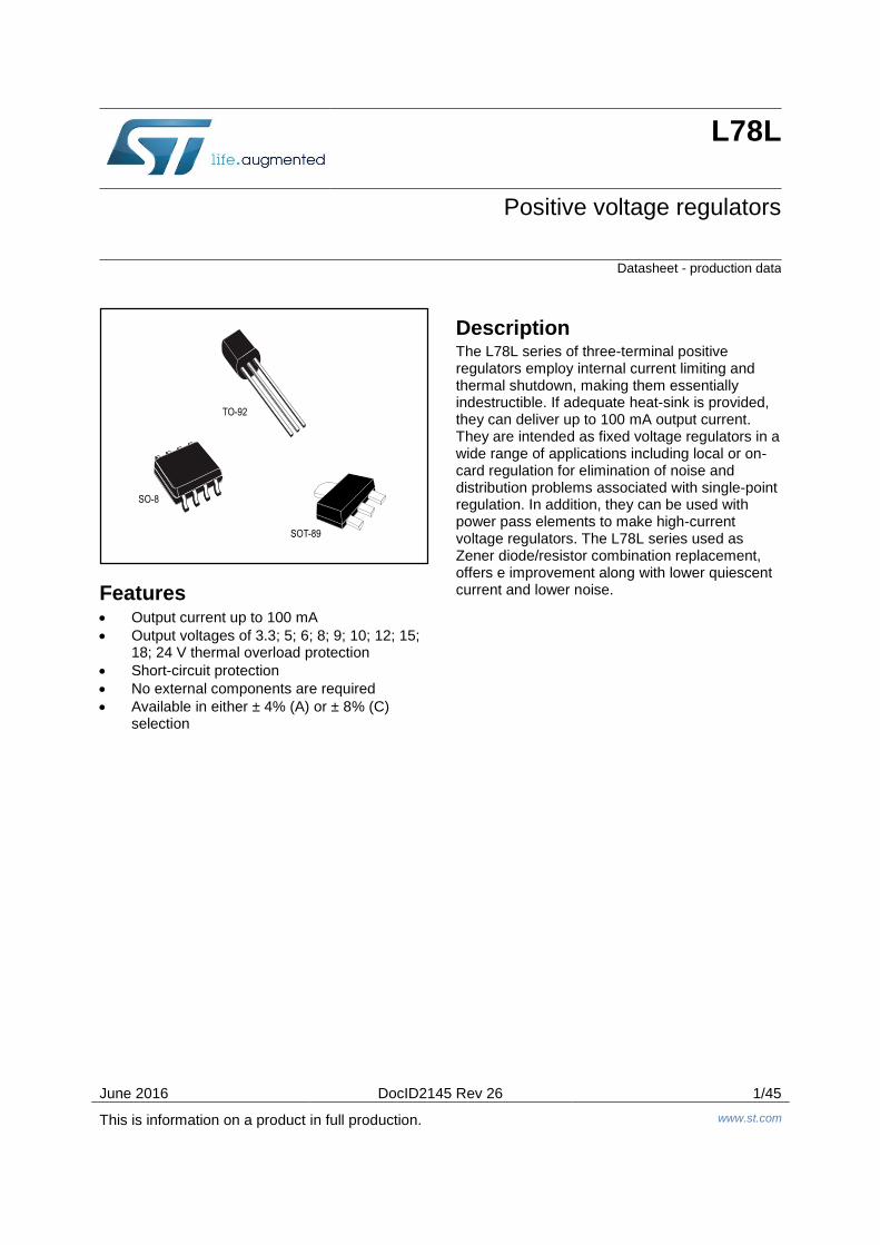
June 2016 DocID2145 Rev 26 1/45
This is information on a product in full production. www.st.com
L78L
Positive voltage regulators
Datasheet - production data
Features Output current up to 100 mA
Output voltages of 3.3; 5; 6; 8; 9; 10; 12; 15; 18; 24 V thermal overload protection
Short-circuit protection
No external components are required
Available in either ± 4% (A) or ± 8% (C) selection
Description The L78L series of three-terminal positive regulators employ internal current limiting and thermal shutdown, making them essentially indestructible. If adequate heat-sink is provided, they can deliver up to 100 mA output current. They are intended as fixed voltage regulators in a wide range of applications including local or on-card regulation for elimination of noise and distribution problems associated with single-point regulation. In addition, they can be used with power pass elements to make high-current voltage regulators. The L78L series used as Zener diode/resistor combination replacement, offers e improvement along with lower quiescent current and lower noise.
Contents L78L
2/45 DocID2145 Rev 26
Contents
1 Diagram ............................................................................................ 3
2 Pin configuration ............................................................................. 4
3 Maximum ratings ............................................................................. 5
4 Electrical characteristics ................................................................ 6
5 Typical performance ..................................................................... 25
6 Typical application ........................................................................ 27
7 Package information ..................................................................... 29
7.1 TO-92 package information ............................................................. 29
7.2 TO-92 packing information .............................................................. 30
7.3 TO-92 Ammopak packing information ............................................. 32
7.4 SO-8 package information .............................................................. 34
7.5 SO-8 packing information ................................................................ 36
7.6 SOT-89 package information .......................................................... 37
7.7 SOT-89 packing information............................................................ 40
8 Ordering information ..................................................................... 41
9 Revision history ............................................................................ 44
L78L Diagram
DocID2145 Rev 26 3/45
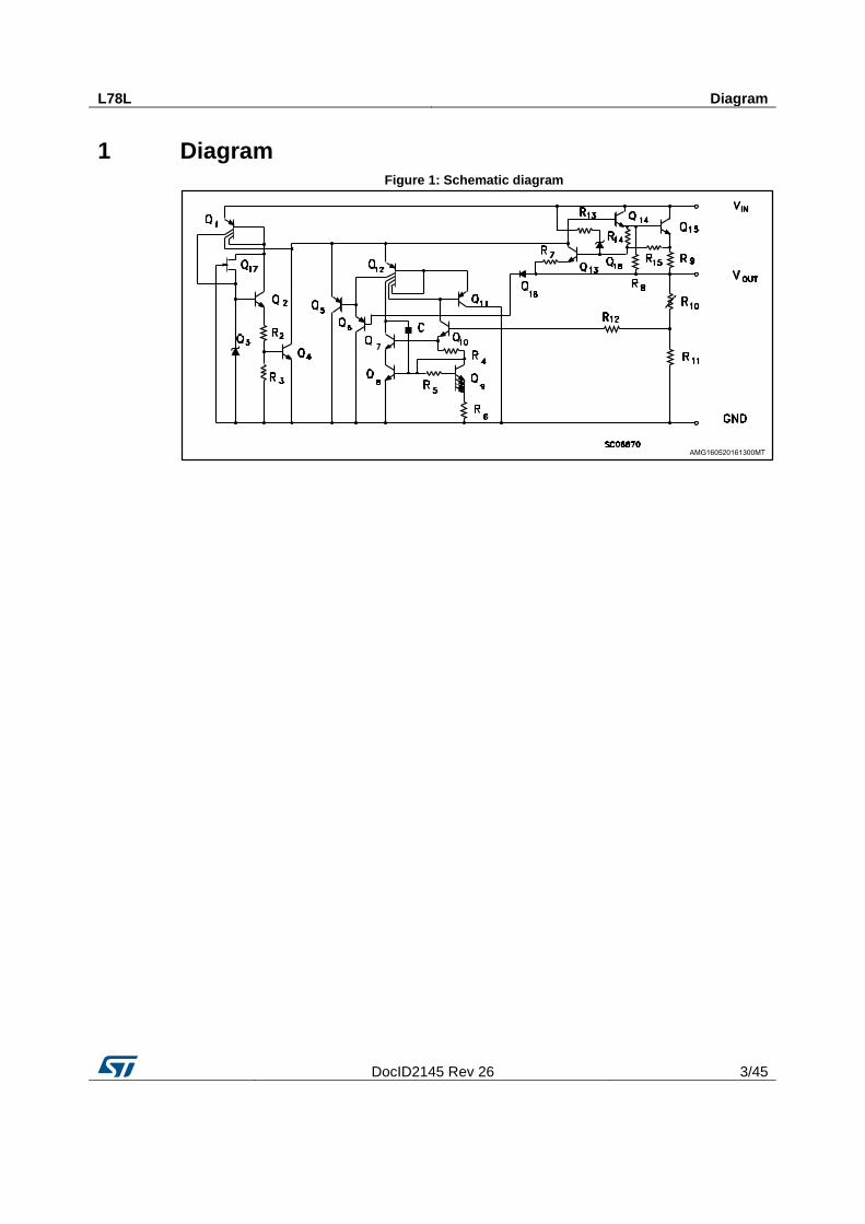
1 Diagram Figure 1: Schematic diagram
Pin configuration L78L
4/45 DocID2145 Rev 26
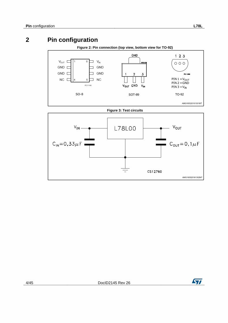
2 Pin configuration Figure 2: Pin connection (top view, bottom view for TO-92)
Figure 3: Test circuits
L78L Maximum ratings
DocID2145 Rev 26 5/45
3 Maximum ratings Table 1: Absolute maximum ratings
Symbol Parameter Value Unit
VI DC Input voltage
VO = 3.3 to 9 V 30
V VO = 12 to 15 V 35
VO = 18 to 24 V 40
IO Output current 100 mA
PD Power dissipation Internally limited (1) mW
TSTG Storage temperature range -65 to 150 °C
TOP Operating junction temperature range for L78LxxAC / L78LxxC 0 to 125
°C for L78LxxAB -40 to 125
Notes:
(1)Our SO-8 package used for voltage regulators is modified internally to have pins 2, 3, 6 and 7 electrically communed to the die attach flag. This particular frame decreases the total thermal resistance of the package and increases its ability to dissipate power when an appropriate area of copper on the printed circuit board is available for heat-sinking. The external dimensions are the same as for the standard SO-8.
Table 2: Thermal data
Symbol Parameter SO-8 TO-92 SOT-89 Unit
RthJC Thermal resistance junction-case (max) 20
15 °C/W
RthJA Thermal resistance junction-ambient (max) 55 (1) 200 55 (1) °C/W
Notes:
(1)Considering 6 cm² of copper Board heat-sink.
Electrical characteristics L78L
6/45 DocID2145 Rev 26
4 Electrical characteristics
Refer to the test circuits, TJ = 0 to 125 °C, VI = 8.3 V, IO = 40 mA, CI = 0.33 µF, CO = 0.1 µF unless otherwise specified.
Table 3: Electrical characteristics of L78L33C
Symbol Parameter Test conditions Min. Typ. Max. Unit
VO Output voltage TJ = 25 °C 3.036 3.3 3.564 V
VO Output voltage IO = 1 to 40 mA, VI = 5.3 to 20 V 2.97
3.63
V IO = 1 to 70 mA, VI = 8.3 V 2.97
3.63
∆VO Line regulation VI = 5.4 to 20 V, TJ = 25 °C
150
mV VI = 6.3 to 20 V, TJ = 25 °C
100
∆VO Load regulation IO = 1 to 100 mA, TJ = 25 °C
60
mV IO = 1 to 40 mA, TJ = 25 °C
30
Id Quiescent current TJ = 25 °C
6 mA
TJ = 125 °C
5.5 mA
∆Id Quiescent current change IO = 1 to 40 mA
0.2
mA VI = 6.3 to 20 V
1.5
eN Output noise voltage B = 10 Hz to 100 kHz, TJ = 25 °C
40
µV
SVR Supply voltage rejection VI = 6.3 to 16.3 V, f = 120 Hz
IO = 40 mA, TJ = 25 °C 41 49
dB
Vd Dropout voltage
2
V
L78L Electrical characteristics
DocID2145 Rev 26 7/45
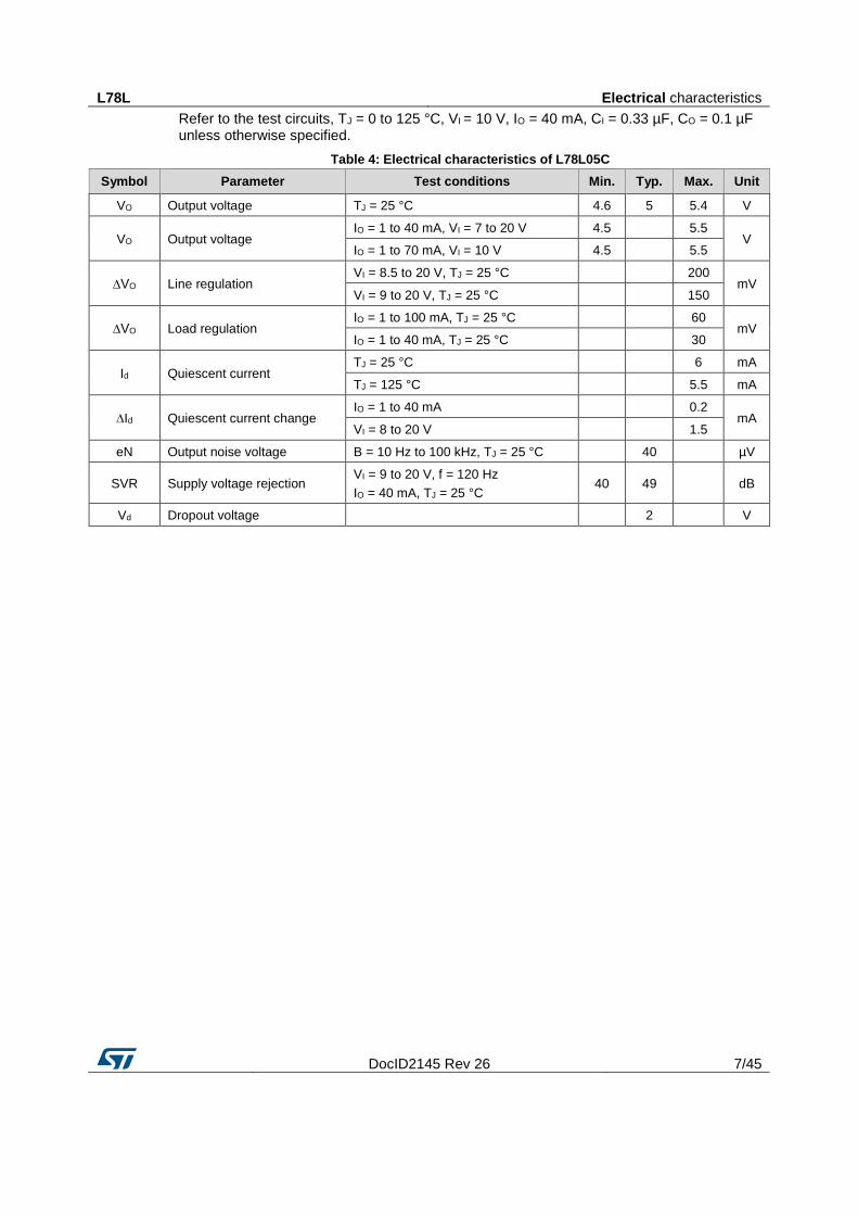
Refer to the test circuits, TJ = 0 to 125 °C, VI = 10 V, IO = 40 mA, CI = 0.33 µF, CO = 0.1 µF unless otherwise specified.
Table 4: Electrical characteristics of L78L05C
Symbol Parameter Test conditions Min. Typ. Max. Unit
VO Output voltage TJ = 25 °C 4.6 5 5.4 V
VO Output voltage IO = 1 to 40 mA, VI = 7 to 20 V 4.5
5.5
V IO = 1 to 70 mA, VI = 10 V 4.5
5.5
∆VO Line regulation VI = 8.5 to 20 V, TJ = 25 °C
200
mV VI = 9 to 20 V, TJ = 25 °C
150
∆VO Load regulation IO = 1 to 100 mA, TJ = 25 °C
60
mV IO = 1 to 40 mA, TJ = 25 °C
30
Id Quiescent current TJ = 25 °C
6 mA
TJ = 125 °C
5.5 mA
∆Id Quiescent current change IO = 1 to 40 mA
0.2
mA VI = 8 to 20 V
1.5
eN Output noise voltage B = 10 Hz to 100 kHz, TJ = 25 °C
40
µV
SVR Supply voltage rejection VI = 9 to 20 V, f = 120 Hz
IO = 40 mA, TJ = 25 °C 40 49
dB
Vd Dropout voltage
2
V

Electrical characteristics L78L
8/45 DocID2145 Rev 26
Refer to the test circuits, TJ = 0 to 125 °C,VI = 14 V, IO = 40 mA, CI = 0.33 µF, CO = 0.1 µF unless otherwise specified.
Table 5: Electrical characteristics of L78L08C
Symbol Parameter Test conditions Min. Typ. Max. Unit
VO Output voltage TJ = 25 °C 7.36 8 8.64 V
VO Output voltage IO = 1 to 40 mA, VI = 8.5 to 20 V 7.2
8.8
V IO = 1 to 70 mA, VI = 12 V 7.2
8.8
∆VO Line regulation VI = 10.5 to 20 V, TJ = 25 °C
200
mV VI = 11 to 20 V, TJ = 25 °C
150
∆VO Load regulation IO = 1 to 100 mA, TJ = 25 °C
80
mV IO = 1 to 40 mA, TJ = 25 °C
40
Id Quiescent current TJ = 25 °C
6 mA
TJ = 125 °C
5.5 mA
∆Id Quiescent current change IO = 1 to 40 mA
0.2
mA VI = 8 to 20 V
1.5
eN Output noise voltage B = 10 Hz to 100 kHz, TJ = 25 °C
60
µV
SVR Supply voltage rejection VI = 9 to 20 V, f = 120 Hz
IO = 40 mA, TJ = 25 °C 36 45
dB
Vd Dropout voltage
1.7
V
L78L Electrical characteristics
DocID2145 Rev 26 9/45
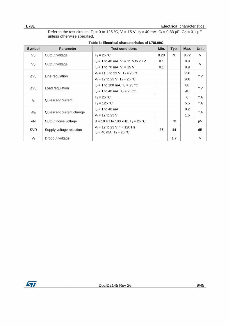
Refer to the test circuits, TJ = 0 to 125 °C, VI = 15 V, IO = 40 mA, CI = 0.33 µF, CO = 0.1 µF unless otherwise specified.
Table 6: Electrical characteristics of L78L09C
Symbol Parameter Test conditions Min. Typ. Max. Unit
VO Output voltage TJ = 25 °C 8.28 9 9.72 V
VO Output voltage IO = 1 to 40 mA, VI = 11.5 to 23 V 8.1
9.9
V IO = 1 to 70 mA, VI = 15 V 8.1
9.9
∆VO Line regulation VI = 11.5 to 23 V, TJ = 25 °C
250
mV VI = 12 to 23 V, TJ = 25 °C
200
∆VO Load regulation IO = 1 to 100 mA, TJ = 25 °C
80
mV IO = 1 to 40 mA, TJ = 25 °C
40
Id Quiescent current TJ = 25 °C
6 mA
TJ = 125 °C
5.5 mA
∆Id Quiescent current change IO = 1 to 40 mA
0.2
mA VI = 12 to 23 V
1.5
eN Output noise voltage B = 10 Hz to 100 kHz, TJ = 25 °C
70
µV
SVR Supply voltage rejection VI = 12 to 23 V, f = 120 Hz
IO = 40 mA, TJ = 25 °C 36 44
dB
Vd Dropout voltage
1.7
V
Electrical characteristics L78L
10/45 DocID2145 Rev 26
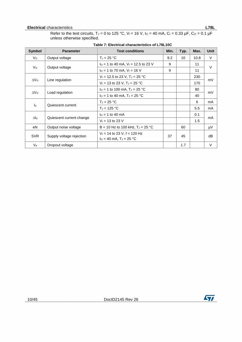
Refer to the test circuits, TJ = 0 to 125 °C, VI = 16 V, IO = 40 mA, CI = 0.33 µF, CO = 0.1 µF unless otherwise specified.
Table 7: Electrical characteristics of L78L10C
Symbol Parameter Test conditions Min. Typ. Max. Unit
VO Output voltage TJ = 25 °C 9.2 10 10.8 V
VO Output voltage IO = 1 to 40 mA, VI = 12.5 to 23 V 9
11
V IO = 1 to 70 mA, VI = 16 V 9
11
∆VO Line regulation VI = 12.5 to 23 V, TJ = 25 °C
230
mV VI = 13 to 23 V, TJ = 25 °C
170
∆VO Load regulation IO = 1 to 100 mA, TJ = 25 °C
80
mV IO = 1 to 40 mA, TJ = 25 °C
40
Id Quiescent current TJ = 25 °C
6 mA
TJ = 125 °C
5.5 mA
∆Id Quiescent current change IO = 1 to 40 mA
0.1
mA VI = 13 to 23 V
1.5
eN Output noise voltage B = 10 Hz to 100 kHz, TJ = 25 °C
60
µV
SVR Supply voltage rejection VI = 14 to 23 V, f = 120 Hz
IO = 40 mA, TJ = 25 °C 37 45
dB
Vd Dropout voltage
1.7
V
L78L Electrical characteristics
DocID2145 Rev 26 11/45
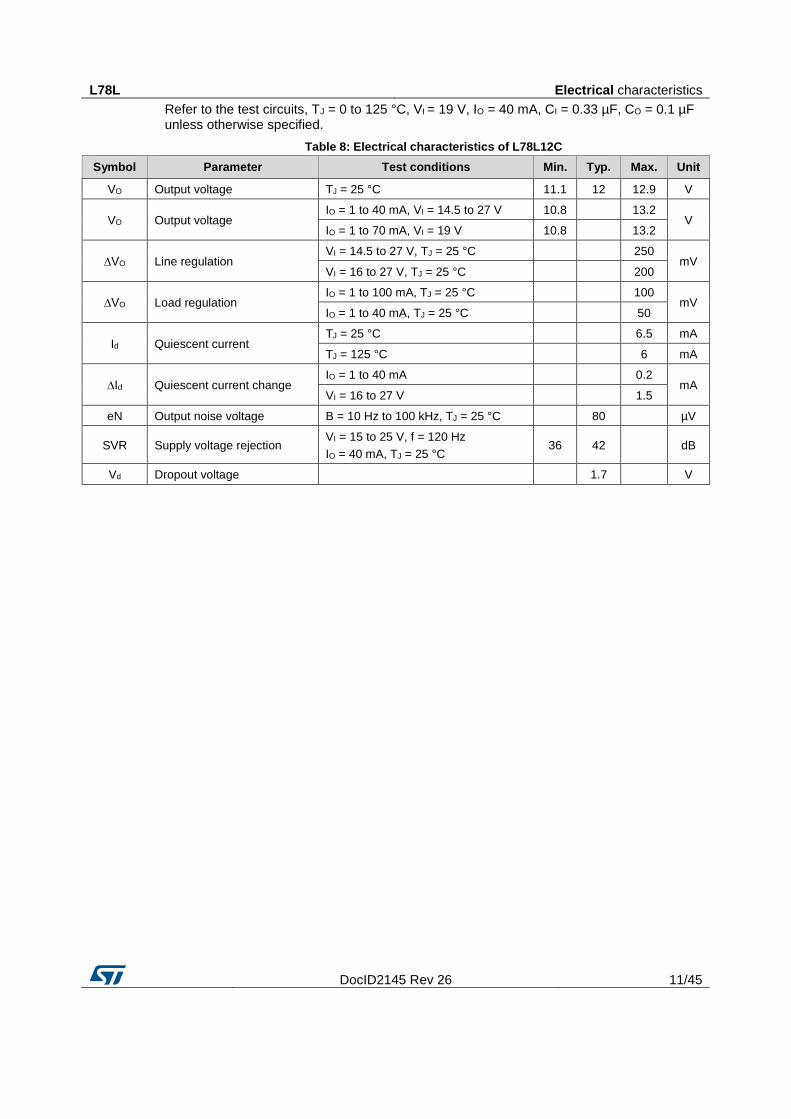
Refer to the test circuits, TJ = 0 to 125 °C, VI = 19 V, IO = 40 mA, CI = 0.33 µF, CO = 0.1 µF unless otherwise specified.
Table 8: Electrical characteristics of L78L12C
Symbol Parameter Test conditions Min. Typ. Max. Unit
VO Output voltage TJ = 25 °C 11.1 12 12.9 V
VO Output voltage IO = 1 to 40 mA, VI = 14.5 to 27 V 10.8
13.2
V IO = 1 to 70 mA, VI = 19 V 10.8
13.2
∆VO Line regulation VI = 14.5 to 27 V, TJ = 25 °C
250
mV VI = 16 to 27 V, TJ = 25 °C
200
∆VO Load regulation IO = 1 to 100 mA, TJ = 25 °C
100
mV IO = 1 to 40 mA, TJ = 25 °C
50
Id Quiescent current TJ = 25 °C
6.5 mA
TJ = 125 °C
6 mA
∆Id Quiescent current change IO = 1 to 40 mA
0.2
mA VI = 16 to 27 V
1.5
eN Output noise voltage B = 10 Hz to 100 kHz, TJ = 25 °C
80
µV
SVR Supply voltage rejection VI = 15 to 25 V, f = 120 Hz
IO = 40 mA, TJ = 25 °C 36 42
dB
Vd Dropout voltage
1.7
V

Electrical characteristics L78L
12/45 DocID2145 Rev 26
Refer to the test circuits, TJ = 0 to 125 °C, VI = 23 V, IO = 40 mA, CI = 0.33 µF, CO = 0.1 µF unless otherwise specified
Table 9: Electrical characteristics of L78L15C
Symbol Parameter Test conditions Min. Typ. Max. Unit
VO Output voltage TJ = 25 °C 13.8 15 16.2 V
VO Output voltage IO = 1 to 40 mA, VI = 17.5 to 30 V 13.5
16.5
V IO = 1 to 70 mA, VI = 23 V 13.5
16.5
∆VO Line regulation VI = 17.5 to 30 V, TJ = 25 °C
300
mV VI = 20 to 30 V, TJ = 25 °C
250
∆VO Load regulation IO = 1 to 100 mA, TJ = 25 °C
150
mV IO = 1 to 40 mA, TJ = 25 °C
75
Id Quiescent current TJ = 25 °C
6.5 mA
TJ = 125 °C
6 mA
∆Id Quiescent current change IO = 1 to 40 mA
0.2
mA VI = 20 to 30 V
1.5
eN Output noise voltage B = 10 Hz to 100 kHz, TJ = 25 °C
90
µV
SVR Supply voltage rejection VI = 18.5 to 28.5 V, f = 120 Hz
IO = 40 mA, TJ = 25 °C 33 39
dB
Vd Dropout voltage
1.7
V
L78L Electrical characteristics
DocID2145 Rev 26 13/45
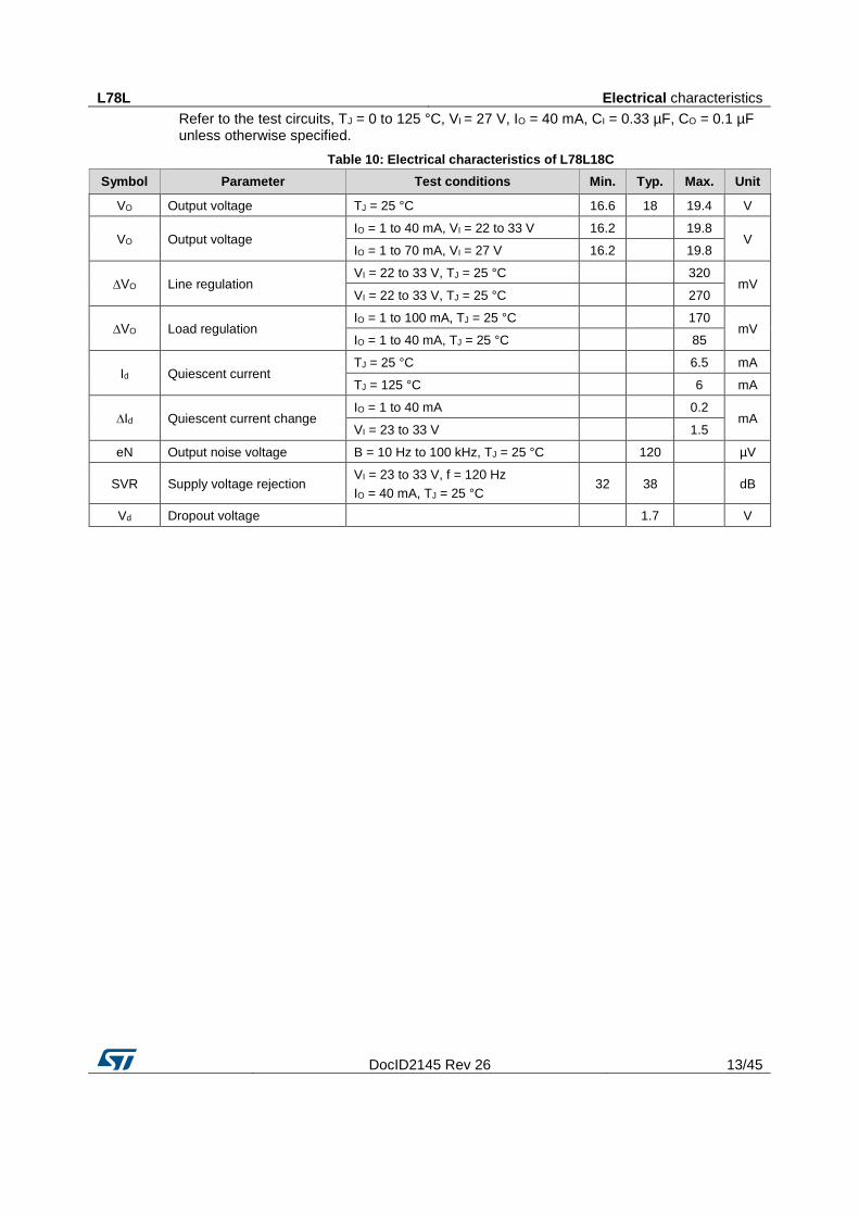
Refer to the test circuits, TJ = 0 to 125 °C, VI = 27 V, IO = 40 mA, CI = 0.33 µF, CO = 0.1 µF unless otherwise specified.
Table 10: Electrical characteristics of L78L18C
Symbol Parameter Test conditions Min. Typ. Max. Unit
VO Output voltage TJ = 25 °C 16.6 18 19.4 V
VO Output voltage IO = 1 to 40 mA, VI = 22 to 33 V 16.2
19.8
V IO = 1 to 70 mA, VI = 27 V 16.2
19.8
∆VO Line regulation VI = 22 to 33 V, TJ = 25 °C
320
mV VI = 22 to 33 V, TJ = 25 °C
270
∆VO Load regulation IO = 1 to 100 mA, TJ = 25 °C
170
mV IO = 1 to 40 mA, TJ = 25 °C
85
Id Quiescent current TJ = 25 °C
6.5 mA
TJ = 125 °C
6 mA
∆Id Quiescent current change IO = 1 to 40 mA
0.2
mA VI = 23 to 33 V
1.5
eN Output noise voltage B = 10 Hz to 100 kHz, TJ = 25 °C
120
µV
SVR Supply voltage rejection VI = 23 to 33 V, f = 120 Hz
IO = 40 mA, TJ = 25 °C 32 38
dB
Vd Dropout voltage
1.7
V
Electrical characteristics L78L
14/45 DocID2145 Rev 26
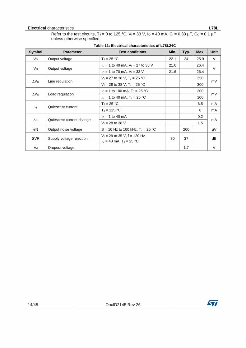
Refer to the test circuits, TJ = 0 to 125 °C, VI = 33 V, IO = 40 mA, CI = 0.33 µF, CO = 0.1 µF unless otherwise specified.
Table 11: Electrical characteristics of L78L24C
Symbol Parameter Test conditions Min. Typ. Max. Unit
VO Output voltage TJ = 25 °C 22.1 24 25.9 V
VO Output voltage IO = 1 to 40 mA, VI = 27 to 38 V 21.6
26.4
V IO = 1 to 70 mA, VI = 33 V 21.6
26.4
∆VO Line regulation VI = 27 to 38 V, TJ = 25 °C
350
mV VI = 28 to 38 V, TJ = 25 °C
300
∆VO Load regulation IO = 1 to 100 mA, TJ = 25 °C
200
mV IO = 1 to 40 mA, TJ = 25 °C
100
Id Quiescent current TJ = 25 °C
6.5 mA
TJ = 125 °C
6 mA
∆Id Quiescent current change IO = 1 to 40 mA
0.2
mA VI = 28 to 38 V
1.5
eN Output noise voltage B = 10 Hz to 100 kHz, TJ = 25 °C
200
µV
SVR Supply voltage rejection VI = 29 to 35 V, f = 120 Hz
IO = 40 mA, TJ = 25 °C 30 37
dB
Vd Dropout voltage
1.7
V
L78L Electrical characteristics
DocID2145 Rev 26 15/45
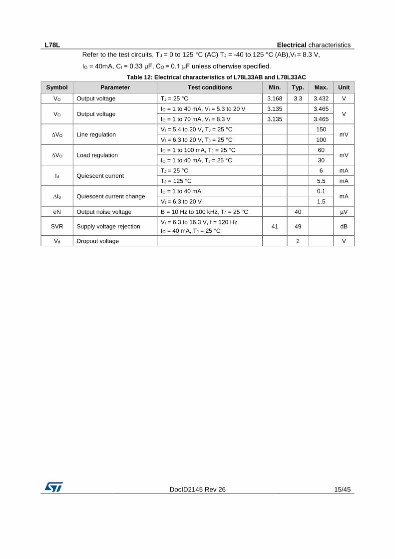
Refer to the test circuits, TJ = 0 to 125 °C (AC) TJ = -40 to 125 °C (AB),VI = 8.3 V,
IO = 40mA, CI = 0.33 μF, CO = 0.1 μF unless otherwise specified.
Table 12: Electrical characteristics of L78L33AB and L78L33AC
Symbol Parameter Test conditions Min. Typ. Max. Unit
VO Output voltage TJ = 25 °C 3.168 3.3 3.432 V
VO Output voltage IO = 1 to 40 mA, VI = 5.3 to 20 V 3.135
3.465
V IO = 1 to 70 mA, VI = 8.3 V 3.135
3.465
∆VO Line regulation VI = 5.4 to 20 V, TJ = 25 °C
150
mV VI = 6.3 to 20 V, TJ = 25 °C
100
∆VO Load regulation IO = 1 to 100 mA, TJ = 25 °C
60
mV IO = 1 to 40 mA, TJ = 25 °C
30
Id Quiescent current TJ = 25 °C
6 mA
TJ = 125 °C
5.5 mA
∆Id Quiescent current change IO = 1 to 40 mA
0.1
mA VI = 6.3 to 20 V
1.5
eN Output noise voltage B = 10 Hz to 100 kHz, TJ = 25 °C
40
µV
SVR Supply voltage rejection VI = 6.3 to 16.3 V, f = 120 Hz
IO = 40 mA, TJ = 25 °C 41 49
dB
Vd Dropout voltage
2
V
Electrical characteristics L78L
16/45 DocID2145 Rev 26
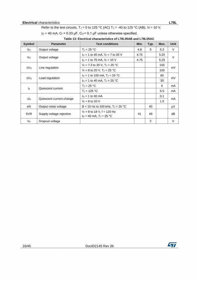
Refer to the test circuits, TJ = 0 to 125 °C (AC) TJ = -40 to 125 °C (AB), VI = 10 V,
IO = 40 mA, CI = 0.33 μF, CO = 0.1 μF unless otherwise specified.
Table 13: Electrical characteristics of L78L05AB and L78L05AC
Symbol Parameter Test conditions Min. Typ. Max. Unit
VO Output voltage TJ = 25 °C 4.8 5 5.2 V
VO Output voltage IO = 1 to 40 mA, VI = 7 to 20 V 4.75
5.25
V IO = 1 to 70 mA, VI = 10 V 4.75
5.25
∆VO Line regulation VI = 7.3 to 20 V, TJ = 25 °C
150
mV VI = 8 to 20 V, TJ = 25 °C
100
∆VO Load regulation IO = 1 to 100 mA, TJ = 25 °C
60
mV IO = 1 to 40 mA, TJ = 25 °C
30
Id Quiescent current TJ = 25 °C
6 mA
TJ = 125 °C
5.5 mA
∆Id Quiescent current change IO = 1 to 40 mA
0.1
mA VI = 8 to 20 V
1.5
eN Output noise voltage B = 10 Hz to 100 kHz, TJ = 25 °C
40
µV
SVR Supply voltage rejection VI = 8 to 18 V, f = 120 Hz
IO = 40 mA, TJ = 25 °C 41 49
dB
Vd Dropout voltage
2
V
L78L Electrical characteristics
DocID2145 Rev 26 17/45
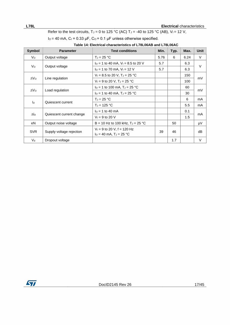
Refer to the test circuits, TJ = 0 to 125 °C (AC) TJ = -40 to 125 °C (AB), VI = 12 V,
IO = 40 mA, CI = 0.33 μF, CO = 0.1 μF unless otherwise specified.
Table 14: Electrical characteristics of L78L06AB and L78L06AC
Symbol Parameter Test conditions Min. Typ. Max. Unit
VO Output voltage TJ = 25 °C 5.76 6 6.24 V
VO Output voltage IO = 1 to 40 mA, VI = 8.5 to 20 V 5.7
6.3
V IO = 1 to 70 mA, VI = 12 V 5.7
6.3
∆VO Line regulation VI = 8.5 to 20 V, TJ = 25 °C
150
mV VI = 9 to 20 V, TJ = 25 °C
100
∆VO Load regulation IO = 1 to 100 mA, TJ = 25 °C
60
mV IO = 1 to 40 mA, TJ = 25 °C
30
Id Quiescent current TJ = 25 °C
6 mA
TJ = 125 °C
5.5 mA
∆Id Quiescent current change IO = 1 to 40 mA
0.1
mA VI = 9 to 20 V
1.5
eN Output noise voltage B = 10 Hz to 100 kHz, TJ = 25 °C
50
µV
SVR Supply voltage rejection VI = 9 to 20 V, f = 120 Hz
IO = 40 mA, TJ = 25 °C 39 46
dB
Vd Dropout voltage
1.7
V
Electrical characteristics L78L
18/45 DocID2145 Rev 26
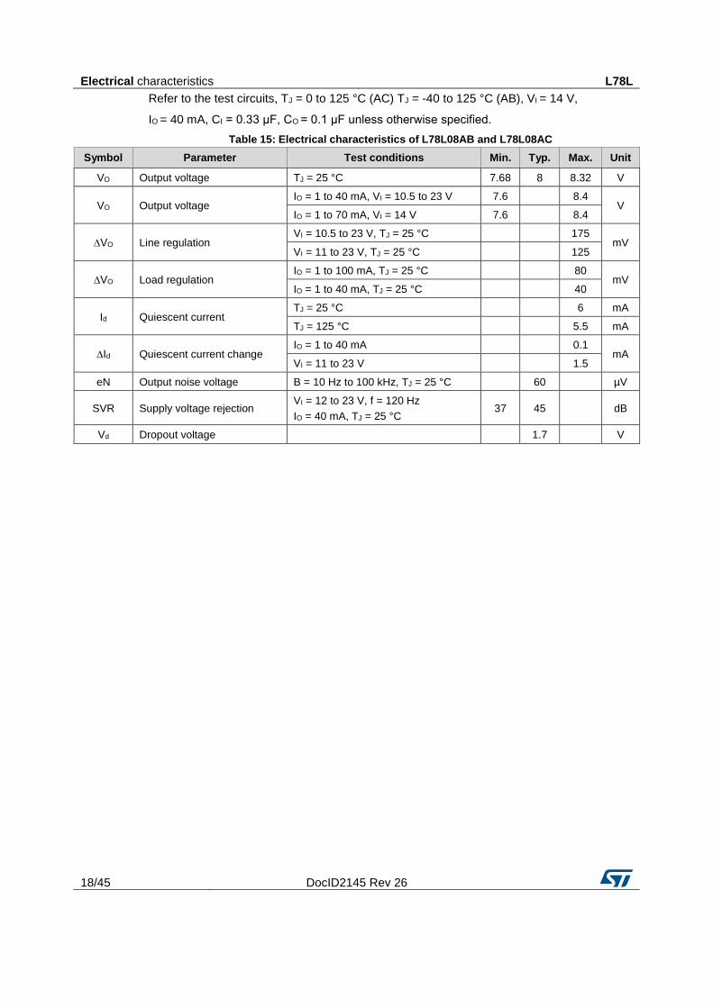
Refer to the test circuits, TJ = 0 to 125 °C (AC) TJ = -40 to 125 °C (AB), VI = 14 V,
IO = 40 mA, CI = 0.33 μF, CO = 0.1 μF unless otherwise specified.
Table 15: Electrical characteristics of L78L08AB and L78L08AC
Symbol Parameter Test conditions Min. Typ. Max. Unit
VO Output voltage TJ = 25 °C 7.68 8 8.32 V
VO Output voltage IO = 1 to 40 mA, VI = 10.5 to 23 V 7.6
8.4
V IO = 1 to 70 mA, VI = 14 V 7.6
8.4
∆VO Line regulation VI = 10.5 to 23 V, TJ = 25 °C
175
mV VI = 11 to 23 V, TJ = 25 °C
125
∆VO Load regulation IO = 1 to 100 mA, TJ = 25 °C
80
mV IO = 1 to 40 mA, TJ = 25 °C
40
Id Quiescent current TJ = 25 °C
6 mA
TJ = 125 °C
5.5 mA
∆Id Quiescent current change IO = 1 to 40 mA
0.1
mA VI = 11 to 23 V
1.5
eN Output noise voltage B = 10 Hz to 100 kHz, TJ = 25 °C
60
µV
SVR Supply voltage rejection VI = 12 to 23 V, f = 120 Hz
IO = 40 mA, TJ = 25 °C 37 45
dB
Vd Dropout voltage
1.7
V
L78L Electrical characteristics
DocID2145 Rev 26 19/45
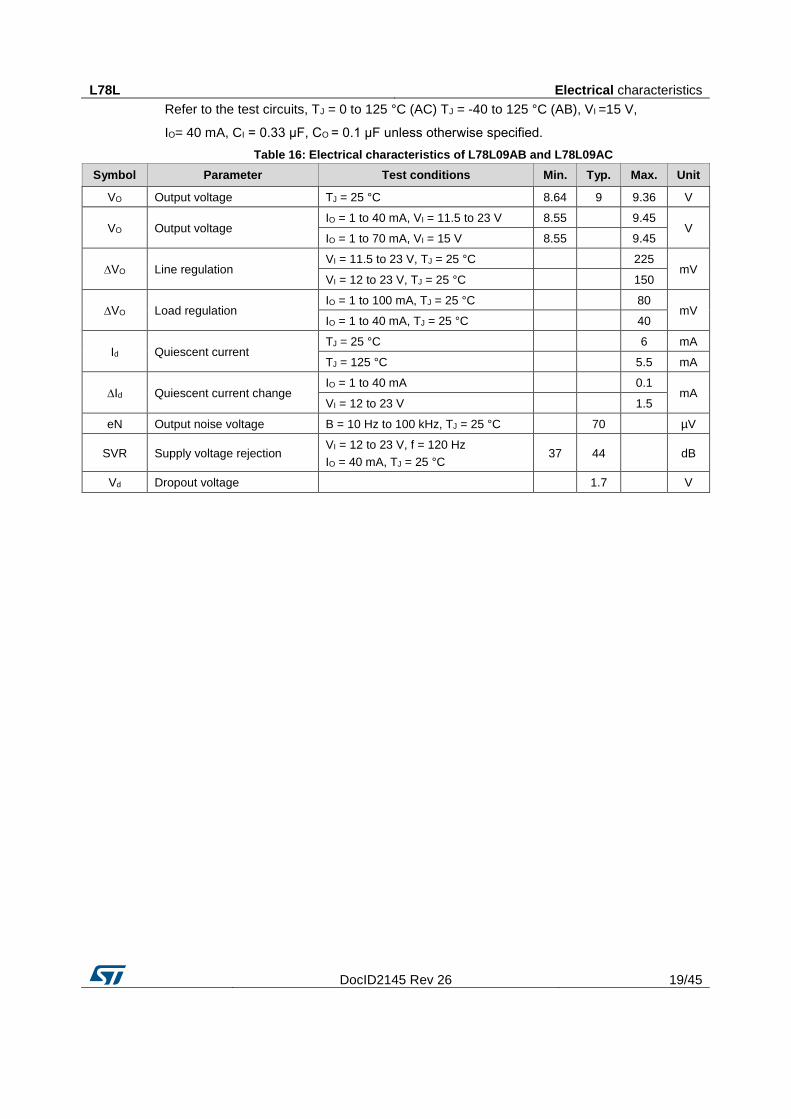
Refer to the test circuits, TJ = 0 to 125 °C (AC) TJ = -40 to 125 °C (AB), VI =15 V,
IO= 40 mA, CI = 0.33 μF, CO = 0.1 μF unless otherwise specified.
Table 16: Electrical characteristics of L78L09AB and L78L09AC
Symbol Parameter Test conditions Min. Typ. Max. Unit
VO Output voltage TJ = 25 °C 8.64 9 9.36 V
VO Output voltage IO = 1 to 40 mA, VI = 11.5 to 23 V 8.55
9.45
V IO = 1 to 70 mA, VI = 15 V 8.55
9.45
∆VO Line regulation VI = 11.5 to 23 V, TJ = 25 °C
225
mV VI = 12 to 23 V, TJ = 25 °C
150
∆VO Load regulation IO = 1 to 100 mA, TJ = 25 °C
80
mV IO = 1 to 40 mA, TJ = 25 °C
40
Id Quiescent current TJ = 25 °C
6 mA
TJ = 125 °C
5.5 mA
∆Id Quiescent current change IO = 1 to 40 mA
0.1
mA VI = 12 to 23 V
1.5
eN Output noise voltage B = 10 Hz to 100 kHz, TJ = 25 °C
70
µV
SVR Supply voltage rejection VI = 12 to 23 V, f = 120 Hz
IO = 40 mA, TJ = 25 °C 37 44
dB
Vd Dropout voltage
1.7
V
Electrical characteristics L78L
20/45 DocID2145 Rev 26
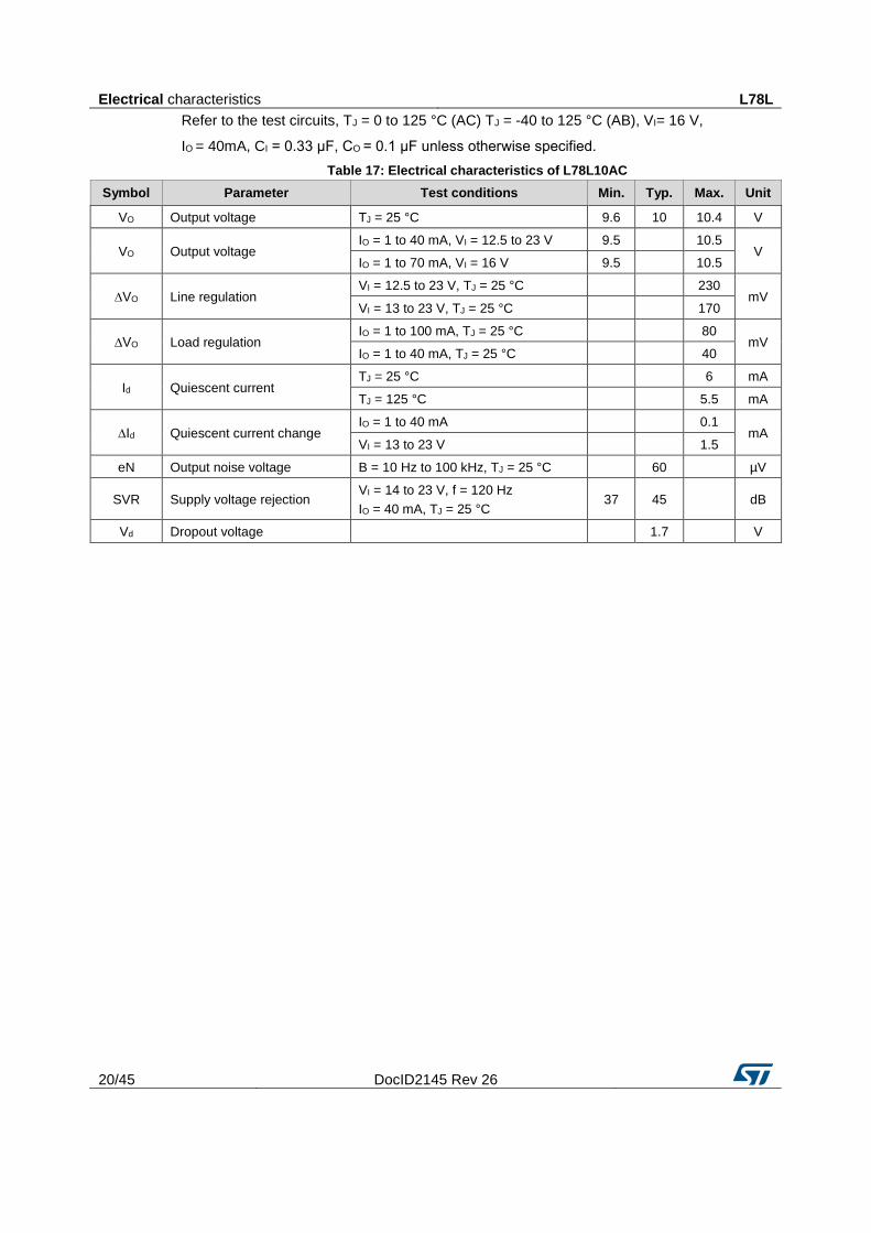
Refer to the test circuits, TJ = 0 to 125 °C (AC) TJ = -40 to 125 °C (AB), VI= 16 V,
IO = 40mA, CI = 0.33 μF, CO = 0.1 μF unless otherwise specified.
Table 17: Electrical characteristics of L78L10AC
Symbol Parameter Test conditions Min. Typ. Max. Unit
VO Output voltage TJ = 25 °C 9.6 10 10.4 V
VO Output voltage IO = 1 to 40 mA, VI = 12.5 to 23 V 9.5
10.5
V IO = 1 to 70 mA, VI = 16 V 9.5
10.5
∆VO Line regulation VI = 12.5 to 23 V, TJ = 25 °C
230
mV VI = 13 to 23 V, TJ = 25 °C
170
∆VO Load regulation IO = 1 to 100 mA, TJ = 25 °C
80
mV IO = 1 to 40 mA, TJ = 25 °C
40
Id Quiescent current TJ = 25 °C
6 mA
TJ = 125 °C
5.5 mA
∆Id Quiescent current change IO = 1 to 40 mA
0.1
mA VI = 13 to 23 V
1.5
eN Output noise voltage B = 10 Hz to 100 kHz, TJ = 25 °C
60
µV
SVR Supply voltage rejection VI = 14 to 23 V, f = 120 Hz
IO = 40 mA, TJ = 25 °C 37 45
dB
Vd Dropout voltage
1.7
V
L78L Electrical characteristics
DocID2145 Rev 26 21/45
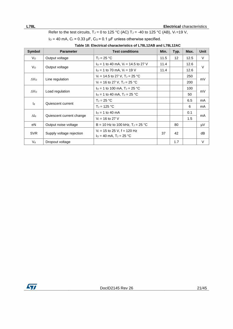
Refer to the test circuits, TJ = 0 to 125 °C (AC) TJ = -40 to 125 °C (AB), VI =19 V,
IO = 40 mA, CI = 0.33 μF, CO = 0.1 μF unless otherwise specified.
Table 18: Electrical characteristics of L78L12AB and L78L12AC
Symbol Parameter Test conditions Min. Typ. Max. Unit
VO Output voltage TJ = 25 °C 11.5 12 12.5 V
VO Output voltage IO = 1 to 40 mA, VI = 14.5 to 27 V 11.4
12.6
V IO = 1 to 70 mA, VI = 19 V 11.4
12.6
∆VO Line regulation VI = 14.5 to 27 V, TJ = 25 °C
250
mV VI = 16 to 27 V, TJ = 25 °C
200
∆VO Load regulation IO = 1 to 100 mA, TJ = 25 °C
100
mV IO = 1 to 40 mA, TJ = 25 °C
50
Id Quiescent current TJ = 25 °C
6.5 mA
TJ = 125 °C
6 mA
∆Id Quiescent current change IO = 1 to 40 mA
0.1
mA VI = 16 to 27 V
1.5
eN Output noise voltage B = 10 Hz to 100 kHz, TJ = 25 °C
80
µV
SVR Supply voltage rejection VI = 15 to 25 V, f = 120 Hz
IO = 40 mA, TJ = 25 °C 37 42
dB
Vd Dropout voltage
1.7
V

Electrical characteristics L78L
22/45 DocID2145 Rev 26
Refer to the test circuits, TJ = 0 to 125 °C (AC) TJ = -40 to 125 °C (AB),VI = 23 V,
IO= 40 mA, CI = 0.33 μF, CO = 0.1 μF unless otherwise specified.
Table 19: Electrical characteristics of L78L15AB and L78L15AC
Symbol Parameter Test conditions Min. Typ. Max. Unit
VO Output voltage TJ = 25 °C 14.4 15 15.6 V
VO Output voltage IO = 1 to 40 mA, VI = 17.5 to 30 V 14.25
15.75
V IO = 1 to 70 mA, VI = 23 V 14.25
15.75
∆VO Line regulation VI = 17.5 to 30 V, TJ = 25 °C
300
mV VI = 20 to 30 V, TJ = 25 °C
250
∆VO Load regulation IO = 1 to 100 mA, TJ = 25 °C
150
mV IO = 1 to 40 mA, TJ = 25 °C
75
Id Quiescent current TJ = 25 °C
6.5 mA
TJ = 125 °C
6 mA
∆Id Quiescent current change IO = 1 to 40 mA
0.1
mA VI = 20 to 30 V
1.5
eN Output noise voltage B = 10 Hz to 100 kHz, TJ = 25 °C
90
µV
SVR Supply voltage rejection VI = 18.5 to 28.5 V, f = 120 Hz
IO = 40 mA, TJ = 25 °C 34 39
dB
Vd Dropout voltage
1.7
V
L78L Electrical characteristics
DocID2145 Rev 26 23/45
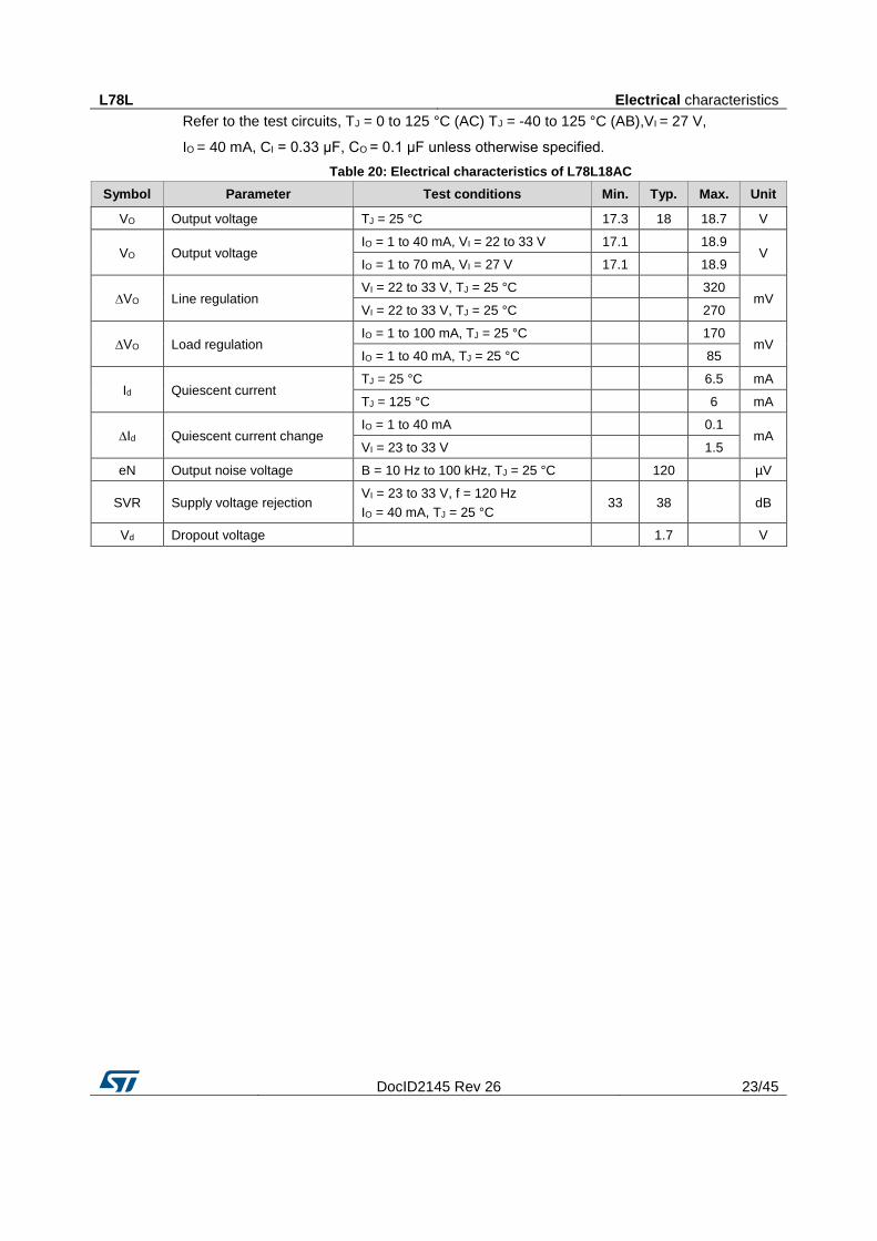
Refer to the test circuits, TJ = 0 to 125 °C (AC) TJ = -40 to 125 °C (AB),VI = 27 V,
IO = 40 mA, CI = 0.33 μF, CO = 0.1 μF unless otherwise specified.
Table 20: Electrical characteristics of L78L18AC
Symbol Parameter Test conditions Min. Typ. Max. Unit
VO Output voltage TJ = 25 °C 17.3 18 18.7 V
VO Output voltage IO = 1 to 40 mA, VI = 22 to 33 V 17.1
18.9
V IO = 1 to 70 mA, VI = 27 V 17.1
18.9
∆VO Line regulation VI = 22 to 33 V, TJ = 25 °C
320
mV VI = 22 to 33 V, TJ = 25 °C
270
∆VO Load regulation IO = 1 to 100 mA, TJ = 25 °C
170
mV IO = 1 to 40 mA, TJ = 25 °C
85
Id Quiescent current TJ = 25 °C
6.5 mA
TJ = 125 °C
6 mA
∆Id Quiescent current change IO = 1 to 40 mA
0.1
mA VI = 23 to 33 V
1.5
eN Output noise voltage B = 10 Hz to 100 kHz, TJ = 25 °C
120
µV
SVR Supply voltage rejection VI = 23 to 33 V, f = 120 Hz
IO = 40 mA, TJ = 25 °C 33 38
dB
Vd Dropout voltage
1.7
V

Electrical characteristics L78L
24/45 DocID2145 Rev 26
Refer to the test circuits, TJ = 0 to 125 °C (AC) TJ = -40 to 125 °C (AB),VI = 33 V,
IO = 40 mA, CI = 0.33 μF, CO = 0.1 μF unless otherwise specified.
Table 21: Electrical characteristics of L78L24AB and L78L24AC
Symbol Parameter Test conditions Min. Typ. Max. Unit
VO Output voltage TJ = 25 °C 23 24 25 V
VO Output voltage IO = 1 to 40 mA, VI = 27 to 38 V 22.8
25.2
V IO = 1 to 70 mA, VI = 33 V 22.8
25.2
∆VO Line regulation VI = 27 to 38 V, TJ = 25 °C
350
mV VI = 28 to 38 V, TJ = 25 °C
300
∆VO Load regulation IO = 1 to 100 mA, TJ = 25 °C
200
mV IO = 1 to 40 mA, TJ = 25 °C
100
Id Quiescent current TJ = 25 °C
6.5 mA
TJ = 125 °C
6 mA
∆Id Quiescent current change IO = 1 to 40 mA
0.1
mA VI = 28 to 38 V
1.5
eN Output noise voltage B = 10 Hz to 100 kHz, TJ = 25 °C
200
µV5y
SVR Supply voltage rejection VI = 29 to 33 V, f = 120 Hz
IO = 40 mA, TJ = 25 °C 31 37
dB
Vd Dropout voltage
1.7
V
L78L Typical performance
DocID2145 Rev 26 25/45
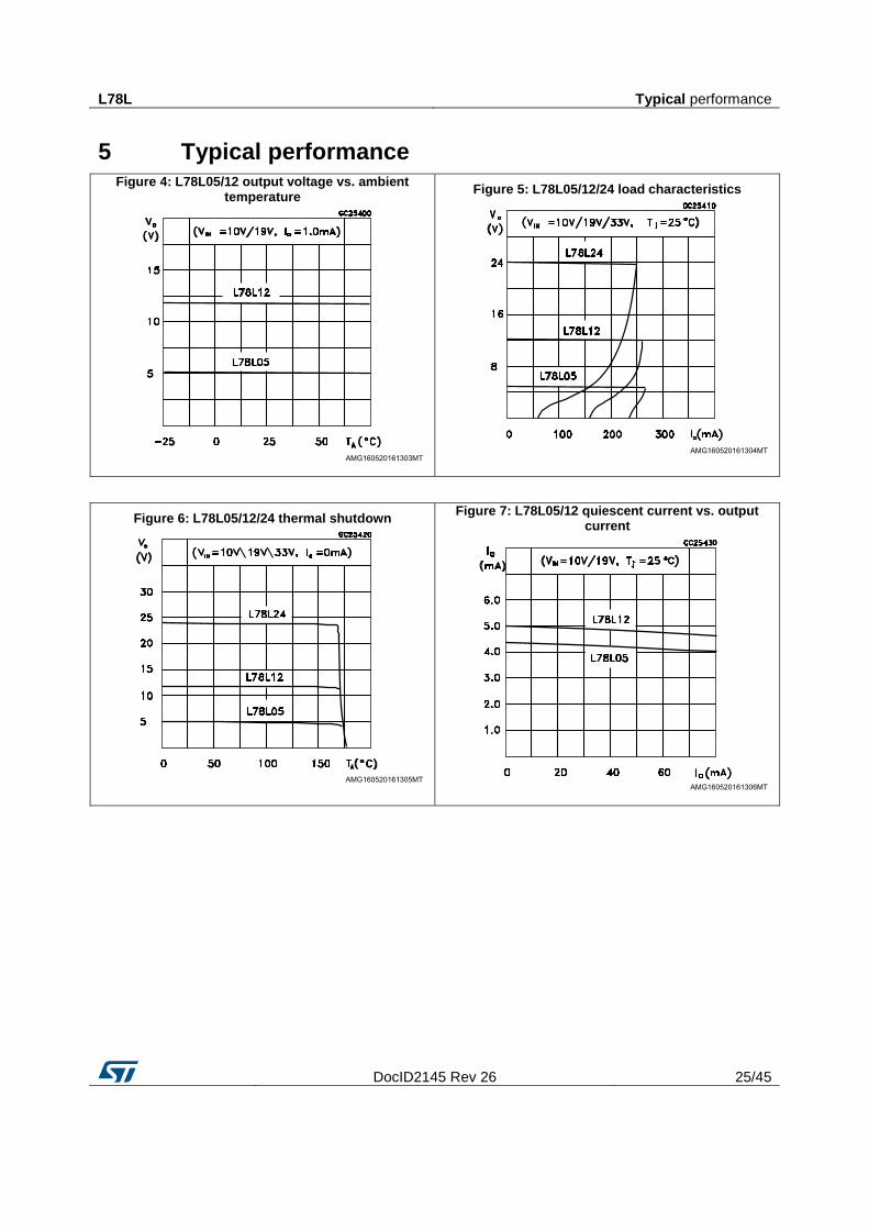
5 Typical performance Figure 4: L78L05/12 output voltage vs. ambient
temperature
Figure 5: L78L05/12/24 load characteristics
Figure 6: L78L05/12/24 thermal shutdown
Figure 7: L78L05/12 quiescent current vs. output current
Typical performance L78L
26/45 DocID2145 Rev 26
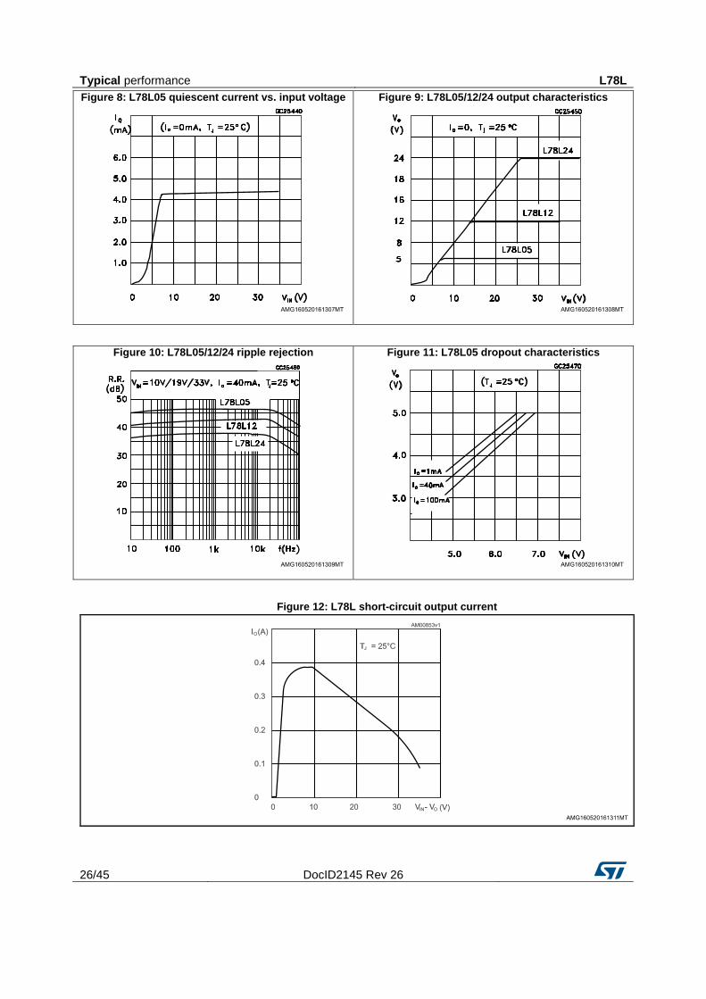
Figure 8: L78L05 quiescent current vs. input voltage
Figure 9: L78L05/12/24 output characteristics
Figure 10: L78L05/12/24 ripple rejection
Figure 11: L78L05 dropout characteristics
Figure 12: L78L short-circuit output current
L78L Typical application
DocID2145 Rev 26 27/45
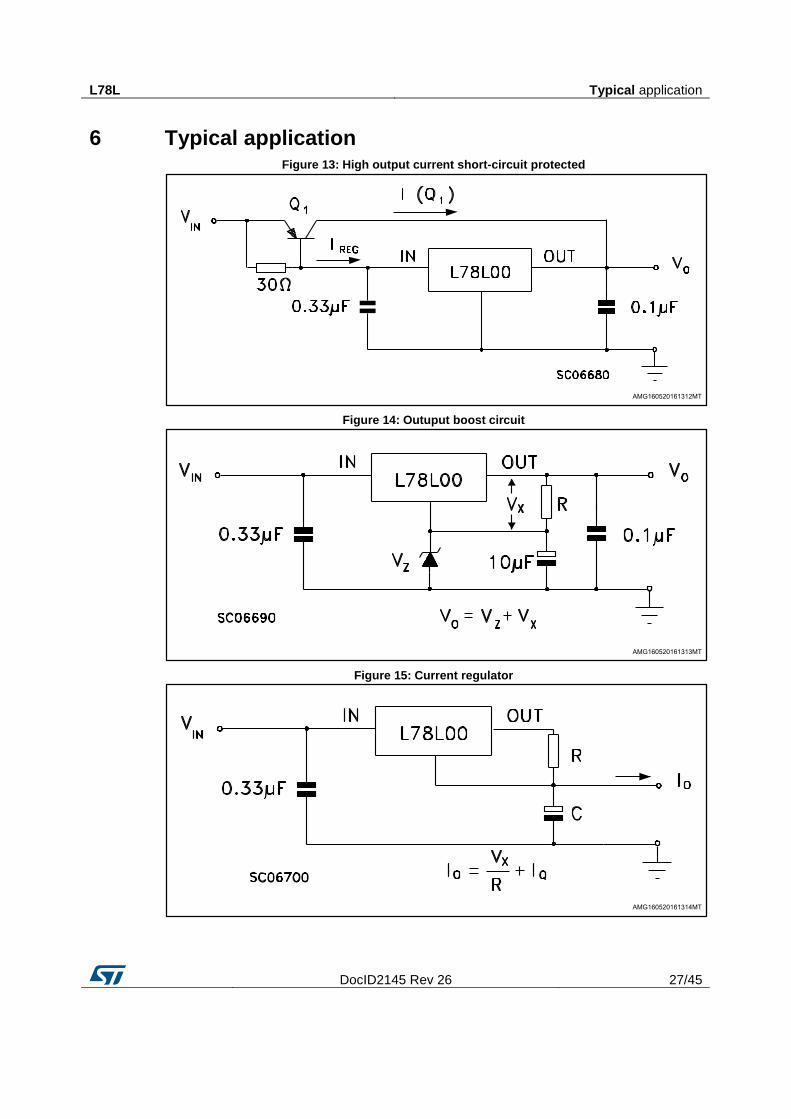
6 Typical application Figure 13: High output current short-circuit protected
Figure 14: Outuput boost circuit
Figure 15: Current regulator
Typical application L78L
28/45 DocID2145 Rev 26
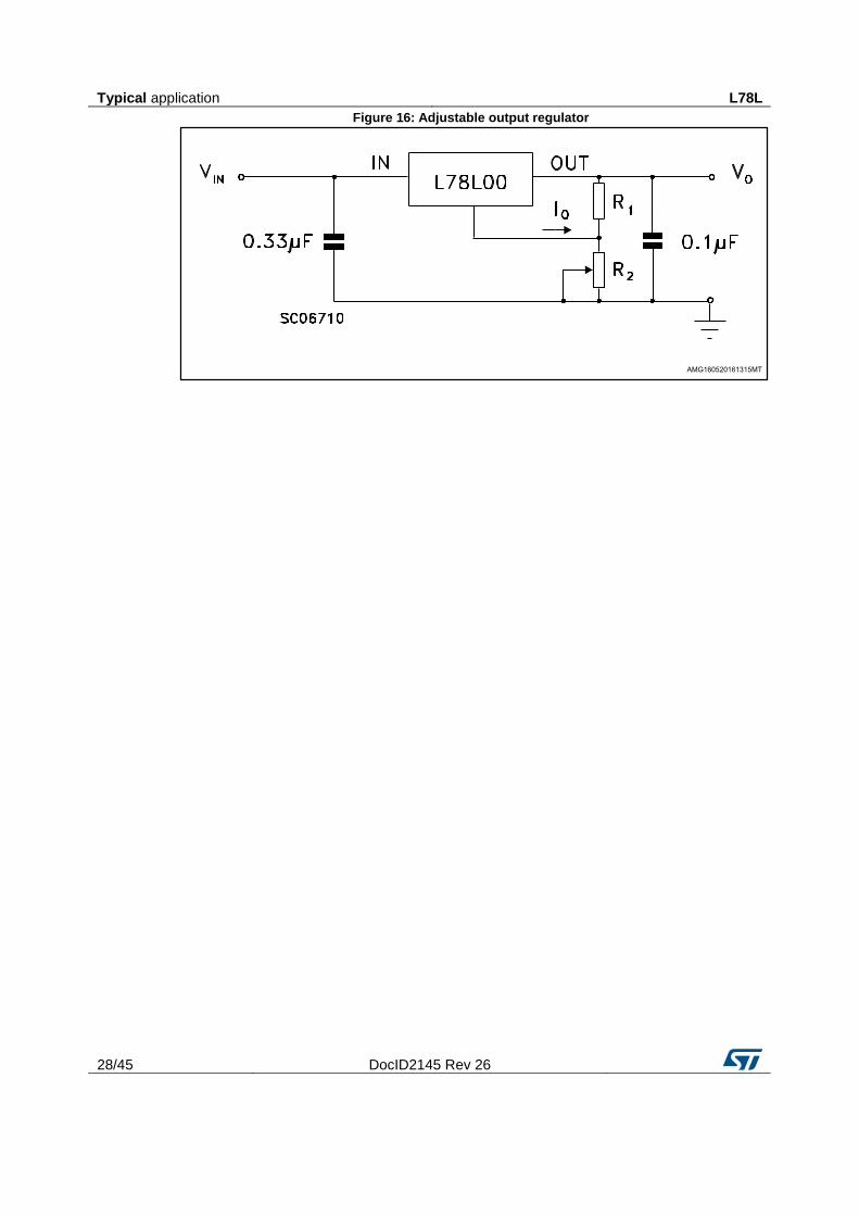
Figure 16: Adjustable output regulator
L78L Package information
DocID2145 Rev 26 29/45
7 Package information
In order to meet environmental requirements, ST offers these devices in different grades of ECOPACK® packages, depending on their level of environmental compliance. ECOPACK® specifications, grade definitions and product status are available at: www.st.com. ECOPACK® is an ST trademark.
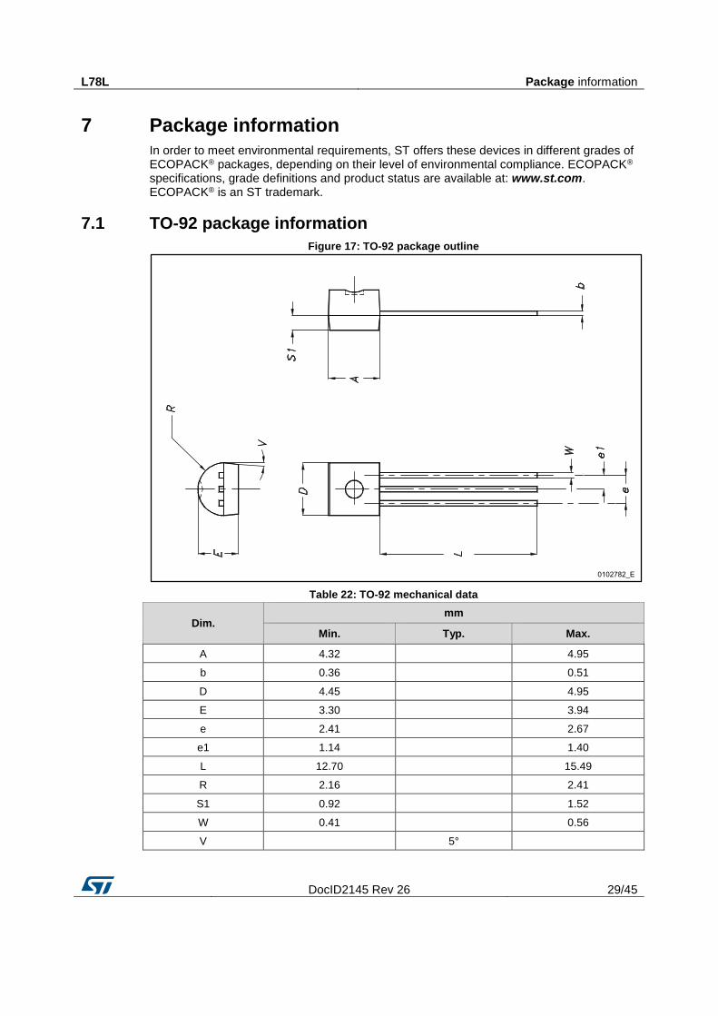
7.1 TO-92 package information
Figure 17: TO-92 package outline
Table 22: TO-92 mechanical data
Dim. mm
Min. Typ. Max.
A 4.32
4.95
b 0.36
0.51
D 4.45
4.95
E 3.30
3.94
e 2.41
2.67
e1 1.14
1.40
L 12.70
15.49
R 2.16
2.41
S1 0.92
1.52
W 0.41
0.56
V
5°
Package information L78L
30/45 DocID2145 Rev 26
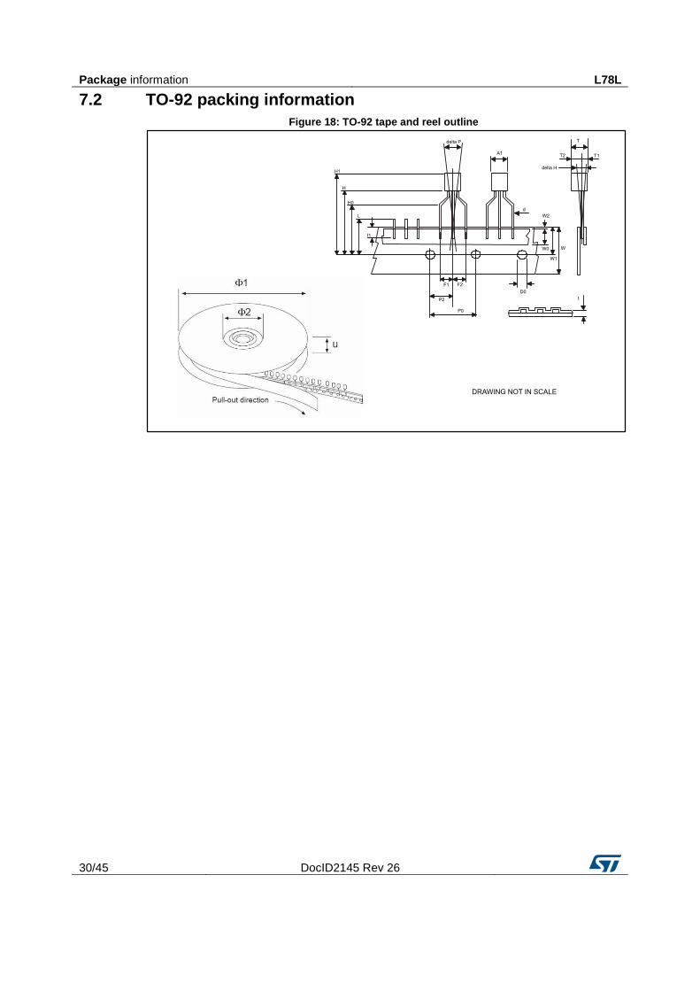
7.2 TO-92 packing information
Figure 18: TO-92 tape and reel outline
L78L Package information
DocID2145 Rev 26 31/45
Table 23: TO-92 tape and reel mechanical data
Dim. mm
Min. Typ. Max.
A1
4.80
T
3.80
T1
1.60
T2
2.30
d 0.45 0.47 0.48
P0 12.50 12.70 12.90
P2 5.65 6.35 7.05
F1, F2 2.40 2.50 2.94
F3 4.98 5.08 5.48
delta H -2.00
2.00
W 17.50 18.00 19.00
W0 5.5 6.00 6.5
W1 8.50 9.00 9.25
W2
0.50
H
18.50 21
H3 0.5 1 2
H0 15.50 16.00 18.8
H1
25.0 27.0
D0 3.80 4.00 4.20
t
0.90
L
11.00
I1 3.00
delta P -1.00
1.00
Ø1 352 355 358
Ø2 28 30 32
u 44 47 50
Package information L78L
32/45 DocID2145 Rev 26
7.3 TO-92 Ammopak packing information
Figure 19: TO-92 Ammopak tape and reel outline
L78L Package information
DocID2145 Rev 26 33/45
Table 24: TO-92 Ammopak tape and reel mechanical data
Dim. mm
Min. Typ. Max.
A1
4.80
T
3.80
T1
1.60
T2
2.30
d 0.45 0.47 0.48
P0 12.50 12.70 12.90
P2 5.65 6.35 7.05
F1, F2 2.40 2.50 2.94
F3 4.98 5.08 5.48
delta H -2.00
2.00
W 17.50 18.00 19.00
W0 5.5 6.00 6.5
W1 8.50 9.00 9.25
W2
0.50
H
18.50 21
H3 0.5 1 2
H0 15.50 16.00 18.8
H1
25.0 27.0
D0 3.80 4.00 4.20
t
0.90
L
11.00
I1 3.00
delta P -1.00
1.00
Package information L78L
34/45 DocID2145 Rev 26
7.4 SO-8 package information
Figure 20: SO-8 package outline
L78L Package information
DocID2145 Rev 26 35/45
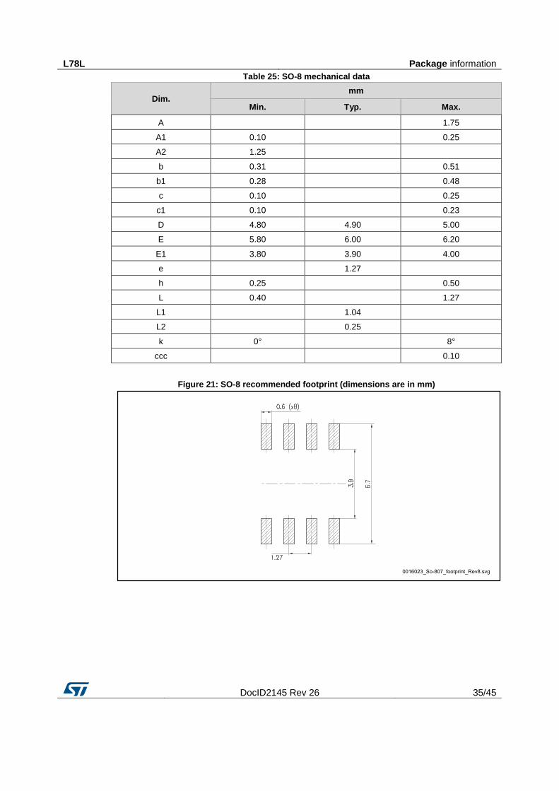
Table 25: SO-8 mechanical data
Dim. mm
Min. Typ. Max.
A
1.75
A1 0.10
0.25
A2 1.25
b 0.31
0.51
b1 0.28
0.48
c 0.10
0.25
c1 0.10
0.23
D 4.80 4.90 5.00
E 5.80 6.00 6.20
E1 3.80 3.90 4.00
e
1.27
h 0.25
0.50
L 0.40
1.27
L1
1.04
L2
0.25
k 0°
8°
ccc
0.10
Figure 21: SO-8 recommended footprint (dimensions are in mm)
Package information L78L
36/45 DocID2145 Rev 26
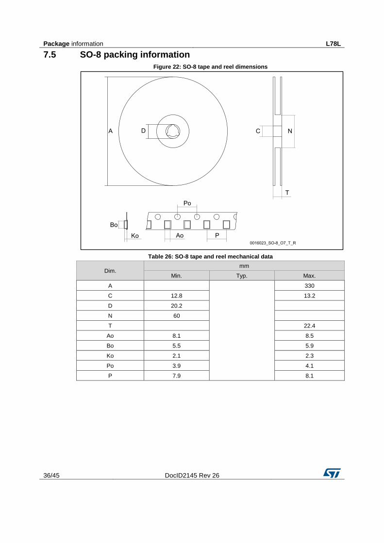
7.5 SO-8 packing information
Figure 22: SO-8 tape and reel dimensions
Table 26: SO-8 tape and reel mechanical data
Dim. mm
Min. Typ. Max.
A
330
C 12.8 13.2
D 20.2
N 60
T
22.4
Ao 8.1 8.5
Bo 5.5 5.9
Ko 2.1 2.3
Po 3.9 4.1
P 7.9 8.1
L78L Package information
DocID2145 Rev 26 37/45
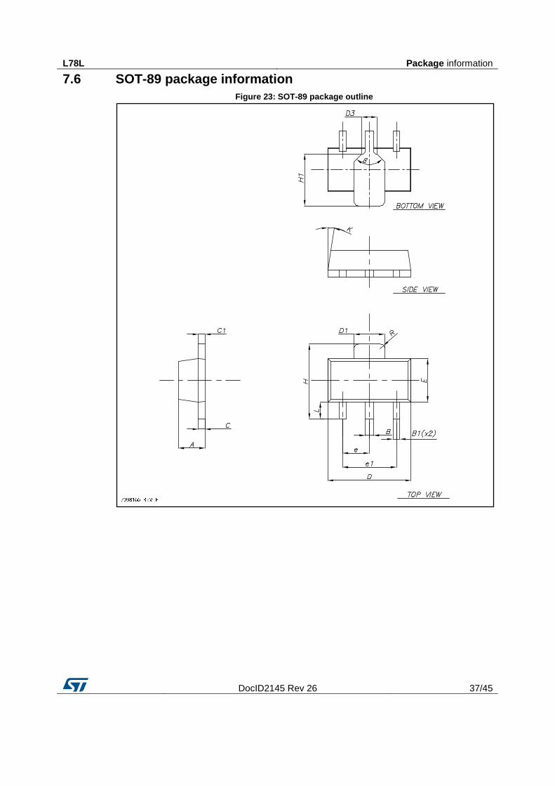
7.6 SOT-89 package information
Figure 23: SOT-89 package outline
Package information L78L
38/45 DocID2145 Rev 26
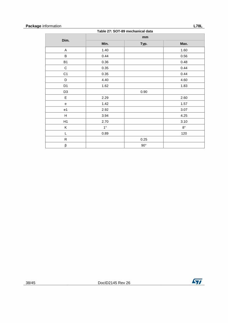
Table 27: SOT-89 mechanical data
Dim. mm
Min. Typ. Max.
A 1.40
1.60
B 0.44
0.56
B1 0.36
0.48
C 0.35
0.44
C1 0.35
0.44
D 4.40
4.60
D1 1.62
1.83
D3
0.90
E 2.29
2.60
e 1.42
1.57
e1 2.92
3.07
H 3.94
4.25
H1 2.70
3.10
K 1°
8°
L 0.89
120
R
0.25
β
90°
L78L Package information
DocID2145 Rev 26 39/45
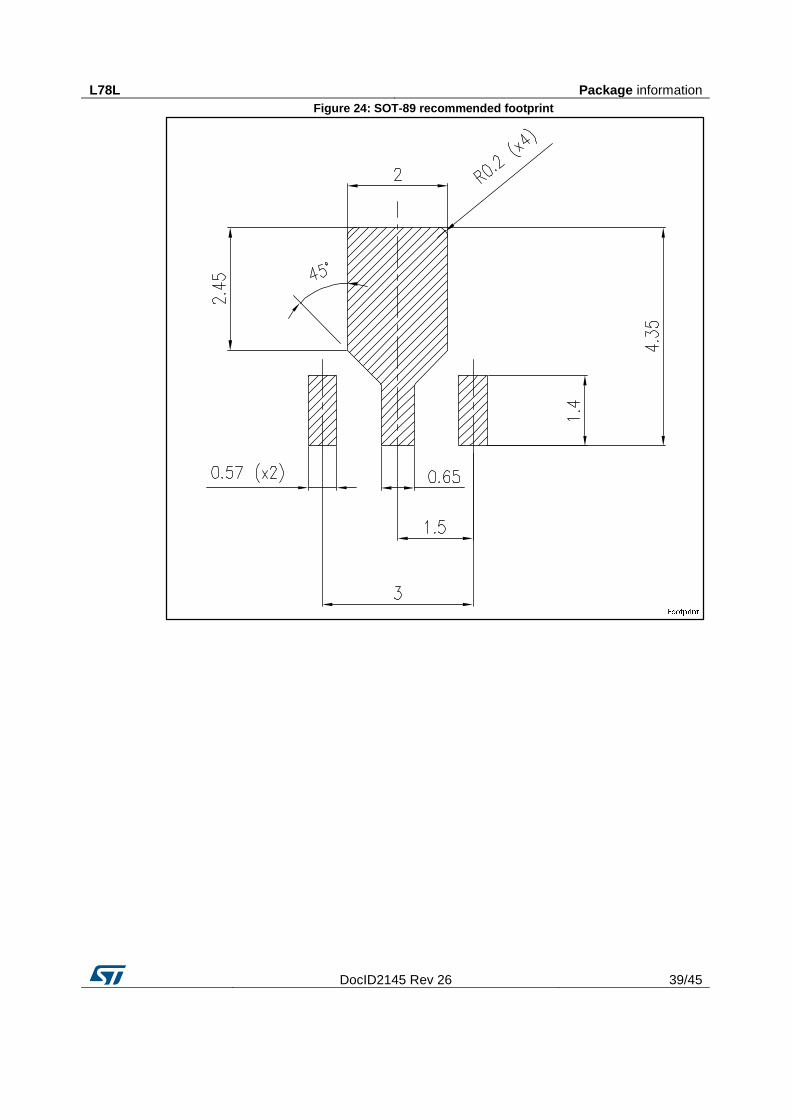
Figure 24: SOT-89 recommended footprint
Package information L78L
40/45 DocID2145 Rev 26
7.7 SOT-89 packing information
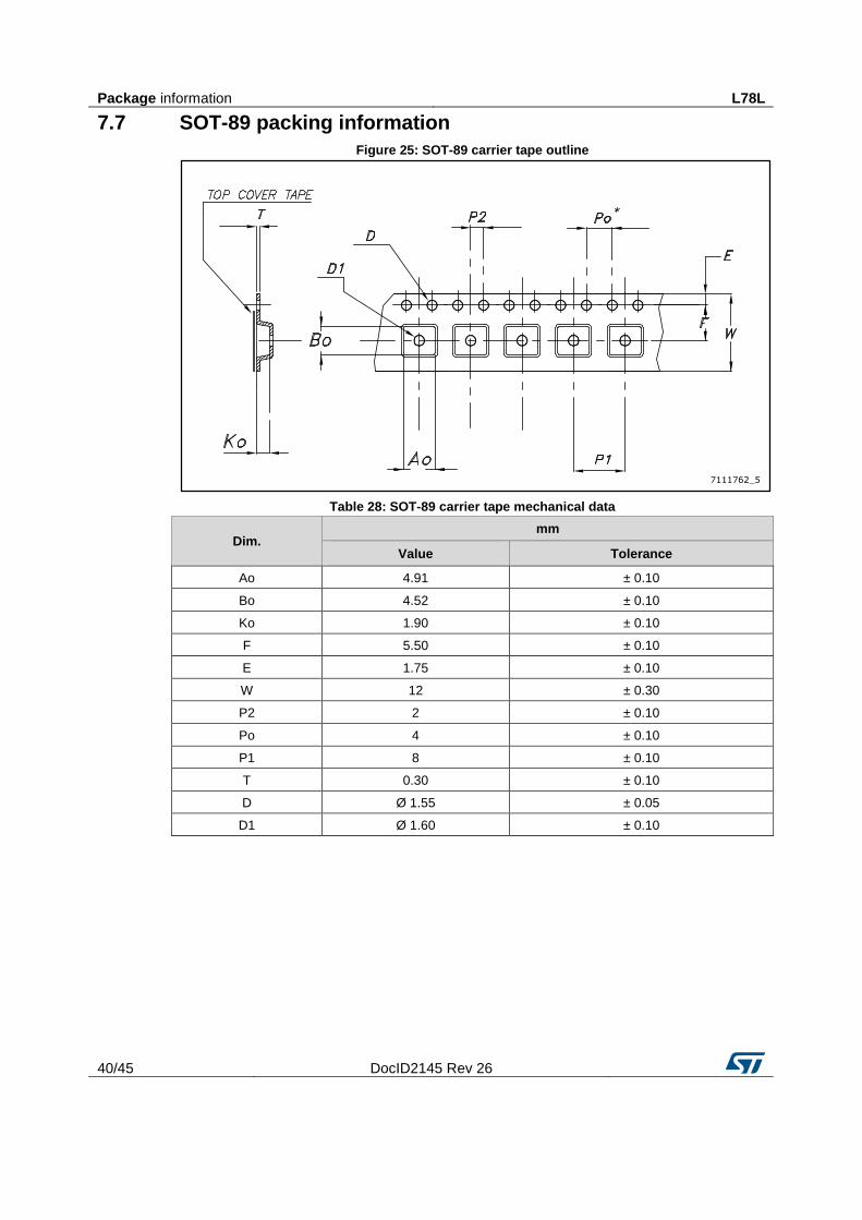
Figure 25: SOT-89 carrier tape outline
Table 28: SOT-89 carrier tape mechanical data
Dim. mm
Value Tolerance
Ao 4.91 ± 0.10
Bo 4.52 ± 0.10
Ko 1.90 ± 0.10
F 5.50 ± 0.10
E 1.75 ± 0.10
W 12 ± 0.30
P2 2 ± 0.10
Po 4 ± 0.10
P1 8 ± 0.10
T 0.30 ± 0.10
D Ø 1.55 ± 0.05
D1 Ø 1.60 ± 0.10
L78L Ordering information
DocID2145 Rev 26 41/45
8 Ordering information Table 29: Order codes
Part numbers Output
voltages
(V) SO-8 TO-92 (Bag) (1) TO-92
(ammopack)
TO-92
(tape and reel) SOT-89
L78L33ABD-TR
L78L33ABZ-AP
L78L33ABUTR 3.3
L78L33ACD13TR L78L33ACZ L78L33ACZ-AP L78L33ACZTR L78L33ACUTR 3.3
L78L33CD-TR
3.3
L78L05ABD13TR L78L05ABZ L78L05ABZ-AP L78L05ABZ-TR L78L05ABUTR 5
L78L05ACD13TR L78L05ACZ L78L05ACZ-AP L78L05ACZTR L78L05ACUTR 5
L78L05CD13TR L78L05CZ
5
L78L06ABZ
L78L06ABUTR 6
L78L06ACD13TR
L78L06ACUTR 6
L78L08ABD13TR
L78L08ABZ-AP L78L08ABZTR L78L08ABUTR 8
L78L08ACD13TR L78L08ACZ L78L08ACZ-AP L78L08ACZTR L78L08ACUTR 8
L78L08CD13TR
8
L78L09ABD13TR L78L09ABZ
L78L09ABUTR 9
L78L09ACD13TR
L78L09ACZ-AP L78L09ACZ-TR L78L09ACUTR 9
L78L09CD13TR
9
L78L10ACUTR 10
L78L12ABD-TR L78L12ABZ L78L12ABZ-AP
L78L12ABUTR 12
L78L12ACD13TR L78L12ACZ L78L12ACZ-AP L78L12ACZ-TR L78L12ACUTR 12
L78L12CD13TR
12
L78L15ABZ-AP
L78L15ABUTR 15
L78L15ACD13TR L78L15ACZ
L78L15ACUTR 15
L78L15CD-TR
15
L78L18ACUTR 18
L78L18CD13TR
18
L78L24ABZ-TR
24
L78L24ACZ-AP L78L24ACUTR 24
L78L24CD-TR
24
Notes:
(1)Available in Ammopak with the suffix "-AP" or in tape and reel with the suffix "TR". Please note that in these cases pins are shaped according to tape and reel specifications.
Ordering information L78L
42/45 DocID2145 Rev 26
Table 30: Marking information
Part numbers Marking Packages Output voltages
L78L05ABD13TR 78L05B SO-8 5 V
L78L05ABUTR 8C SOT-89 5 V
L78L05ABZ L78L05A TO-92 5 V
L78L05ABZ-AP L78L05A TO-92 5 V
L78L05ABZ-TR L78L05A TO-92 5 V
L78L05ACD13TR 78L05A SO-8 5 V
L78L05ACUTR 8C SOT-89 5 V
L78L05ACZ L78L05A TO-92 5 V
L78L05ACZ-AP L78L05A TO-92 5 V
L78L05ACZTR L78L05A TO-92 5 V
L78L05CD13TR 78L05 SO-8 5 V
L78L05CZ L78L05A TO-92 5 V
L78L06ABUTR 8E SOT-89 6 V
L78L06ABZ L78L06A TO-92 6 V
L78L06ACD13TR L78L06A SO-8 6 V
L78L06ACUTR 8E SOT-89 6 V
L78L08ABD13TR 78L08B SO-8 8 V
L78L08ABUTR 8G SOT-89 8 V
L78L08ABZ-AP L78L08A TO-92 8 V
L78L08ABZTR L78L08A TO-92 8 V
L78L08ACD13TR 78L08A SO-8 8 V
L78L08ACUTR 8G SOT-89 8 V
L78L08ACZ L78L08A TO-92 8 V
L78L08ACZ-AP L78L08A TO-92 8 V
L78L08ACZTR L78L08A TO-92 8 V
L78L08CD13TR 78L08 SO-8 8 V
L78L09ABD13TR 78L09B SO-8 8 V
L78L09ABZ L78L09A TO-92 9 V
L78L09ABUTR 8H SOT-89 9 V
L78L09ACD13TR 78L09A SO8 9 V
L78L09ACUTR 8H SOT-89 9 V
L78L09ACZ-AP L78L09A TO-92 9 V
L78L09ACZ-TR L78L09A TO-92 9 V
L78L09CD13TR L78L09A SO-8 9 V
L78L10ACUTR 8I SOT-89 10 V
L78L12ABD-TR 78L12B SO-8 12 V
L78L12ABUTR 8K SOT-89 12 V
L78L12ABZ L78L12A TO-92 12 V
L78L12ABZ-AP L78L12A TO 92 12 V
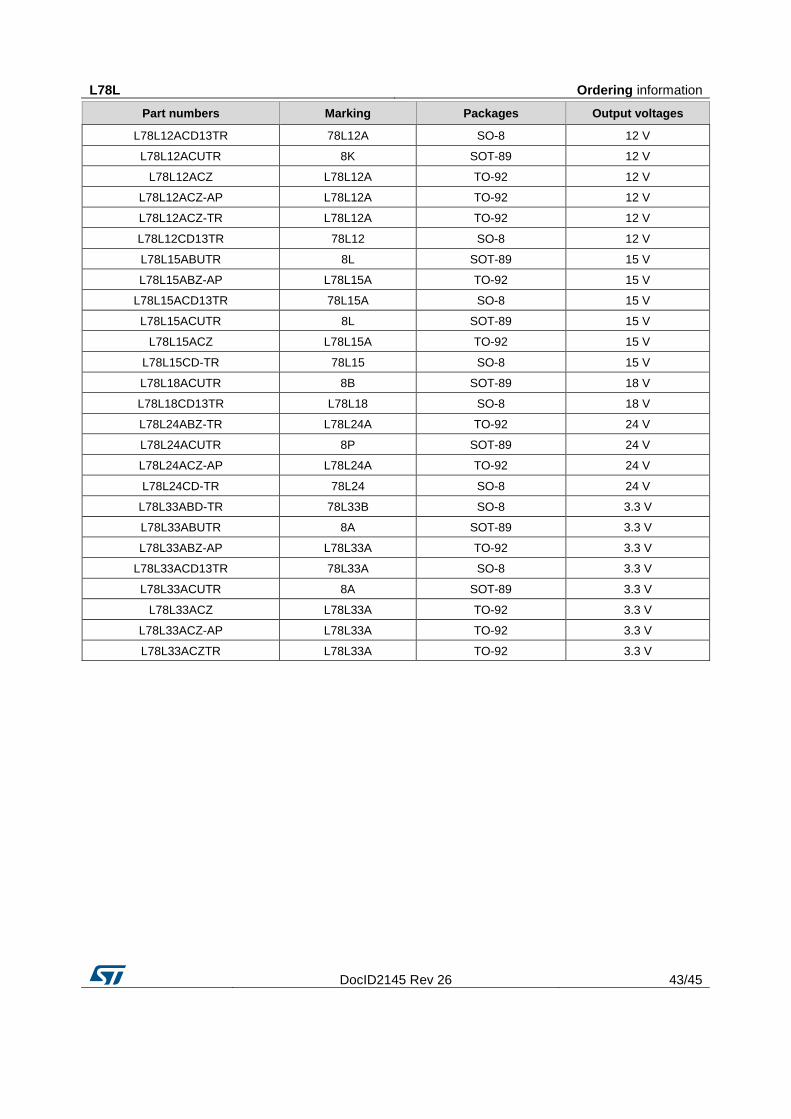
L78L Ordering information
DocID2145 Rev 26 43/45
Part numbers Marking Packages Output voltages
L78L12ACD13TR 78L12A SO-8 12 V
L78L12ACUTR 8K SOT-89 12 V
L78L12ACZ L78L12A TO-92 12 V
L78L12ACZ-AP L78L12A TO-92 12 V
L78L12ACZ-TR L78L12A TO-92 12 V
L78L12CD13TR 78L12 SO-8 12 V
L78L15ABUTR 8L SOT-89 15 V
L78L15ABZ-AP L78L15A TO-92 15 V
L78L15ACD13TR 78L15A SO-8 15 V
L78L15ACUTR 8L SOT-89 15 V
L78L15ACZ L78L15A TO-92 15 V
L78L15CD-TR 78L15 SO-8 15 V
L78L18ACUTR 8B SOT-89 18 V
L78L18CD13TR L78L18 SO-8 18 V
L78L24ABZ-TR L78L24A TO-92 24 V
L78L24ACUTR 8P SOT-89 24 V
L78L24ACZ-AP L78L24A TO-92 24 V
L78L24CD-TR 78L24 SO-8 24 V
L78L33ABD-TR 78L33B SO-8 3.3 V
L78L33ABUTR 8A SOT-89 3.3 V
L78L33ABZ-AP L78L33A TO-92 3.3 V
L78L33ACD13TR 78L33A SO-8 3.3 V
L78L33ACUTR 8A SOT-89 3.3 V
L78L33ACZ L78L33A TO-92 3.3 V
L78L33ACZ-AP L78L33A TO-92 3.3 V
L78L33ACZTR L78L33A TO-92 3.3 V
Revision history L78L
44/45 DocID2145 Rev 26
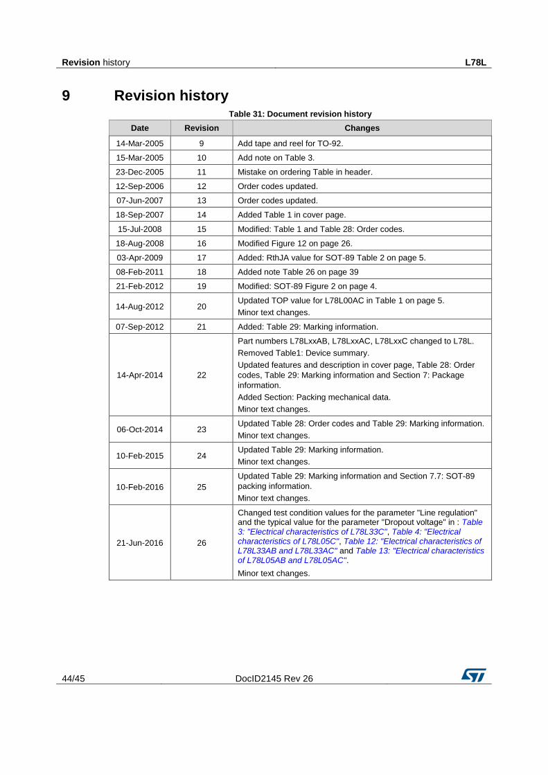
9 Revision history Table 31: Document revision history
Date Revision Changes
14-Mar-2005 9 Add tape and reel for TO-92.
15-Mar-2005 10 Add note on Table 3.
23-Dec-2005 11 Mistake on ordering Table in header.
12-Sep-2006 12 Order codes updated.
07-Jun-2007 13 Order codes updated.
18-Sep-2007 14 Added Table 1 in cover page.
15-Jul-2008 15 Modified: Table 1 and Table 28: Order codes.
18-Aug-2008 16 Modified Figure 12 on page 26.
03-Apr-2009 17 Added: RthJA value for SOT-89 Table 2 on page 5.
08-Feb-2011 18 Added note Table 26 on page 39
21-Feb-2012 19 Modified: SOT-89 Figure 2 on page 4.
14-Aug-2012 20 Updated TOP value for L78L00AC in Table 1 on page 5.
Minor text changes.
07-Sep-2012 21 Added: Table 29: Marking information.
14-Apr-2014 22
Part numbers L78LxxAB, L78LxxAC, L78LxxC changed to L78L.
Removed Table1: Device summary.
Updated features and description in cover page, Table 28: Order
codes, Table 29: Marking information and Section 7: Package
information.
Added Section: Packing mechanical data.
Minor text changes.
06-Oct-2014 23 Updated Table 28: Order codes and Table 29: Marking information.
Minor text changes.
10-Feb-2015 24 Updated Table 29: Marking information.
Minor text changes.
10-Feb-2016 25
Updated Table 29: Marking information and Section 7.7: SOT-89
packing information.
Minor text changes.
21-Jun-2016 26
Changed test condition values for the parameter "Line regulation" and the typical value for the parameter "Dropout voltage" in : Table 3: "Electrical characteristics of L78L33C", Table 4: "Electrical characteristics of L78L05C", Table 12: "Electrical characteristics of L78L33AB and L78L33AC" and Table 13: "Electrical characteristics of L78L05AB and L78L05AC".
Minor text changes.
L78L
DocID2145 Rev 26 45/45
IMPORTANT NOTICE – PLEASE READ CAREFULLY
STMicroelectronics NV and its subsidiaries (“ST”) reserve the right to make changes, corrections, enhancements, modifications, and improvements to ST products and/or to this document at any time without notice. Purchasers should obtain the latest relevant information on ST products before placing orders. ST products are sold pursuant to ST’s terms and conditions of sale in place at the time of order acknowledgement.
Purchasers are solely responsible for the choice, selection, and use of ST products and ST assumes no liability for application assistance or the design of Purchasers’ products.
No license, express or implied, to any intellectual property right is granted by ST herein.
Resale of ST products with provisions different from the information set forth herein shall void any warranty granted by ST for such product.
ST and the ST logo are trademarks of ST. All other product or service names are the property of their respective owners.
Information in this document supersedes and replaces information previously supplied in any prior versions of this document.
© 2016 STMicroelectronics – All rights reserved