Embed Size (px)
Citation preview
DC-DC Converter Control Circuits MC34063A/B
July 2013 - Rev. 1.1 - 1 - HTC
FEATURES
Output Switch Current In Excess of 1.5A
2% Reference Accuracy
Low Quiescent Current : 2.5mA(Typ.)
Operating From 3V to 40V
Frequency Operation to 100KHz
Active Current Limiting
Moisture Sensitivity Level 3D
MC34063AG is Halogen Free Products
APPLICATION
Battery Chargers
NICs / Switches / Hubs
ADSL Modems
Negative Voltage Power Supplies
DESCRIPTION
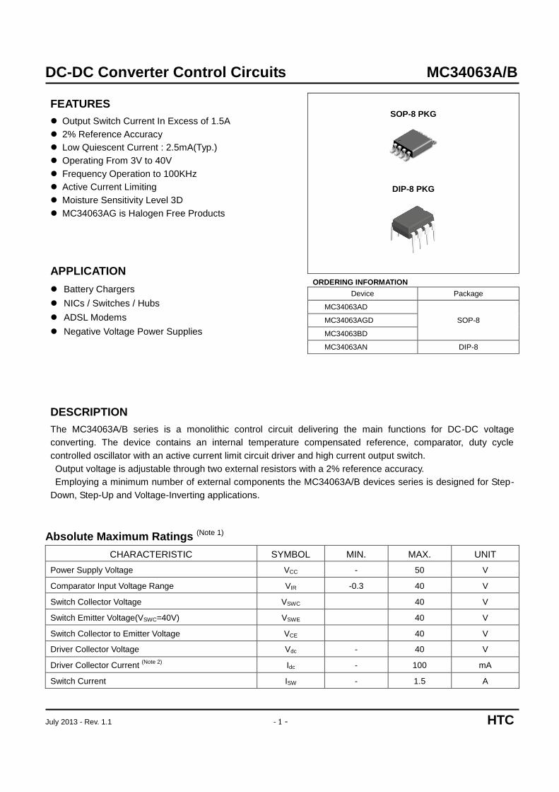
SOP-8 PKG
DIP-8 PKG
ORDERING INFORMATION
Device Package
MC34063AD
SOP-8 MC34063AGD
MC34063BD
MC34063AN DIP-8
The MC34063A/B series is a monolithic control circuit delivering the main functions for DC-DC voltage
converting. The device contains an internal temperature compensated reference, comparator, duty cycle
controlled oscillator with an active current limit circuit driver and high current output switch.
Output voltage is adjustable through two external resistors with a 2% reference accuracy.
Employing a minimum number of external components the MC34063A/B devices series is designed for Step-
Down, Step-Up and Voltage-Inverting applications.
Absolute Maximum Ratings (Note 1)
CHARACTERISTIC SYMBOL MIN. MAX. UNIT
Power Supply Voltage VCC - 50 V
Comparator Input Voltage Range VIR -0.3 40 V
Switch Collector Voltage VSWC 40 V
Switch Emitter Voltage(VSWC=40V) VSWE 40 V
Switch Collector to Emitter Voltage VCE 40 V
Driver Collector Voltage Vdc - 40 V
Driver Collector Current (Note 2)
Idc - 100 mA
Switch Current ISW - 1.5 A
DC-DC Converter Control Circuits MC34063A/B
July 2013 - Rev. 1.1 - 2 - HTC
Absolute Maximum Ratings (Continued)
CHARACTERISTIC SYMBOL MIN. MAX. UNIT
Power Dissipation (at TA = 25°C) SOP-8 PDMAX_SOP-8 0.625 W
DIP-8 PDMAX_DIP-8 1.0 W
Thermal Resistance(*) SOP-8 θJA-SOP-8 160 °C/W
DIP-8 θJA-DIP-8 100 °C/W
Operating Junction Temperature Range TJ -40 150 °C
Operating Ambient Temperature Range MC34063A
TAOPR 0 75 °C
MC34063B -40 85 °C
Storage Temperature Range TSTG -65 150 °C
Note 1. Absolute Maximum Ratings are those values beyond which damage to the device may occur. Functional operation under these
conditions is not implied.
(*) This value depends from thermal design of PCB on which the device is mounted.
Ordering Information
Operating Ambient Temperature(TAOPR) Range Package Order No. Supplied As Status
0~70
SOP8
MC34063AD Reel Active
0~70 MC34063AGD Reel Contact us
-40~85 MC34063BD Reel Active
0~70 DIP8
MC34063AN Tube Active
-40~85 MC34063BN Tube Active
Package Type
Root Name
Product Code
MC 34063
D
N
: SOP8
: DIP8
Temperature RangeA
B
: 0~70
: -40~85
Green ModeG
Blank
: Halogen Free
: Pb Free
DC-DC Converter Control Circuits MC34063A/B
July 2013 - Rev. 1.1 - 3 - HTC
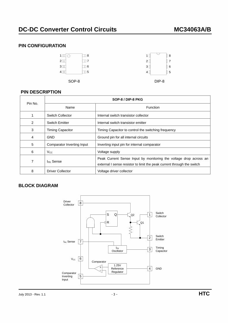
PIN CONFIGURATION
SOP-8 DIP-8
PIN DESCRIPTION
Pin No. SOP-8 / DIP-8 PKG
Name Function
1 Switch Collector Internal switch transistor collector
2 Switch Emitter Internal switch transistor emitter
3 Timing Capacitor Timing Capacitor to control the switching frequency
4 GND Ground pin for all internal circuits
5 Comparator Inverting Input Inverting input pin for internal comparator
6 VCC Voltage supply
7 IPK Sense Peak Current Sense Input by monitoring the voltage drop across an
external I sense resistor to limit the peak current through the switch
8 Driver Collector Voltage driver collector
BLOCK DIAGRAM
1
2
3
4
8
7
6
5
1
2
3
4
8
7
6
5
S Q
R
Q2
IPK
Oscillator
1.25V
Reference
Regulator
Q1
3
2
4
1
7
6
5
8
+-
Comparator
Driver
Collector
IPK Sense
VCC
Comparator
Inverting
Input
Switch
Collector
Switch
Emitter
Timing
Capacitor
GND
DC-DC Converter Control Circuits MC34063A/B
July 2013 - Rev. 1.1 - 4 - HTC
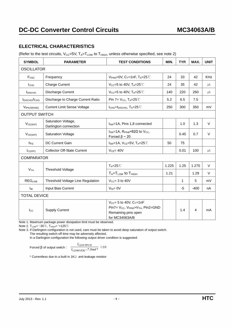
ELECTRICAL CHARACTERISTICS
(Refer to the test circuits, VCC=5V, TA=TLOW to THIGH, unless otherwise specified, see note 2)
SYMBOL PARAMETER TEST CONDITIONS MIN. TYP. MAX. UNIT
OSCILLATOR
FOSC Frequency VPIN5=0V, CT=1nF, TA=25 24 33 42 KHz
ICHG Charge Current VCC=5 to 40V, TA=25 24 35 42
IDISCHG Discharge Current VCC=5 to 40V, TA=25 140 220 260
IDISCHG/ICHG Discharge to Charge Current Ratio Pin 7= VCC, TA=25 5.2 6.5 7.5
VIPK(SENSE) Current Limit Sense Voltage ICHG=IDISCHG, TA=25 250 300 350 mV
OUTPUT SWITCH
VCE(SAT) Saturation Voltage,
Darlington connection ISW=1A, Pins 1,8 connected 1.0 1.3 V
VCE(SAT) Saturation Voltage ISW=1A, RPIN8=82Ω to VCC,
Forced β ~ 20 0.45 0.7 V
hFE DC Current Gain ISW=1A, VCE=5V, TA=25 50 75
IC(OFF) Collector Off-State Current VCE= 40V 0.01 100
COMPARATOR
VTH Threshold Voltage TA=25 1.225 1.25 1.275 V
TA=TLOW to THIGH 1.21 1.29 V
REGLINE Threshold Voltage Line Regulation VCC= 3 to 40V 1 5 mV
IIB Input Bias Current VIN= 0V -5 -400 nA
TOTAL DEVICE
ICC Supply Current
VCC= 5 to 40V, CT=1nF
Pin7= VCC, VPIN5>VTH, Pin2=GND
Remaining pins open
for MC34063A/B
1.4 4 mA
Note 1. Maximum package power dissipation limit must be observed.
Note 2. TLOW= '-30, THIGH= '+125
Note 3. If Darlington configuration is not used, care must be taken to avoid deep saturation of output switch.
The resulting switch-off time may be adversely affected.
In a Darlington configuration the following output driver condition is suggested:
Forced β of output switch : 10*7.0mΑ-Ι
Ι
C(DRIVER)
C(OUTPUT)≥
* Currentless due to a built in 1KΩ anti-leakage resistor
DC-DC Converter Control Circuits MC34063A/B
July 2013 - Rev. 1.1 - 5 - HTC
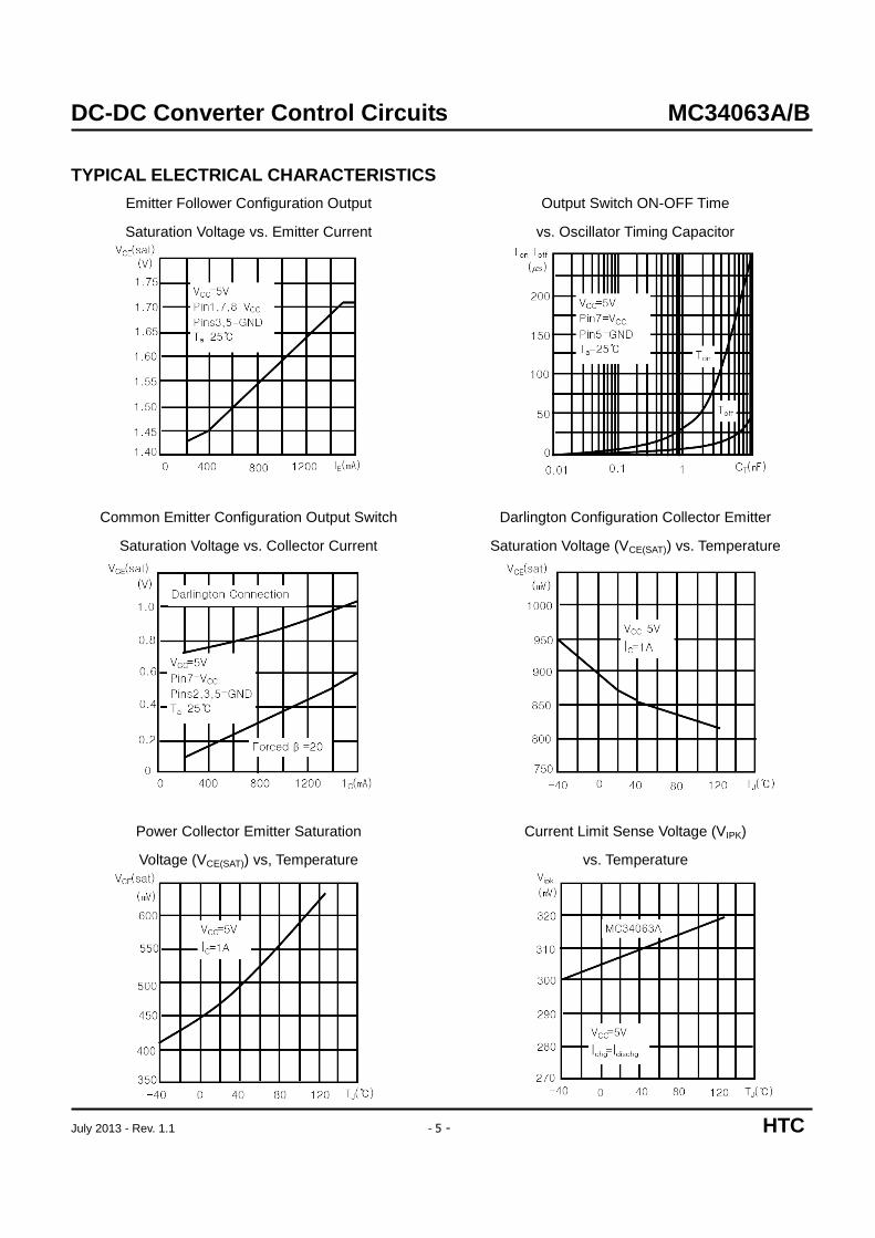
TYPICAL ELECTRICAL CHARACTERISTICS
Emitter Follower Configuration Output
Saturation Voltage vs. Emitter Current
Common Emitter Configuration Output Switch
Saturation Voltage vs. Collector Current
Power Collector Emitter Saturation
Voltage (VCE(SAT)) vs, Temperature
Output Switch ON-OFF Time
vs. Oscillator Timing Capacitor
Darlington Configuration Collector Emitter
Saturation Voltage (VCE(SAT)) vs. Temperature
Current Limit Sense Voltage (VIPK)
vs. Temperature
DC-DC Converter Control Circuits MC34063A/B
July 2013 - Rev. 1.1 - 6 - HTC
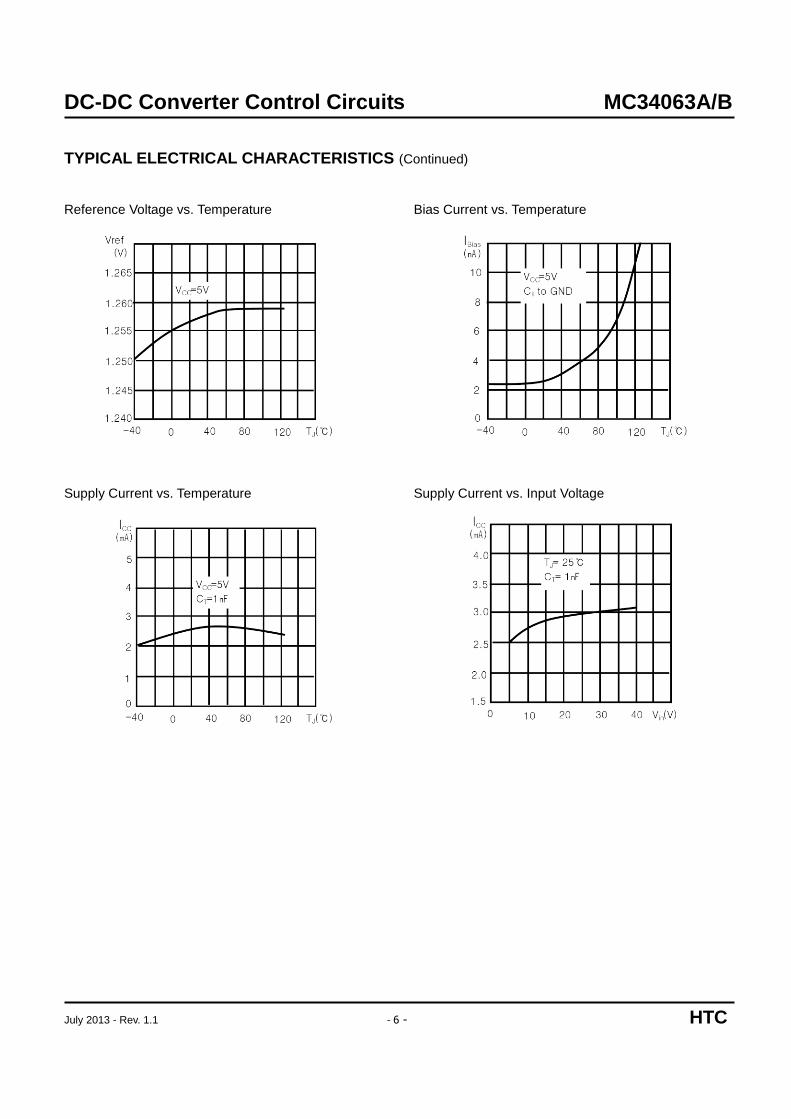
TYPICAL ELECTRICAL CHARACTERISTICS (Continued)
Reference Voltage vs. Temperature
Supply Current vs. Temperature
Bias Current vs. Temperature
Supply Current vs. Input Voltage
DC-DC Converter Control Circuits MC34063A/B
July 2013 - Rev. 1.1 - 7 - HTC
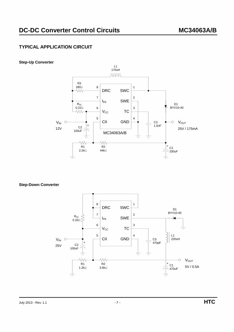
TYPICAL APPLICATION CIRCUIT
Step-Up Converter
Step-Down Converter
RSC
0.22Ω
R3
180Ω
C2
100uF
R1
2.2kΩ
R2
44kΩ
C3
1.5nF
D1
BYV10-40
C1
330uF
DRC
IPK
VCC
CII
SWC
SWE
TC
GND
L1
170uH
1
2
3
4
8
7
6
5
VIN
12V
VOUT
25V / 175mA
+
+
MC34063A/B
C2
100uF
R1
1.2kΩ
R2
3.6kΩ
C3
470pF
DRC
IPK
VCC
CII
SWC
SWE
TC
GND
1
2
3
4
8
7
6
5
VIN
25V
VOUT
5V / 0.5A
RSC
0.33Ω
D1
BYV10-40
C1
470uF
+
+
L1
220uH
DC-DC Converter Control Circuits MC34063A/B
July 2013 - Rev. 1.1 - 8 - HTC
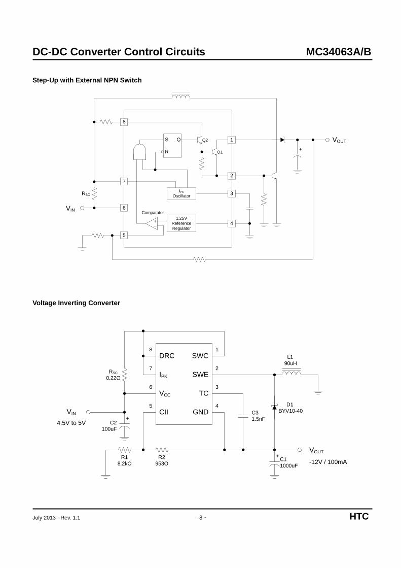
Step-Up with External NPN Switch
Voltage Inverting Converter
S Q
R
Q2
IPK
Oscillator
1.25V
Reference
Regulator
Q1
3
2
4
1
7
6
5
8
+-
Comparator
RSC
+
VIN
VOUT
C2
100uF
R1
8.2kO
R2
953O
C3
1.5nF
DRC
IPK
VCC
CII
SWC
SWE
TC
GND
1
2
3
4
8
7
6
5
VIN
4.5V to 5V
VOUT
-12V / 100mA
RSC
0.22O
D1
BYV10-40
C1
1000uF
+
+
L1
90uH
DC-DC Converter Control Circuits MC34063A/B
July 2013 - Rev. 1.1 - 9 - HTC
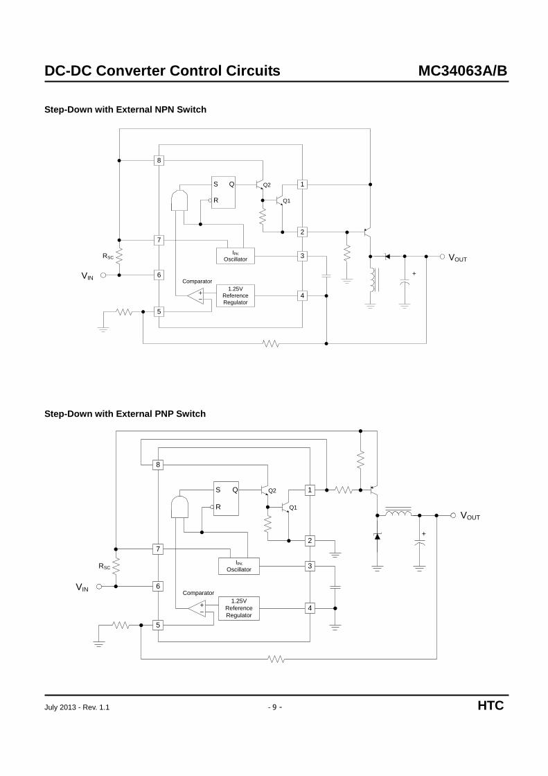
Step-Down with External NPN Switch
Step-Down with External PNP Switch
S Q
R
Q2
IPK
Oscillator
1.25V
Reference
Regulator
Q1
3
2
4
1
7
6
5
8
+-
Comparator
RSC
+
VIN
VOUT
S Q
R
Q2
IPK
Oscillator
1.25V
Reference
Regulator
Q1
3
2
4
1
7
6
5
8
+-
Comparator
RSC
+VIN
VOUT
DC-DC Converter Control Circuits MC34063A/B
July 2013 - Rev. 1.1 - 10 - HTC
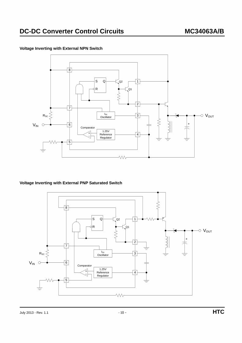
Voltage Inverting with External NPN Switch
Voltage Inverting with External PNP Saturated Switch
S Q
R
Q2
IPK
Oscillator
1.25V
Reference
Regulator
Q1
3
2
4
1
7
6
5
8
+-
Comparator
RSC
VIN
VOUT
+
S Q
R
Q2
IPK
Oscillator
1.25V
Reference
Regulator
Q1
3
2
4
1
7
6
5
8
+-
Comparator
RSC
+
VIN
VOUT
DC-DC Converter Control Circuits MC34063A/B
July 2013 - Rev. 1.1 - 11 - HTC
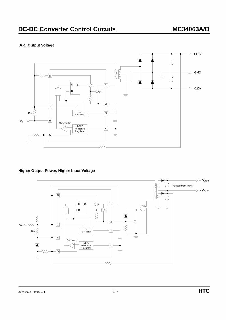
Dual Output Voltage
S Q
R
Q2
IPK
Oscillator
1.25V
Reference
Regulator
Q1
3
2
4
1
7
6
5
8
+-
Comparator
RSC
VIN
+
+
+12V
-12V
GND
Higher Output Power, Higher Input Voltage
S Q
R
Q2
IPK
Oscillator
1.25V
Reference
Regulator
Q1
3
2
4
1
7
6
5
8
+-
Comparator
RSC
VIN
+
+
+ VOUT
- VOUT
Isolated from input
DC-DC Converter Control Circuits MC34063A/B
July 2013 - Rev. 1.1 - 12 - HTC
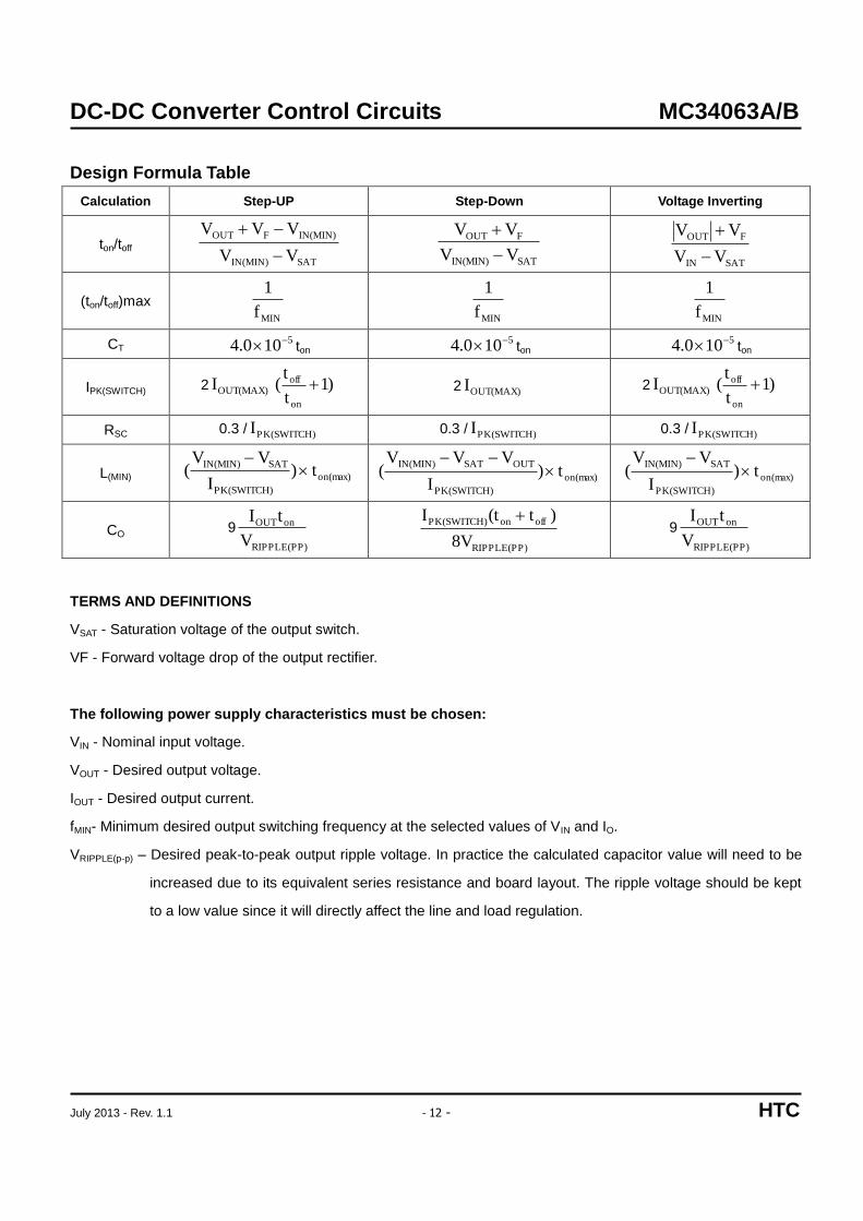
Design Formula Table
Calculation Step-UP Step-Down Voltage Inverting
ton/toff SATIN(MIN)
IN(MIN)FOUT
VV
VVV
SATIN(MIN)
FOUT
VV
VV
SATIN
FOUT
VV
VV
(ton/toff)max MINf
1
MINf
1
MINf
1
CT 5100.4 ton 5100.4 ton
5100.4 ton
IPK(SWITCH) 2 OUT(MAX)I )1t
t(
on
off 2 OUT(MAX)I 2 OUT(MAX)I )1t
t(
on
off
RSC 0.3 / PK(SWITCH)I 0.3 / PK(SWITCH)I 0.3 / PK(SWITCH)I
L(MIN) on(max)
PK(SWITCH)
SATIN(MIN)t)
I
VV(
on(max)
PK(SWITCH)
OUTSATIN(MIN)t)
I
VVV(
on(max)
PK(SWITCH)
SATIN(MIN)t)
I
VV(
CO 9
RIPPLE(PP)
onOUT
V
tI
RIPPLE(PP)
offonPK(SWITCH)
8V
)t(tI 9
RIPPLE(PP)
onOUT
V
tI
TERMS AND DEFINITIONS
VSAT - Saturation voltage of the output switch.
VF - Forward voltage drop of the output rectifier.
The following power supply characteristics must be chosen:
VIN - Nominal input voltage.
VOUT - Desired output voltage.
IOUT - Desired output current.
fMIN- Minimum desired output switching frequency at the selected values of VIN and IO.
VRIPPLE(p-p) – Desired peak-to-peak output ripple voltage. In practice the calculated capacitor value will need to be
increased due to its equivalent series resistance and board layout. The ripple voltage should be kept
to a low value since it will directly affect the line and load regulation.