Embed Size (px)
Citation preview
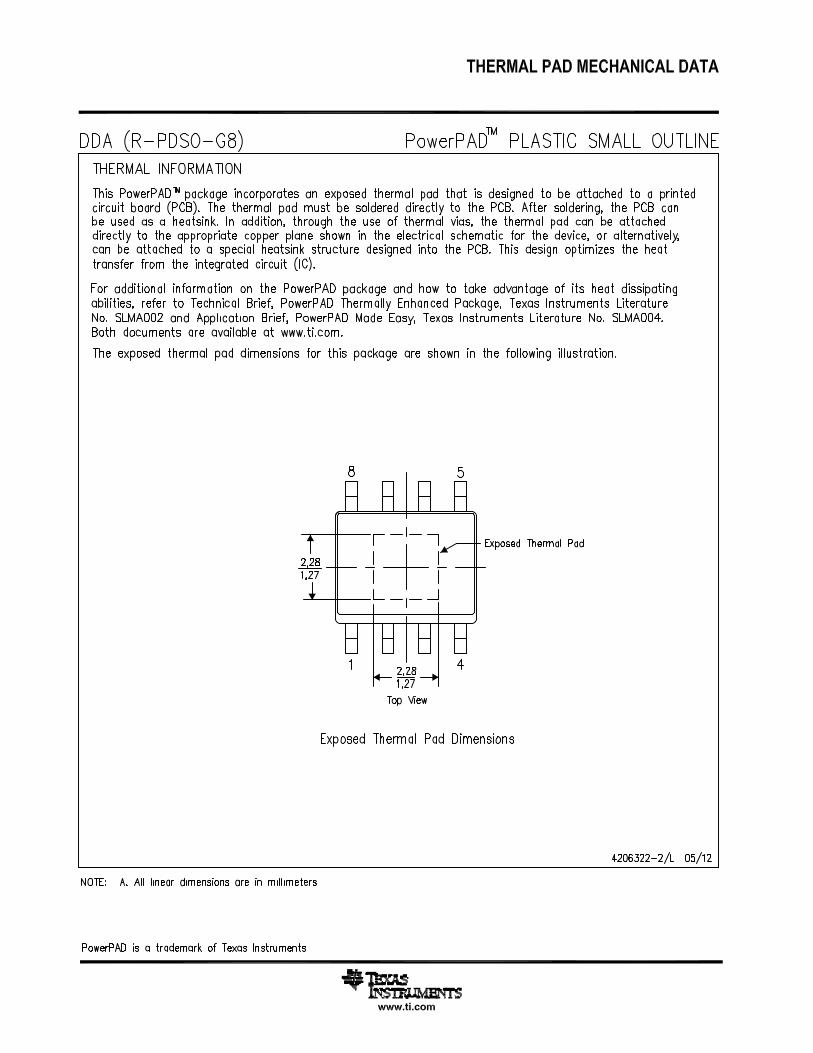
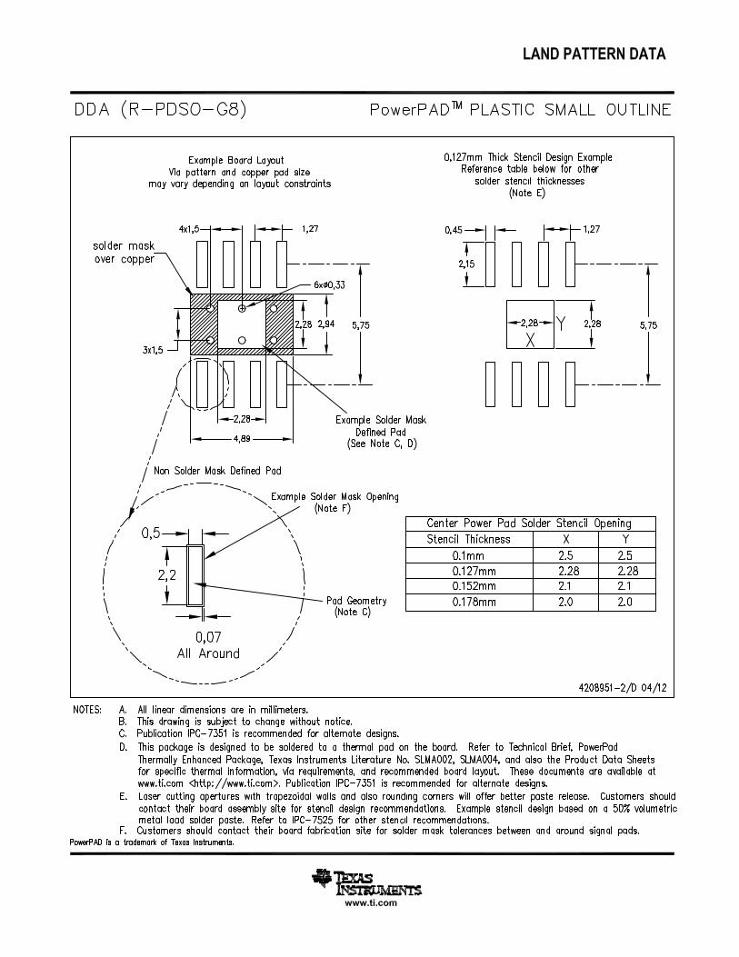
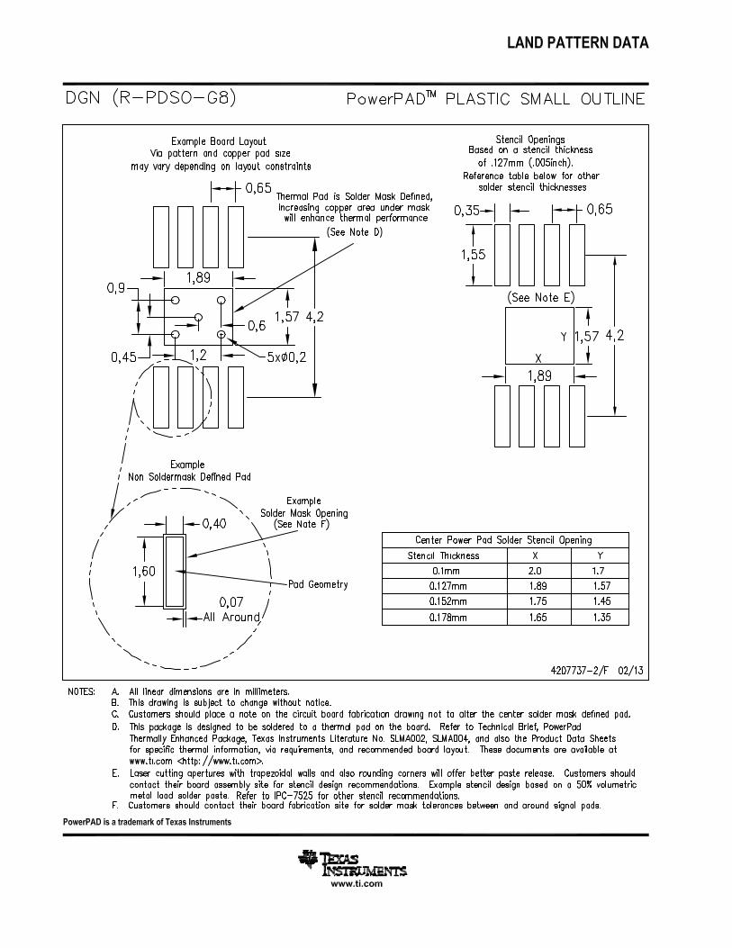
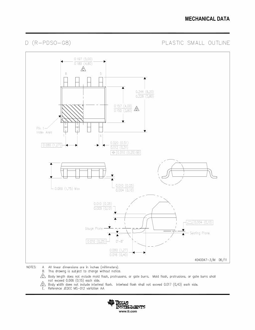
DGN−8DDA−8D−8
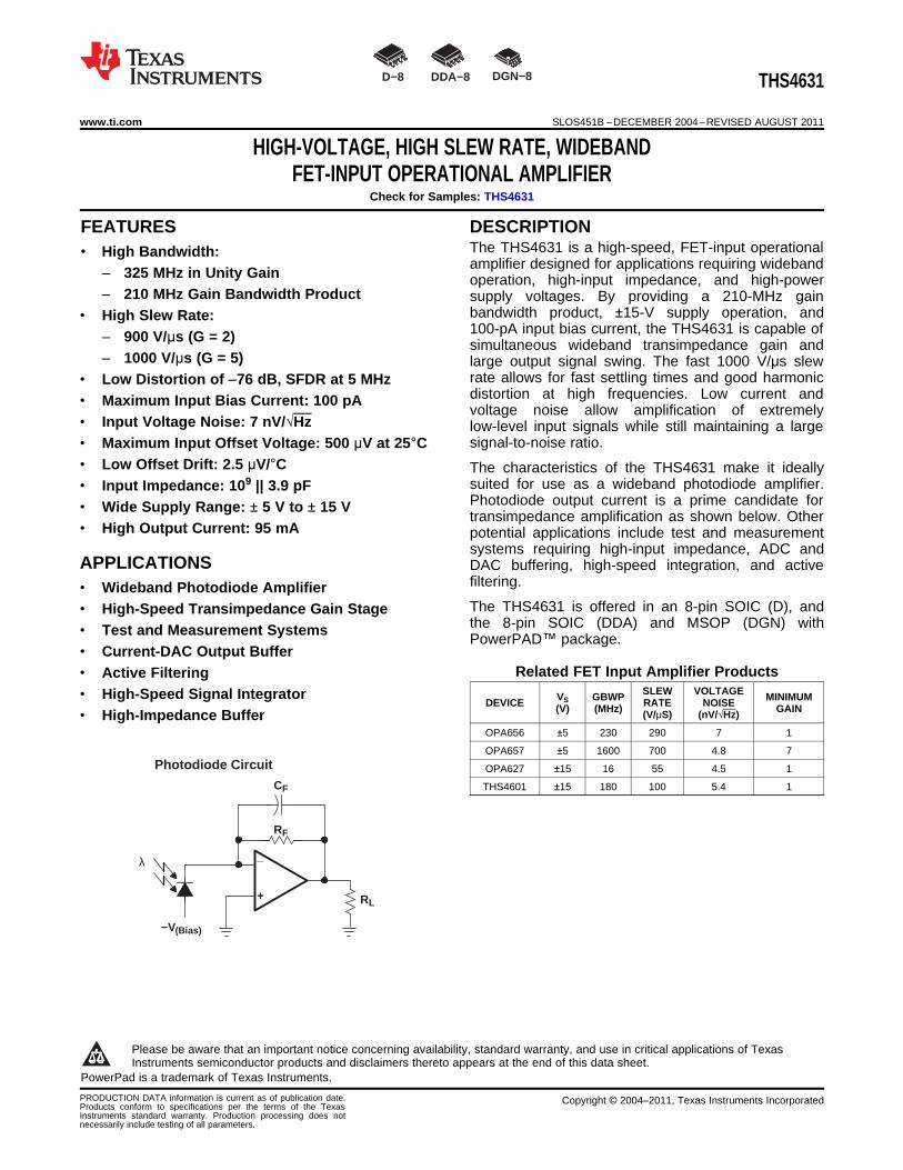
_
+
RF
CF
λ
−V(Bias)
RL
Photodiode Circuit
THS4631
www.ti.com SLOS451B –DECEMBER 2004–REVISED AUGUST 2011
HIGH-VOLTAGE, HIGH SLEW RATE, WIDEBANDFET-INPUT OPERATIONAL AMPLIFIER
Check for Samples: THS4631
1FEATURES DESCRIPTIONThe THS4631 is a high-speed, FET-input operational
2• High Bandwidth:amplifier designed for applications requiring wideband– 325 MHz in Unity Gain operation, high-input impedance, and high-power
– 210 MHz Gain Bandwidth Product supply voltages. By providing a 210-MHz gainbandwidth product, ±15-V supply operation, and• High Slew Rate:100-pA input bias current, the THS4631 is capable of– 900 V/µs (G = 2) simultaneous wideband transimpedance gain and
– 1000 V/µs (G = 5) large output signal swing. The fast 1000 V/µs slewrate allows for fast settling times and good harmonic• Low Distortion of –76 dB, SFDR at 5 MHzdistortion at high frequencies. Low current and• Maximum Input Bias Current: 100 pAvoltage noise allow amplification of extremely
• Input Voltage Noise: 7 nV/√Hz low-level input signals while still maintaining a largesignal-to-noise ratio.• Maximum Input Offset Voltage: 500 µV at 25°C
• Low Offset Drift: 2.5 µV/°C The characteristics of the THS4631 make it ideallysuited for use as a wideband photodiode amplifier.• Input Impedance: 109 || 3.9 pFPhotodiode output current is a prime candidate for• Wide Supply Range: ± 5 V to ± 15 Vtransimpedance amplification as shown below. Other
• High Output Current: 95 mA potential applications include test and measurementsystems requiring high-input impedance, ADC and
APPLICATIONS DAC buffering, high-speed integration, and activefiltering.• Wideband Photodiode AmplifierThe THS4631 is offered in an 8-pin SOIC (D), and• High-Speed Transimpedance Gain Stagethe 8-pin SOIC (DDA) and MSOP (DGN) with• Test and Measurement SystemsPowerPAD™ package.
• Current-DAC Output BufferRelated FET Input Amplifier Products• Active Filtering
SLEW VOLTAGE• High-Speed Signal Integrator VS GBWP MINIMUMDEVICE RATE NOISE(V) (MHz) GAIN(V/µS) (nV/√Hz)• High-Impedance BufferOPA656 ±5 230 290 7 1
OPA657 ±5 1600 700 4.8 7
OPA627 ±15 16 55 4.5 1
THS4601 ±15 180 100 5.4 1
1
Please be aware that an important notice concerning availability, standard warranty, and use in critical applications of TexasInstruments semiconductor products and disclaimers thereto appears at the end of this data sheet.
2PowerPad is a trademark of Texas Instruments.
PRODUCTION DATA information is current as of publication date. Copyright © 2004–2011, Texas Instruments IncorporatedProducts conform to specifications per the terms of the TexasInstruments standard warranty. Production processing does notnecessarily include testing of all parameters.
THS4631
SLOS451B –DECEMBER 2004–REVISED AUGUST 2011 www.ti.com
This integrated circuit can be damaged by ESD. Texas Instruments recommends that all integrated circuits be handled withappropriate precautions. Failure to observe proper handling and installation procedures can cause damage.
ESD damage can range from subtle performance degradation to complete device failure. Precision integrated circuits may be moresusceptible to damage because very small parametric changes could cause the device not to meet its published specifications.
ABSOLUTE MAXIMUM RATINGSover operating free-air temperature range (unless otherwise noted) (1)
UNITS
VS Supply voltage, VS– to VS+ 33 V
VI Input voltage ±VS
IO(2) Output current 150 mA
Continuous power dissipation See Dissipation Rating Table
TJ Maximum junction temperature (2) 150°CTA Operating free-air temperature, continues operation, long-term reliability (2) 125°CTstg Storage temperature range –65°C to 150°C
HBM 1000 V
ESD ratings: CDM 1500 V
MM 100 V
(1) The absolute maximum ratings under any condition is limited by the constraints of the silicon process. Stresses above these ratings maycause permanent damage. Exposure to absolute maximum conditions for extended periods may degrade device reliability. These arestress ratings only, and functional operation of the device at these or any other conditions beyond those specified is not implied.
(2) The maximum junction temperature for continuous operation is limited by package constraints. Operation above this temperature mayresult in reduced reliability and/or lifetime of the device.
PACKAGE DISSIPATION RATINGSPOWER RATING (1) (TJ =125°C)
PACKAGE θJC (°C/W) θJA (°C/W)TA ≤ 25°C TA = 85°C
D (8) (2) 38.3 95 1.1 W 0.47 W
DDA (8) 9.2 45.8 2.3 W 0.98 W
DGN (8) 4.7 58.4 2.14 W 1.11 W
(1) Power rating is determined with a junction temperature of 125°C. This is the point where distortion starts to substantially increase.Thermal management of the final PCB should strive to keep the junction temperature at or below 125°C for best performance.
(2) This data was taken using the JEDEC standard High-K test PCB.
RECOMMENDED OPERATING CONDITIONSover operating free-air temperature range (unless otherwise noted)
MIN MAX UNITS
Dual Supply ±5 ±15VS Supply Voltage V
Single Supply 10 30
TA Operating free-air temperature -40 85 °C
2 Copyright © 2004–2011, Texas Instruments Incorporated
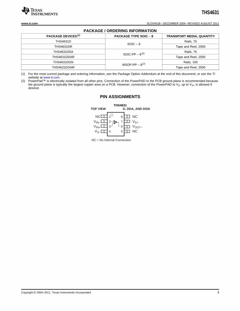
1
2
3
4
8
7
6
5
NCVIN−VIN+
VS−
NCVS+VOUT−
NC
NC = No Internal Connection
TOP VIEW D, DDA, AND DGN
THS4631
www.ti.com SLOS451B –DECEMBER 2004–REVISED AUGUST 2011
PACKAGE / ORDERING INFORMATIONPACKAGE DEVICES (1) PACKAGE TYPE SOIC – 8 TRANSPORT MEDIA, QUANTITY
THS4631D Rails, 75SOIC – 8
THS4631DR Tape and Reel, 2500
THS4631DDA Rails, 75SOIC-PP – 8 (2)
THS4631DDAR Tape and Reel, 2500
THS4631DGN Rails, 100MSOP-PP – 8 (2)
THS4631DGNR Tape and Reel, 2500
(1) For the most current package and ordering information, see the Package Option Addendum at the end of this document, or see the TIwebsite at www.ti.com.
(2) PowerPad™ is electrically isolated from all other pins. Connection of the PowerPAD to the PCB ground plane is recommended becausethe ground plane is typically the largest copper area on a PCB. However, connection of the PowerPAD to VS- up to VS+ is allowed ifdesired.
PIN ASSIGNMENTS
THS4631
Copyright © 2004–2011, Texas Instruments Incorporated 3
THS4631
SLOS451B –DECEMBER 2004–REVISED AUGUST 2011 www.ti.com
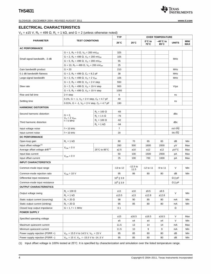
ELECTRICAL CHARACTERISTICSVS = ±15 V, RF = 499 Ω, RL = 1 kΩ, and G = 2 (unless otherwise noted)
TYP OVER TEMPERATUREPARAMETER TEST CONDITIONS 0°C to –40°C to MIN/25°C 25°C UNITS70°C 85°C MAX
AC PERFORMANCE
G = 1, RF = 0 Ω, VO = 200 mVPP 325
G = 2, RF = 499 Ω, VO = 200 mVPP 105Small signal bandwidth, -3 dB MHz
G = 5, RF = 499 Ω, VO = 200 mVPP 55
G = 10, RF = 499 Ω, VO = 200 mVPP 25
Gain bandwidth product G > 20 210 MHz
0.1 dB bandwidth flatness G = 2, RF = 499 Ω, CF = 8.2 pF 38 MHz
Large-signal bandwidth G = 2, RF = 499 Ω, VO = 2 VPP 105 MHz
G = 2, RF = 499 Ω, VO = 2-V step 550
Slew rate G = 2, RF = 499 Ω, VO = 10-V step 900 V/µs
G = 5, RF = 499 Ω, VO = 10-V step 1000
Rise and fall time 2-V step 5 ns
0.1%, G = -1, VO = 2-V step, CF = 4.7 pF 40Settling time ns
0.01%, G = -1, VO = 2-V step, CF = 4.7 pF 190
HARMONIC DISTORTION
RL = 100 Ω -65Second harmonic distortion dBc
G = 2, RL = 1 k Ω -76VO = 2 VPP,
RL = 100 Ω -62f = 5 MHzThird harmonic distortion dBc
RL = 1 kΩ -94
Input voltage noise f > 10 kHz 7 nV/√Hz
Input current noise f > 10 kHz 20 fA/√Hz
DC PERFORMANCE
Open-loop gain RL = 1 kΩ 80 70 65 65 dB Min
Input offset voltage (1) 260 500 1600 2000 µV MaxVCM = 0 V
Average offset voltage drift (1) 25°C to 85°C ±2.5 ±10 ±12 ±12 µV/°C Max
Input bias current 50 100 1500 2000 pA MaxVCM = 0 V
Input offset current 25 100 700 1000 pA Max
INPUT CHARACTERISTICS
-12.5 toCommon-mode input range -13 to 12 -12 to 11 -9 to 11 V Min11.5
Common-mode rejection ratio VCM = 10 V 95 86 80 80 dB Min
Differential input resistance Ω || pF109 || 3.9
Common-mode input resistance Ω || pF109 || 3.9
OUTPUT CHARACTERISTICS
RL = 100 Ω ±11 ±10 ±9.5 ±9.5Output voltage swing V Min
RL = 1 kΩ ±13.5 ±13 ±12.8 ±12.8
Static output current (sourcing) RL = 20 Ω 98 90 85 80 mA Min
Static output current (sinking) RL = 20 Ω 95 85 80 80 mA Min
Closed loop output impedance G = 1, f = 1 MHz 0.1 Ω
POWER SUPPLY
±15 ±16.5 ±16.5 ±16.5 V MaxSpecified operating voltage
±5 ±4 ±4 ±4 V Min
Maximum quiescent current 11.5 13 14 14 mA Max
Minimum quiescent current 11.5 10 9 9 mA Min
Power supply rejection (PSRR +) VS+ = 15.5 V to 14.5 V, VS– = 15 V 95 85 80 80 dB Min
Power supply rejection (PSRR –) VS+ = 15 V, VS– = -15.5 V to -14..5 V 95 85 80 80 dB Min
(1) Input offset voltage is 100% tested at 25°C. It is specified by characterization and simulation over the listed temperature range.
4 Copyright © 2004–2011, Texas Instruments Incorporated
_
+
THS463149.9 Ω
50 Ω Source
+15 V
953 Ω
499 Ω 499 Ω
−15 V
49.9 Ω
Test DataMesurement Point
50 Ω TestEquipment
CF
RFRG
0
1
2
3
4
5
6
7
8
9
10
100 k 1 M 10 M 100 M 1 G
VO = 200 mVPP
G = 2, RF = 499 Ω,RG = 499 Ω
105 MHz
f − Frequency − Hz
Sig
nal G
ain
− dB
CF = 5.6 pF
CF = 0 pF
CF = 8.2 pF
5.6
5.7
5.8
5.9
6
6.1
6.2
6.3
100 k 1 M 10 M 100 M
f − Frequency − Hz
Sig
nal G
ain
− dB CF = 8.2 pF
38 MHz
−10
0
10
20
30
40
50
100 k 1 M 10 M 100 M 1 G
G = 100, RF = 11.3 kΩ, RG = 115 Ω
VO = 200 mVPP
G = 10, RF = 499 Ω,RG = 54.9 Ω
G = 5, RF = 499 Ω,RG = 124 Ω
G = 2, RF = 499 Ω,RG = 499 Ω
G = 1, RF = 0 Ω
105 MHz
f − Frequency − Hz
Sig
nal G
ain
− dB
−5
−4
−3
−2
−1
0
1
2
3
4
5
100 k 1 M 10 M 100 M 1 G
G = −1, RF = 499 Ω,RG = 499 Ω
CF = 2.2 pF
CF = 0 pF
CF = 5.2 pF
VO = 200 mVPP
f − Frequency − Hz
Sig
nal G
ain
− dB
102 MHz
−10
−8
−6
−4
−2
0
2
4
100 k 1 M 10 M 100 M 1 G
THS4631
+15 V
RL
RISO
−15 V0 Ω
50 ΩSource
G = 1,RF = 0 Ω,RL = 1 kΩ
RISO = 50 Ω,CL = 10 pF
RISO = 30 Ω,CL = 56 pF
f − Frequency − Hz
Sig
nal G
ain
− dB
RISO = 20 Ω,CL = 100 pF
CL
0
1
2
3
4
5
6
7
8
100 k 1 M 10 M 100 M 1 G
VO = 0.5 VPP
VO = 2 VPP
f − Frequency − Hz
Sig
nal G
ain
− dB
VO = 5 VPP
105 MHz
THS4631
www.ti.com SLOS451B –DECEMBER 2004–REVISED AUGUST 2011
TYPICAL CHARACTERISTICS (±15 V GRAPHS)TA = 25°C, G = 2, RF = 499 Ω, RL = 1 kΩ, Unless otherwise noted.
SMALL SIGNAL FREQUENCY SMALL SIGNAL FREQUENCYRESPONSE RESPONSE 0.1-dB FLATNESS
Figure 1. Figure 2. Figure 3.
FREQUENCY RESPONSESMALL SIGNAL FREQUENCY LARGE SIGNAL FREQUENCY vs
RESPONSE RESPONSE CAPACiTIVE LOAD
Figure 4. Figure 5. Figure 6.
Copyright © 2004–2011, Texas Instruments Incorporated 5
-100
-95
-90
-85
-80
-75
-70
-65
-60
-55
-50
0 0.5 1 1.5 2 2.5 3 3.5 4
Harm
on
ic D
isto
rtio
n -
dB
VO - Output Voltage Swing - VPP
G = 2,RF = 499 ,W
CF = 8.2 pF,f = 4 MHz
HD3, RL = 100 W
HD2, RL = 1 kW
HD3, RL = 1 kW
HD2, RL = 100 W
−90
−80
−70
−60
−50
−40
−30
1 M 10 M 100 M
2nd
Ord
er H
arm
onic
Dis
tort
ion
− dB
f − Frequency − Hz
Gain = 2RF = 499 Ω,CF = 8.2 pFVO = 2 VPP
RL = 100 Ω
RL = 1 kΩ
-1 10
-100
-90
-80
-70
-60
-50
-40
-30
1 M 10 M 100 M
f - Frequency - Hz
3rd
Ord
er
Ha
rmo
nic
Dis
tort
ion
- d
B
Gain = 2RF = 499 W
CF = 8.2 pFVO = 2 VPP
RL = 100 W
RL = 1 kW
−10
0
10
20
30
40
50
60
70
80
90
1 k 10 k 100 k 1 M 10 M 100 M 1 G
f − Frequency − Hz
Ope
n−Lo
op G
ain
− dB
−200
−175
−150
−125
−100
−75
−50
−25
0
25
50
Pha
se −
0
200
400
600
800
1000
1200
0 2 4 6 8 10 12
VO − Output V oltage − V PP
G = 5,RF = 499 Ω,RG = 124 Ω
SR
− S
lew
Rat
e −
V/
µs
72
73
74
75
76
77
78
79
80
81
82
−40−30−20−10 0 10 20 30 40 50 60 70 80 90
TC − Case Temperature − °C
Ope
n-Lo
op G
ain
− dB
9
9.5
10
10.5
11
11.5
12
0 2 4 6 8 10 12 14 16
TA = 85°C
TA = 25°C
− Q
uies
cent
Cur
rent
− m
AI Q
VS − Supply V oltage − V
TA = −40°C
nV/
Hz
Inpu
t Vol
tage
Noi
se −
1
10
100
10 100 1 k 10 k 100 k
f − Frequency − Hz
0
100
200
300
400
500
600
700
800
−40−30−20−10 0 10 20 30 40 50 60 70 80 90
I IB
− In
put B
ias
Cur
rent
− p
A
TA − Free-Air T emperature − °C
THS4631
SLOS451B –DECEMBER 2004–REVISED AUGUST 2011 www.ti.com
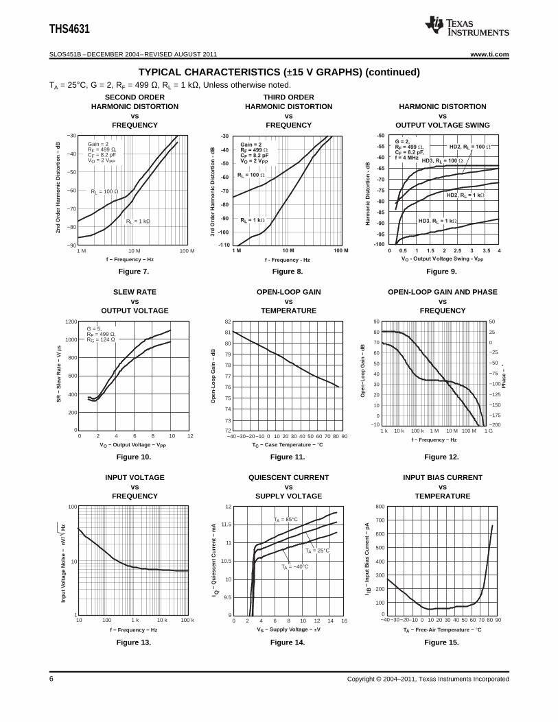
TYPICAL CHARACTERISTICS (±15 V GRAPHS) (continued)TA = 25°C, G = 2, RF = 499 Ω, RL = 1 kΩ, Unless otherwise noted.
SECOND ORDER THIRD ORDERHARMONIC DISTORTION HARMONIC DISTORTION HARMONIC DISTORTION
vs vs vsFREQUENCY FREQUENCY OUTPUT VOLTAGE SWING
Figure 7. Figure 8. Figure 9.
SLEW RATE OPEN-LOOP GAIN OPEN-LOOP GAIN AND PHASEvs vs vs
OUTPUT VOLTAGE TEMPERATURE FREQUENCY
Figure 10. Figure 11. Figure 12.
INPUT VOLTAGE QUIESCENT CURRENT INPUT BIAS CURRENTvs vs vs
FREQUENCY SUPPLY VOLTAGE TEMPERATURE
Figure 13. Figure 14. Figure 15.
6 Copyright © 2004–2011, Texas Instruments Incorporated
−300
−200
−100
0
100
200
300
25 35 45 55 65 75 85
Inpu
t Offs
et V
olta
ge −
TA − Free-Air T emperature − °C
V
D Package
DDA Package
DGN Package
Referred to 25°C
0
25
50
75
100
125
150
175
200
225
250
−40−30−20−10 0 10 20 30 40 50 60 70 80 90
I IO
− In
put O
ffset
Cur
rent
− p
A
TA − Free-Air T emperature − °C
13.2
13.25
13.3
13.35
13.4
13.45
13.5
13.55
−40−30−20−10 0 10 20 30 40 50 60 70 80 90
− O
utpu
t Vol
tage
− |V
|V O
TC − Case Temperature − °C
VO+
VO−−
Out
put V
olta
ge −
mV
VO
−125
−100
−75
−50
−25
0
25
50
75
100
125
0 10 20 30 40 50 60 70 80
t − Time− ns
Gain = 2,CF = 8.2 pF,VI = 100 mVPP,RL = 1 kΩ
−1.2
−1
−0.8
−0.6
−0.4
−0.2
0
0.2
0.4
0.6
0.8
1
1.2
0 10 20 30 40 50 60 70 80
Gain = 2,CF = 8.2 pF,VI = 1 VPP,RL = 1 kΩ
t − Time − ns
− O
utpu
t Vol
tage
− V
VO
84
86
88
90
92
94
96
98
100
−40−30−20−10 0 10 20 30 40 50 60 70 80 90
Sink
Source
I O−
Out
put D
rive
Cur
rent
− |m
A|
TC − Case Temperature − °C
-7
-5
-3
-1
1
3
5
7
0 20 40 60 80 100 120 140 180160
Gain = 5,
R = 499 ,
R = 1 k
F
L
W
W
10 VPP
t - Time - ns
- O
utp
ut
Vo
ltag
e -
VV
O
-12
-8
-4
0
4
8
12
10
6
2
-2
-6
-10
0 20 40 60 80 100 120 140 180160
t - Time - ns
- O
utp
ut
Vo
ltag
e -
VV
O
20 VPP
Gain = 5,
R = 499 ,W
R = 1 kW
F
L
Gain = 2,CF = 8.2 pF,VI = 2 VPP,RL = 1 kΩ
− O
utpu
t Vol
tage
− V
VO
−2.5
−2
−1.5
−1
−0.5
0
0.5
1
1.5
2
2.5
0 25 50 75 100 125 150
t − Time− ns
Gain = 2,CF = 8.2 pF,VI = 2 VPP,RL = 1 kΩ
THS4631
www.ti.com SLOS451B –DECEMBER 2004–REVISED AUGUST 2011
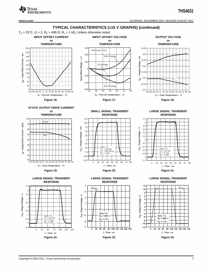
TYPICAL CHARACTERISTICS (±15 V GRAPHS) (continued)TA = 25°C, G = 2, RF = 499 Ω, RL = 1 kΩ, Unless otherwise noted.
INPUT OFFSET CURRENT INPUT OFFSET VOLTAGE OUTPUT VOLTAGEvs vs vs
TEMPERATURE TEMPERATURE TEMPERATURE
Figure 16. Figure 17. Figure 18.
STATIC OUTPUT DRIVE CURRENTvs SMALL SIGNAL TRANSIENT LARGE SIGNAL TRANSIENT
TEMPERATURE RESPONSE RESPONSE
Figure 19. Figure 20. Figure 21.
LARGE SIGNAL TRANSIENT LARGE SIGNAL TRANSIENT LARGE SIGNAL TRANSIENTRESPONSE RESPONSE RESPONSE
Figure 22. Figure 23. Figure 24.
Copyright © 2004–2011, Texas Instruments Incorporated 7
− O
utpu
t Vol
tage
− V
VO
t − Time − ns
−3
−2.5
−2
−1.5
−1
−0.5
0
0.5
1
1.5
2
2.5
3
0 5 10 15 20 25 30 35 40
Rising
Falling
G = −1,CF = 4.7 pF
− O
utpu
t Vol
tage
− V
VO
t − Time − ns
−1.5
−1.25
−1
−0.75
−0.5
−0.25
0
0.25
0.5
0.75
1
1.25
1.5
0 5 10 15 20 25 30 35 40
Rising
Falling
G = −1,CF = 4.7 pF
−20
−15
−10
−5
0
5
10
15
20
0 0.1 0.2 0.3 0.4 0.5 0.6 0.7 0.8 0.9 1−4
−3
−2
−1
0
1
2
3
4Gain = 5,RF = 499 Ω,RG = 124 Ω
t − Time − s
− O
utpu
t Vol
tage
− V
VO
Input
Output − In
put V
olta
ge −
VV
I
−20
−15
−10
−5
0
5
10
15
20
−0.05 0 0.05 0.1 0.15 0.2 0.25 0.3 0.35−4
−3
−2
−1
0
1
2
3
4
Gain = 5,RF = 499 Ω,RG = 124 Ω
t − Time − s
− O
utpu
t Vol
tage
− V
VO
Input
Output
− In
put V
olta
ge −
VV
I
0
10
20
30
40
50
60
70
80
90
100
−15 −10 −5 0 5 10 15
VICR − Input Common-Mode Range − V
CM
RR
− C
omm
on-M
ode
Rej
ectio
n R
atio
− d
B
0
10
20
30
40
70
80
90
100
10 k 100 k 1 M 10 M 100 M
f − Frequency − Hz
Rej
ectio
n R
atio
− d
B
50
60
CMRR
PSRR+
PSRR−
0.01
0.1
1
10
100
100 k 1 M 10 M 100 M 1 G
f − Frequency − Hz
− O
utpu
t Im
peda
nce
−Z
oΩ
THS4631
SLOS451B –DECEMBER 2004–REVISED AUGUST 2011 www.ti.com
TYPICAL CHARACTERISTICS (±15 V GRAPHS) (continued)TA = 25°C, G = 2, RF = 499 Ω, RL = 1 kΩ, Unless otherwise noted.
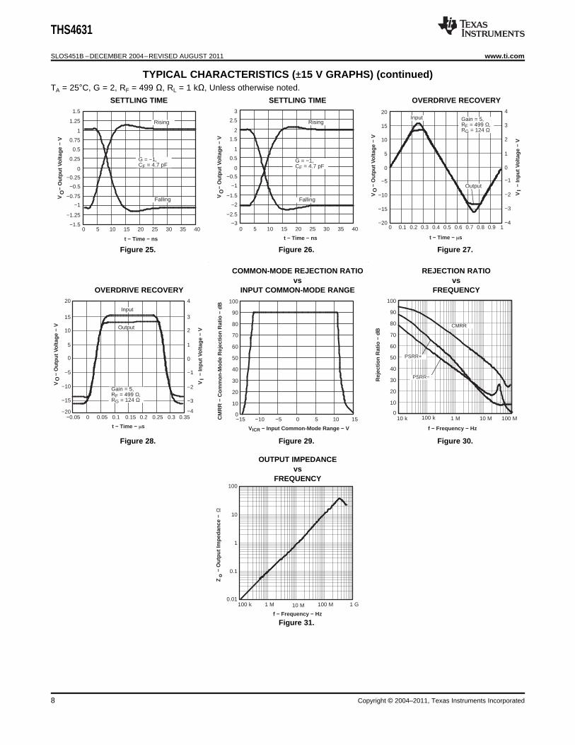
SETTLING TIME SETTLING TIME OVERDRIVE RECOVERY
Figure 25. Figure 26. Figure 27.
COMMON-MODE REJECTION RATIO REJECTION RATIOvs vs
OVERDRIVE RECOVERY INPUT COMMON-MODE RANGE FREQUENCY
Figure 28. Figure 29. Figure 30.
OUTPUT IMPEDANCEvs
FREQUENCY
Figure 31.
8 Copyright © 2004–2011, Texas Instruments Incorporated
_
+
RF
CF
λ
−V(Bias)
RL
Photodiode Circuit
THS4631
www.ti.com SLOS451B –DECEMBER 2004–REVISED AUGUST 2011
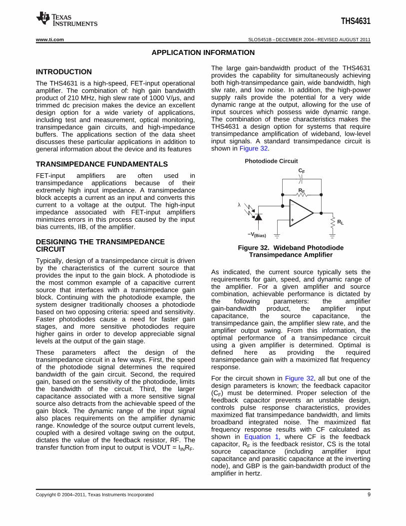
APPLICATION INFORMATION
The large gain-bandwidth product of the THS4631INTRODUCTION provides the capability for simultaneously achievingboth high-transimpedance gain, wide bandwidth, highThe THS4631 is a high-speed, FET-input operationalslw rate, and low noise. In addition, the high-poweramplifier. The combination of: high gain bandwidthsupply rails provide the potential for a very wideproduct of 210 MHz, high slew rate of 1000 V/µs, anddynamic range at the output, allowing for the use oftrimmed dc precision makes the device an excellentinput sources which possess wide dynamic range.design option for a wide variety of applications,The combination of these characteristics makes theincluding test and measurement, optical monitoring,THS4631 a design option for systems that requiretransimpedance gain circuits, and high-impedancetransimpedance amplification of wideband, low-levelbuffers. The applications section of the data sheetinput signals. A standard transimpedance circuit isdiscusses these particular applications in addition toshown in Figure 32.general information about the device and its features
TRANSIMPEDANCE FUNDAMENTALS
FET-input amplifiers are often used intransimpedance applications because of theirextremely high input impedance. A transimpedanceblock accepts a current as an input and converts thiscurrent to a voltage at the output. The high-inputimpedance associated with FET-input amplifiersminimizes errors in this process caused by the inputbias currents, IIB, of the amplifier.
DESIGNING THE TRANSIMPEDANCEFigure 32. Wideband PhotodiodeCIRCUIT
Transimpedance AmplifierTypically, design of a transimpedance circuit is drivenby the characteristics of the current source that
As indicated, the current source typically sets theprovides the input to the gain block. A photodiode isrequirements for gain, speed, and dynamic range ofthe most common example of a capacitive currentthe amplifier. For a given amplifier and sourcesource that interfaces with a transimpedance gaincombination, achievable performance is dictated byblock. Continuing with the photodiode example, thethe following parameters: the amplifiersystem designer traditionally chooses a photodiodegain-bandwidth product, the amplifier inputbased on two opposing criteria: speed and sensitivity.capacitance, the source capacitance, theFaster photodiodes cause a need for faster gaintransimpedance gain, the amplifier slew rate, and thestages, and more sensitive photodiodes requireamplifier output swing. From this information, thehigher gains in order to develop appreciable signaloptimal performance of a transimpedance circuitlevels at the output of the gain stage.using a given amplifier is determined. Optimal is
These parameters affect the design of the defined here as providing the requiredtransimpedance circuit in a few ways. First, the speed transimpedance gain with a maximized flat frequencyof the photodiode signal determines the required response.bandwidth of the gain circuit. Second, the required
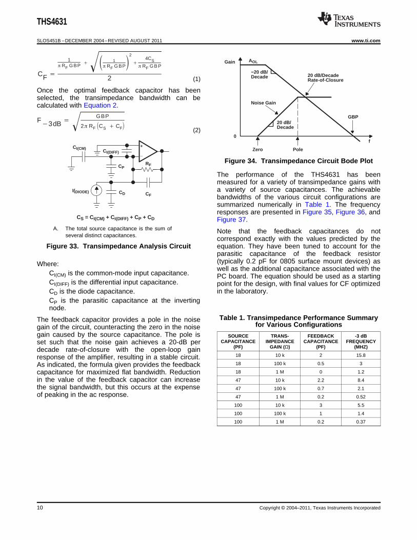
For the circuit shown in Figure 32, all but one of thegain, based on the sensitivity of the photodiode, limitsdesign parameters is known; the feedback capacitorthe bandwidth of the circuit. Third, the larger(CF) must be determined. Proper selection of thecapacitance associated with a more sensitive signalfeedback capacitor prevents an unstable design,source also detracts from the achievable speed of thecontrols pulse response characteristics, providesgain block. The dynamic range of the input signalmaximized flat transimpedance bandwidth, and limitsalso places requirements on the amplifier dynamicbroadband integrated noise. The maximized flatrange. Knowledge of the source output current levels,frequency response results with CF calculated ascoupled with a desired voltage swing on the output,shown in Equation 1, where CF is the feedbackdictates the value of the feedback resistor, RF. Thecapacitor, RF is the feedback resistor, CS is the totaltransfer function from input to output is VOUT = IINRF.source capacitance (including amplifier inputcapacitance and parasitic capacitance at the invertingnode), and GBP is the gain-bandwidth product of theamplifier in hertz.
Copyright © 2004–2011, Texas Instruments Incorporated 9
CF
1 RF G BP
1 RF G BP
2
4CS
RF G B P
2
F3dB GBP
2 RFCS CF
Gain AOL
20 dB/DecadeRate-of-Closure
GBP20 dB/Decade
Noise Gain
−20 dB/Decade
f
PoleZero
0
_
+CI(DIFF)
RF
CF
CP
CDI(DIODE)
CI(CM)
CS = CI(CM) + CI(DIFF) + CP + CD
THS4631
SLOS451B –DECEMBER 2004–REVISED AUGUST 2011 www.ti.com
(1)
Once the optimal feedback capacitor has beenselected, the transimpedance bandwidth can becalculated with Equation 2.
(2)
Figure 34. Transimpedance Circuit Bode Plot
The performance of the THS4631 has beenmeasured for a variety of transimpedance gains witha variety of source capacitances. The achievablebandwidths of the various circuit configurations aresummarized numerically in Table 1. The frequencyresponses are presented in Figure 35, Figure 36, andFigure 37.
A. The total source capacitance is the sum of Note that the feedback capacitances do notseveral distinct capacitances. correspond exactly with the values predicted by the
Figure 33. Transimpedance Analysis Circuit equation. They have been tuned to account for theparasitic capacitance of the feedback resistor(typically 0.2 pF for 0805 surface mount devices) asWhere:well as the additional capacitance associated with the
CI(CM) is the common-mode input capacitance. PC board. The equation should be used as a startingCI(DIFF) is the differential input capacitance. point for the design, with final values for CF optimized
in the laboratory.CD is the diode capacitance.CP is the parasitic capacitance at the invertingnode.
Table 1. Transimpedance Performance SummaryThe feedback capacitor provides a pole in the noisefor Various Configurationsgain of the circuit, counteracting the zero in the noise
gain caused by the source capacitance. The pole is SOURCE TRANS- FEEDBACK -3 dBCAPACITANCE IMPEDANCE CAPACITANCE FREQUENCYset such that the noise gain achieves a 20-dB per
(PF) GAIN (Ω) (PF) (MHZ)decade rate-of-closure with the open-loop gain18 10 k 2 15.8response of the amplifier, resulting in a stable circuit.18 100 k 0.5 3As indicated, the formula given provides the feedback18 1 M 0 1.2capacitance for maximized flat bandwidth. Reduction
in the value of the feedback capacitor can increase 47 10 k 2.2 8.4
the signal bandwidth, but this occurs at the expense 47 100 k 0.7 2.1of peaking in the ac response. 47 1 M 0.2 0.52
100 10 k 3 5.5
100 100 k 1 1.4
100 1 M 0.2 0.37
10 Copyright © 2004–2011, Texas Instruments Incorporated
65
70
75
80
85
10 k 100 k 1 M 10 M 1 G
f − Frequency − Hz
Tran
sim
peda
nce
Gai
n −
dB
VS = ±15 VRL = 1 kRF = 10 k
CS = 100 PFCF = 3 PF
CS = 18 PFCF = 2 PF
CS = 47 PFCF = 2.2 PF
50 50
RS
VS
C1
C2
IONetwork Analizer
IOVS
(s) 1
2RS1
C1C2
(Above the Pole Frequency)
IOVS
(s)
s
2RS 1C1C2
s 12 RS
C1C285
90
95
100
105
10 k 100 k 1 M 10 M 1 G
f − Frequency − Hz
Tran
sim
peda
nce
Gai
n −
dB
VS = ±15 VRL = 1 kRF = 100 k
CS = 47 PFCF = 0.7 PF
CS = 100 PFCF = 1 PF
CS = 18 PFCF = 0.5 PF
12 RS (C1 C2)
1
2 RS1 C1
C2
95
100
110
120
10 k 100 k 1 M 10 M
f − Frequency − Hz
Tran
sim
peda
nce
Gai
n −
dB
125
VS = ±15 VRL = 1 kRF = 1 M
115
105
CS = 18 PFCF = 0 PF
CS = 47 PFCF = 0.2 PF
CS = 100 PFCF = 0.2 PF
ZO(s) C1 C2C1 C2
s 12RS
C1C2
ss 12 RS C1
ZO 1
sC2
THS4631
www.ti.com SLOS451B –DECEMBER 2004–REVISED AUGUST 2011
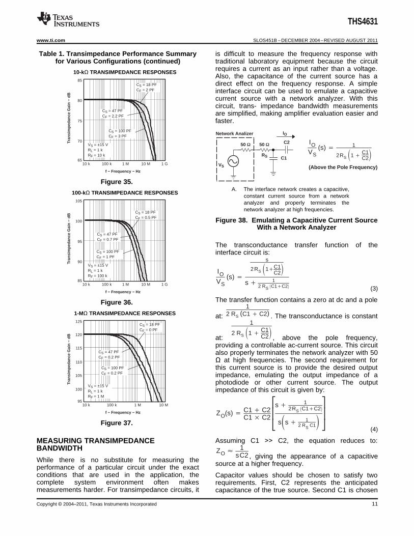
Table 1. Transimpedance Performance Summary is difficult to measure the frequency response withfor Various Configurations (continued) traditional laboratory equipment because the circuit
requires a current as an input rather than a voltage.10-kΩ TRANSIMPEDANCE RESPONSESAlso, the capacitance of the current source has adirect effect on the frequency response. A simpleinterface circuit can be used to emulate a capacitivecurrent source with a network analyzer. With thiscircuit, trans- impedance bandwidth measurementsare simplified, making amplifier evaluation easier andfaster.
Figure 35.A. The interface network creates a capacitive,
100-kΩ TRANSIMPEDANCE RESPONSESconstant current source from a networkanalyzer and properly terminates thenetwork analyzer at high frequencies.
Figure 38. Emulating a Capacitive Current SourceWith a Network Analyzer
The transconductance transfer function of theinterface circuit is:
(3)
The transfer function contains a zero at dc and a poleFigure 36.
1-MΩ TRANSIMPEDANCE RESPONSES at: . The transconductance is constant
at: , above the pole frequency,providing a controllable ac-current source. This circuitalso properly terminates the network analyzer with 50Ω at high frequencies. The second requirement forthis current source is to provide the desired outputimpedance, emulating the output impedance of aphotodiode or other current source. The outputimpedance of this circuit is given by:
Figure 37.(4)
Assuming C1 >> C2, the equation reduces to:MEASURING TRANSIMPEDANCEBANDWIDTH
, giving the appearance of a capacitiveWhile there is no substitute for measuring the source at a higher frequency.performance of a particular circuit under the exactconditions that are used in the application, the Capacitor values should be chosen to satisfy twocomplete system environment often makes requirements. First, C2 represents the anticipatedmeasurements harder. For transimpedance circuits, it capacitance of the true source. Second C1 is chosen
Copyright © 2004–2011, Texas Instruments Incorporated 11
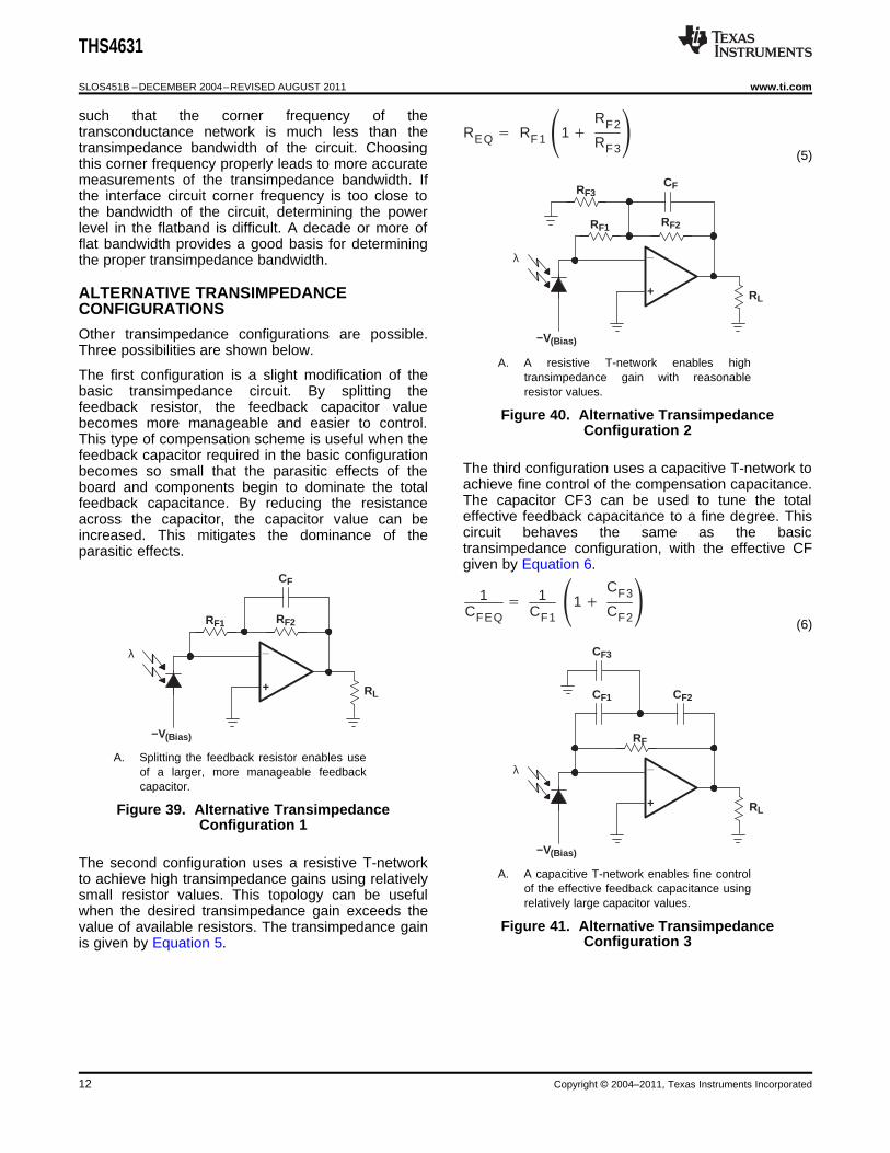
REQ RF1 1 RF2
RF3
_
+
RF2
CF
λ
−V(Bias)
RL
RF1
RF3
1CFEQ
1CF11
CF3
CF2
_
+
RF2
CF
λ
−V(Bias)
RL
RF1
_
+
RF
CF2
λ
−V(Bias)
RL
CF1
CF3
THS4631
SLOS451B –DECEMBER 2004–REVISED AUGUST 2011 www.ti.com
such that the corner frequency of thetransconductance network is much less than thetransimpedance bandwidth of the circuit. Choosing (5)this corner frequency properly leads to more accuratemeasurements of the transimpedance bandwidth. Ifthe interface circuit corner frequency is too close tothe bandwidth of the circuit, determining the powerlevel in the flatband is difficult. A decade or more offlat bandwidth provides a good basis for determiningthe proper transimpedance bandwidth.
ALTERNATIVE TRANSIMPEDANCECONFIGURATIONS
Other transimpedance configurations are possible.Three possibilities are shown below.
A. A resistive T-network enables highThe first configuration is a slight modification of the transimpedance gain with reasonablebasic transimpedance circuit. By splitting the resistor values.feedback resistor, the feedback capacitor value Figure 40. Alternative Transimpedancebecomes more manageable and easier to control. Configuration 2This type of compensation scheme is useful when thefeedback capacitor required in the basic configuration
The third configuration uses a capacitive T-network tobecomes so small that the parasitic effects of theachieve fine control of the compensation capacitance.board and components begin to dominate the totalThe capacitor CF3 can be used to tune the totalfeedback capacitance. By reducing the resistanceeffective feedback capacitance to a fine degree. Thisacross the capacitor, the capacitor value can becircuit behaves the same as the basicincreased. This mitigates the dominance of thetransimpedance configuration, with the effective CFparasitic effects.given by Equation 6.
(6)
A. Splitting the feedback resistor enables useof a larger, more manageable feedbackcapacitor.
Figure 39. Alternative TransimpedanceConfiguration 1
The second configuration uses a resistive T-networkA. A capacitive T-network enables fine controlto achieve high transimpedance gains using relatively
of the effective feedback capacitance usingsmall resistor values. This topology can be usefulrelatively large capacitor values.
when the desired transimpedance gain exceeds theFigure 41. Alternative Transimpedancevalue of available resistors. The transimpedance gain
Configuration 3is given by Equation 5.
12 Copyright © 2004–2011, Texas Instruments Incorporated
_
+
Rf
4kT = 1.6E−20Jat 290K
IBNEO
ERF
RS
ERS
IBIRg
ENI
4kTRS
4kTRg
4kTRf
EO E 2NI IBNRS
2 4kTRSNG2 IBIRf2 4kTRfNG
EN E 2NI IBNRS
2 4kTRS IBIR f
NG
2
4kTR f
NG
THS4631
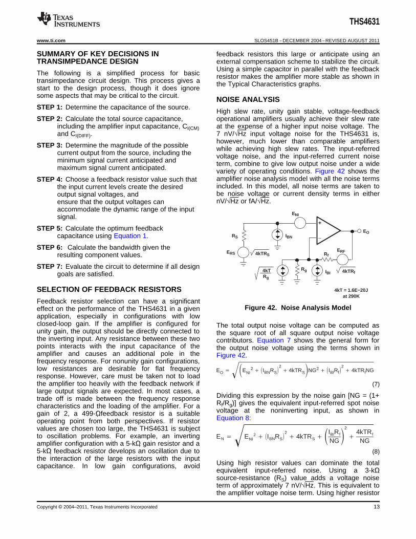
www.ti.com SLOS451B –DECEMBER 2004–REVISED AUGUST 2011
SUMMARY OF KEY DECISIONS IN feedback resistors this large or anticipate using anTRANSIMPEDANCE DESIGN external compensation scheme to stabilize the circuit.
Using a simple capacitor in parallel with the feedbackThe following is a simplified process for basic resistor makes the amplifier more stable as shown intransimpedance circuit design. This process gives a the Typical Characteristics graphs.start to the design process, though it does ignoresome aspects that may be critical to the circuit. NOISE ANALYSISSTEP 1: Determine the capacitance of the source.
High slew rate, unity gain stable, voltage-feedbackSTEP 2: Calculate the total source capacitance, operational amplifiers usually achieve their slew rate
including the amplifier input capacitance, CI(CM) at the expense of a higher input noise voltage. Theand CI(DIFF). 7 nV/√Hz input voltage noise for the THS4631 is,
however, much lower than comparable amplifiersSTEP 3: Determine the magnitude of the possible while achieving high slew rates. The input-referred
current output from the source, including the voltage noise, and the input-referred current noiseminimum signal current anticipated and term, combine to give low output noise under a widemaximum signal current anticipated. variety of operating conditions. Figure 42 shows the
amplifier noise analysis model with all the noise termsSTEP 4: Choose a feedback resistor value such thatincluded. In this model, all noise terms are taken tothe input current levels create the desiredbe noise voltage or current density terms in eitheroutput signal voltages, andnV/√Hz or fA/√Hz.ensure that the output voltages can
accommodate the dynamic range of the inputsignal.
STEP 5: Calculate the optimum feedbackcapacitance using Equation 1.
STEP 6: Calculate the bandwidth given theresulting component values.
STEP 7: Evaluate the circuit to determine if all designgoals are satisfied.
SELECTION OF FEEDBACK RESISTORS
Feedback resistor selection can have a significantFigure 42. Noise Analysis Modeleffect on the performance of the THS4631 in a given
application, especially in configurations with lowclosed-loop gain. If the amplifier is configured for The total output noise voltage can be computed asunity gain, the output should be directly connected to the square root of all square output noise voltagethe inverting input. Any resistance between these two contributors. Equation 7 shows the general form forpoints interacts with the input capacitance of the the output noise voltage using the terms shown inamplifier and causes an additional pole in the Figure 42.frequency response. For nonunity gain configurations,low resistances are desirable for flat frequencyresponse. However, care must be taken not to loadthe amplifier too heavily with the feedback network if (7)large output signals are expected. In most cases, a
Dividing this expression by the noise gain [NG = (1+trade off is made between the frequency responseRf/Rg)] gives the equivalent input-referred spot noisecharacteristics and the loading of the amplifier. For avoltage at the noninverting input, as shown ingain of 2, a 499-Ωfeedback resistor is a suitableEquation 8:operating point from both perspectives. If resistor
values are chosen too large, the THS4631 is subjectto oscillation problems. For example, an invertingamplifier configuration with a 5-kΩ gain resistor and a5-kΩ feedback resistor develops an oscillation due to (8)the interaction of the large resistors with the input
Using high resistor values can dominate the totalcapacitance. In low gain configurations, avoidequivalent input-referred noise. Using a 3-kΩsource-resistance (RS) value adds a voltage noiseterm of approximately 7 nV/√Hz. This is equivalent tothe amplifier voltage noise term. Using higher resistor
Copyright © 2004–2011, Texas Instruments Incorporated 13
THS4631
SLOS451B –DECEMBER 2004–REVISED AUGUST 2011 www.ti.com
values dominate the noise of the system. Although performance of the THS4631. Resistors should bethe THS4631 JFET input stage is ideal for a very low reactance type. Surface-mounthigh-source impedance because of the low-bias resistors work best and allow a tighter overallcurrents, the system noise and bandwidth is limited layout. Again, keep their leads and PC boardby a high-source (RS) impedance. trace length as short as possible. Never use
wirebound type resistors in a high frequencyapplication. Since the output pin and invertingSLEW RATE PERFORMANCE WITH VARYINGinput pins are the most sensitive to parasiticINPUT STEP AMPLITUDE AND RISE/FALLcapacitance, always position the feedback andTIMEseries output resistors, if any, as close as possible
Some FET input amplifiers exhibit the peculiar to the inverting input pins and output pins. Otherbehavior of having a larger slew rate when presented network components, such as input terminationwith smaller input voltage steps and slower edge resistors, should be placed close to therates due to a change in bias conditions in the input gain-setting resistors. Even with a low parasiticstage of the amplifier under these circumstances. capacitance shunting the external resistors,This phenomena is most commonly seen when FET excessively high resistor values can createinput amplifiers are used as voltage followers. As this significant time constants that can degradebehavior is typically undesirable, the THS4631 has performance. Good axial metal-film orbeen designed to avoid these issues. Larger surface-mount resistors have approximately 0.2amplitudes lead to higher slew rates, as would be pF in shunt with the resistor. For resistor values >anticipated, and fast edges do not degrade the slew 2.0 kΩ, this parasitic capacitance can add a polerate of the device. The high slew rate of the THS4631 and/or a zero that can effect circuit operation.allows improved SFDR and THD performance, Keep resistor values as low as possible,especially noticeable above 5 MHz. consistent with load driving considerations.
• Connections to other wideband devices on thePRINTED-CIRCUIT BOARD LAYOUT board may be made with short direct traces orTECHNIQUES FOR OPTIMAL through onboard transmission lines. For shortPERFORMANCE connections, consider the trace and the input tothe next device as a lumped capacitive load.Achieving optimum performance with high frequencyRelatively wide traces (50 mils to 100 mils) shouldamplifier-like devices in the THS4631 requires carefulbe used, preferably with ground and power planesattention to board layout parasitic and externalopened up around them. Estimate the totalcomponent types.capacitive load and determine if isolation resistors
Recommendations that optimize performance include: on the outputs are necessary. Low parasitic• Minimize parasitic capacitance to any ac ground capacitive loads (< 4 pF) may not need an RS
for all of the signal I/O pins. Parasitic capacitance since the THS4631 is nominally compensated toon the output and input pins can cause instability. operate with a 2-pF parasitic load. Higher parasiticTo reduce unwanted capacitance, a window capacitive loads without an RS are allowed as thearound the signal I/O pins should be opened in all signal gain increases (increasing the unloadedof the ground and power planes around those phase margin). If a long trace is required, and thepins. Otherwise, ground and power planes should 6-dB signal loss intrinsic to a doubly-terminatedbe unbroken elsewhere on the board. transmission line is acceptable, implement a
matched impedance transmission line using• Minimize the distance (< 0.25”) from the powermicrostrip or stripline techniques (consult an ECLsupply pins to high frequency 0.1-µF and 100-pFdesign handbook for microstrip and stripline layoutde-coupling capacitors. At the device pins, thetechniques). Aground and power plane layout should not be in50-Ω environment is not necessary onboard, andclose proximity to the signal I/O pins. Avoidin fact, a higher impedance environment improvesnarrow power and ground traces to minimizedistortion as shown in the distortion versus loadinductance between the pins and the de-couplingplots. With a characteristic board trace impedancecapacitors. The power supply connections shouldbased on board material and trace dimensions, aalways be de-coupled with these capacitors.matching series resistor into the trace from theLarger (6.8 µF or more) tantalum de-couplingoutput of the THS4631 is used as well as acapacitors, effective at lower frequency, shouldterminating shunt resistor at the input of thealso be used on the main supply pins. These maydestination device. Remember also that thebe placed somewhat farther from the device andterminating impedance is the parallel combinationmay be shared among several devices in theof the shunt resistor and the input impedance ofsame area of the PC board.the destination device: this total effective• Careful selection and placement of externalimpedance should be set to match the tracecomponents preserve the high frequency
14 Copyright © 2004–2011, Texas Instruments Incorporated
0.060
0.040
0.075 0.025
0.205
0.010vias
Pin 1
Top View
0.017
0.035
0.0940.030
0.013
0.140
0.060
0.060
0.010vias
Top View
0.035 0.080
0.050 0.176
0.030
0.026
0.0100.035
0.100
0.300
Pin 1
All Units in Inches
DIE
Side View (a)
DIE
End View (b)
ThermalPad
Bottom View (c)
THS4631
www.ti.com SLOS451B –DECEMBER 2004–REVISED AUGUST 2011
impedance. If the 6-dB attenuation of a doublyterminated transmission line is unacceptable, along trace can be series-terminated at the sourceend only. Treat the trace as a capacitive load inthis case. This does not preserve signal integrityor a doubly-terminated line. If the input impedanceof the destination device is low, there is somesignal attenuation due to the voltage dividerformed by the series output into the terminatingimpedance.
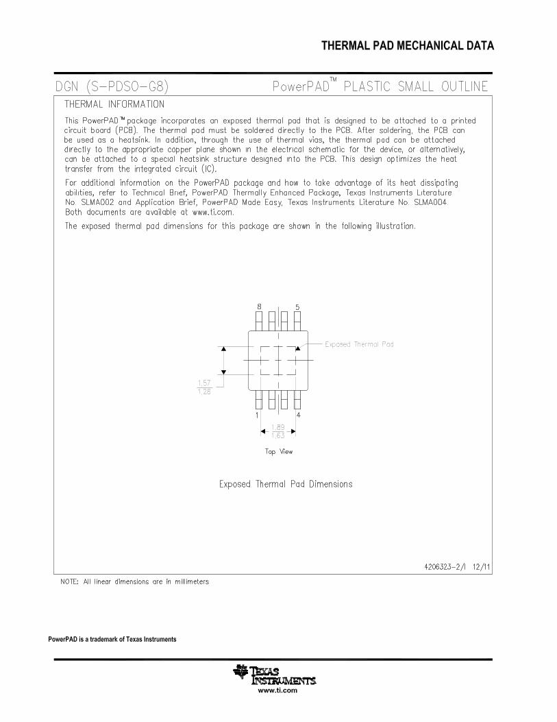
• Socketing a high-speed part like the THS4631 isnot recommended. The additional lead length andpin-to-pin capacitance introduced by the socketcreates a troublesome parasitic network whichmakes it almost impossible to achieve a smooth,stable frequency response. Best results areobtained by soldering the THS4631 part directlyonto the board. Figure 44. DGN PowerPAD PCB Etch and Via
PatternPowerPAD DESIGN CONSIDERATIONS
The THS4631 is available in a thermally-enhancedPowerPAD family of packages. These packages areconstructed using a downset leadframe upon whichthe die is mounted [see Figure 43 (a) and Figure 43(b)]. This arrangement results in the lead frame beingexposed as a thermal pad on the underside of thepackage [see Figure 43 (c)]. Because this thermalpad has direct thermal contact with the die, excellentthermal performance can be achieved by providing agood thermal path away from the thermal pad
The PowerPAD package allows for both assemblyand thermal management in one manufacturingoperation. During the surface-mount solder operation(when the leads are being soldered), the thermal padcan also be soldered to a copper area underneath thepackage. Through the use of thermal paths within thiscopper area, heat can be conducted away from thepackage into either a ground plane or other heat
Figure 45. DDA PowerPAD PCB Etch and Viadissipating device.Pattern
The PowerPAD package represents a breakthroughin combining the small area and ease of assembly ofsurface mount with the mechanical methods of PowerPAD PCB LAYOUT CONSIDERATIONSheatsinking. 1. PCB with a top side etch pattern is shown in
Figure 44 and Figure 45. There should be etchfor the leads and for the thermal pad.
2. Place the recommended number of holes in thearea of the thermal pad. These holes should be10 mils in diameter. Keep them small so thatsolder wicking through the holes is not a problemduring reflow.
3. Additional vias may be placed anywhere alongFigure 43. Views of Thermally Enhanced Packagethe thermal plane outside of the thermal padarea. This helps dissipate the heat generated by
Although there are many ways to properly heatsink the THS4631 IC. These additional vias may bethe PowerPAD package, the following steps illustrate larger than the 10-mil diameter vias directly underthe recommended approach. the thermal pad. They can be larger because
they are not in the thermal pad area to be
Copyright © 2004–2011, Texas Instruments Incorporated 15
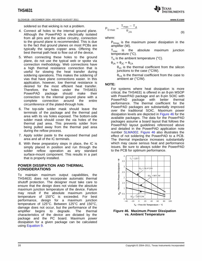
PD max Tmax TA
JA
4
3.5
3
2.5
2
1.5
1
0.5
0−40 −20 0 20 40 60 80 100
− M
axim
um P
ower
Dis
sipa
tion
− W
P D
TA − Free-Air T emperature − °C
θJA = 58.4°C/W
θJA = 98°C/W
θJA = 158°C/W
TJ = 125°C
THS4631
SLOS451B –DECEMBER 2004–REVISED AUGUST 2011 www.ti.com
soldered so that wicking is not a problem.4. Connect all holes to the internal ground plane. (9)
Although the PowerPAD is electrically isolatedwhere:from all pins and the active circuitry, connection
to the ground plane is recommended. This is due PDmax is the maximum power dissipation in theto the fact that ground planes on most PCBs are amplifier (W).typically the targets copper area. Offering the Tmax is the absolute maximum junctionbest thermal path heat to flow out of the device. temperature (°C).
5. When connecting these holes to the ground TA is the ambient temperature (°C).plane, do not use the typical web or spoke via θJA = θJC + θCAconnection methodology. Web connections have
θJC is the thermal coefficient from the silicona high thermal resistance connection that isjunctions to the case (°C/W).useful for slowing the heat transfer duringθCA is the thermal coefficient from the case tosoldering operations. This makes the soldering ofambient air (°C/W).vias that have plane connections easier. In this
application, however, low thermal resistance is NOTE:desired for the most efficient heat transfer.For systems where heat dissipation is moreTherefore, the holes under the THS4631critical, the THS4631 is offered in an 8-pin MSOPPowerPAD package should make theirwith PowerPAD package and an 8-pin SOIC withconnection to the internal ground plane with aPowerPAD package with better thermalcomplete connection around the entireperformance. The thermal coefficient for thecircumference of the plated-through hole.PowerPAD packages are substantially improved
6. The top-side solder mask should leave the over the traditional SOIC. Maximum powerterminals of the package and the thermal pad dissipation levels are depicted in Figure 46 for thearea with its via holes exposed. The bottom-side available packages. The data for the PowerPADsolder mask should cover the via holes of the packages assume a board layout that follows thethermal pad area. This prevents solder from PowerPAD layout guidelines referenced abovebeing pulled away from the thermal pad area and detailed in the PowerPAD application noteduring the reflow process. number SLMA002. Figure 46 also illustrates the
7. Apply solder paste to the exposed thermal pad effect of not soldering the PowerPAD to a PCB.area and all of the IC terminals. The thermal impedance increases substantially
which may cause serious heat and performance8. With these preparatory steps in place, the IC isissues. Be sure to always solder the PowerPADsimply placed in position and run through theto the PCB for optimum performance.solder reflow operation as any standard
surface-mount component. This results in a partthat is properly installed.
POWER DISSIPATION AND THERMALCONSIDERATIONS
To maintain maximum output capabilities, theTHS4631 does not incorporate automatic thermalshutoff protection. The designer must take care toensure that the design does not violate the absolutemaximum junction temperature of the device. Failuremay result if the absolute maximum junctiontemperature of 150°C is exceeded. For bestperformance, design for a maximum junctiontemperature of 125°C. Between 125°C and 150°C,damage does not occur, but the performance of the
Figure 46. Maximum Power Dissipationamplifier begins to degrade. The thermalvs. Ambient Temperaturecharacteristics of the device are dictated by the
package and the PC board. Maximum powerdissipation for a given package can be calculatedusing Equation 9.
16 Copyright © 2004–2011, Texas Instruments Incorporated
THS4631
www.ti.com SLOS451B –DECEMBER 2004–REVISED AUGUST 2011
Results are with no air flow and PCB size = 3" x 3 "θJA = 58.4°C/W for the 8-pin MSOP withPowerPAD (DGN).θJA = 98°C/W for the 8-pin SOIC high-K test PCB(D).θJA = 158°C/W for the 8-pin MSOP withPowerPAD, without solder.
When determining whether or not the device satisfiesthe maximum power dissipation requirement, it isimportant to not only consider quiescent powerdissipation, but also dynamic power dissipation. Oftentimes, this is difficult to quantify because the signalpattern is inconsistent, but an estimate of the RMSpower dissipation can provide visibility into a possibleproblem
DESIGN TOOLS EVALUATION FIXTURE,SPICE MODELS, AND APPLICATIONSSUPPORT
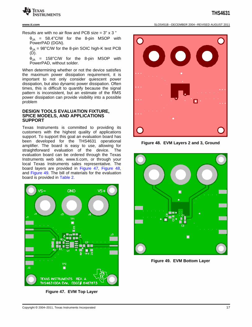
Texas Instruments is committed to providing itscustomers with the highest quality of applicationssupport. To support this goal an evaluation board hasbeen developed for the THS4631 operational Figure 48. EVM Layers 2 and 3, Groundamplifier. The board is easy to use, allowing forstraightforward evaluation of the device. Theevaluation board can be ordered through the TexasInstruments web site, www.ti.com, or through yourlocal Texas Instruments sales representative. Theboard layers are provided in Figure 47, Figure 48,and Figure 49. The bill of materials for the evaluationboard is provided in Table 2.
Figure 49. EVM Bottom Layer
Figure 47. EVM Top Layer
Copyright © 2004–2011, Texas Instruments Incorporated 17
THS4631
SLOS451B –DECEMBER 2004–REVISED AUGUST 2011 www.ti.com
BILL OF MATERIALS
Table 2. THS4631DDA EVM
SMD REFERENCE PCB MANUFACTURER'SITEM DESCRIPTION SIZE DESIGNATOR QUANTITY PART NUMBER (1)
1 CAP, 2.2 µF, CERAMIC, X5R, 25 V 1206 C3, C6 2 (AVX) 12063D225KAT2A
4 CAP, 0.1µF, CERAMIC, X7R, 50 V 0805 C1, C2 2 (AVX) 08055C104KAT2A
OPEN 0805 R4, Z4, Z6 3
6 RESISTOR, 0 OHM, 1/8 W 0805 Z2 1 (KOA) RK73Z2ATTD
7 RESISTOR, 499 OHM, 1/8 W, 1% 0805 R3, Z5 2 (KOA) RK73H2ATTD4990F
8 OPEN 1206 R8, Z9 2
9 RESISTOR, 0 OHM, 1/4 W 1206 R1 1 (KOA) RK73Z2BLTD
10 RESISTOR, 49.9 OHM, 1/4 W, 1% 1206 R2 1 (KOA) RK73H2BLTD49R9F
11 RESISTOR, 953 OHM, 1/4 W, 1% 1206 Z3 1 (KOA) RK73H2BLTD9530F
13 CONNECTOR, SMA PCB JACK J1, J2, J3 3 (JOHNSON) 142-0701-801
JACK, BANANA RECEPTANCE, 0.25"14 J4, J5, J6 3 (SPC) 813DIA. HOLE
15 TEST POINT, BLACK TP1, TP2 2 (KEYSTONE) 5001
TEST POINT, RED TP3 1 (KEYSTONE) 5000
16 STANDOFF, 4-40 HEX, 0.625" LENGTH 4 (KEYSTONE) 1808
17 SCREW, PHILLIPS, 4-40, .250" 4 SHR-0440-016-SN
18 IC, THS4631 U1 1 (TI) THS4631DDA
19 BOARD, PRINTED CIRCUIT 1 (TI) EDGE # 6467873 Rev.A
(1) The manufacturer's part numbers are used for test purposes only.
EVM
Computer simulation of circuit performance using SPICE is often useful when analyzing the performance ofanalog circuits and systems. This is particularly true for video and RF-amplifier circuits where parasiticcapacitance and inductance can have a major effect on circuit performance. A SPICE model for the THS4631 isavailable through either the Texas Instruments web site (www.ti.com). These models help in predictingsmall-signal ac and transient performance under a wide variety of operating conditions. They are not intended tomodel the distortion characteristics of the amplifier, nor do they attempt to distinguish between the package typesin their small-signal ac performance. Detailed information about what is and is not modeled is contained in themodel file itself.
18 Copyright © 2004–2011, Texas Instruments Incorporated
THS4631
www.ti.com SLOS451B –DECEMBER 2004–REVISED AUGUST 2011
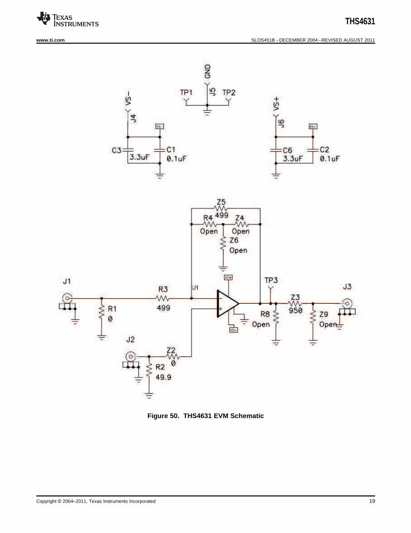
Figure 50. THS4631 EVM Schematic
Copyright © 2004–2011, Texas Instruments Incorporated 19
THS4631
SLOS451B –DECEMBER 2004–REVISED AUGUST 2011 www.ti.com
ADDITIONAL REFERENCE MATERIAL• PowerPAD Made Easy, application brief (SLMA004)• PowerPAD Thermally Enhanced Package, technical brief (SLMA002)• Noise Analysis of FET Transimpedance Amplifiers, application bulletin, Texas Instruments Literature Number
SBOA060.• Tame Photodiodes With Op Amp Bootstrap, application bulletin, Texas Instruments Literature Number
SBBA002.• Designing Photodiode Amplifier Circuits With OPA128, application bulletin, Texas Instruments Literature
Number SBOA061.• Photodiode Monitoring With Op Amps, application bulletin, Texas Instruments Literature Number SBOA035.• Comparison of Noise Performance Between a FET Transimpedance Amplifier and a Switched Integrator,
Application Bulletin, Texas Instruments Literature Number SBOA034.
EVM WARNINGS AND RESTRICTIONS
It is important to operate this EVM within the input and output voltage ranges as specified in the table providedbelow.
Input Range, VS+ to VS– 10 V to 30 V
Input Range, VI 10 V to 30 V NOT TO EXCEED VS+ or VS–Output Range, VO 10 V to 30 V NOT TO EXCEED VS+ or VS–
Exceeding the specified input range may cause unexpected operation and/or irreversible damage to the EVM. Ifthere are questions concerning the input range, please contact a TI field representative prior to connecting theinput power.
Applying loads outside of the specified output range may result in unintended operation and/or possiblepermanent damage to the EVM. Consult the product data sheet or EVM user's guide (if user's guide is available)prior to connecting any load to the EVM output. If there is uncertainty as to the load specification, please contacta TI field representative.
During normal operation, some circuit components may have case temperatures greater than 30°C. The EVM isdesigned to operate properly with certain components above 50°C as long as the input and output ranges aremaintained. These components include but are not limited to linear regulators, switching transistors, passtransistors, and current sense resistors. These types of devices can be identified using the EVM schematiclocated in the material provided. When placing measurement probes near these devices during operation, pleasebe aware that these devices may be very warm to the touch.
Mailing Address: Texas Instruments Post Office Box 655303 Dallas, Texas 75265
20 Copyright © 2004–2011, Texas Instruments Incorporated
THS4631
www.ti.com SLOS451B –DECEMBER 2004–REVISED AUGUST 2011
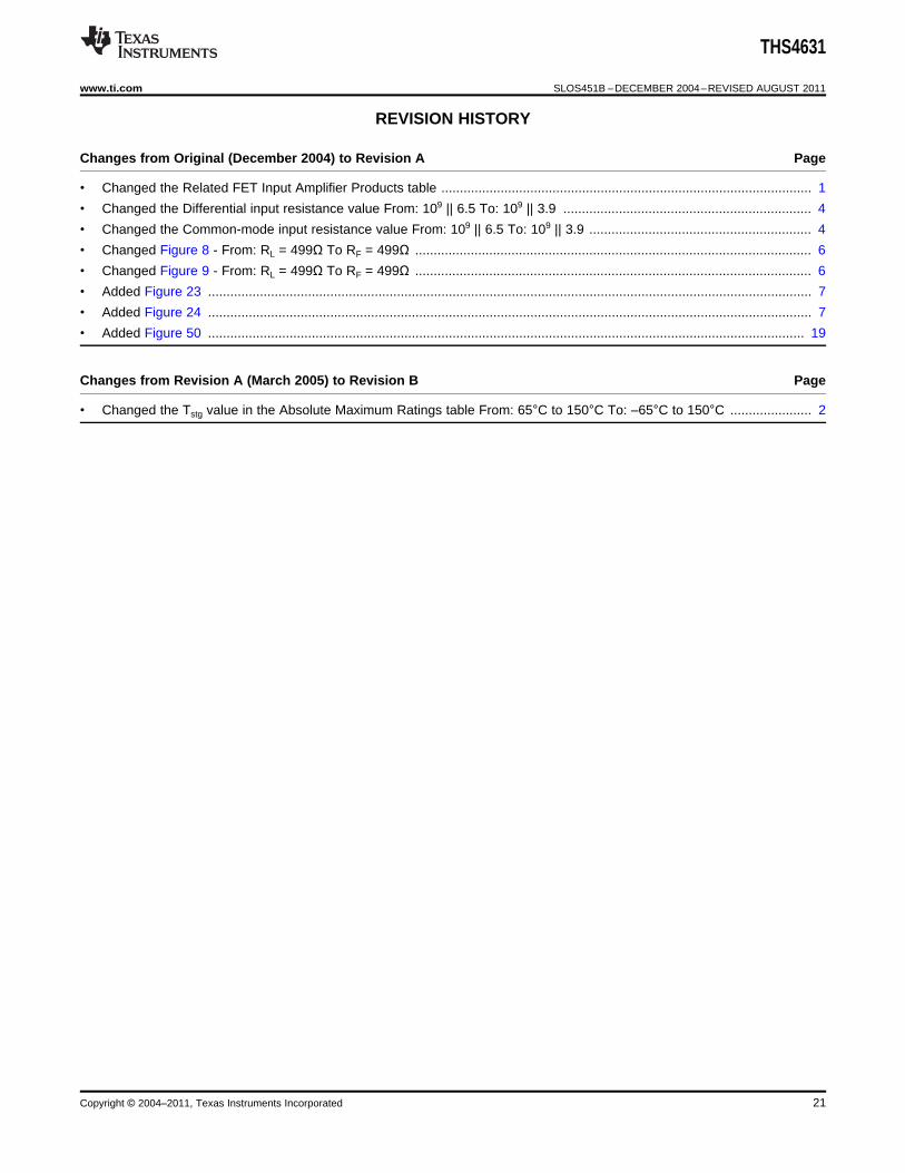
REVISION HISTORY
Changes from Original (December 2004) to Revision A Page
• Changed the Related FET Input Amplifier Products table .................................................................................................... 1
• Changed the Differential input resistance value From: 109 || 6.5 To: 109 || 3.9 ................................................................... 4
• Changed the Common-mode input resistance value From: 109 || 6.5 To: 109 || 3.9 ............................................................ 4
• Changed Figure 8 - From: RL = 499Ω To RF = 499Ω ........................................................................................................... 6
• Changed Figure 9 - From: RL = 499Ω To RF = 499Ω ........................................................................................................... 6
• Added Figure 23 ................................................................................................................................................................... 7
• Added Figure 24 ................................................................................................................................................................... 7
• Added Figure 50 ................................................................................................................................................................. 19
Changes from Revision A (March 2005) to Revision B Page
• Changed the Tstg value in the Absolute Maximum Ratings table From: 65°C to 150°C To: –65°C to 150°C ...................... 2
Copyright © 2004–2011, Texas Instruments Incorporated 21
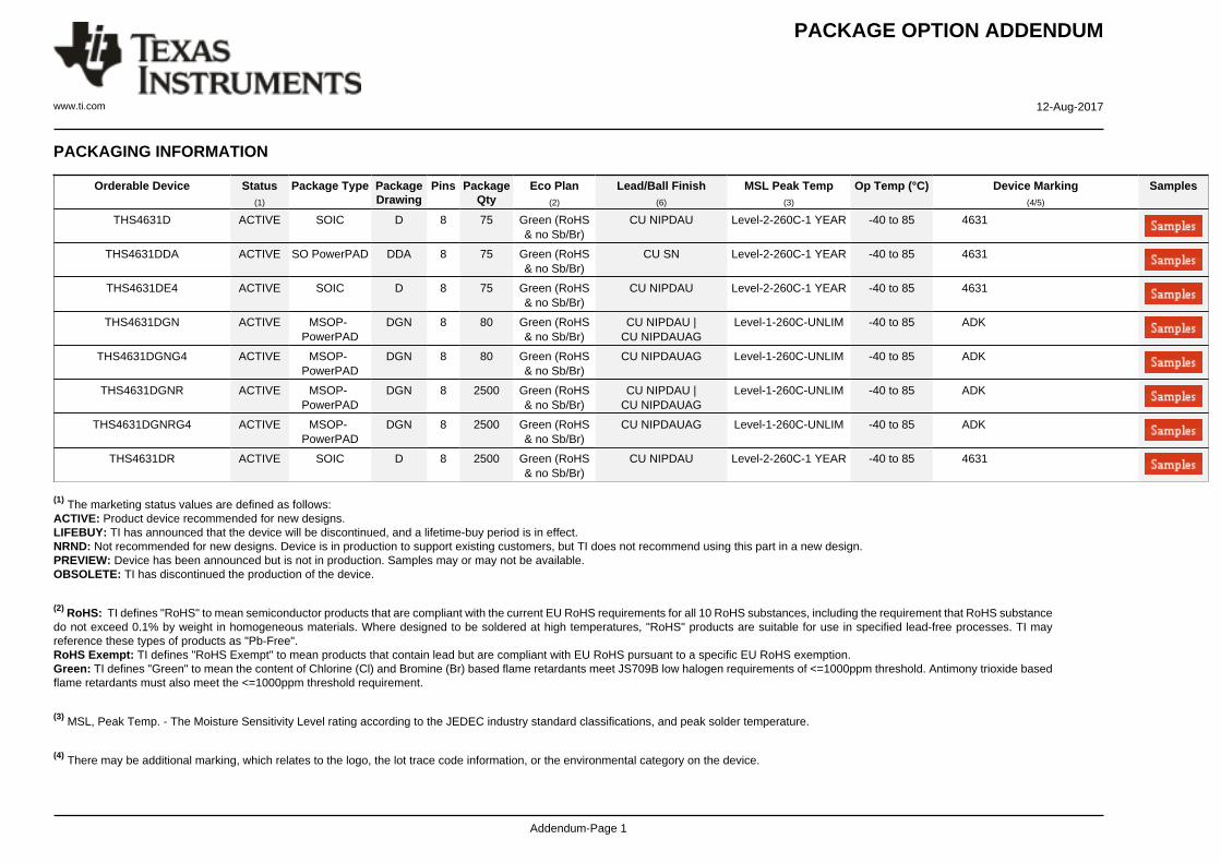
PACKAGE OPTION ADDENDUM
www.ti.com 12-Aug-2017
Addendum-Page 1
PACKAGING INFORMATION
Orderable Device Status(1)
Package Type PackageDrawing
Pins PackageQty
Eco Plan(2)
Lead/Ball Finish(6)
MSL Peak Temp(3)
Op Temp (°C) Device Marking(4/5)
Samples
THS4631D ACTIVE SOIC D 8 75 Green (RoHS& no Sb/Br)
CU NIPDAU Level-2-260C-1 YEAR -40 to 85 4631
THS4631DDA ACTIVE SO PowerPAD DDA 8 75 Green (RoHS& no Sb/Br)
CU SN Level-2-260C-1 YEAR -40 to 85 4631
THS4631DE4 ACTIVE SOIC D 8 75 Green (RoHS& no Sb/Br)
CU NIPDAU Level-2-260C-1 YEAR -40 to 85 4631
THS4631DGN ACTIVE MSOP-PowerPAD
DGN 8 80 Green (RoHS& no Sb/Br)
CU NIPDAU |CU NIPDAUAG
Level-1-260C-UNLIM -40 to 85 ADK
THS4631DGNG4 ACTIVE MSOP-PowerPAD
DGN 8 80 Green (RoHS& no Sb/Br)
CU NIPDAUAG Level-1-260C-UNLIM -40 to 85 ADK
THS4631DGNR ACTIVE MSOP-PowerPAD
DGN 8 2500 Green (RoHS& no Sb/Br)
CU NIPDAU |CU NIPDAUAG
Level-1-260C-UNLIM -40 to 85 ADK
THS4631DGNRG4 ACTIVE MSOP-PowerPAD
DGN 8 2500 Green (RoHS& no Sb/Br)
CU NIPDAUAG Level-1-260C-UNLIM -40 to 85 ADK
THS4631DR ACTIVE SOIC D 8 2500 Green (RoHS& no Sb/Br)
CU NIPDAU Level-2-260C-1 YEAR -40 to 85 4631
(1) The marketing status values are defined as follows:ACTIVE: Product device recommended for new designs.LIFEBUY: TI has announced that the device will be discontinued, and a lifetime-buy period is in effect.NRND: Not recommended for new designs. Device is in production to support existing customers, but TI does not recommend using this part in a new design.PREVIEW: Device has been announced but is not in production. Samples may or may not be available.OBSOLETE: TI has discontinued the production of the device.
(2) RoHS: TI defines "RoHS" to mean semiconductor products that are compliant with the current EU RoHS requirements for all 10 RoHS substances, including the requirement that RoHS substancedo not exceed 0.1% by weight in homogeneous materials. Where designed to be soldered at high temperatures, "RoHS" products are suitable for use in specified lead-free processes. TI mayreference these types of products as "Pb-Free".RoHS Exempt: TI defines "RoHS Exempt" to mean products that contain lead but are compliant with EU RoHS pursuant to a specific EU RoHS exemption.Green: TI defines "Green" to mean the content of Chlorine (Cl) and Bromine (Br) based flame retardants meet JS709B low halogen requirements of <=1000ppm threshold. Antimony trioxide basedflame retardants must also meet the <=1000ppm threshold requirement.
(3) MSL, Peak Temp. - The Moisture Sensitivity Level rating according to the JEDEC industry standard classifications, and peak solder temperature.
(4) There may be additional marking, which relates to the logo, the lot trace code information, or the environmental category on the device.
PACKAGE OPTION ADDENDUM
www.ti.com 12-Aug-2017
Addendum-Page 2
(5) Multiple Device Markings will be inside parentheses. Only one Device Marking contained in parentheses and separated by a "~" will appear on a device. If a line is indented then it is a continuationof the previous line and the two combined represent the entire Device Marking for that device.
(6) Lead/Ball Finish - Orderable Devices may have multiple material finish options. Finish options are separated by a vertical ruled line. Lead/Ball Finish values may wrap to two lines if the finishvalue exceeds the maximum column width.
Important Information and Disclaimer:The information provided on this page represents TI's knowledge and belief as of the date that it is provided. TI bases its knowledge and belief on informationprovided by third parties, and makes no representation or warranty as to the accuracy of such information. Efforts are underway to better integrate information from third parties. TI has taken andcontinues to take reasonable steps to provide representative and accurate information but may not have conducted destructive testing or chemical analysis on incoming materials and chemicals.TI and TI suppliers consider certain information to be proprietary, and thus CAS numbers and other limited information may not be available for release.
In no event shall TI's liability arising out of such information exceed the total purchase price of the TI part(s) at issue in this document sold by TI to Customer on an annual basis.
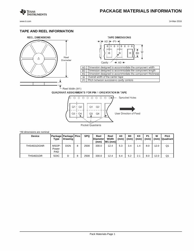
TAPE AND REEL INFORMATION
*All dimensions are nominal
Device PackageType
PackageDrawing
Pins SPQ ReelDiameter
(mm)
ReelWidth
W1 (mm)
A0(mm)
B0(mm)
K0(mm)
P1(mm)
W(mm)
Pin1Quadrant
THS4631DGNR MSOP-Power PAD
DGN 8 2500 330.0 12.4 5.3 3.4 1.4 8.0 12.0 Q1
THS4631DR SOIC D 8 2500 330.0 12.4 6.4 5.2 2.1 8.0 12.0 Q1
PACKAGE MATERIALS INFORMATION
www.ti.com 14-Mar-2016
Pack Materials-Page 1
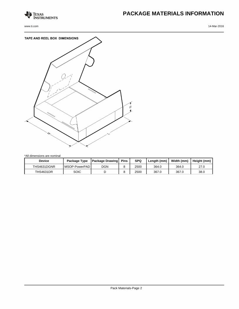
*All dimensions are nominal
Device Package Type Package Drawing Pins SPQ Length (mm) Width (mm) Height (mm)
THS4631DGNR MSOP-PowerPAD DGN 8 2500 364.0 364.0 27.0
THS4631DR SOIC D 8 2500 367.0 367.0 38.0
PACKAGE MATERIALS INFORMATION
www.ti.com 14-Mar-2016
Pack Materials-Page 2
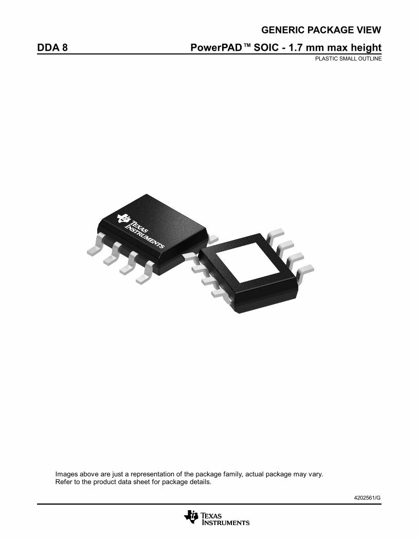
GENERIC PACKAGE VIEW
Images above are just a representation of the package family, actual package may vary.Refer to the product data sheet for package details.
DDA 8 PowerPAD TM SOIC - 1.7 mm max heightPLASTIC SMALL OUTLINE
4202561/G
IMPORTANT NOTICE
Texas Instruments Incorporated (TI) reserves the right to make corrections, enhancements, improvements and other changes to itssemiconductor products and services per JESD46, latest issue, and to discontinue any product or service per JESD48, latest issue. Buyersshould obtain the latest relevant information before placing orders and should verify that such information is current and complete.TI’s published terms of sale for semiconductor products (http://www.ti.com/sc/docs/stdterms.htm) apply to the sale of packaged integratedcircuit products that TI has qualified and released to market. Additional terms may apply to the use or sale of other types of TI products andservices.Reproduction of significant portions of TI information in TI data sheets is permissible only if reproduction is without alteration and isaccompanied by all associated warranties, conditions, limitations, and notices. TI is not responsible or liable for such reproduceddocumentation. Information of third parties may be subject to additional restrictions. Resale of TI products or services with statementsdifferent from or beyond the parameters stated by TI for that product or service voids all express and any implied warranties for theassociated TI product or service and is an unfair and deceptive business practice. TI is not responsible or liable for any such statements.Buyers and others who are developing systems that incorporate TI products (collectively, “Designers”) understand and agree that Designersremain responsible for using their independent analysis, evaluation and judgment in designing their applications and that Designers havefull and exclusive responsibility to assure the safety of Designers' applications and compliance of their applications (and of all TI productsused in or for Designers’ applications) with all applicable regulations, laws and other applicable requirements. Designer represents that, withrespect to their applications, Designer has all the necessary expertise to create and implement safeguards that (1) anticipate dangerousconsequences of failures, (2) monitor failures and their consequences, and (3) lessen the likelihood of failures that might cause harm andtake appropriate actions. Designer agrees that prior to using or distributing any applications that include TI products, Designer willthoroughly test such applications and the functionality of such TI products as used in such applications.TI’s provision of technical, application or other design advice, quality characterization, reliability data or other services or information,including, but not limited to, reference designs and materials relating to evaluation modules, (collectively, “TI Resources”) are intended toassist designers who are developing applications that incorporate TI products; by downloading, accessing or using TI Resources in anyway, Designer (individually or, if Designer is acting on behalf of a company, Designer’s company) agrees to use any particular TI Resourcesolely for this purpose and subject to the terms of this Notice.TI’s provision of TI Resources does not expand or otherwise alter TI’s applicable published warranties or warranty disclaimers for TIproducts, and no additional obligations or liabilities arise from TI providing such TI Resources. TI reserves the right to make corrections,enhancements, improvements and other changes to its TI Resources. TI has not conducted any testing other than that specificallydescribed in the published documentation for a particular TI Resource.Designer is authorized to use, copy and modify any individual TI Resource only in connection with the development of applications thatinclude the TI product(s) identified in such TI Resource. NO OTHER LICENSE, EXPRESS OR IMPLIED, BY ESTOPPEL OR OTHERWISETO ANY OTHER TI INTELLECTUAL PROPERTY RIGHT, AND NO LICENSE TO ANY TECHNOLOGY OR INTELLECTUAL PROPERTYRIGHT OF TI OR ANY THIRD PARTY IS GRANTED HEREIN, including but not limited to any patent right, copyright, mask work right, orother intellectual property right relating to any combination, machine, or process in which TI products or services are used. Informationregarding or referencing third-party products or services does not constitute a license to use such products or services, or a warranty orendorsement thereof. Use of TI Resources may require a license from a third party under the patents or other intellectual property of thethird party, or a license from TI under the patents or other intellectual property of TI.TI RESOURCES ARE PROVIDED “AS IS” AND WITH ALL FAULTS. TI DISCLAIMS ALL OTHER WARRANTIES ORREPRESENTATIONS, EXPRESS OR IMPLIED, REGARDING RESOURCES OR USE THEREOF, INCLUDING BUT NOT LIMITED TOACCURACY OR COMPLETENESS, TITLE, ANY EPIDEMIC FAILURE WARRANTY AND ANY IMPLIED WARRANTIES OFMERCHANTABILITY, FITNESS FOR A PARTICULAR PURPOSE, AND NON-INFRINGEMENT OF ANY THIRD PARTY INTELLECTUALPROPERTY RIGHTS. TI SHALL NOT BE LIABLE FOR AND SHALL NOT DEFEND OR INDEMNIFY DESIGNER AGAINST ANY CLAIM,INCLUDING BUT NOT LIMITED TO ANY INFRINGEMENT CLAIM THAT RELATES TO OR IS BASED ON ANY COMBINATION OFPRODUCTS EVEN IF DESCRIBED IN TI RESOURCES OR OTHERWISE. IN NO EVENT SHALL TI BE LIABLE FOR ANY ACTUAL,DIRECT, SPECIAL, COLLATERAL, INDIRECT, PUNITIVE, INCIDENTAL, CONSEQUENTIAL OR EXEMPLARY DAMAGES INCONNECTION WITH OR ARISING OUT OF TI RESOURCES OR USE THEREOF, AND REGARDLESS OF WHETHER TI HAS BEENADVISED OF THE POSSIBILITY OF SUCH DAMAGES.Unless TI has explicitly designated an individual product as meeting the requirements of a particular industry standard (e.g., ISO/TS 16949and ISO 26262), TI is not responsible for any failure to meet such industry standard requirements.Where TI specifically promotes products as facilitating functional safety or as compliant with industry functional safety standards, suchproducts are intended to help enable customers to design and create their own applications that meet applicable functional safety standardsand requirements. Using products in an application does not by itself establish any safety features in the application. Designers mustensure compliance with safety-related requirements and standards applicable to their applications. Designer may not use any TI products inlife-critical medical equipment unless authorized officers of the parties have executed a special contract specifically governing such use.Life-critical medical equipment is medical equipment where failure of such equipment would cause serious bodily injury or death (e.g., lifesupport, pacemakers, defibrillators, heart pumps, neurostimulators, and implantables). Such equipment includes, without limitation, allmedical devices identified by the U.S. Food and Drug Administration as Class III devices and equivalent classifications outside the U.S.TI may expressly designate certain products as completing a particular qualification (e.g., Q100, Military Grade, or Enhanced Product).Designers agree that it has the necessary expertise to select the product with the appropriate qualification designation for their applicationsand that proper product selection is at Designers’ own risk. Designers are solely responsible for compliance with all legal and regulatoryrequirements in connection with such selection.Designer will fully indemnify TI and its representatives against any damages, costs, losses, and/or liabilities arising out of Designer’s non-compliance with the terms and provisions of this Notice.
Mailing Address: Texas Instruments, Post Office Box 655303, Dallas, Texas 75265Copyright © 2018, Texas Instruments Incorporated