Embed Size (px)
Citation preview
SPIE 2000, Vol. 3999-40
1
Development of Analysis System for F2-Excimer Laser Photochemical Processes
Atsushi Sekiguchi, Mikio Kadoi, Yasuhiro Miyake, Toshiharu Matsuzawa, and Chris A. Mack*
Litho Tech Japan Corporation Kawaguchi, Saitama, 332-0034, Japan
*FINLE Technologies, A Division of KLA-Tencor Austin, TX
[email protected], [email protected]
Abstract
A system for photochemical analysis of F2-excimer laser lithography processes has been developed. The system, VUVES-4500, consists of 3 units: (1) an exposure and bake unit that uses the F2-excimer laser to carry out a flood exposure and then post-exposure bake (PEB) of a resist coated wafer, (2) a unit for the measurement of development rate of photoresists, and (3) a simulation unit that utilizes PROLITH to calculate the resist profiles and process latitude using the measured development rate data. With this system, preliminary evaluation of the performance of F2 excimer laser lithography can be performed without a lithography tool that is capable of imaging and alignment. Profiles for 100 nm lines are simulated for the PAR-101 resist (manufactured by Sumitomo Chemical) and the SAL-601 resist (manufactured by Shipley), a chemically amplified resist that has sensitivity at the F2 excimer laser wavelength. The simulation successfully predicts the resist behavior. Thus, it is confirmed that the system enables efficient evaluation of the performance of F2 excimer laser lithography processes.
Keywords: chemically amplified resist, lithography simulation, F2 excimer laser, resist development rates, exposure tool, homogenizer optical system
1. Introduction In developing new resists, ordinarily a projection printing tool (a "stepper") capable of direct evaluation of the resolving properties and process tolerance is thought to be necessary [1]. However, work to develop a stepper for use with F2 excimer lasers has just begun, and it is thought that considerable time will be
2
needed before practical F2 excimer laser steppers become available. In addition, resists are needed in order to assess the lens aberrations and resolution of the stepper during development, so that stepper development and resist development are in a chicken-and-egg relationship [2]. Thus, in order to accelerate stepper development, progress must be made in developing resist materials. Given this situation, there is a need for a system for evaluating new resists without requiring a stepper. We have used a combination of experiment and lithography simulation to develop the VUVES-4500, the Vacuum Ultraviolet Excimer Laser Process Evaluation System for photochemical analysis of new F2 excimer laser processes without requiring a stepper. Using this new system, we have studied the F2 excimer laser exposure of two existing resists: PAR-101 (a positive resist designed for 193 nm exposure from Sumitomo Chemical) [3], and SAL-601 (a negative electron beam resist from Shipley) [4]. Herein we report our results.
2. System Configuration VUVES-4500 consists of the following three base units: (1) An exposure unit which uses F2 excimer laser light for resist exposure, and also performs post-exposure
baking (PEB) and cooling. (2) A unit for measurement and analysis of resist development rates for different exposure doses. (3) A simulator unit which employs the accumulated development data in numerical calculation of resist
profiles and process margins.
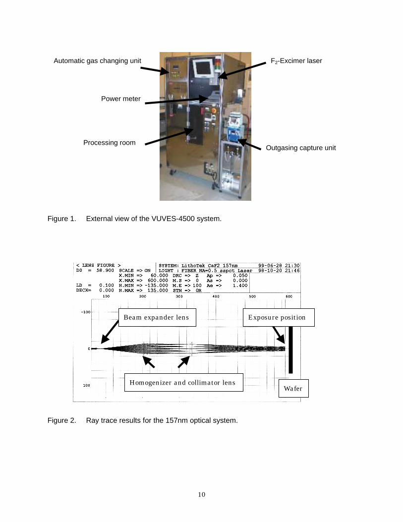
2.1 Exposure and baking unit The F2 excimer laser exposure, PEB and cooling unit consists of an F2 excimer laser light source, optical system, exposure stage, PEB baking plate, cooling plate, and wafer transfer robot. Figure 1 is an external view of the exposure and baking unit. The 157 nm laser light leaving the laser light source passes through an electronic shutter and is broadened by a beam expander lens. It then passes through a two-stage optical system with an array of 25 homogenizers (5x5) to be formed into a parallel ray, before passing through a collimator and impinging on the resist. The homogenizer optical system must efficiently pass laser light at 157 nm, and so employs CaF2. Throughout the entire optical path all air is replaced by N2. The exposure area
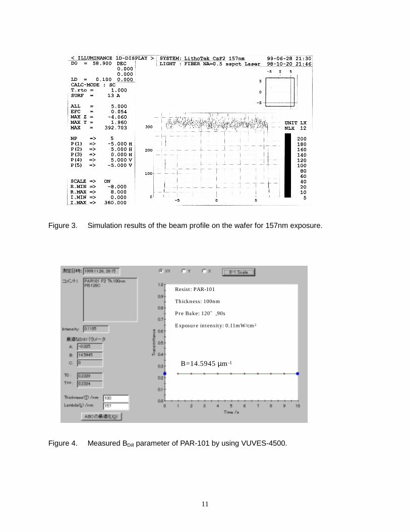
is an open frame 8 mm on a side; in-plane uniformity within the exposed area is ±5%. Figure 2 shows the results of optical path simulations for the homogenizer optical system. Figure 3 shows simulated results for the beam profile on the wafer by light which has been split by the homogenizer lenses after passing through the homogenizer optical system. The exposure dose is controlled by placing a half-mirror in the optical path and monitoring the exposure energy in situ. The exposure dose can be set in the range 0.01 to 500 mJ/cm2, varied
3
in 0.01 mJ/cm2 steps. When exposure is completed, the robot transports the sample to the load/lock PEB baking plate. The PEB baking plate is positioned within the exposure system, and the air along the wafer transport line can be replaced using a chemical filter. This holds to an absolute minimum amine contaminants in the atmosphere between the completion of exposure and PEB, thus reducing the Post Exposure Delay (PED) effect. And by adopting a load/lock-type PEB baking plate, any diffusion of outgas products generated during PEB into the exposure chamber can be prevented. When PEB is completed, the transfer robot carries the sample to the cooling plate for cooling. Immediately after PEB the wafer is quickly cooled, so that any residual deprotection reaction is suppressed. The time from PEB until cooling can be freely adjusted, so that the effect of this residual deprotection reaction can be studied. Further, a power sensor for measurement of transmittance was embedded in the exposure stage. By this means the transmittance of the resist material can be measured. The procedure for transmittance measurement is as follows. First, an MgF2 substrate with no resist applied is placed on an exposure stage and irradiated with 157 nm laser light to perform system calibration. The transmittance at this time is taken to be 100%. Next, a sample with resist applied to an MgF2 substrate is placed on the stage, and the transmittance of the resist material measured. By substituting the transmittance thus obtained in equation (1), the Dill B parameter [5] can be determined. Figure 4 shows an example of PAR-101 transmittance measurements and determination of the Dill’s B parameter.
( )∞
−= T
dB ln1 (1)
Here, B is the Dill’s B parameter (µm-1), d is resist thickness (µm), and T∞ is the final transmittance of the exposed film.
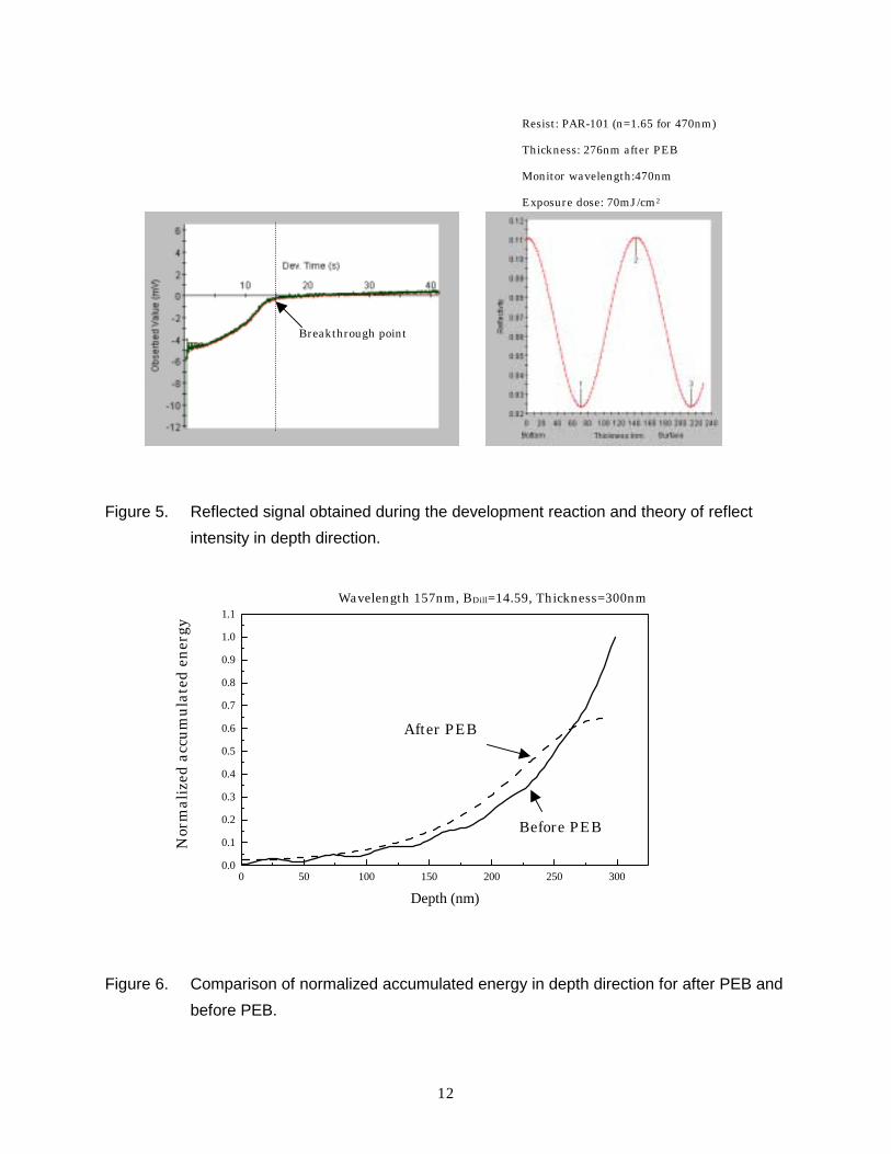
2.2 Unit for measurement and analysis of resist development characteristics This unit adopts a resist development analyzer [6] developed by us. The development rate of the resist is measured by shining monochromatic light on a thin film of the resist during development. When monochromatic light is incident on the resist film during development, the light reflected from the film surface interferes with the light reflected from the substrate surface. As the film thickness changes with development, the reflection intensity is observed to vary sinusoidally with development time. By using the Dill theory of interference in thin films, the interference waveform obtained can be converted into a development rate [7]. Figure 5 shows measurement results for light reflected from PAR-101 irradiated with F2 excimer laser light.
4
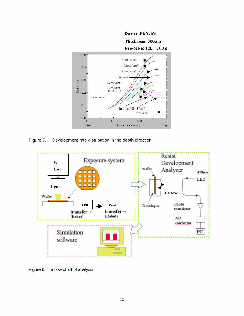
The film thickness is 300 nm. Ordinarily at this film thickness there will be at least three fringe peaks, as in the theoretical waveform shown in the figure. But as Figure 5 indicates, no fringe peaks appear, and there is only a monotonic increase in signal over time. The cause of this is thought to be that, instead of the development proceeding layer by layer, irregular development in microscopic areas occurs, so that the monitoring light is scattered at the development interface [8]. Thus, the usual Dill thin film interference theory cannot be applied to obtain the development rate in a resist film using data on reflected light. Hence an approach was proposed for predicting the depth-direction development rate profile by using a method in which the accumulated energy distribution in the resist film is calculated [9]. This method is described below. From Figure 5, the so-called breakthrough time, at which the resist film is completely gone, can easily be determined (the breakthrough point in Figure 5). By this means, the average development rate over the time from the start of development until the resist is completely gone can be determined. On the other hand, using the measured value of the Dill’s B parameter discussed in the previous section, the theoretical distribution of accumulated energy in the resist film due to exposure can be determined (with calculations taking PEB into account), as seen in Figure 6. The accumulated energy value is thought to be proportional to the acid concentration (H+) from PAG. If the depth-direction accumulated energy distribution is integrated with respect to the resist depth, the average accumulated energy can be found. And if both these calculations are performed for different exposure doses, the relation between the average accumulated energy and the average development rate can be obtained. By applying this to Mack's original development rate equation [10], the relation between accumulated energy and development rate can be found. Further, this equation can be used to convert the depth-direction accumulated energy distribution in Figure 6 into a development rate distribution, enabling calculation of the development rate R(E,Z) at different depths in the resist film for different exposure doses. Here, R is the development rate, E is the exposure dose, and Z is the depth in the resist. This method employs the Dill’s B parameter, and so even in F2 exposure where development irregularity means thin film interference cannot be obtained, it is still possible to predict the development rate taking into account the effect of absorption in the resist film. Figure 7 shows the development rate distribution in the depth direction for
PAR-101 at 300nm resist thickness (the prebake condition was 120°C, 60s and the PEB condition was 120°C, 60s) [11].
2.3 Lithography simulation unit The lithography simulation unit adopts FINLE's PROLITH/2 (Positive Resist Optical LITHography model) [12]. This software is capable of simulating the basic steps of lithography, including imaging, resist exposure (generation of photoacids), PEB-induced deprotection reactions, and development, to calculate the final resist profile. Optical intensities can be calculated based on scalar diffraction theory using the extended source method to determine the optical intensity resulting from a projection optical system with partial
5
coherence and aberrations, taking defocusing effects into account. Corrections for high NA are also performed, to more faithfully reproduce the effects of imaging in the resist film. Initially, the photoacid distribution induced in the resist film by exposure is calculated. That is, Dill's A, B and C parameters [5] are used to convert the optical intensity distribution in the film into a photoacid concentration distribution. Then, PEB-induced secondary photoacid diffusion is calculated, and dissociation of protection groups due to catalytic action of the acid is computed. The acid loss function of the photoacid can also be included in calculations. Development calculations are performed by converting the concentration distribution of the protection groups thus obtained into a development rate distribution using the development parameters. Through this series of calculations, the final resist profile is obtained. The calculation model described above is called a physical calculation model. However, in many chemically amplified resists bleaching does not occur (parameter A=0), making it difficult to determine the Dill’s C parameter [9]. In F2 excimer laser exposure, there are no changes in transmittance due to exposure, as shown in Figure 4, and the C parameter cannot be calculated. Also, the reaction and diffusion parameters during PEB are often not known. Hence in this system, instead of using the C parameter and the development parameters, the exposure energy and development rate data table R(E,Z) is used directly to calculate immediately the development rate distribution from the optical intensity distribution incident on the film, thus performing measurement-based simulations to calculate development data [11]. Thus, it is possible to perform simulations without calculating the Dill’s C parameter, development parameters, deprotection reaction parameters, or other parameters for physical-model simulation. Further, the R(E,Z) data table used here takes into account the effect of absorption in the resist film using the Dill’s B parameter, and this method introduces the principle of calculations used in physical-model simulations, in a new type of model which merges physical-model simulation and measured-value simulation. By using this method, it is possible to simulate new lithography processes for which a model has not yet been established, such as F2 excimer laser exposure. And this method includes the PED effect [13] and other factors, and so makes possible simulations that more nearly approximate actual conditions. Using the above three process analysis units, it is possible to perform sample exposure, development rate analysis, and simulations to quickly assess F2 excimer laser processes. Figure 8 illustrates the flow of processing from exposure to simulation.
3. Experimental
3.1 Development analysis This system was used with PAR-101 positive chemically amplified resist compatible with ArF excimer
6
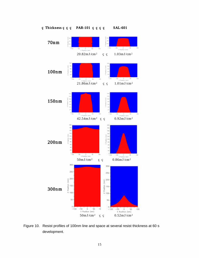
lasers, and SAL-601 negative chemically amplified resist for electron beam lithography, in F2 excimer laser exposure, development analysis, and simulations. The optimum film thickness was also studied. Experimental conditions appear in Table 1. Development was performed in both cases by the dip method using NMD-3 (TMAH 2.38%) at 23°C. Figure 9(a) shows the development discrimination curve for PAR-101 at different film thicknesses. Here exposure doses ranged from 0 to 50 mJ/cm2, and film thicknesses were 70 nm, 100 nm, 150 nm, 200 nm, and 300 nm. Adequate discrimination is obtained at film thicknesses of 70 and 100 nm, but at 150 nm and above the discrimination curve divides into two regions, and sufficient discrimination is not obtained. Table 2 shows
measured values of Eth, γ, and tanθ for different film thicknesses. Here the higher the numerical value, the higher is the resist contrast. There is thought to be a correlation between tanθ and the limiting resolution [14]. It was found that the thinner the film, the higher is tanθ, that is, the higher is the resist contrast. At a thickness of 300 nm, there is no resist contrast, and even after an exposure dose of 50 mJ/cm2 and development for 60 seconds, the resist was not dissolved down to the substrate. Figure 9(b) shows the discrimination curve for development of SAL-601 after F2 excimer laser exposure. The exposure dose was the same as for PAR-101, from 0 to 50 mJ/cm2. Film thicknesses were 70 nm, 100 nm, 150 nm, 200 nm, and 300 nm. As indicated in Figure 9(b), discrimination for SAL-601 is similar for all film thicknesses. Table 3 shows measured values of the dose to clear (Eth), the conventionally measured
contrast (γ), and the theoretical contrast (tanθ) for different film thicknesses. In the case of SAL-601, both γ and tanθ remained nearly constant and were independent of the resist film thickness.
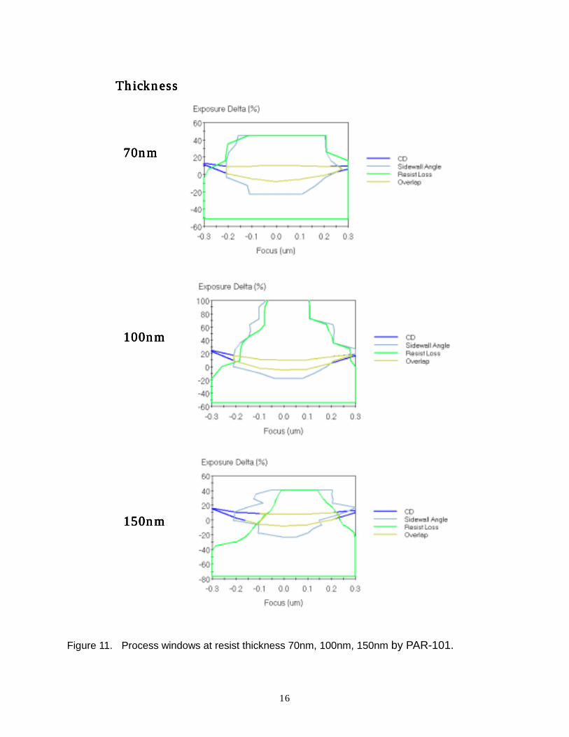
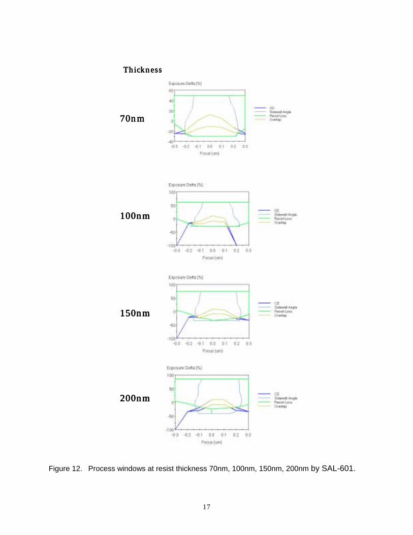
3.2 Profile simulations The simulation conditions are described below. The exposure wavelength was 157 nm; the numerical aperture was 0.7, and the irradiation system coherence factor was taken to be 0.6. The calculated development rate data R(E,Z) resulting from F2 excimer laser exposure of both resists were input to the simulator, and profile calculations performed for a 100 nm line/space pattern. Simulation results appear in Figure 10. It is seen that a nearly vertical profile is obtained for PAR-101 resist film of thickness 70 nm. As the film thickness is increased, the profile deteriorates, and at 200 nm and greater pattern resolution is no longer obtained. At SAL-601 resist film thicknesses of 70 nm and 100 nm the pattern top is somewhat rounded, but resolution is obtained. At thicknesses of 150 nm and 200 nm, though resolution is obtained there is considerable tapering of the pattern side walls, and good quality patterns are not obtained. At a film thickness of 300 nm, pattern resolution was not obtained. Figure 11 shows the PAR-101 process window. At 70 nm, the widest process window is obtained; as the film thickness is increased, the process window narrows, and at 200 nm and above no process window was obtained. On the other hand, Figure 12 shows the process window for SAL-601. Here
7
the widest process window was obtained for a 70 nm SAL-601 film. Process windows with about the same margin were obtained at film thicknesses of 100 nm to 200 nm; at 300 nm, no process window was obtained. Compared with a film thickness of 70 nm, a wider process window was obtained for PAR-101 than for SAL-601.
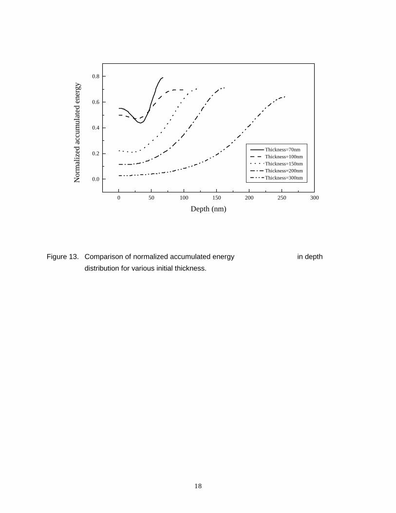
3.3 Discussion Resolution characteristics at 157nm exposure in PAR-101 positive chemically amplified resist and in SAL-601 negative chemically amplified resist were studied for different film thicknesses. In both types of resist, the best resist profiles and process windows were obtained at a film thickness of 70 nm. On the other hand, pattern resolution was not obtained in either resist at a film thickness of 300 nm. The reason for this is thought to be the following. Figure 13 shows the normalized distribution of energy accumulated in the film, assuming both types of resist. At a film thickness of 70 nm, the normalized accumulated energy in the resist film near the substrate is approximation 0.3 for PAR-101 and 0.35 for SAL-601; in contrast, when the film thickness is 300 nm the normalized accumulated energies near the substrate are 0.01 and 0.02, so that almost no radiation reaches the substrate when the film is 300 nm thickness. Thus, when a resist with strong absorption,
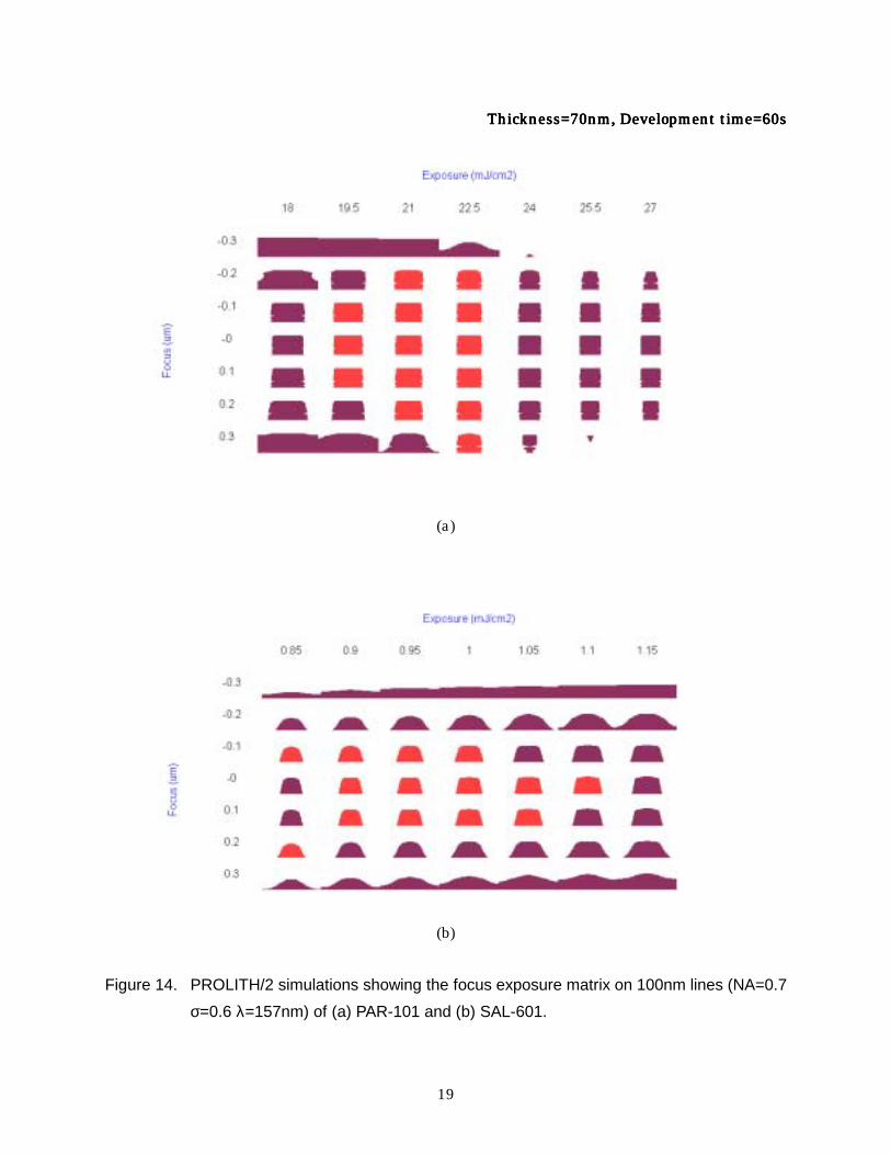
with B between 12 and 15 µm-1 or so, is used in F2 exposure, the resist film must be made thin, and it is anticipated that at a film thickness of 70 nm or so, patterning is possible. Figure 14 shows the defocusing characteristics at 100 nm L/S for films of both resist types of thickness 70 nm; Figure 15 shows the results of
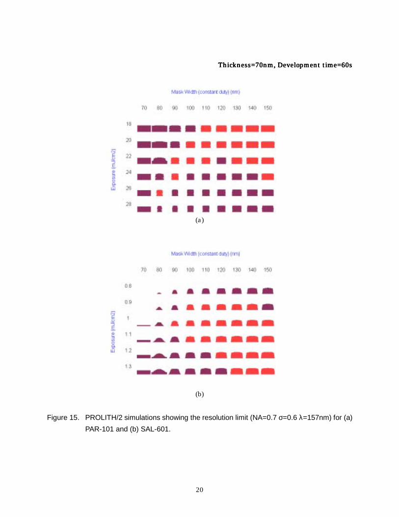
simulations near the limiting resolution. From Figure 14, a depth of focus of 0.5 µm is obtained for PAR-101, and a depth of focus of 0.4 µm for SAL-601. Moreover, use of this system enabled the prediction, based on Figure 15, that resolution is possible down to 80 nm for PAR-101 and down to 90 nm for SAL-601.
4. Conclusions A system for photochemical analysis using F2 excimer laser light, VUVES-4500, was developed. Using this system, 100 nm pattern profiles resulting from exposure of a positive resist for ArF excimer lasers and a negative resist for electron beam exposure to F2 excimer laser light were studied. By using this system, it was confirmed that resolution of 100 nm patterns is possible even when using a strongly absorptive resist by making the resist film thin. Moreover, this result suggests the possibility of studying F2 excimer laser resist materials for which a simulation model has not yet been established, to enable not only optimization of baking conditions, film thickness, development conditions and other process parameters, but prompt examination of resolution limits when using ultra-high resolution techniques as well.
8
Acknowledgements The authors are grateful to Mr. Itoh of the Optical Systems Research Laboratory in the system design, and to Senior Researcher Dr. Uetani of Sumitomo Chemical and Mr. Kawabata of Shipley Far East for providing resist samples.
References [1] V. Pol, J. H. Bennevitz, G. C. Escher, M. Feldam, V. A. Firton, T. E. Jewell, B. E. Wilcomb, and J. T.
Clemens: Proc. SPIE 633 (1986) 186.
[2] A. Sekiguchi, M. Kadoi, Y. Minami and T. Matsuzawa: Semiconductor World 6 (1997) 25.
[3] Y. Uetani and K. Fujishima: Soci. Polymer Science Jan. 8 (1999) 9.
[4] F. Murai, J. Yamamoto, H. Yamaguchi and S. Okazaki: J. Vac. Sci. Technol. B12 (1994) 3874.
[5] F. H. Dill, W. P. Hornberger, P. S. Hauge and J. M. Shaw: IEEE D-22 (1975) 445.
[6] A. Sekiguchi, C. A.Mack, Y. Minami and T. Mastuzawa: Proc. SPIE 2725 (1996) 49.
[7] F. H. Dill, A. R. Neureuther, J. A. Tuttle and E. J. Walker: IEEE D-22 (1975) 456.
[8] T. Ushirogouchi, T. Naito, K. Asakawa, N. Shida, M. Nakase and T. Tada: ACS Symp. Series 16 (1995) 240.
[9] A. Sekiguchi, M.Kadoi, T. Matsuzawa and Y. Minami: Electro. Commun. Jan. pt 2 82 (1999) 30.
[10] C. A. Mack, Inside PROLITH: A Comprehensive Guide to Optical Lithography Simulation, FINLE Technologies (Austin: 1997).
[11] Y. Minami and Sekiguchi: Electro. Communi. Jan. pt 2 J76 (1993) 562.
[12] C. A. Mack, M. J. Maslow, R. Carpio and A. Sekiguchi: Olin Microelec. Materials Interface ’97 Proc. (1997) 203.
[13] T. Ohfiji, A. G. Timko, O. Nalamasu and D. R. Stone: Proc. SPIE 1925 (1993) 213.
[14] A. Sekiguchi, Y. Minami and Y. Sensu: Electrochem. Soci. Jan. 42 (1992) 149.
9
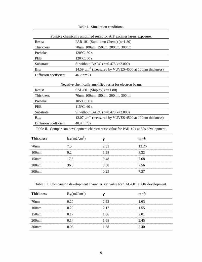
Table I. Simulation conditions.
Positive chemically amplified resist for ArF excimer lasers exposure. Resist PAR-101 (Sumitomo Chem.) (n=1.80) Thickness 70nm, 100nm, 150nm, 200nm, 300nm Prebake 120°C, 60 s PEB 120°C, 60 s Substrate Si without BARC (n=0.478 k=2.000) BDill 14.59 µm-1 (measured by VUVES-4500 at 100nm thickness) Diffusion coefficient 46.7 nm2/s
Negative chemically amplified resist for electron beam. Resist SAL-601 (Shipley) (n=1.80) Thickness 70nm, 100nm, 150nm, 200nm, 300nm Prebake 105°C, 60 s PEB 115°C, 60 s Substrate Si without BARC (n=0.478 k=2.000) BDill 12.07 µm-1 (measured by VUVES-4500 at 100nm thickness) Diffusion coefficient 48.4 nm2/s Table II. Comparison development characteristic value for PAR-101 at 60s development.
Thickness Eth(mJ/cm2) γγγγ tanθθθθ
70nm 7.5 2.31 12.26
100nm 9.2 1.28 8.32
150nm 17.3 0.48 7.68
200nm 36.5 0.38 7.56
300nm 0.25 7.37
Table III. Comparison development characteristic value for SAL-601 at 60s development.
Thickness Eth(mJ/cm2) γγγγ tanθθθθ
70nm 0.20 2.22 1.63
100nm 0.20 2.17 1.55
150nm 0.17 1.86 2.01
200nm 0.14 1.68 2.45
300nm 0.06 1.38 2.40
10
Figure 1. External view of the VUVES-4500 system.
Figure 2. Ray trace results for the 157nm optical system.
F2-Excimer laser Automatic gas changing unit
Power meter
Processing room Outgasing capture unit
Beam expander lens
Homogenizer and collimator lens
Exposure position
Wafer
11
Figure 3. Simulation results of the beam profile on the wafer for 157nm exposure.
Figure 4. Measured BDill parameter of PAR-101 by using VUVES-4500.
Resist: PAR-101
Thickness: 100nm
Pre Bake: 120℃,90s
Exposure intensity: 0.11mW/cm2
B=14.5945 µm-1
12
Figure 5. Reflected signal obtained during the development reaction and theory of reflect
intensity in depth direction. Figure 6. Comparison of normalized accumulated energy in depth direction for after PEB and
before PEB.
Resist: PAR-101 (n=1.65 for 470nm)
Thickness: 276nm after PEB
Monitor wavelength:470nm
Exposure dose: 70mJ/cm2
Breakthrough point
0 50 100 150 200 250 3000.0
0.1
0.2
0.3
0.4
0.5
0.6
0.7
0.8
0.9
1.0
1.1
Acc
umla
ted
ener
gy
Depth (nm)
Before PEB
After PEB
Wavelength 157nm, BDill=14.59, Thickness=300nm
Nor
mal
ized
N
orm
aliz
ed a
ccum
ulat
ed e
nerg
y
13
Figure 7. Development rate distribution in the depth direction.
Figure 8. The flow chart of analysis.
50mJ/cm2 403mJ/cm2 20mJ/cm2
15mJ/cm2 12mJ/cm2 10mJ/cm2 8mJ/cm2
7mJ/cm2
6mJ/cm2 5mJ/cm2 4mJ/cm2
Resist: PARResist: PARResist: PARResist: PAR----101101101101 Thickness: 300Thickness: 300Thickness: 300Thickness: 300nmnmnmnm PrePrePrePre----bake: bake: bake: bake: 120120120120℃℃℃℃, 60 s, 60 s, 60 s, 60 s
℃℃
FFFF2222
LaserLaserLaserLaser
LensLensLensLens
PEBPEBPEBPEB CoolCoolCoolCool
DetectorDetectorDetectorDetector
14
Figure 9. Exposure dose-Development rate curves for (a) PAR-101 and (b) SAL-601.
Resist: PAR-101 Pre-Bake: 120℃, 60 s PEB: 120℃, 60s Without BARC
0.01 0.1 1 10 1001E-4
1E-3
0.01
0.1
1
10
Thickness=70nm Thickness=100nm Thickness=150nm Thickness=200nm Thickness=300nm
Dev
elop
men
t rat
e (n
m/s
)
Exposure dose (mJ/cm2)
Resist: SAL-601 Pre-bake: 105℃, 60 s PEB: 115℃, 60s Without BARC
(a)
(b)
0.1 1 10 1001E-3
0.01
0.1
1
10
100
Thickness=70nm Thickness=100nm Thickness=150nm Thickness=200nm Thickness=300nm
Dev
elop
men
t rat
e (n
m/s
)
Exposure dose (mJ/cm2)
15
Figure 10. Resist profiles of 100nm line and space at several resist thickness at 60 s
development.
70nm70nm70nm70nm 100nm100nm100nm100nm 150nm150nm150nm150nm 200nm200nm200nm200nm 300nm300nm300nm300nm
Thickness Thickness Thickness Thickness PAR PAR PAR PAR----101 101 101 101 SAL SAL SAL SAL----601601601601
20.82mJ/cm2 1.03mJ/cm2
21.86mJ/cm2 1.01mJ/cm2
42.54mJ/cm2 0.92mJ/cm2
50mJ/cm2 0.86mJ/cm2
50mJ/cm2 0.52mJ/cm2
16
Figure 11. Process windows at resist thickness 70nm, 100nm, 150nm by PAR-101.
ThicknessThicknessThicknessThickness 70nm 70nm 70nm 70nm 100nm 100nm 100nm 100nm 150nm 150nm 150nm 150nm
17
Figure 12. Process windows at resist thickness 70nm, 100nm, 150nm, 200nm by SAL-601.
TTTThicknesshicknesshicknesshickness 70nm 70nm 70nm 70nm 100nm 100nm 100nm 100nm 150nm 150nm 150nm 150nm 200nm 200nm 200nm 200nm
18
Figure 13. Comparison of normalized accumulated energy in depth
distribution for various initial thickness.
0 50 100 150 200 250 300
0.0
0.2
0.4
0.6
0.8
Thickness=70nm Thickness=100nm Thickness=150nm Thickness=200nm Thickness=300nmN
orm
aliz
ed a
ccum
ulat
ed e
nerg
y
Depth (nm)
19
Thickness=70nm, DevThickness=70nm, DevThickness=70nm, DevThickness=70nm, Development time=60selopment time=60selopment time=60selopment time=60s
(a)
(b)
Figure 14. PROLITH/2 simulations showing the focus exposure matrix on 100nm lines (NA=0.7
σ=0.6 λ=157nm) of (a) PAR-101 and (b) SAL-601.
20
Thickness=70nm, Development time=60sThickness=70nm, Development time=60sThickness=70nm, Development time=60sThickness=70nm, Development time=60s
(a)
(b)
Figure 15. PROLITH/2 simulations showing the resolution limit (NA=0.7 σ=0.6 λ=157nm) for (a)
PAR-101 and (b) SAL-601.


![Synthesis and Photophysical Properties of … and...because of useful photophysical and photochemical properties of these compounds [1–7]. BF 2bdks ex-hibit large extinction coefficients,](https://img.pdfslide.tips/doc/110x75/5ed232bfb2660731f56544f4/synthesis-and-photophysical-properties-of-and-because-of-useful-photophysical.jpg)