Embed Size (px)
Citation preview
Developmentofnovelelectricalcharacteriza‐
tionmethodsandmeasurementsofG4‐DNA
andDNADerivatives
Thesissubmittedforthedegreeof
“DoctorofPhilosophy”
by
GideonLivshits
SubmittedtotheSenateof
TheHebrewUniversityofJerusalem
October2014
Developmentofnovelelectricalcharacteriza‐
tionmethodsandmeasurementsofG4‐DNA
andDNADerivatives
Thesissubmittedforthedegreeof
“DoctorofPhilosophy”
by
GideonLivshits
SubmittedtotheSenateof
TheHebrewUniversityofJerusalem
October2014

This work was carried out under the supervision of
Prof. Danny Porath

v
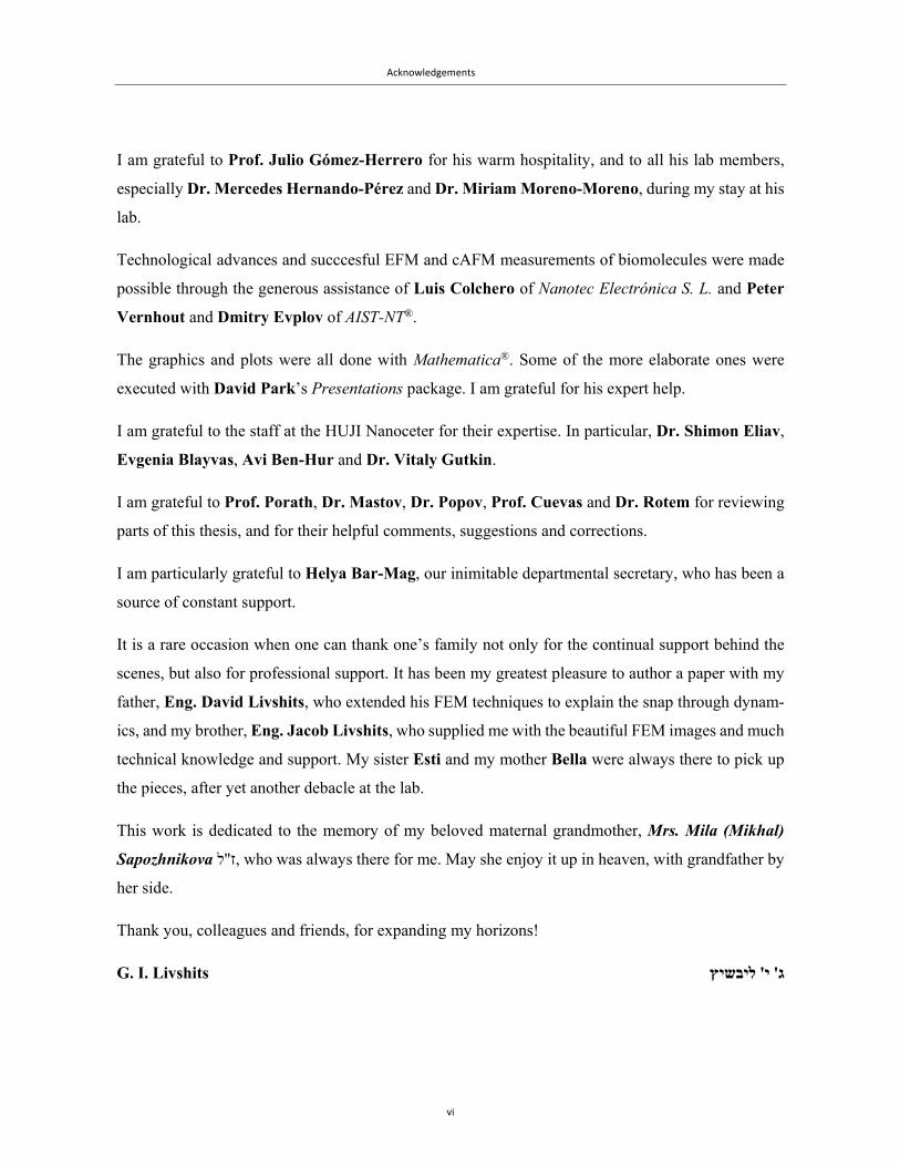
AcknowledgementsIt is a wonderful time, once labour is accomplished, to be able to thank all those the good Lord has
sent to aid me on my scientific journey.
First and foremost is my supervisor, Prof. Danny Porath, who welcomed me to his group with open
arms, and entrusted me with this research project. I could ask for no better supervisor, who gave me
the freedom to tinker around on my own, always with his full financial support and backing.
During the years of my PhD, I was fortunate to work with experts who would become my closest
friends. Such is Dr. Eduard Mastov, whose boundless ingenuity and seasoned professionalism saved
me from many a wrong turn. He has taught me everything I know. Such is Dr. Inna Popov, who
tirelessly worked with me to go beyond the established into the impossible and unknown. Such is
Prof. Juan Carlos Cuevas, who taught me the theoretical aspects of charge transport, always willing
to help, always willing to endure my silly questions. Such is Dr. Igor Brodsky, whose depth of
knowledge inspired me and for whose technical prowess I shall forever be in debt.
I have been a part of a stimulating collective, a group of people with whom I could share my thoughts
and my troubles, amongst whom I count Dr. Jamal Ghabboun, Dr. Errez Shapir, Lev Tal-Or,
Lior Sagiv, Limor Zemel, Dr. Shlomit Greenwald, Dr. Izhar Medalsy, Dr. Hezy Cohen, Dr. Dvir
Rotem, Dr. Yariv Pinto, Dr. Haichao Huang, Roman Zhuravel, Avital Tal, Maya Gottlieb, Iris
Roger-Eitan, Avigail Stern, Abeer Karmi and Guy Koplovitz.
I am particularly grateful to people outside my lab, who supported me, from the sharing of their
professional expertise, to the lending of equipment, through the carrying of heavy loads, to the hours
we have spent in each other’s company. These are Prof. Isaak Lapides, Tal Dagan, Avshalom Ha-
rat and the staff of the Mechanical Workshop, Dr. Natalia Borovok, Gena Eidelshtein, Prof. Sasha
Kotlyar and his lab, Prof. Leonid Gurevich, Prof. Shalom Wind and Erika Penzo, Prof. Spiros
Skourtis, Prof. Rosa DiFelice, Dr. Agostino Migliore, Dr. Rafael Gutierrez, Prof. Micha Asscher
and his lab, Prof. Oded Millo, Prof. Uri Raviv and his lab, Carmen Tamburu, Prof. Sandy Ruh-
man and his lab, Prof. Yehuda Haas and his lab, Prof. Shlomo Magdassi and his lab, Prof. Uri
Banin and his lab, Dr. Itzik Shweky, Dr. Hagai Arbell, Dr. Evgenia Vaganova and Dr. Sasha
Puzenko.
Acknowledgements
vi
I am grateful to Prof. Julio Gómez-Herrero for his warm hospitality, and to all his lab members,
especially Dr. Mercedes Hernando-Pérez and Dr. Miriam Moreno-Moreno, during my stay at his
lab.
Technological advances and succcesful EFM and cAFM measurements of biomolecules were made
possible through the generous assistance of Luis Colchero of Nanotec Electrónica S. L. and Peter
Vernhout and Dmitry Evplov of AIST-NT®.
The graphics and plots were all done with Mathematica®. Some of the more elaborate ones were
executed with David Park’s Presentations package. I am grateful for his expert help.
I am grateful to the staff at the HUJI Nanoceter for their expertise. In particular, Dr. Shimon Eliav,
Evgenia Blayvas, Avi Ben-Hur and Dr. Vitaly Gutkin.
I am grateful to Prof. Porath, Dr. Mastov, Dr. Popov, Prof. Cuevas and Dr. Rotem for reviewing
parts of this thesis, and for their helpful comments, suggestions and corrections.
I am particularly grateful to Helya Bar-Mag, our inimitable departmental secretary, who has been a
source of constant support.
It is a rare occasion when one can thank one’s family not only for the continual support behind the
scenes, but also for professional support. It has been my greatest pleasure to author a paper with my
father, Eng. David Livshits, who extended his FEM techniques to explain the snap through dynam-
ics, and my brother, Eng. Jacob Livshits, who supplied me with the beautiful FEM images and much
technical knowledge and support. My sister Esti and my mother Bella were always there to pick up
the pieces, after yet another debacle at the lab.
This work is dedicated to the memory of my beloved maternal grandmother, Mrs. Mila (Mikhal)
Sapozhnikova ז"ל, who was always there for me. May she enjoy it up in heaven, with grandfather by
her side.
Thank you, colleagues and friends, for expanding my horizons!
G. I. Livshits ג' י' ליבשיץ
vii
AbstractThis dissertation presents an investigation into the electrical properties of two types of G4-DNA
and several DNA-based molecules, targeting them as candidates for molecular wires and devices.
The quest for conductive molecular nanowires for nanoelectronic devices has prompted the
study of the electrical properties of double-stranded (ds)DNA as a prime example of a polymer with
programmable structural versatility1,2. Its structural and electronic properties have inspired its possi-
ble use as a conductive wire, with sufficient delocalization through its π-π stacking to support
transport of charge along the molecule3. This view, however, is simplistic, and does not take into
account the effect of the surroundings on this soft biomolecule4-6. In particular, it is already well-
established that long dsDNA adsorbed on a solid substrate shows no appreciable conduction7-10.
Moreover, the variability in the measured molecules and experimental setups has produced a wide
range of partial or seemingly contradictory results11-14, highlighting the challenge to transport signif-
icant current through individual DNA molecules. In particular, no reproducible and conrolled meas-
urements of charge transport through long individual dsDNA or DNA-based molecules deposited on
a hard substrate have been reported so far.
To address this slew of challenges, we concentrated our studies on a model system, guanine-
based quadruplex DNA (G4-DNA)15-17. The four-stranded configuration forms a quasi-1D structure
with a repeating unit, the tetrad. It is stiffer, compared to dsDNA, and is more likely to withstand
deformations induced by the surface. Its guanine-rich content suggests it is more likely to transport
charge over longer distances18. Two types of G4-DNA were synthesized by our collaborators, tetra-
and intra-molecular G4-DNA, distinguished by the orientation of their constitutive strands. Tetra-
molecular G4-DNA is composed of four single-strands of guanine nucleotides that run parallel to
each other. Each strand is attached to a biotin molecule and four such strands are linked to an avidin
tetramer16. Intra-molecular G4-DNA is obtained by self-folding of a single strand of guanines15,17.
Such folding leads to a pairwise anti-parallel configuration, in which two strands run in one direction
and the other two run in the opposite direction.
Previous work using electrostatic force microscopy (EFM) compared intra-molecular G4-DNA
with long dsDNA19. EFM is a non-contact technique, providing valuable information on the charge
polarization, possibly indicating on charge mobility within a single molecule by measuring its re-
Abstract
viii
sponse to an external electric field induced by an oscillating probe above the molecule. Intra-molec-
ular G4-DNA produced a clear signal of polarizability, whereas dsDNA gave no signal19. In this work,
we wished to go a step further and compare both types of G4-DNA. We found, by atomic force
microscopy (AFM) imaging that – in accordance with our previous work16 – when constructed from
the same number of tetrads, tetra-molecular G4-DNA was thicker and shorter than intra-molecular
G4-DNA16,20. Furthermore, the EFM signal was twice as strong in the parallel configuration as com-
pared with the anti-parallel G4-DNA20. This suggests that the folding orientation of the strands, which
form the backbone, affects the molecular structure, i.e. either the tetrad unit or the tetrad-tetrad π-π
stacking or both, and therefore the charge mobility. Tetra-molecular G4-DNA is more responsive to
the applied field, implying it is a better candidate for charge transport measurements.
These promising results motivated us to perform direct electrical transport measurements on
tetra-molecular G4-DNA. For this purpose, we employed a conductive atomic force microscopy
(cAFM) setup, in which the stationary electrical contact is formed using stencil lithography, while
the conductive tip functions as a second mobile electrode, profiling the conductance along the mole-
cule.
Stencil lithography21 is particularly suited for integrating organic materials into solid-state de-
vices, as it involves no chemical treatment that may damage the sensitive functional element. By
partially covering molecules with a stencil mask, and evaporating metal on top, it is possible to form
robust metal-molecule junctions. Nonetheless, conventional mask patterning techniques suffer from
metal penetration22-24, which adversely affects the molecules. To overcome this limitation, we devel-
oped a specialized technique based on reversible electrostatic clamping of the mask to the substrate.
By utilizing the pull-in instability25,26, we obtained full compliance of the mask to the substrate with
both planar and non-planar geometries27. Our investigations enabled to apply the cAFM technique to
new types of samples and perform measurements on single molecules that were not possible before,
e.g., with symmetric contacts. They have also provided new insight into the clamping dynamics, and
the replica formation and penetration mechanisms27.
We have used this technique in conjunction with cAFM to study different types of molecules:
long dsDNA, tetra-molecular G4-DNA, short segments of single-wall carbon nanotubes (SWCNTs),
multi-wall carbon nanotube (MWCNTs) bundles and networks and SWCNT-dsDNA-SWCNT hybrid
nanostructures.
By contacting a single tetra-molecular G4-DNA molecule at numerous positions along its ex-
posed length, we obtained detailed and consistent current-voltage characteristics (I-Vs), with a non-
Abstract
ix
trivial length dependence, which is compatible with a long-range thermally-activated hopping mech-
anism between multi-tetrad blocks28. Many molecules were measured in this fashion, with currents
of tens to over 100 pA for distances ranging from tens to over 100 nm.
Our unique setup enables reproducible I-V measurements, and as a consequence provides quan-
titative feedback to collaboratoring groups, who synthesize the molecules. New batches of tetra-mo-
lecular G4-DNA showed higher currents over longer distances, e.g. ~350 pA at ~150 nm. Similar
cAFM measurements on long dsDNA showed no conductivity, while short segments of SWCNT
revealed conducting or semi-conducting characteristics, commensurate with the known properties of
these molecules. Preliminary measurements on a few short dsDNA (26 bp) between two SWCNTs
revealed a great variability, attributed to the different configurations of the hybrid structures.
Methods and Major Findings 1. AFM and EFM comparison of co-deposited tetra- and intra-molecular G4-DNA reveals
variations in morphology and different sensitivity to the applied field, suggesting that the
folding orientation of the strands affects both the molecular structure, i.e. either the tetrad
unit or the tetrad-tetrad stacking or both, and therefore the charge mobility.
2. Tetra-molecular G4-DNA is twice as polarizable as intra-molecular G4-DNA, suggesting
it has greater charge mobility.
3. Reproducible currents of tens to over 100 pA were measured in many tetra-molecular G4-
DNA molecules over distances ranging from tens to over 100 nm. The measured charge
transport is compatible with long-range thermally activated hopping between multi-tetrad
segments.
4. A new variant of the stencil lithography method was developed, based on reversible elec-
trostatic clamping, overcoming indeterminate blurring effects associated with the problem
of metal penetration in standard mask patterning techniques. This method enabled to
demonstrate full mask compliance in scanning electron microscopy (SEM) and AFM
measurements. The pull-in instability was demonstrated inside an SEM chamber and was
confirmed by a non-linear transient response computation.
5. The above technique enabled to prepare new samples, which enabled measurements that
were not possible before, including cAFM with symmetric evaporated contacts on indi-
vidual SWCNTs.
Abstract
x
6. New mechanisms were proposed for the replica formation and the blurring effect based
on cluster evaporation and mobile source decay, explaining the ultimate resolution of the
masking technique and its limitations.
References
1 Seeman, N. C. DNA in a material world. Nature 421, 427‐431 (2003). 2 Seeman, N. C. An overview of structural DNA Nanotechnology. Mol Biotechnol 37, 246‐257 (2007). 3 Bixon, M. et al. Long‐range charge hopping in DNA. P Natl Acad Sci USA 96, 11713‐11716 (1999). 4 Heim, T., Deresmes, D. & Vuillaume, D. Conductivity of DNA probed by conducting‐atomic force microscopy:
Effects of contact electrode, DNA structure, and surface interactions. J Appl Phys 96, 2927‐2936 (2004). 5 Gutierrez, R., Porath, D. & Cuniberti, G. in Charge Transport in Disorderd Solids with Applications in Electron‐
ics (ed Sergei Baranovski) (Wiley, 2006). 6 Cai, L. T., Tabata, H. & Kawai, T. Probing electrical properties of oriented DNA by conducting atomic force mi‐
croscopy. Nanotechnology 12, 211‐216 (2001). 7 Storm, A. J., van Noort, J., de Vries, S. & Dekker, C. Insulating behavior for DNA molecules between nanoelec‐
trodes at the 100 nm length scale. Appl Phys Lett 79, 3881‐3883 (2001). 8 de Pablo, P. J. et al. Absence of dc‐conductivity in lambda‐DNA. Phys Rev Lett 85, 4992‐4995 (2000). 9 Bockrath, M. et al. Scanned conductance microscopy of carbon nanotubes and lambda‐DNA. Nano Lett 2,
187‐190 (2002). 10 Braun, E., Eichen, Y., Sivan, U. & Ben‐Yoseph, G. DNA‐templated assembly and electrode attachment of a con‐
ducting silver wire. Nature 391, 775‐778 (1998). 11 Astakhova, T. Y., Likhachev, V. N. & Vinogradov, G. A. Long‐range charge transfer in biopolymers. Russ Chem
Rev+ 81, 994‐1010 (2012). 12 Endres, R. G., Cox, D. L. & Singh, R. R. P. Colloquium: The quest for high‐conductance DNA. Rev Mod Phys 76,
195‐214 (2004). 13 Porath, D., Cuniberti, G. & Di Felice, R. Charge transport in DNA‐based devices. Top Curr Chem 237, 183‐227
(2004). 14 Muren, N. B., Olmon, E. D. & Barton, J. K. Solution, surface, and single molecule platforms for the study of
DNA‐mediated charge transport. Phys Chem Chem Phys 14, 13754‐13771 (2012). 15 Borovok, N., Molotsky, T., Ghabboun, J., Porath, D. & Kotlyar, A. Efficient procedure of preparation and prop‐
erties of long uniform G4‐DNA nanowires. Anal Biochem 374, 71‐78 (2008). 16 Borovok, N. et al. Assembling of G‐strands into novel tetra‐molecular parallel G4‐DNA nanostructures using
avidinbiotin recognition. Nucleic Acids Res 36, 5050‐5060 (2008). 17 Kotlyar, A. B. et al. Long, monomolecular guanine‐based nanowires. Adv Mater 17, 1901‐1904 (2005). 18 Calzolari, A., Di Felice, R., Molinari, E. & Garbesi, A. G‐quartet biomolecular nanowires. Appl Phys Lett 80,
3331‐3333 (2002). 19 Cohen, H. et al. Polarizability of G4‐DNA observed by electrostatic force microscopy measurements. Nano
Lett 7, 981‐986 (2007). 20 Livshits, G. I., Ghabboun, J., Borovok, N., Kotlyar, A. & Porath, D. Comparative EFM of mono‐ and tetra‐molec‐
ular G4‐DNA. Adv Mater 26, 4981‐4985 (2014). 21 Deshmukh, M. M., Ralph, D. C., Thomas, M. & Silcox, J. Nanofabrication using a stencil mask. Appl Phys Lett
75, 1631‐1633 (1999). 22 Vazquez‐Mena, O. et al. Analysis of the blurring in stencil lithography. Nanotechnology 20, 415303 (2009). 23 Podzorov, V., Sysoev, S. E., Loginova, E., Pudalov, V. M. & Gershenson, M. E. Single‐crystal organic field effect
transistors with the hole mobility similar to 8 cm(2)/V s. Appl Phys Lett 83, 3504‐3506 (2003). 24 Racz, Z. & Seabaugh, A. Characterization and control of unconfined lateral diffusion under stencil masks. J Vac
Sci Technol B 25, 857‐861 (2007). 25 Rebeiz, G. M. RF MEMS: Theory, Design and Technology. (John Wiley & Sons, 2003). 26 Senturia, S. D. Microsystem Design. (Kluwer Academic Pulishers, 2002). 27 Livshits, G. I. et al. Chemical‐free lithography with nanometer‐precision via reversible electrostatic clamping.
(2014). 28 Livshits, G. I. et al. Long‐range charge transport in single G‐quadruplex DNA molecules. Nat Nanotechnol In
Press (2014).
xi
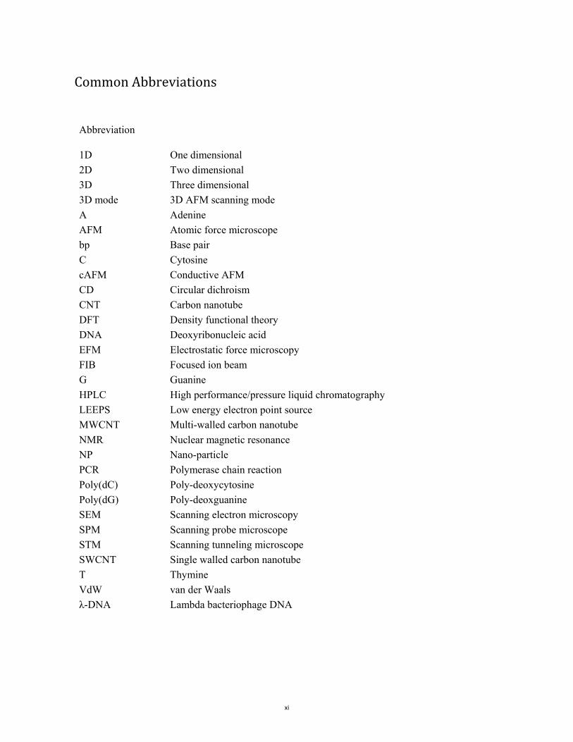
CommonAbbreviations
Abbreviation
1D One dimensional
2D Two dimensional
3D Three dimensional
3D mode 3D AFM scanning mode
A Adenine
AFM Atomic force microscope
bp Base pair
C Cytosine
cAFM Conductive AFM
CD Circular dichroism
CNT Carbon nanotube
DFT Density functional theory
DNA Deoxyribonucleic acid
EFM Electrostatic force microscopy
FIB Focused ion beam
G Guanine
HPLC High performance/pressure liquid chromatography
LEEPS Low energy electron point source
MWCNT Multi-walled carbon nanotube
NMR Nuclear magnetic resonance
NP Nano-particle
PCR Polymerase chain reaction
Poly(dC) Poly-deoxycytosine
Poly(dG) Poly-deoxguanine
SEM Scanning electron microscopy
SPM Scanning probe microscope
STM Scanning tunneling microscope
SWCNT Single walled carbon nanotube
T Thymine
VdW van der Waals
λ-DNA Lambda bacteriophage DNA
12
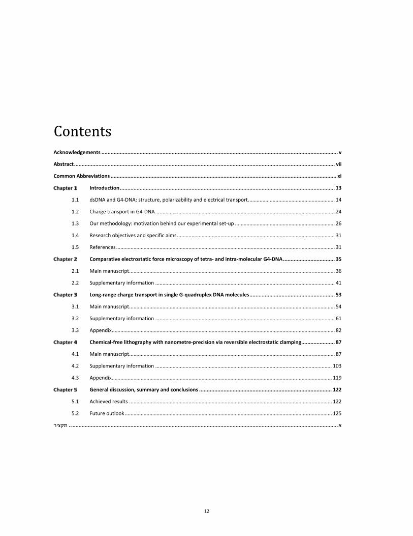
ContentsAcknowledgements ........................................................................................................................................................... v
Abstract ........................................................................................................................................................................... vii
Common Abbreviations .................................................................................................................................................... xi
Introduction ............................................................................................................................................. 13
1.1 dsDNA and G4‐DNA: structure, polarizability and electrical transport ............................................................ 14
1.2 Charge transport in G4‐DNA ............................................................................................................................ 24
1.3 Our methodology: motivation behind our experimental set‐up ..................................................................... 26
1.4 Research objectives and specific aims ............................................................................................................. 31
1.5 References ....................................................................................................................................................... 31
Comparative electrostatic force microscopy of tetra‐ and intra‐molecular G4‐DNA .................................. 35
2.1 Main manuscript .............................................................................................................................................. 36
2.2 Supplementary information ............................................................................................................................ 41
Long‐range charge transport in single G‐quadruplex DNA molecules ........................................................ 53
3.1 Main manuscript .............................................................................................................................................. 54
3.2 Supplementary information ............................................................................................................................ 61
3.3 Appendix .......................................................................................................................................................... 82
Chemical‐free lithography with nanometre‐precision via reversible electrostatic clamping ...................... 87
4.1 Main manuscript .............................................................................................................................................. 87
4.2 Supplementary information .......................................................................................................................... 103
4.3 Appendix ........................................................................................................................................................ 119
General discussion, summary and conclusions ....................................................................................... 122
5.1 Achieved results ............................................................................................................................................ 122
5.2 Future outlook ............................................................................................................................................... 125
א .............................................................................................................................................................................. .. תקציר
13
IntroductionMore than sixty years have elapsed since the discovery of the structure of double-stranded (ds)DNA1.
Nearly thirty years have passed since the discovery of the polymerase chain reaction (PCR)2, and then
almost a decade for it to become programmable and automatic, one of the main tools of biochemists,
molecular biologists and geneticists. These giant discoveries were centred on large assemblies of
molecules, from the crystallization of dsDNA for X-ray analysis to the complex enzymatic reactions
of biomolecules. Finally, the tide has shifted somewhat, and the scientific world is beginning to work
with individual biomolecules, trying to measure their idiosyncratic characteristics to reveal their vital
information. After some twenty years of foray, fuelled largely by the invention of scanning probe
microscopy3,4, it is now possible to routinely and innocuously image individual molecules, discern
their shape, measure their thermodynamic properties and even visualize their constitutive elements.
This is the dawn of single molecule science, and the present work is part of this effort, to elucidate
the characteristics of individual guanine (G) quadruplex DNA molecules (G4-DNA), and to go be-
yond their morphological properties to measure electrostatic polarizability and long-range charge
transport.
This work, encompassing three papers, describes an investigation of the electrical properties of indi-
vidual G4-DNA molecules. In this Introduction, the important experiments in this field are surveyed,
with special attention to previous experiments with G4-DNA, concentrating on its morphology, elec-
trostatic polarizability and electrical conductivity. The theoretical aspects of charge transport in this
molecule are briefly discussed, and the motivation behind our experimental set-up is provided. In
Chapter 2, the results of a comparative electrostatic force microscopy (EFM) study of two forms of
G4-DNA are presented, demonstrating that the orientation of the constitutive strands affects morphol-
ogy, which in turn affects the response to an external electric field. In Chapter 3, the current-voltage
characteristics of G4-DNA, measured using a method developed especially for this purpose, are pre-
sented, demonstrating long-range charge transport compatible with a thermally-activated hopping
mechanism in this completely organic 1D polymer adsorbed on a mica substrate. In Chapter 4, a
method for the formation of reliable, reproducible and well-defined contact leads to individual bio-
molecules is presented. This method is discussed in detail, and new mechanisms for the formation of
the boundary and the penetration are presented. Finally, the summary of the work and a future outlook
Introduction
14
are presented in Chapter 5. In addition to the conclusions from the three papers, the summary also
provides complementary insight into the work. Since this thesis is presented as a collection of papers,
each chapter contains its own bibliography.
1.1 dsDNAandG4‐DNA:structure,polarizabilityandelectricaltransport
DNA, with its structural versatility through its self-assembly and molecular recognition capabilities,
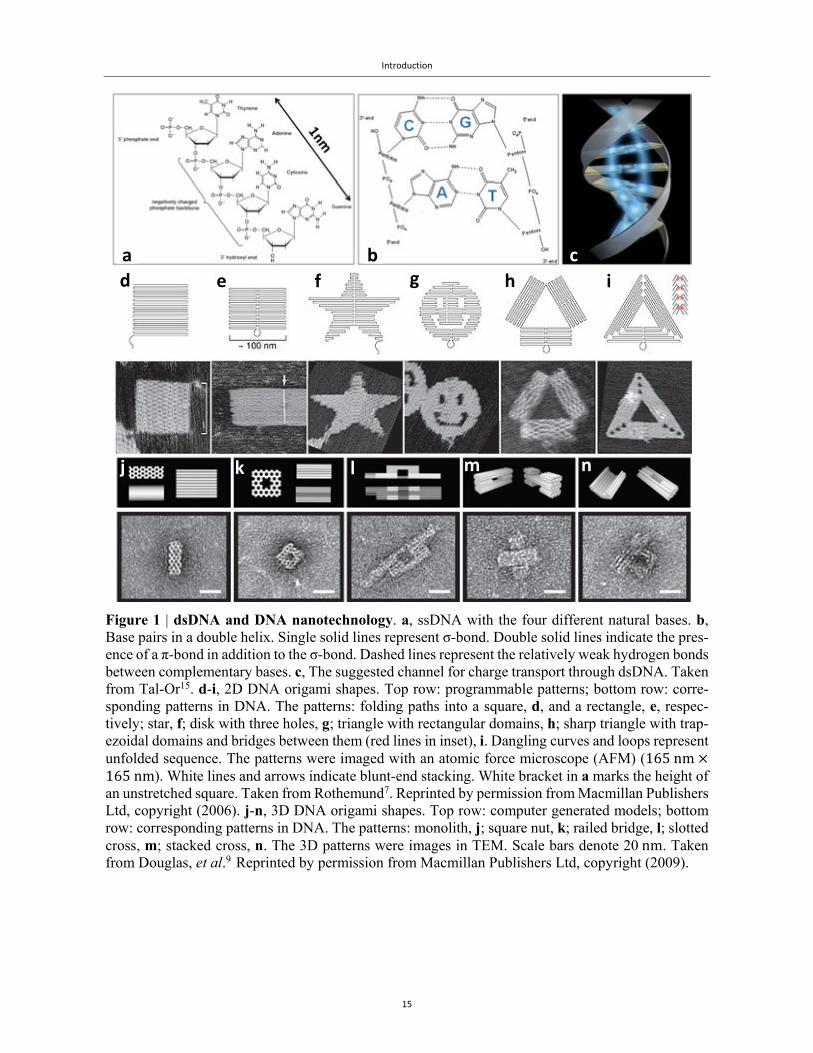
is at the centre of bio-nanotechnology5-10. Fig. 1 shows several facets of this rich mosaic. Figs. 1a-1c
show a scheme of dsDNA with its four constitutive bases and double-helical structure. A few cele-
brated 2D and 3D patterns made with DNA technology, called "DNA origami", are given in Figs. 1d-
1i and Figs. 1j-1n, respectively, demonstrating but a fraction of the boundless richness of the DNA
motif.
Moreover, it has already been suggested since the early 1960s that charge carriers moving along DNA
strands played an important role in the repair mechanisms of dsDNA, with the π-stacked electronic
structure of the bases serving as the main conduction channel for the charge carriers11 (Fig. 1c). This
could have meant that dsDNA was not only structurally versatile, but also electrically conductive.
In the early 1970s, Aviram and Ratner proposed the (theoretical) construction of a molecular diode12
from a generic donor-acceptor complex, sparking the field of molecular electronics. Along with the
debates over the charge transfer mechanism in dsDNA13 and dsDNA's ability to transport charge14,
these became the major incentive behind the investigations into the use of DNA as a programmable
electrical conduit for the microelectronics industry. This industry is facing new challenges in the form
of quantum correlation effects as it continues to shrink the circuitry to the range of tens of nanometres,
and the idea, in the early days of nanotechnology, was to replace some circuit elements with conduc-
tive wires or molecules. In this sense, dsDNA seemed very promising as a genuine example of a one-
dimensional programmable polymer with electrical mobility.
Introduction
15
Figure 1 | dsDNA and DNA nanotechnology. a, ssDNA with the four different natural bases. b, Base pairs in a double helix. Single solid lines represent σ-bond. Double solid lines indicate the pres-ence of a π-bond in addition to the σ-bond. Dashed lines represent the relatively weak hydrogen bonds between complementary bases. c, The suggested channel for charge transport through dsDNA. Taken from Tal-Or15. d-i, 2D DNA origami shapes. Top row: programmable patterns; bottom row: corre-sponding patterns in DNA. The patterns: folding paths into a square, d, and a rectangle, e, respec-tively; star, f; disk with three holes, g; triangle with rectangular domains, h; sharp triangle with trap-ezoidal domains and bridges between them (red lines in inset), i. Dangling curves and loops represent unfolded sequence. The patterns were imaged with an atomic force microscope (AFM) (165nm165nm). White lines and arrows indicate blunt-end stacking. White bracket in a marks the height of an unstretched square. Taken from Rothemund7. Reprinted by permission from Macmillan Publishers Ltd, copyright (2006). j-n, 3D DNA origami shapes. Top row: computer generated models; bottom row: corresponding patterns in DNA. The patterns: monolith, j; square nut, k; railed bridge, l; slotted cross, m; stacked cross, n. The 3D patterns were images in TEM. Scale bars denote 20nm. Taken from Douglas, et al.9 Reprinted by permission from Macmillan Publishers Ltd, copyright (2009).
c a b
j k l m n
d e f g h i
Introduction
16
With a substantial boom around the turn of the century, the number of reported direct experimental
observations of charge transport in individual dsDNA molecules and DNA-based derivatives has been
in decline in the past few years, quite possibly a reflection of the formidable challenge involved in
such experiments. A few notable experiments, directly related to the present work, demonstrating the
state-of-the-art are briefly reviewed below. A more thorough treatment of the subject is found in
recent reviews by Astakhova et al.16 and Muren et al.17 See also Enders et al.18 and Porath et al.19,20
for a survey of the early experiments.
Electronic and electrical data21,22, accumulated over the past two decades, have made it clear that
individual biomolecules exhibit great variance among themselves23. This variance is compounded by
their fragile nature, and the difficulty to form well-defined electrical contacts. Unlike sturdy metal
wires and carbon nanotubes (CNTs), molecules of biological origin are particularly susceptible to
external factors, which have a major impact on these molecules by influencing their conformation,
especially through their non-specific binding to a hard surface24 and the accumulation of defects along
their length. These, in turn, have negatively affected, and often unpredictably so, the electrical prop-
erties of the molecule. As a case in point, we note that despite the initial sanguine theoretical predic-
tions25, individual molecules of long dsDNA (over 40 nm) adsorbed on a hard substrate have shown
virtually no conductivity in dry conditions26-28, or ionic conductivity based on high humidity, in which
the hydration layer acts as the electrical pathway29,30. These results, confirmed by several groups31-33
as well as by our own measurements (see Chapter 3), meant long dsDNA was a poor electrical con-
ductor by itself, quite possibly due to defects induced by its attachment to the substrate.
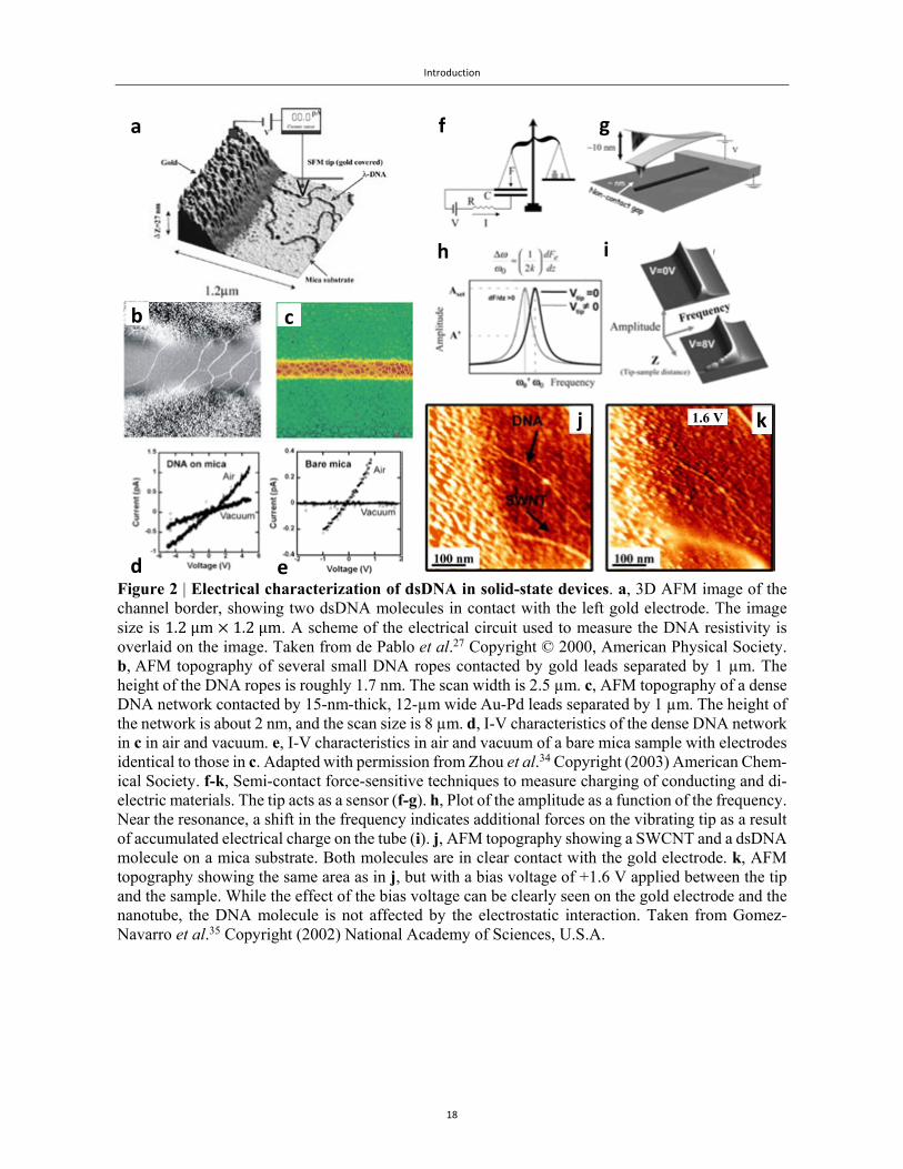
Fig. 2 shows a collection of selected results from the published literature on electrical measurements
of dsDNA adsorbed on a hard substrate. These results can be categorized through their electrical
contact to the molecule. In the left column (Figs. 2a-2e), we have two illustrative examples of direct
contact. Fig. 2a is an early example of a conductive atomic force microscope (cAFM) setup. Typi-
cally, this setup is composed of a stationary contact (evaporated electrode) and a mobile contact (met-
allized tip), making it possible to sample the current-voltage characteristics along the length of the
molecule. In this case, de Pablo et al.27 had measured individual dsDNA molecules that were found
protruding from under the evaporated contact, and have concluded they were not electrically conduc-
tive. On the other hand, Zhou et al.34 investigated networks of dsDNA bundles and molecules, as
shown in Figs. 2b-2c. They used two stationary evaporated contacts. Their current-voltage data (Figs.
2d-2e) also point to very low currents (~1 pA), which are sensitive to ambient humidity.
Introduction
17
Figs. 2f-2k in the right column illustrate a different approach, based on force measurements. This
technique complements the direct contact method, and provides indications on charge mobility within
the molecule. In those experiments, a potential difference was applied between the molecule and the
cAFM tip (Figs. 2f-2g). From an electrostatic point of view, any molecular wire can be modelled as
a resistance and a capacitance. In this situation, the wire is electrically connected to the electrode, so
that charge passing through the resistor charges the capacitor. Gomez-Narravo et al.35 have used this
setup in the following way. They realized that the amount of charge in the capacitor could be meas-
ured by placing the force detector (tip) over the molecule. The tip is oscillated at its resonance fre-
quency, and the amplitude of the oscillation is monitored and kept constant. The electrostatic force
gradient between the tip and the molecule induces a shift in the resonance frequency, as shown in
Figs. 2h-2i. If no frequency shift is observed over the molecule, one can conclude that no charge has
passed through the molecule and therefore it is an insulator. This principle is clearly demonstrated in
Figs. 2j-2k, where a single-wall carbon nanotube (SWCNT) and a dsDNA molecule are observed
protruding from under the border. Fig. 2j is an AFM topography of the border, while Fig. 2k is the
same but with a potential difference of +1.6 V between the tip and the substrate. As a result, both the
gold electrode and the SWCNT that is electrically connected to it appear wider and higher (brighter)
because of the electrostatic interaction, whereas no change is observed in the dsDNA molecule, indi-
cating it is an insulator.
Introduction
18
Figure 2 | Electrical characterization of dsDNA in solid-state devices. a, 3D AFM image of the channel border, showing two dsDNA molecules in contact with the left gold electrode. The image size is 1.2μm 1.2μm. A scheme of the electrical circuit used to measure the DNA resistivity is overlaid on the image. Taken from de Pablo et al.27 Copyright © 2000, American Physical Society. b, AFM topography of several small DNA ropes contacted by gold leads separated by 1 µm. The height of the DNA ropes is roughly 1.7 nm. The scan width is 2.5 µm. c, AFM topography of a dense DNA network contacted by 15-nm-thick, 12-µm wide Au-Pd leads separated by 1 µm. The height of the network is about 2 nm, and the scan size is 8 µm. d, I-V characteristics of the dense DNA network in c in air and vacuum. e, I-V characteristics in air and vacuum of a bare mica sample with electrodes identical to those in c. Adapted with permission from Zhou et al.34 Copyright (2003) American Chem-ical Society. f-k, Semi-contact force-sensitive techniques to measure charging of conducting and di-electric materials. The tip acts as a sensor (f-g). h, Plot of the amplitude as a function of the frequency. Near the resonance, a shift in the frequency indicates additional forces on the vibrating tip as a result of accumulated electrical charge on the tube (i). j, AFM topography showing a SWCNT and a dsDNA molecule on a mica substrate. Both molecules are in clear contact with the gold electrode. k, AFM topography showing the same area as in j, but with a bias voltage of +1.6 V applied between the tip and the sample. While the effect of the bias voltage can be clearly seen on the gold electrode and the nanotube, the DNA molecule is not affected by the electrostatic interaction. Taken from Gomez-Navarro et al.35 Copyright (2002) National Academy of Sciences, U.S.A.
a
e
b c
d
f g
h i
1.6 V j k
Introduction
19
From the transport measurements on dsDNA in the last 15 years the following picture emerges: (i)
charge transport is blocked for long (over 40 nm) single dsDNA molecules attached to surfaces; (ii)
charge can be transported along short and single dsDNA molecules detached from the substrate (in
either suspended or standing configurations36-40); (iii) conductance strongly depends on the charge
injection efficiency at the molecule-electrode contact; (iv) charge transport depends on the dsDNA
sequence; and (v) charge transport depends on the environment (solvent/ambient/vacuum, tempera-
ture, gate, etc.).
This picture implies that a radical approach would be required to enable long-range charge transport
in the solid-state setting, which is the more relevant configuration for the electronics industry. Most
researchers in the field of single-molecule science had abandoned all together this quest, and have
concentrated on experiments in which dsDNA functioned as a template or scaffold for other conduc-
tive species, such as polyaniline41,42 and metallic intercalators and coatings43,44. Our group did not
give up; rather, we have opted to search for completely organic derivatives of DNA that would be
able to withstand the vicissitudes of deposition, fabrication and measurement. In this respect, the
molecular object of this thesis, guanine-based quadruplex DNA, or G4-DNA for short, has been a
promising candidate ever since it was observed to be less affected by surface interactions (through
measurements of its relatively long persistence length (~100 nm) and considerable apparent height45)
and to have a measurable electrostatic polarizability46-48 (see below).
G4-DNA was discovered over fifty years ago when it was correctly identified as the unexpected
product of a reaction meant originally to synthesize polyguanylic acid, but in fact its origins lie in the
early 1900s! A recent book, edited by Fritzsche and Spindler49, contains a survey of the history of the
field, along with contributions from leading scientists with recent results and discoveries. See also
the review by Davies50. Here we briefly describe the relevant information, and collect the pertinent
results.
Introduction
20
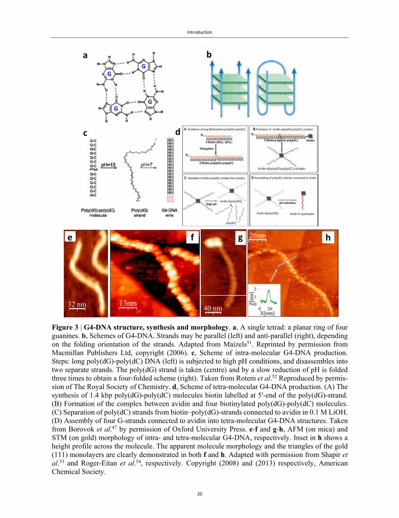
Figure 3 | G4-DNA structure, synthesis and morphology. a, A single tetrad: a planar ring of four guanines. b, Schemes of G4-DNA. Strands may be parallel (left) and anti-parallel (right), depending on the folding orientation of the strands. Adapted from Maizels51. Reprinted by permission from Macmillan Publishers Ltd, copyright (2006). c, Scheme of intra-molecular G4-DNA production. Steps: long poly(dG)-poly(dC) DNA (left) is subjected to high pH conditions, and disassembles into two separate strands. The poly(dG) strand is taken (centre) and by a slow reduction of pH is folded three times to obtain a four-folded scheme (right). Taken from Rotem et al.52 Reproduced by permis-sion of The Royal Society of Chemistry. d, Scheme of tetra-molecular G4-DNA production. (A) The synthesis of 1.4 kbp poly(dG)-poly(dC) molecules biotin labelled at 5′-end of the poly(dG)-strand. (B) Formation of the complex between avidin and four biotinylated poly(dG)-poly(dC) molecules. (C) Separation of poly(dC) strands from biotin–poly(dG)-strands connected to avidin in 0.1 M LiOH. (D) Assembly of four G-strands connected to avidin into tetra-molecular G4-DNA structures. Taken from Borovok et al.47 by permission of Oxford University Press. e-f and g-h, AFM (on mica) and STM (on gold) morphology of intra- and tetra-molecular G4-DNA, respectively. Inset in h shows a height profile across the molecule. The apparent molecule morphology and the triangles of the gold (111) monolayers are clearly demonstrated in both f and h. Adapted with permission from Shapir et al.53 and Roger-Eitan et al.54, respectively. Copyright (2008) and (2013) respectively, American Chemical Society.
40 nm
a b
c d
g
GG
GG
h f e
32 nm
Introduction
21
Fig. 3 shows the structural attributes of G4-DNA. G4-DNA is composed of a large number of stacked
guanine tetrads (also known as quartets), with each tetrad constructed out of four guanine bases form-
ing a planar square (Fig. 3a). Structurally, each tetrad is held by eight Hoogsteen-type hydrogen
bonds, giving in average two bonds to each base, instead of the two or three hydrogen bonds between
A-T and G-C in the dsDNA (Fig. 1b), respectively, which on average produce one or one and a half
hydrogen bonds per base, respectively. The tetrads are stacked together in a helical arrangement (Fig.
3b), with a stacking distance and twist angle, 3.25 Å and 30°, respectively, that are smaller than the
corresponding values in dsDNA55, implying improved π-π overlap along the stacking direction of G4-
DNA, as is also found in DFT calculations56 (see also Chapter 2). Different conformation and folding
orientations of these long strands are possible, such as a parallel or tetra-molecular G4-DNA (Fig. 3b,
left) and the pairwise anti-parallel or intra-molecular G4-DNA (Fig. 3b, right).
Short G4-DNA fragments can be spontaneously assembled into long G4-DNA, but the resulting wires
are non-uniform with gaps between the fragments57-59. Prof. Kotlyar and his group at Tel Aviv Uni-
versity have developed novel synthesis methods to overcome this limitation. Our group has been
working in close collaboration with Prof. Kotlyar with imaging and electrical characterization capa-
bilities. In 2005 (and later in 2008), a joint study reported the synthesis of long intra-molecular G4-
DNA45,60, which was produced from parent poly(dG)-poly(dC) molecules, as shown in Fig. 3c. These
molecules were separated into the poly(dG) and poly(dC) strands at high pH. These strands were
isolated from each other by high-pressure liquid chromatography (HPLC). The pH of the poly(dG)
solution was then slowly reduced to 7. As a result, the molecules were folded into intra-molecular
wires, with a pairwise antiparallel orientation of the four strands (Fig. 3b, right), as demonstrated by
adsorption and circular dichroism (CD) spectra and by AFM45,60 and STM53 imaging.
These wires were further stabilized in the presence of metal cations (K+, Na+). Whereas metal cations
are considered essential for the stability of short G4-DNA molecules (since their positive charge re-
duces the electrostatic repulsion between the stacked tetrads due to the negatively charged phosphate
groups in the nucleotides), it is important to note that long intra-molecular G4-DNA wires were also
stable in the absence of such metal cations. It is likely that the collective stabilization of the π-π
stacking along the long molecules is sufficient to keep them together.
In 2008, our groups reported the synthesis of tetra-molecular G4-DNA47 wires (Fig. 3b, left). These
wires were stable in the absence of metal cations. The basic idea behind the synthesis was to use of
the avidin-tetramer in order to assemble four single strands of guanine, which were each attached to
a biotin at the 5' position. Avidin is a glycoprotein, consisting of four identical subunits, each capable
Introduction
22
of binding tightly a biotin molecule61. The synthesis, depicted schematically in Fig. 3d, consisted of
four main stages. In the first step, 5'-biotinylated-poly(dG)-poly(dC) molecules were synthesized.
Later, a complex between the avidin and four biotinylated poly(dG)-poly(dC) molecules was formed.
Next, the poly(dC) strands were separated from the poly(dG)-strands connected to the avidin in high
pH conditions. The fraction of the four G-strands connected to avidin was purified using size-exclu-
sion HPLC. In the final stage, after the pH was reduced, the four G-strands connected to avidin were
assembled into tetra-molecular G4-DNA structures. The surface morphology of these structures was
characterized by AFM47 and STM54 imaging. AFM imaging showed each molecule was composed
of a linear segment corresponding to the DNA and a brighter (higher) sphere corresponding to the
avidin (Fig. 3g).
High-resolution STM scans (Figs. 3f and 3h) demonstrate the clear periodic structure of both intra-
and tetra-molecular G4-DNA53,54, with bulbs corresponding to the helix pitch with an average length
of ~3.5 nm in both cases. Interestingly, even though they display different height when adsorbed on
a mica substrate, on a gold substrate both types have a similar height, ~1.5 nm.
To study the polarizability of these long G4-DNA wires, our group has used electrostatic force mi-
croscopy (EFM)62. EFM is, in fact, a variation of the technique described in Figs. 2f-2k, except that
the molecule is not connected to an electrode, so charging is not possible. Instead, a potential differ-
ence is applied between the metallized tip and a metallic holder under the substrate, and the tip is
lifted above the set-point, beyond the range of dispersive interactions, to a distance from the substrate
where electrostatic interactions are dominant. For small amplitudes, in the linear feedback regime,
the phase shift, much like the frequency shift in Fig. 2h, is proportional to the gradient of the forces62.
This way we can obtain both a topographical image (at set-point height) and a phase-shift image at a
pre-defined height above the set-point. This is called retrace or plane mode. Different variations of
this technique exist, collectively labelled ‘3D modes’. The changes in amplitude were compensated
during the actual retrace, such that the actual lift of the tip at its lower position was monitored. Using
this technique, we obtained valuable information on the polarizability of G4-DNA as shown in Fig.
4. Intra-molecular G4-DNA was compared to dsDNA (Fig. 4, top panel), and was shown to yield a
signal of polarizability, while dsDNA produced no signal. Tetra-molecular G4-DNA was also shown
to possess a distinct signal of polarizability (Fig. 4, bottom two panels). EFM is explained in detail in
Chapter 2.
Introduction
23
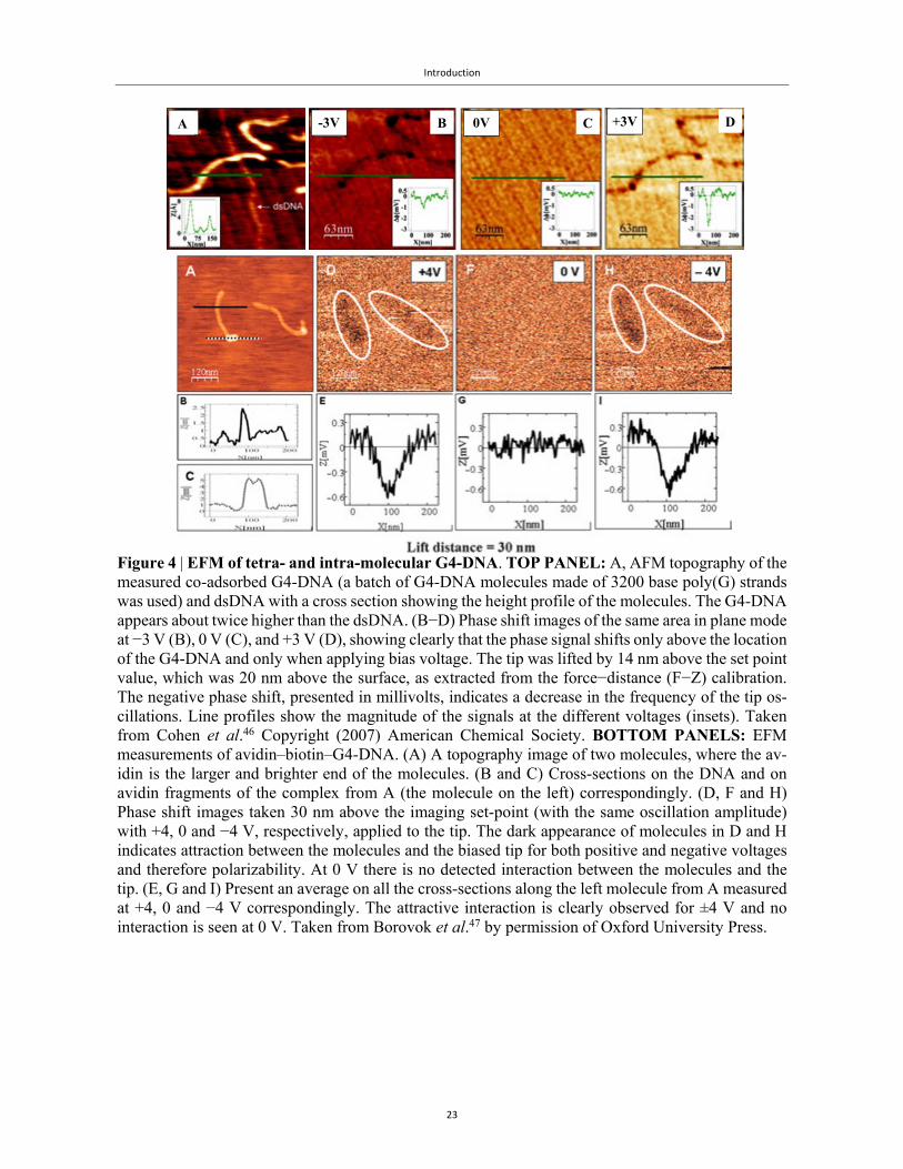
Figure 4 | EFM of tetra- and intra-molecular G4-DNA. TOP PANEL: A, AFM topography of the measured co-adsorbed G4-DNA (a batch of G4-DNA molecules made of 3200 base poly(G) strands was used) and dsDNA with a cross section showing the height profile of the molecules. The G4-DNA appears about twice higher than the dsDNA. (B−D) Phase shift images of the same area in plane mode at −3 V (B), 0 V (C), and +3 V (D), showing clearly that the phase signal shifts only above the location of the G4-DNA and only when applying bias voltage. The tip was lifted by 14 nm above the set point value, which was 20 nm above the surface, as extracted from the force−distance (F−Z) calibration. The negative phase shift, presented in millivolts, indicates a decrease in the frequency of the tip os-cillations. Line profiles show the magnitude of the signals at the different voltages (insets). Taken from Cohen et al.46 Copyright (2007) American Chemical Society. BOTTOM PANELS: EFM measurements of avidin–biotin–G4-DNA. (A) A topography image of two molecules, where the av-idin is the larger and brighter end of the molecules. (B and C) Cross-sections on the DNA and on avidin fragments of the complex from A (the molecule on the left) correspondingly. (D, F and H) Phase shift images taken 30 nm above the imaging set-point (with the same oscillation amplitude) with +4, 0 and −4 V, respectively, applied to the tip. The dark appearance of molecules in D and H indicates attraction between the molecules and the biased tip for both positive and negative voltages and therefore polarizability. At 0 V there is no detected interaction between the molecules and the tip. (E, G and I) Present an average on all the cross-sections along the left molecule from A measured at +4, 0 and −4 V correspondingly. The attractive interaction is clearly observed for ±4 V and no interaction is seen at 0 V. Taken from Borovok et al.47 by permission of Oxford University Press.
-3V 0V +3V A B C D
Introduction
24
1.2 ChargetransportinG4‐DNA
There are several advantages to G4-DNA. As we mentioned above, it is four-stranded and more
tightly packed, so the π-π overlap is greater, compared to dsDNA. Certainly its improved stiffness is
commendable, and may well be the reason for its polarizability on a mica substrate. The attachment
to the substrate influences its conformation, and therefore its structural attributes must be vital to its
success as a true molecular wire.
All the reported non-contact measurements suggest that structural, electronic and electrical properties
are intertwined in these types of molecules. In this respect, the real success of G4-DNA over dsDNA
lies in four inter-related facts. The first is that the guanine bases are known to have the lowest oxida-
tion potential among the DNA bases, thus promoting more efficient charge migration along the mol-
ecule50. The second is the fact that it is a highly ordered structure. Although it is a polymer, it is
structured in a way that is reminiscent of crystals, and the more order a structure has, the greater the
possibility to conduct electricity. Thirdly, although G4-DNA is structurally more stable than dsDNA,
Woiczikowski et al.63 suggest that the potential improvement of its electrical transport properties is
not necessarily related to an increased stability, but rather to the fact that G4-DNA is able to explore
in its conformational space a larger number of charge-transfer active conformations between the
strands. This means that charge, flowing through the molecule, has several pathways. If one of them
is blocked, then the improved coupling between them allows the charge to explore other paths through
a hopping mechanism. Finally, the improved structural stability of G4-DNA does become crucial
once the molecule is contacted by electrodes. In this case, G4-DNA may experience weaker structural
distortions than dsDNA and thus preserve to a higher degree its conduction properties63. The theoret-
ical aspects of charge transport in G4-DNA are explored extensively in Chapter 3.
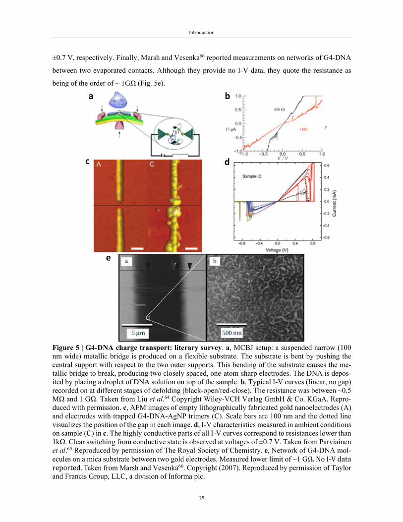
To date, three experiments have been published on G4-DNA conductivity. Liu et al.64 have used the
mechanical break junction (MCBJ) technique to investigate the transport in short (3-tetrad long) G4-
DNA sequences covalently bound between two gold electrodes, as illustrated in Fig. 5a. They meas-
ured high currents (Fig. 5b) that depended on the folding of the molecule, through the opening and
closing of the gap. Parviainen et al.65 have used dielectrophoretic trapping to study the conductivity
of G4-DNA silver nanoparticle structures (Fig. 5c). These structures were composed of three 20 nm
silver nanoparticles connected to each other by means of 20 tetrad G4-DNA linkers. They observed
reversible switching in the conduction. In the range from –0.7 V to +0.7 V they measured linear I-V
curves with a resistance R~1kΩ, while above 0.7 V or below -0.7 V, no current was observed (Fig.
5d). This reversibility has been attributed to oxidation and reduction of guanine bases at potentials of
Introduction
25
±0.7 V, respectively. Finally, Marsh and Vesenka66 reported measurements on networks of G4-DNA
between two evaporated contacts. Although they provide no I-V data, they quote the resistance as
being of the order of ~ 1GΩ (Fig. 5e).
Figure 5 | G4-DNA charge transport: literary survey. a, MCBJ setup: a suspended narrow (100 nm wide) metallic bridge is produced on a flexible substrate. The substrate is bent by pushing the central support with respect to the two outer supports. This bending of the substrate causes the me-tallic bridge to break, producing two closely spaced, one-atom-sharp electrodes. The DNA is depos-ited by placing a droplet of DNA solution on top of the sample. b, Typical I-V curves (linear, no gap) recorded on at different stages of defolding (black-open/red-close). The resistance was between ~0.5 MΩ and 1 GΩ. Taken from Liu et al.64 Copyright Wiley-VCH Verlag GmbH & Co. KGaA. Repro-duced with permission. c, AFM images of empty lithographically fabricated gold nanoelectrodes (A) and electrodes with trapped G4-DNA-AgNP trimers (C). Scale bars are 100 nm and the dotted line visualizes the position of the gap in each image. d, I-V characteristics measured in ambient conditions on sample (C) in c. The highly conductive parts of all I-V curves correspond to resistances lower than 1kΩ. Clear switching from conductive state is observed at voltages of ±0.7 V. Taken from Parviainen et al.65 Reproduced by permission of The Royal Society of Chemistry. e, Network of G4-DNA mol-ecules on a mica substrate between two gold electrodes. Measured lower limit of ~1 GΩ.NoI‐Vdatareported. Taken from Marsh and Vesenka66. Copyright (2007). Reproduced by permission of Taylor and Francis Group, LLC, a division of Informa plc.
a b
c d
e
Introduction
26
1.3 Ourmethodology:motivationbehindourexperimentalset‐up
As stated earlier, the fact that G4-DNA adsorbed on mica, in either of its conformations, was polar-
izable (Fig. 4 and Chapter 2), had suggested that it might also be conductive, and the next stage of
the research was the elucidation of its electrical conductivity. Our aim was to measure current-voltage
characteristics and to identify the transport mechanism. Since the molecules were sufficiently long
(~250 nm on average), we chose to develop a setup based on the cAFM setup that had been used by
de Pablo et al.27 for the measurements of dsDNA (Fig. 2a).
The cAFM method is particularly appealing since one can visualize the state of the molecule prior to
its electrical measurement and during the measurement as well. This removes the indeterminacy that
has been the bane of otherwise very successful techniques, such as the break junction or dielectro-
phoresis trapping methods67. Moreover, it enables the formation of a strong electrical coupling68 di-
rectly to the molecule (at least on one end). Provided the molecule can withstand the high vacuum
and energy (thermal and radiative) involved in the formation of the evaporated contact, the impinging
metal on the coated part ensures superior charge injection. Furthermore, as we show in Chapter 3, we
have even observed a substantial effect on the morphology of the molecule on its coated side.
The evaporation of the stationary contact through a solid mask – a technique known as Stencil Li-
thography69 – has the advantage that no chemicals are involved in the process that may damage these
sensitive biomolecules. This chemical-free method can be used to form a myriad of patterns and
devices on both planar70-73 and non-planar74,75 substrates, as described in Chapter 4. There is, how-
ever, a fly in the ointment. Since the solid mask is never in genuine contact with the substrate, there
is always a gap between them, and metallic vapour penetrates this gap76. This type of stray penetra-
tion, which forms at the fringes of the evaporated replica, can extend for tens to hundreds or even
thousands of nanometres into the region under the mask. Since the boundary of the electrode is to be
used subsequently as a metal-molecule junction, the distorted fringes may interfere with the mole-
cules at the boundary, partially coating them and obscuring their true nature.
We have found several examples in the literature of this penetration27,34,35,76-79. Starting with the
above-mentioned work of de Pablo et al.27, the 3D depiction of the boundary in that sample (Fig. 2a)
reveals a characteristic border that is not sharp, gradually tapering off towards the substrate. This
behaviour, though very clear from Figs. 2b and 2j-2k, has been largely ignored by the scientific com-
munity. To our knowledge, the first mention in the literature that stray penetration may affect the
functional element is found in the work of Podzorov et al.80 (2003), who observed that silver atoms
and clusters had penetrated into the conducting channel in their organic-FET devices, and had reduced
Introduction
27
otherwise high hole mobilities in those devices. They reportedly solved their problem by using a
collimator around the mask and a diaphragm around the source, and consequently had deduced that
collisions with residual gas molecules inside the vacuum chamber were behind this effect.
Today it is clear that uncontrolled metallic penetration and contamination are also responsible for
some of the more contentious scientific results related to dsDNA conductivity. Back in 2001,
Kasumov et al.81 reported proximity-induced superconductivity in dsDNA molecules, which had
been attached to two electrodes, and adsorbed on a mica substrate. To create gaps in the Rhenium/Car-
bon electrodes, which would then be bridged from the top by dsDNA molecules, slits had been milled
with a focused beam of Ga ions. Recently, Chepelianskii et al.82 have undertaken a major overhaul
of this experimental setup, and have shown that the dsDNA molecules were in fact an unintended
scaffold for scattered Ga clusters and islands on the substrate, which were responsible for the errone-
ous conclusion of that celebrated paper. An even earlier example is that of Fink and Schönenberger83
who reported Ohmic conduction in DNA ropes. They had used a modified LEEPS (Low Energy
Electron Point-Source) microscope in conjunction with an Au-coated manipulation tip to image and
measure the conductivity of suspended DNA ropes or bundles. Their fantastic results were challenged
by de Pablo et al.27, who had shown that the high conductance could be attributed to doping or carbon
contamination of the DNA due to the LEEPS imaging.
Naturally, in light of these results, metallic penetration is unfavourable when measuring the intrinsic
properties of the molecule/substrate system. The penetration problem had to be overcome before we
could measure I-V curves. Previous studies on penetration and attempts to overcome it are briefly
described below. A short description of the technique developed in collaboration with Dr. Eduard
Mastov to overcome this problem is provided. The details are given in our paper in Chapter 4.
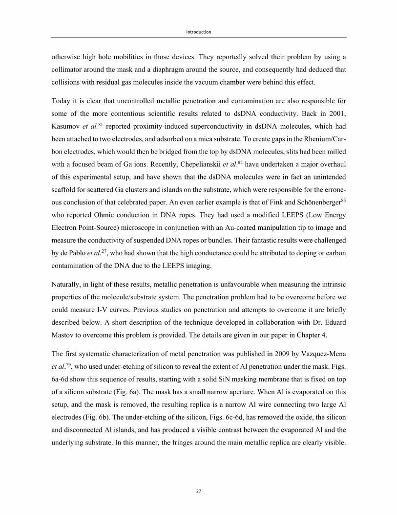
The first systematic characterization of metal penetration was published in 2009 by Vazquez-Mena
et al.79, who used under-etching of silicon to reveal the extent of Al penetration under the mask. Figs.
6a-6d show this sequence of results, starting with a solid SiN masking membrane that is fixed on top
of a silicon substrate (Fig. 6a). The mask has a small narrow aperture. When Al is evaporated on this
setup, and the mask is removed, the resulting replica is a narrow Al wire connecting two large Al
electrodes (Fig. 6b). The under-etching of the silicon, Figs. 6c-6d, has removed the oxide, the silicon
and disconnected Al islands, and has produced a visible contrast between the evaporated Al and the
underlying substrate. In this manner, the fringes around the main metallic replica are clearly visible.
Introduction
28
It should be noted that these fringes were not removed with the silicon, an indication that they are
bound to the main replica.
Figure 6 | Penetration zones and blurring phenomenology. a, SEM image of a stencil aperture and b its corresponding deposited Al structure on a silicon substrate showing the clear correspondence between them. In b, the halo surrounding the deposited structure is hardly visible. c, Scheme of the silicon ‘contrast etching’ used to enhance the contrast of the halo. d, SEM image of the same structure in b, after etching, revealing clearly the halo around the central structure. e, Diagram showing the role of geometry and material spreading in the blurring in stencil lithography (not to scale). The struc-ture consists of a central structure (WC) surrounded by a halo of material due to material spreading. This diagram shows the different elements affecting the blurring: source–substrate distance (D), ma-terial source size (S), stencil–substrate gap (G), stencil aperture width (A) and membrane thickness (T). It also shows the width of the central structure (WC), the width of the total structure including the halo (WT), the blurring due to the geometry (BG = WC − A) and the blurring due to the halo (BH = WT − WC). Taken from Vazquez-Mena et al.79 © IOP Publishing. Reproduced with permission. All rights reserved.
Their geometric approach, depicted schematically in Fig. 6e, splits the penetration into zones of bal-
listic and non-ballistic trajectories. Their basic idea was that at high vacuum, the distance between
the heated source and the target was considerably smaller than the mean free path. Based on this, they
distinguished between two types of penetration: geometrical blurring is the direct result of evaporated
material travelling at ballistic trajectories from the perimeter of the source, resulting in a small “shoul-
der” at either side of the main replica, while halo blurring is the collective term given to all the metal
penetration beyond this shoulder, which could not be reconciled with simple ballistic trajectories.
Geometrical blurring is characterised by the width (see Fig. 6e), which is a function of the geo-
metrical dimensions:
2⁄2⁄
.
a b
d
e
c
Introduction
29
The second equality is an approximation for the typical case when the source-substrate distance (D)
and gap (G) are much larger than the thickness of the mask (T), while the size of the source (S) is
greater than the size of the aperture (A), i.e., , ≫ and ≫ .
The cause of the halo blurring is a complicated issue. Vazquez-Mena et al.79 were conflicted as to the
origins of this effect. While they observed no reduction in the penetration with a substantial decrease
in substrate temperature, they still opted to describe the penetration through surface diffusion, even
though they would argue that it too did not really account for the tens to hundreds of nanometres of
penetration observed79. Moreover, as they claim at the end of that work, theoretical models based
solely on surface diffusion could not account for the extent of the blurring or the pattern of the fringes.
These results seemed to imply that only by closing the gap would it be possible to overcome the
blurring. This is routinely achieved in standard resist-based patterning techniques, which utilise a
chemical polymer as a mask that adheres to the substrate, follows its curvature, and leaves no gap,
with very sharp and well-defined metallic replicas after lift-off. Therefore, the general idea seemed
to centre on mimicking the polymer, but with a solid-state mask instead.
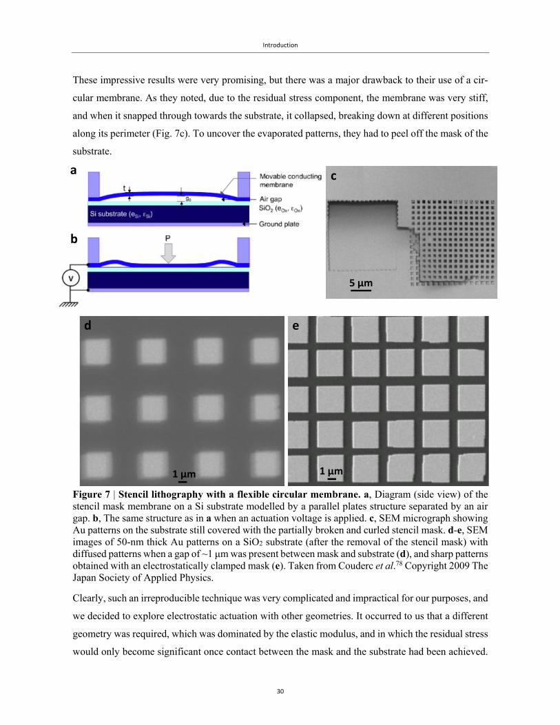
In that same year, Couderc et al.78, who also realized the penetration problem, and the distortion it
could cause, published an important work, in which they tried to fix the situation. They constructed
a thin silicon membrane, which was then highly doped to the point of being nearly metallic (Fig. 7).
They employed this membrane as the mask in a capacitor-like setup, by applying a potential differ-
ence between the membrane and the underlying silicon substrate (Fig. 7a). Due to its flexibility, the
membrane responded to the field, bending with the increasing voltage, until it had reached the unsta-
ble zone of the pull-in instability, and collapsed to the substrate (Fig. 7b-7c). This process is known
as electrostatic clamping84,85.
In this way, they had overcome the restoring mechanical forces in the membrane, and had minimized
the gap substantially. They proceeded to compare the result of gold evaporation on hydroxylated
silicon through patterns in the membrane with and without clamping, and were able to prove une-
quivocally that clamping had worked well to reduce the penetration (Figs. 7d-7e).
Introduction
30
These impressive results were very promising, but there was a major drawback to their use of a cir-
cular membrane. As they noted, due to the residual stress component, the membrane was very stiff,
and when it snapped through towards the substrate, it collapsed, breaking down at different positions
along its perimeter (Fig. 7c). To uncover the evaporated patterns, they had to peel off the mask of the
substrate.
Figure 7 | Stencil lithography with a flexible circular membrane. a, Diagram (side view) of the stencil mask membrane on a Si substrate modelled by a parallel plates structure separated by an air gap. b, The same structure as in a when an actuation voltage is applied. c, SEM micrograph showing Au patterns on the substrate still covered with the partially broken and curled stencil mask. d-e, SEM images of 50-nm thick Au patterns on a SiO2 substrate (after the removal of the stencil mask) with diffused patterns when a gap of ~1 μm was present between mask and substrate (d), and sharp patterns obtained with an electrostatically clamped mask (e). Taken from Couderc et al.78 Copyright 2009 The Japan Society of Applied Physics.
Clearly, such an irreproducible technique was very complicated and impractical for our purposes, and
we decided to explore electrostatic actuation with other geometries. It occurred to us that a different
geometry was required, which was dominated by the elastic modulus, and in which the residual stress
would only become significant once contact between the mask and the substrate had been achieved.
a
b
c
5 μm
d e
1 μm 1 μm
Introduction
31
For this purpose, we experimented with different flexible cantilever membranes, and finally settled
on a commercial cantilever array from Concentris©. The clamping process, and the results, as well as
the physics of the collapse are presented and discussed extensively in Chapter 4. It is important to
note that the main novelty offered by our technique is the reversibility of the clamping, allowing us
to use the same mask in multiple clamping and de-clamping cycles of evaporation, and through elec-
trostatic actuation we have obtained full compliance between the substrate and the mask.
1.4 Researchobjectivesandspecificaims
The main research objective was to investigate the electrical properties of G4-DNA and methodically
determine whether it was capable of supporting electric charge transport while adsorbed on a mica
substrate.
Specfic Aims:
Measure electrostatic polarizability of G4-DNA as a function of the orientation of the strands.
Develop a reliable and reproducible methodology for conductivity measurements of G4-DNA
molecules in a cAFM setup.
Determine the charge transport mechanism through G4-DNA.
1.5 References
1 Watson, J. D. & Crick, F. H. A structure for deoxyribose nucleic acid. Nature 171, 737 (1953). 2 Mullis, K. et al. Specific Enzymatic Amplification of DNA Invitro ‐ the Polymerase Chain‐Reaction. Cold Spring
Harb Sym 51, 263‐273 (1986). 3 Binnig, G., Rohrer, H., Gerber, C. & Weibel, E. Tunneling through a Controllable Vacuum Gap. Appl Phys Lett
40, 178‐180 (1982). 4 Binnig, G., Quate, C. F. & Gerber, C. Atomic Force Microscope. Phys Rev Lett 56, 930‐933 (1986). 5 Seeman, N. C. DNA in a material world. Nature 421, 427‐431 (2003). 6 Seeman, N. C. An overview of structural DNA Nanotechnology. Mol Biotechnol 37, 246‐257 (2007). 7 Rothemund, P. W. K. Folding DNA to create nanoscale shapes and patterns. Nature 440, 297‐302 (2006). 8 Aldaye, F. A., Palmer, A. L. & Sleiman, H. F. Assembling materials with DNA as the guide. Science 321, 1795‐
1799 (2008). 9 Douglas, S. M. et al. Self‐assembly of DNA into nanoscale three‐dimensional shapes. Nature 459, 414‐418
(2009). 10 Pinheiro, A. V., Han, D. R., Shih, W. M. & Yan, H. Challenges and opportunities for structural DNA nanotech‐
nology. Nat Nanotechnol 6, 763‐772 (2011). 11 Eley, D. D. & Spivey, D. I. Semiconductivity of organic substances. Part 9.—Nucleic acid in the dry state. T Far‐
aday Soc 58, 411‐415 (1962). 12 Aviram, A. & Ratner, M. A. Molecular Rectifiers. Chem Phys Lett 29, 277‐283 (1974). 13 Wagenknecht, H. A. Charge Transfer in DNA: From Mechanism to Application. (Wiley‐VCH 2005). 14 Boon, E. M. & Barton, J. K. Charge transport in DNA. Curr Opin Struc Biol 12, 320‐329 (2002). 15 Tal‐Or, L. Novel C‐AFM techniques for measuring dsDNA charge transport properties MSc thesis, Hebrew Uni‐
versity, (2009). 16 Astakhova, T. Y., Likhachev, V. N. & Vinogradov, G. A. Long‐range charge transfer in biopolymers. Russ Chem
Rev+ 81, 994‐1010 (2012).
Introduction
32
17 Muren, N. B., Olmon, E. D. & Barton, J. K. Solution, surface, and single molecule platforms for the study of DNA‐mediated charge transport. Phys Chem Phys 14, 13754‐13771 (2012).
18 Endres, R. G., Cox, D. L. & Singh, R. R. P. Colloquium: The quest for high‐conductance DNA. Rev Mod Phys 76, 195‐214 (2004).
19 Porath, D., Cuniberti, G. & Di Felice, R. Charge transport in DNA‐based devices. Top Curr Chem 237, 183‐227 (2004).
20 Porath, D., Lapidot, N. & Gomez‐Herrero, J. in Introducing Molecular Electronics (eds G. Cuniberti, G. Fagas, & K. Richter) (Springer, 2005).
21 Cuniberti, G., Richter, K. & Fagas, G. in Lecture Notes in Physics Vol. 680 (Springer Berlin Heidelberg, 2005). 22 Cuevas, J. C. & Scheer, E. Molecular Electronics: An Introduction to Theory and Experiment (World Scientific
2010). 23 Lindsay, S. Molecular wires and devices: Advances and issues. Faraday Discuss 131, 403‐409 (2006). 24 Kasumov, A. Y., Klinov, D. V., Roche, P. E., Gueron, S. & Bouchiat, H. Thickness and low‐temperature conduc‐
tivity of DNA molecules. Appl Phys Lett 84, 1007‐1009 (2004). 25 Jortner, J., Bixon, M., Langenbacher, T. & Michel‐Beyerle, M. E. Charge transfer and transport in DNA. P Natl
Acad Sci USA 95, 12759‐12765 (1998). 26 Braun, E., Eichen, Y., Sivan, U. & Ben‐Yoseph, G. DNA‐templated assembly and electrode attachment of a con‐
ducting silver wire. Nature 391, 775‐778 (1998). 27 de Pablo, P. J. et al. Absence of dc‐conductivity in lambda‐DNA. Phys Rev Lett 85, 4992‐4995 (2000). 28 Storm, A. J., van Noort, J., de Vries, S. & Dekker, C. Insulating behavior for DNA molecules between nanoelec‐
trodes at the 100 nm length scale. Appl Phys Lett 79, 3881‐3883 (2001). 29 Briman, M., Armitage, N. P., Helgren, E. & Gruner, G. Dipole relaxation losses in DNA. Nano Lett 4, 733‐736
(2004). 30 Armitage, N. P., Briman, M. & Gruner, G. Charge transfer and charge transport on the double helix. Physica
Status Solidi B‐Basic Research 241, 69‐75 (2004). 31 Kleine, H. et al. Absence of intrinsic electric conductivity in single dsDNA molecules. J Biotechnol 112, 91‐95
(2004). 32 Heim, T., Melin, T., Deresmes, D. & Vuillaume, D. Localization and delocalization of charges injected in DNA.
Appl Phys Lett 85, 2637‐2639 (2004). 33 Heim, T., Deresmes, D. & Vuillaume, D. Conductivity of DNA probed by conducting‐atomic force microscopy:
Effects of contact electrode, DNA structure, and surface interactions. J Appl Phys 96, 2927‐2936 (2004). 34 Zhou, Y. X., Johnson, A. T., Hone, J. & Smith, W. F. Simple fabrication of molecular circuits by shadow mask
evaporation. Nano Lett 3, 1371‐1374 (2003). 35 Gomez‐Navarro, C. et al. Contactless experiments on individual DNA molecules show no evidence for molecu‐
lar wire behavior. P Natl Acad Sci USA 99, 8484‐8487 (2002). 36 Porath, D., Bezryadin, A., de Vries, S. & Dekker, C. Direct measurement of electrical transport through DNA
molecules. Nature 403, 635‐638 (2000). 37 Roy, S. et al. Direct electrical measurements on single‐molecule genomic DNA using single‐walled carbon
nanotubes. Nano Lett 8, 26‐30 (2008). 38 Guo, X. F., Gorodetsky, A. A., Hone, J., Barton, J. K. & Nuckolls, C. Conductivity of a single DNA duplex bridging
a carbon nanotube gap. Nat Nanotechnol 3, 163‐167 (2008). 39 Cohen, H., Nogues, C., Naaman, R. & Porath, D. Direct measurement of electrical transport through single
DNA molecules of complex sequence. P Natl Acad Sci USA 102, 11589‐11593 (2005). 40 Liu, S. P. et al. Electronic transport through short dsDNA measured with mechanically controlled break junc‐
tions: New thiol‐gold binding protocol improves conductance. Phys Status Solidi B 250, 2342‐2348 (2013). 41 Bardavid, Y., Ghabboun, J., Porath, D., Kotylar, A. B. & Yitzchaik, S. Formation of polyaniline layer on DNA by
electrochemical polymerization. Polymer 49, 2217‐2222 (2008). 42 Ma, Y. F., Zhang, J. M., Zhang, G. J. & He, H. X. Polyaniline nanowires on Si surfaces fabricated with DNA tem‐
plates. J Am Chem Soc 126, 7097‐7101 (2004). 43 Kumar, A., Hwang, J. H., Kumar, S. & Nam, J. M. Tuning and assembling metal nanostructures with DNA. Chem
Commun 49, 2597‐2609 (2013). 44 Rakitin, A. et al. Metallic conduction through engineered DNA: DNA nanoelectronic building blocks. Phys Rev
Lett 86, 3670‐3673 (2001). 45 Kotlyar, A. B. et al. Long, monomolecular guanine‐based nanowires. Adv Mater 17, 1901‐1904 (2005). 46 Cohen, H. et al. Polarizability of G4‐DNA observed by electrostatic force microscopy measurements. Nano
Lett 7, 981‐986 (2007).
Introduction
33
47 Borovok, N. et al. Assembling of G‐strands into novel tetra‐molecular parallel G4‐DNA nanostructures using avidinbiotin recognition. Nucleic Acids Res 36, 5050‐5060 (2008).
48 Livshits, G. I., Ghabboun, J., Borovok, N., Kotlyar, A. & Porath, D. Comparative EFM of mono‐ and tetra‐molec‐ular G4‐DNA. Adv Mater 26, 4981‐4985 (2014).
49 Fritzsche, W. & Spindler, L. Guanine Quartets : Structure and Application. (RSC Publishing, 2013). 50 Davis, J. T. G‐quartets 40 years later: From 5 '‐GMP to molecular biology and supramolecular chemistry. An‐
gew Chem Int Edit 43, 668‐698 (2004). 51 Maizels, N. Dynamic roles for G4 DNA in the biology of eukaryotic cells. Nat Struct Mol Biol 13, 1055‐1059
(2006). 52 Cai, L. T., Tabata, H. & Kawai, T. Self‐assembled DNA networks and their electrical conductivity. Appl Phys Lett
77, 3105‐3106 (2000). 53 Shapir, E. et al. High‐resolution STM imaging of novel single G4‐DNA molecules. J Phys Chem B 112, 9267‐
9269 (2008). 54 Roger‐Eitan, I. et al. High‐Resolution Scanning Tunneling Microscopy Imaging of Biotin‐Avidin‐G4‐DNA Mole‐
cules. J Phys Chem C 117, 22462‐22465 (2013). 55 Kubar, T., Woiczikowski, P. B., Cuniberti, G. & Elstner, M. Efficient calculation of charge‐transfer matrix ele‐
ments for hole transfer in DNA. J Phys Chem B 112, 7937‐7947 (2008). 56 Di Felice, R., Calzolari, A., Garbesi, A., Alexandre, S. S. & Soler, J. M. Strain‐dependence of the electronic prop‐
erties in periodic quadruple helical G4‐wires. J Phys Chem B 109, 22301‐22307 (2005). 57 Marsh, T. C., Vesenka, J. & Henderson, E. A New DNA Nanostructure, the G‐Wire, Imaged by Scanning Probe
Microscopy. Nucleic Acids Res 23, 696‐700 (1995). 58 Protozanova, E. & Macgregor, R. B. Frayed wires: A thermally stable form of DNA with two distinct structural
domains. Biochemistry‐Us 35, 16638‐16645 (1996). 59 Sen, D. & Gilbert, W. Novel DNA Superstructures Formed by Telomere‐Like Oligomers. Biochemistry‐Us 31,
65‐70 (1992). 60 Borovok, N., Molotsky, T., Ghabboun, J., Porath, D. & Kotlyar, A. Efficient procedure of preparation and prop‐
erties of long uniform G4‐DNA nanowires. Anal Biochem 374, 71‐78 (2008). 61 Wilchek, M. & Bayer, E. A. Introduction to Avidin‐Biotin Technology. Method Enzymol 184, 5‐13 (1990). 62 Garcia, R. & Perez, R. Dynamic atomic force microscopy methods. Surf Sci Rep 47, 197‐301 (2002). 63 Woiczikowski, P. B., Kubar, T., Gutierrez, R., Cuniberti, G. & Elstner, M. Structural stability versus conforma‐
tional sampling in biomolecular systems: Why is the charge transfer efficiency in G4‐DNA better than in dou‐ble‐stranded DNA? J Chem Phys 133, 035103 (2010).
64 Liu, S. P. et al. Direct Measurement of Electrical Transport Through G‐Quadruplex DNA with Mechanically Controllable Break Junction Electrodes. Angew Chem Int Edit 49, 3313‐3316 (2010).
65 Parviainen, T., Eidelshtein, G., Kotlyar, A. & Toppari, J. J. in Guanine Quartets: Structure and Application (eds Wolfgang Fritzsche & Lea Spindler) (RSC Publishing, 2013).
66 Marsh, T. C. & Vesenka, J. in Nano and molecular electronics handbook (ed S. E. Lyshevski) (CRC Press, 2007).
67 Lindsay, S. M. Introduction to Nanoscience. (Oxford University Press, 2010). 68 Moth‐Poulsen, K. & Bjornholm, T. Molecular electronics with single molecules in solid‐state devices. Nat Nan‐
otechnol 4, 551‐556 (2009). 69 Deshmukh, M. M., Ralph, D. C., Thomas, M. & Silcox, J. Nanofabrication using a stencil mask. Appl Phys Lett
75, 1631‐1633 (1999). 70 Vazquez‐Mena, O. et al. Metallic Nanowires by Full Wafer Stencil Lithography. Nano Lett 8, 3675‐3682 (2008). 71 Vazquez‐Mena, O., Sannomiya, T., Villanueva, L. G., Voros, J. & Brugger, J. Metallic Nanodot Arrays by Stencil
Lithography for Plasmonic Biosensing Applications. Acs Nano 5, 844‐853 (2011). 72 Welte, L., Calzolari, A., Di Felice, R., Zamora, F. & Gomez‐Herrero, J. Highly conductive self‐assembled nano‐
ribbons of coordination polymers. Nat Nanotechnol 5, 110‐115 (2010). 73 Sidler, K. et al. Resistivity measurements of gold wires fabricated by stencil lithography on flexible polymer
substrates. Microelectronic Engineering 85, 1108‐1111 (2008). 74 Villanueva, L. G. et al. All‐stencil transistor fabrication on 3D silicon substrates. Journal of Micromechanics
and Microengineering 22, 095022 (2012). 75 Vazquez‐Mena, O. et al. High‐Resolution Resistless Nanopatterning on Polymer and Flexible Substrates for
Plasmonic Biosensing Using Stencil Masks. Acs Nano 6, 5474‐5481 (2012). 76 Racz, Z. & Seabaugh, A. Characterization and control of unconfined lateral diffusion under stencil masks. J Vac
Sci Technol B 25, 857‐861 (2007).
Introduction
34
77 Egger, S. et al. Dynamic shadow mask technique: A universal tool for nanoscience. Nano Letters 5, 15‐20 (2005).
78 Couderc, S., Blech, V. & Kim, B. New Surface Treatment and Microscale/Nanoscale Surface Patterning Using Electrostatically Clamped Stencil Mask. Japanese Journal of Applied Physics 48, 095007 (2009).
79 Vazquez‐Mena, O. et al. Analysis of the blurring in stencil lithography. Nanotechnology 20, 415303 (2009). 80 Podzorov, V., Sysoev, S. E., Loginova, E., Pudalov, V. M. & Gershenson, M. E. Single‐crystal organic field effect
transistors with the hole mobility similar to 8 cm(2)/V s. Appl Phys Lett 83, 3504‐3506 (2003). 81 Kasumov, A. Y. et al. Proximity‐induced superconductivity in DNA. Science 291, 280‐282 (2001). 82 Chepelianskii, A. D. et al. Long range electronic transport in DNA molecules deposited across a disconnected
array of metallic nanoparticles. Cr Phys 13, 967‐992 (2012). 83 Fink, H. W. & Schonenberger, C. Electrical conduction through DNA molecules. Nature 398, 407‐410 (1999). 84 Rebeiz, G. M. RF MEMS: Theory, Design and Technology. (John Wiley & Sons, 2003). 85 Senturia, S. D. Microsystem Design. (Kluwer Academic Pulishers, 2002).
35
Comparative electrostatic forcemicroscopy of tetra‐ and intra‐molecular G4‐DNAAdvanced Materials 26(29), pp. 4981 – 4985, August 6, 2014. Copyright Wiley-VCH Verlag GmbH & Co. KGaA. Reproduced with permission.
Comparative EFM G4‐DNA
36
2.1 Mainmanuscript
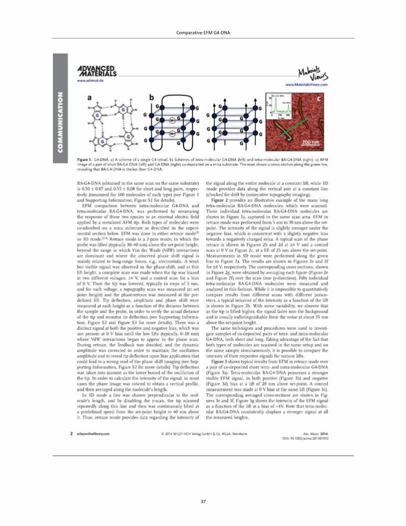
Comparative EFM G4‐DNA
37
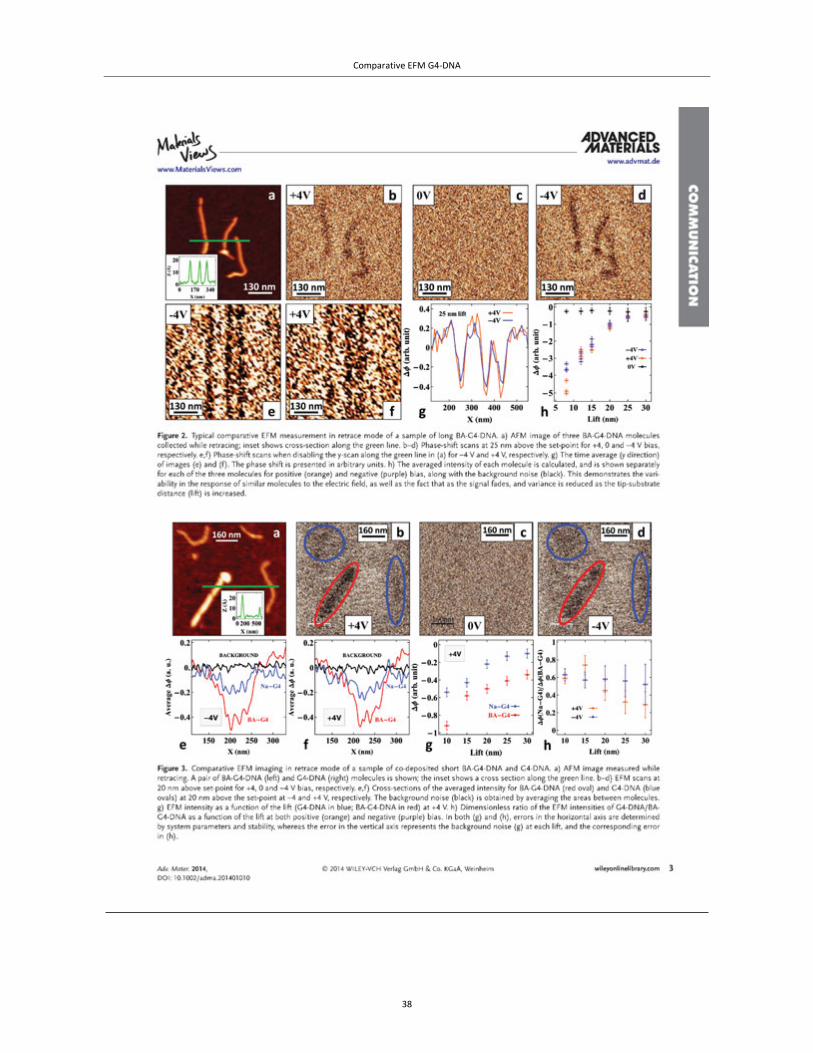
Comparative EFM G4‐DNA
38
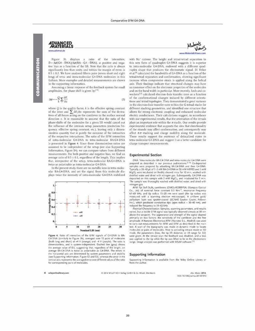
Comparative EFM G4‐DNA
39
Comparative EFM G4‐DNA
40
Comparative EFM G4‐DNA
41
2.2 Supplementaryinformation
Comparative EFM G4‐DNA
42
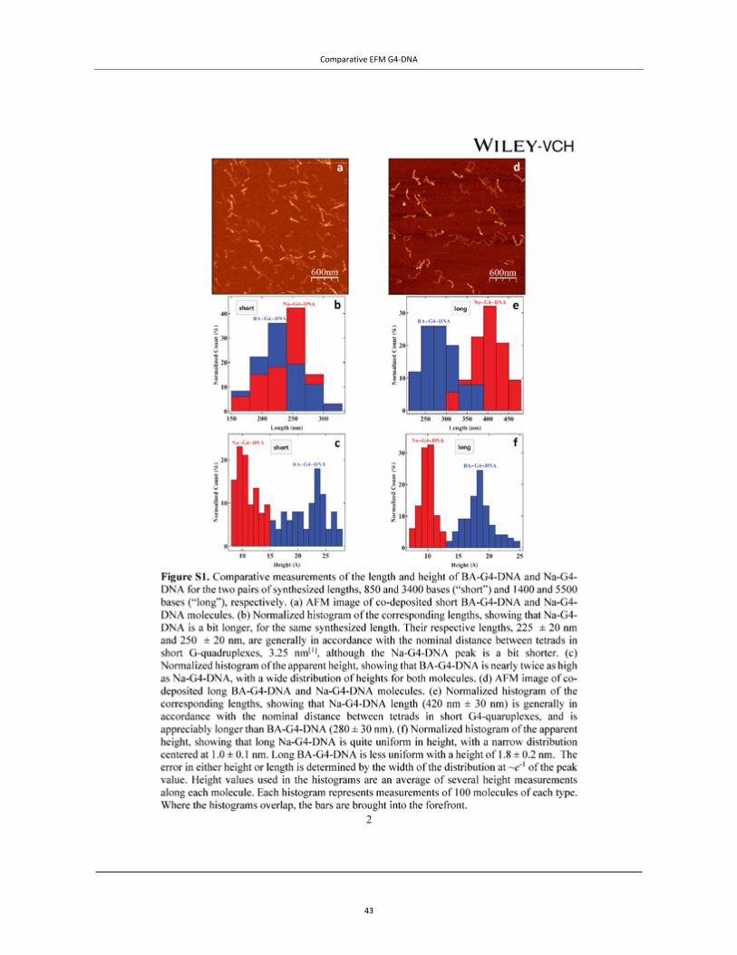
Comparative EFM G4‐DNA
43
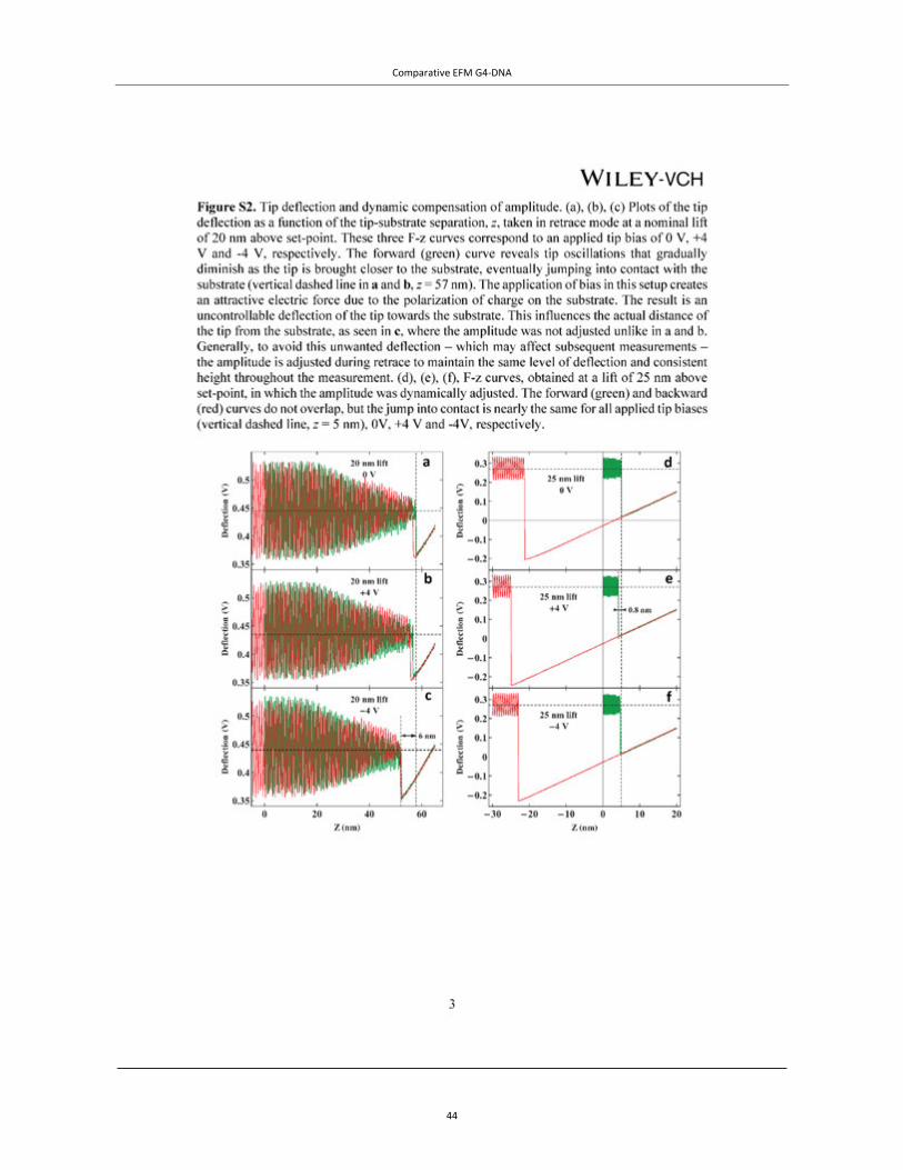
Comparative EFM G4‐DNA
44
Comparative EFM G4‐DNA
45
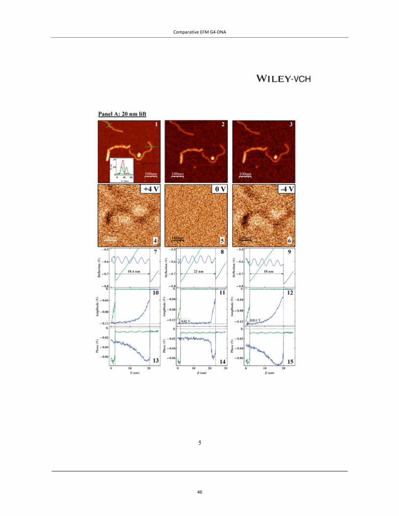
Comparative EFM G4‐DNA
46
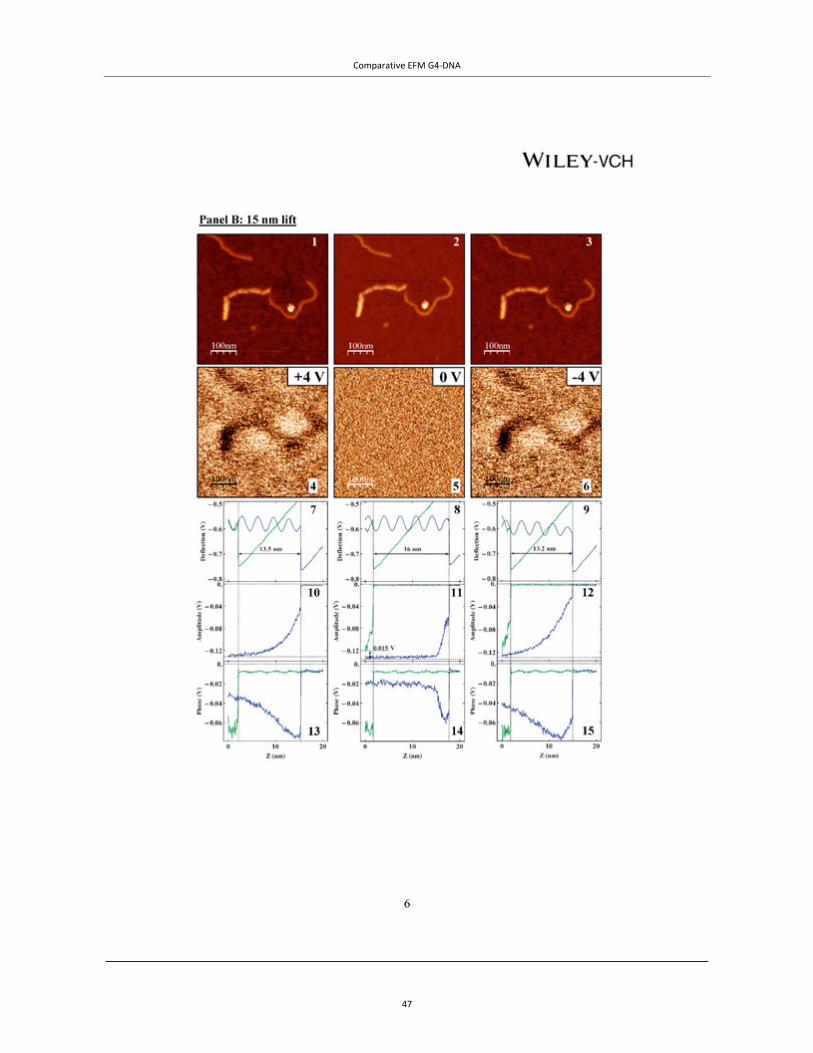
Comparative EFM G4‐DNA
47
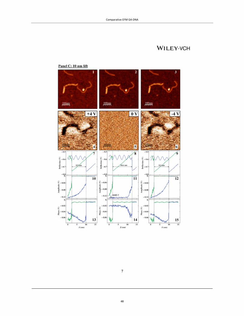
Comparative EFM G4‐DNA
48
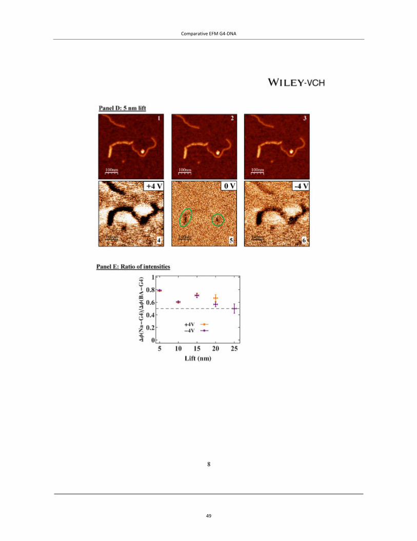
Comparative EFM G4‐DNA
49
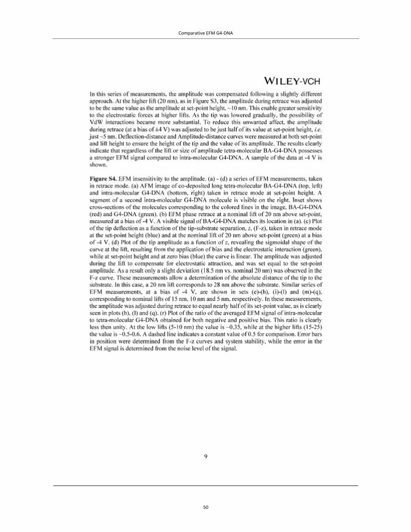
Comparative EFM G4‐DNA
50
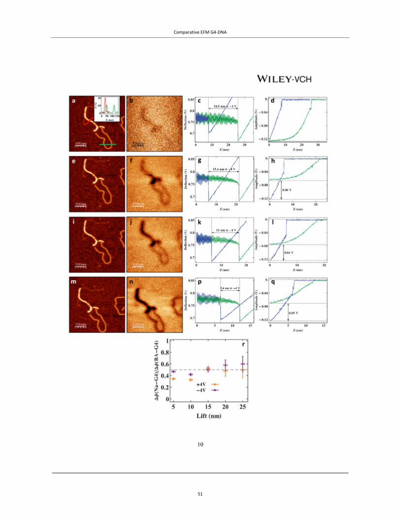
Comparative EFM G4‐DNA
51

Comparative EFM G4‐DNA
52
53
Long‐range charge transport insingleG‐quadruplexDNAmoleculesNature Nanotechnology, In Press (2014).
Charge transport in G4‐DNA
54
3.1 Mainmanuscript
Content removed from online version due to copyright. Article may be found at http://www.nature.com/nnano/jour-nal/v9/n12/full/nnano.2014.246.html

Charge transport in G4‐DNA
55
Content removed from online version due to copyright. Article may be found at http://www.nature.com/nnano/jour-nal/v9/n12/full/nnano.2014.246.html

Charge transport in G4‐DNA
56
Content removed from online version due to copyright. Article may be found at http://www.nature.com/nnano/jour-nal/v9/n12/full/nnano.2014.246.html

Charge transport in G4‐DNA
57
Content removed from online version due to copyright. Article may be found at http://www.nature.com/nnano/jour-nal/v9/n12/full/nnano.2014.246.html

Charge transport in G4‐DNA
58
Content removed from online version due to copyright. Article may be found at http://www.nature.com/nnano/jour-nal/v9/n12/full/nnano.2014.246.html

Charge transport in G4‐DNA
59
Content removed from online version due to copyright. Article may be found at http://www.nature.com/nnano/jour-nal/v9/n12/full/nnano.2014.246.html

Charge transport in G4‐DNA
60
Content removed from online version due to copyright. Article may be found at http://www.nature.com/nnano/jour-nal/v9/n12/full/nnano.2014.246.html
61
3.2 Supplementaryinformation
Supplementary Information for
Long-range transport in single G-quadruplex DNA molecules
Gideon I. Livshits, Avigail Stern, Dvir Rotem, Natalia Borovok, Gennady Eidelshtein, Ago-stino Migliore, Erika Penzo, Shalom J. Wind, Rosa Di Felice, Spiros S. Skourtis, Juan Car-
los Cuevas, Leonid Gurevich, Alexander B. Kotlyar, Danny Porath
Below we provide further samples of experimental data and results of control experiments, as well as more detailed explanations for the theoretical modelling and calculations. Specifically, we first illustrate in section 1 the methodology that we have used to produce a sharp and well-defined electrode border with a clean nearby surface. This procedure enables to forms a well-defined electrical coupling with the molecule that protrudes from the border for the I-V measurements. Then, we show morphological evidence that suggests the formation of strong coupling between the evaporated electrode and the molecules used in these experiments. We add numerous additional examples (cited in the manuscript) from our measured data.
In section 2, the hopping model discussed in the main text is explained in greater detail and the fits of additional sets of I-V measurements are shown. In particular, we have included a table summarizing the fitting parame-ters. Section 3 is devoted to the description of the ab initio calculations of the electronic coupling between neighbouring G-tetrads. Estimates of the intra-molecular rate of G4-DNA based on those calculations are pre-sented in section 4. Additional references are provided in section 5.
1. Experimental part
A central and known problem in evaporation of electrodes is the penetration of evaporated metal under the mask. This problem is usually caused by the distance between the mask and the surface, as shown in Supple-mentary Fig. 1a below (adapted from Vazquez-Mena et al.1). Such a penetration strongly affects measurement on soft polymers, especially those with a length comparable or shorter than the penetration length. The main issue is the coverage of the molecules by metal clusters and atoms on the surface, preventing reliable conduc-tion measurements along the molecule. In our setup, a silicon stencil mask is reversibly electrostatically clamped to the substrate during evaporation, based on the same principles as in Couderc et al.2 illustrated in Supplementary Fig. 1b, thus forming a sharp border with a clean surface beyond the border. Supplementary Figs. 1c and 1e and their respective cross sections in Supplementary Figs. 1d and 1f show the penetration when the mask attachment to the surface is loose. There are molecules under the metal, which can be barely seen. Supplementary Fig. 1g is an example of the evaporation of gold following good attachment of the mask to the surface that prevents penetration and forms a sharp border, as is also illustrated in the cross section in Supple-mentary Fig. 1h. In this case, two protruding molecules can be seen. Scanning electron microscope imaging shows that the border in our samples is even sharper than is observed in the AFM images, where the resolution is limited by tip dilation. The scanning electron microscope image in the inset of Supplementary Fig. 1g shows that the area beyond the border is clean of metal clusters.
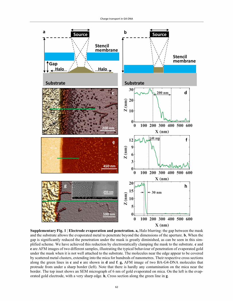
Charge transport in G4‐DNA
62
Supplementary Fig. 1 | Electrode evaporation and penetration. a, Halo blurring: the gap between the mask and the substrate allows the evaporated metal to penetrate beyond the dimensions of the aperture. b, When the gap is significantly reduced the penetration under the mask is greatly diminished, as can be seen in this sim-plified scheme. We have achieved this reduction by electrostatically clamping the mask to the substrate. c and e are AFM images of two different samples, illustrating the typical behaviour of penetration of evaporated gold under the mask when it is not well attached to the substrate. The molecules near the edge appear to be covered by scattered metal clusters, extending into the mica for hundreds of nanometres. Their respective cross sections along the green lines in c and e are shown in d and f. g, AFM image of two BA-G4-DNA molecules that protrude from under a sharp border (left). Note that there is hardly any contamination on the mica near the border. The top inset shows an SEM micrograph of 6 nm of gold evaporated on mica. On the left is the evap-orated gold electrode, with a very sharp edge. h, Cross section along the green line in g.
h
f
c
200 nm
e
450 nm
d
b
Stencil membrane
Source
Substrate
a
Stencil membrane
Source
Gap Halo Halo
Substrate
g
100 nm
250 nm
0 100 200 300 400 500 6000
10
20
30
X nm
Znm
200 nm
0 100 200 300 400 500 6000
5
10
15
20
X nm
Znm 30 nm
0 100 200 300 400 500 6000
3
6
9
12
X nm
Znm
140 nm
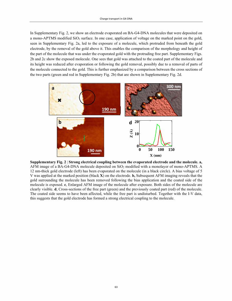
Charge transport in G4‐DNA
63
In Supplementary Fig. 2, we show an electrode evaporated on BA-G4-DNA molecules that were deposited on a mono-APTMS modified SiO2 surface. In one case, application of voltage on the marked point on the gold, seen in Supplementary Fig. 2a, led to the exposure of a molecule, which protruded from beneath the gold electrode, by the removal of the gold above it. This enables the comparison of the morphology and height of the part of the molecule that was under the evaporated gold with the protruding free part. Supplementary Figs. 2b and 2c show the exposed molecule. One sees that gold was attached to the coated part of the molecule and its height was reduced after evaporation or following the gold removal, possibly due to a removal of parts of the molecule connected to the gold. This is further emphasized by a comparison between the cross sections of the two parts (green and red in Supplementary Fig. 2b) that are shown in Supplementary Fig. 2d.
Supplementary Fig. 2 | Strong electrical coupling between the evaporated electrode and the molecule. a, AFM image of a BA-G4-DNA molecule deposited on SiO2 modified with a monolayer of mono-APTMS. A 12 nm-thick gold electrode (left) has been evaporated on the molecule (in a black circle). A bias voltage of 5 V was applied at the marked position (black X) on the electrode. b, Subsequent AFM imaging reveals that the gold surrounding the molecule has been removed following the bias application and the coated side of the molecule is exposed. c, Enlarged AFM image of the molecule after exposure. Both sides of the molecule are clearly visible. d, Cross-sections of the free part (green) and the previously coated part (red) of the molecule. The coated side seems to have been affected, while the free part is undisturbed. Together with the I-V data, this suggests that the gold electrode has formed a strong electrical coupling to the molecule.
0 50 100 1500
10
20
X nm
Z
d
190 nm
a
190 nm
b
c 300 nm
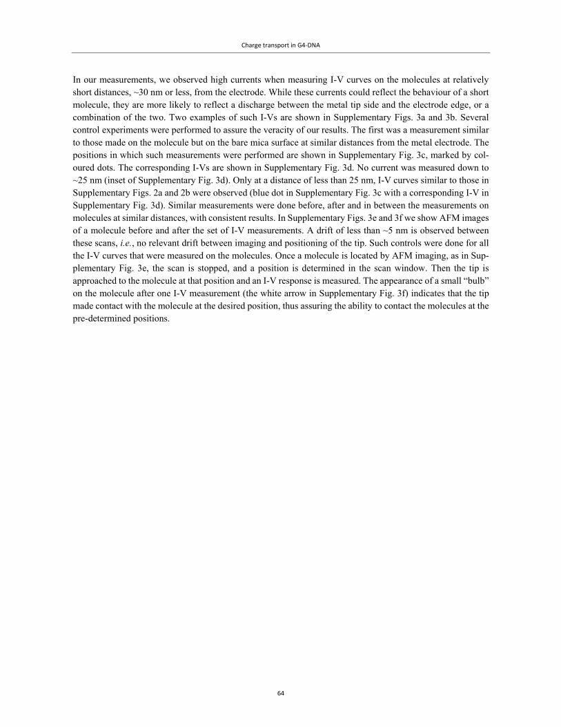
Charge transport in G4‐DNA
64
In our measurements, we observed high currents when measuring I-V curves on the molecules at relatively short distances, ~30 nm or less, from the electrode. While these currents could reflect the behaviour of a short molecule, they are more likely to reflect a discharge between the metal tip side and the electrode edge, or a combination of the two. Two examples of such I-Vs are shown in Supplementary Figs. 3a and 3b. Several control experiments were performed to assure the veracity of our results. The first was a measurement similar to those made on the molecule but on the bare mica surface at similar distances from the metal electrode. The positions in which such measurements were performed are shown in Supplementary Fig. 3c, marked by col-oured dots. The corresponding I-Vs are shown in Supplementary Fig. 3d. No current was measured down to ~25 nm (inset of Supplementary Fig. 3d). Only at a distance of less than 25 nm, I-V curves similar to those in Supplementary Figs. 2a and 2b were observed (blue dot in Supplementary Fig. 3c with a corresponding I-V in Supplementary Fig. 3d). Similar measurements were done before, after and in between the measurements on molecules at similar distances, with consistent results. In Supplementary Figs. 3e and 3f we show AFM images of a molecule before and after the set of I-V measurements. A drift of less than ~5 nm is observed between these scans, i.e., no relevant drift between imaging and positioning of the tip. Such controls were done for all the I-V curves that were measured on the molecules. Once a molecule is located by AFM imaging, as in Sup-plementary Fig. 3e, the scan is stopped, and a position is determined in the scan window. Then the tip is approached to the molecule at that position and an I-V response is measured. The appearance of a small “bulb” on the molecule after one I-V measurement (the white arrow in Supplementary Fig. 3f) indicates that the tip made contact with the molecule at the desired position, thus assuring the ability to contact the molecules at the pre-determined positions.
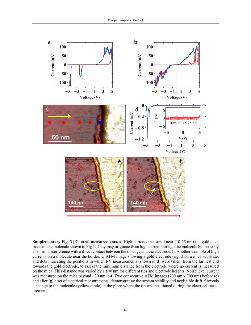
Charge transport in G4‐DNA
65
Supplementary Fig. 3 | Control measurements. a, High currents measured near (10-25 nm) the gold elec-trode on the molecule shown in Fig 1. They may originate from high current through the molecule but possibly also from interference with a direct contact between the tip edge and the electrode. b, Another example of high currents on a molecule near the border. c, AFM image showing a gold electrode (right) on a mica substrate, and dots indicating the positions in which I-V measurements (shown in d) were taken, from the farthest end towards the gold electrode, to assess the minimum distance from the electrode where no current is measured on the mica. This distance was varied by a few nm for different tips and electrode heights. Noise level current was measured on the mica beyond ~30 nm. e-f, Two consecutive AFM images (700 nm x 700 nm) before (e) and after (g) a set of electrical measurements, demonstrating the system stability and negligible drift. f reveals a change to the molecule (yellow circle) in the place where the tip was positioned during the electrical meas-urement.
b a
c d
60 nm
140 nm
e f
140 nm
5 3 1 1 3 5
100
50
0
50
100
Voltage V
CurrentnA
5 3 1 1 3 5
100
50
0
50
100
Voltage V
CurrentnA
531135
0
0.4
0.8
1.2
Voltage V
CurrentnA
505
6
0
6
V V
IpA
125,90,45,25 nm
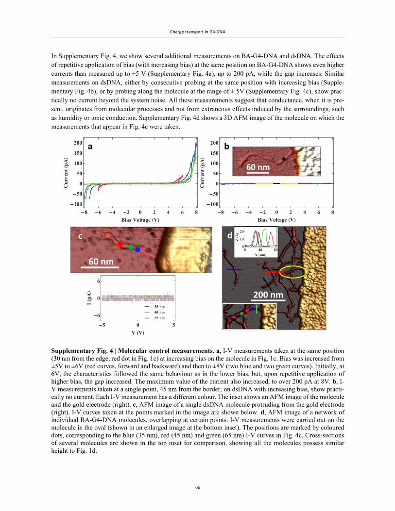
Charge transport in G4‐DNA
66
In Supplementary Fig. 4, we show several additional measurements on BA-G4-DNA and dsDNA. The effects of repetitive application of bias (with increasing bias) at the same position on BA-G4-DNA shows even higher currents than measured up to ±5 V (Supplementary Fig. 4a), up to 200 pA, while the gap increases. Similar measurements on dsDNA, either by consecutive probing at the same position with increasing bias (Supple-mentary Fig. 4b), or by probing along the molecule at the range of ± 5V (Supplementary Fig. 4c), show prac-tically no current beyond the system noise. All these measurements suggest that conductance, when it is pre-sent, originates from molecular processes and not from extraneous effects induced by the surroundings, such as humidity or ionic conduction. Supplementary Fig. 4d shows a 3D AFM image of the molecule on which the measurements that appear in Fig. 4c were taken.
Supplementary Fig. 4 | Molecular control measurements. a, I-V measurements taken at the same position (30 nm from the edge, red dot in Fig. 1c) at increasing bias on the molecule in Fig. 1c. Bias was increased from ±5V to ±6V (red curves, forward and backward) and then to ±8V (two blue and two green curves). Initially, at 6V, the characteristics followed the same behaviour as in the lower bias, but, upon repetitive application of higher bias, the gap increased. The maximum value of the current also increased, to over 200 pA at 8V. b, I-V measurements taken at a single point, 45 nm from the border, on dsDNA with increasing bias, show practi-cally no current. Each I-V measurement has a different colour. The inset shows an AFM image of the molecule and the gold electrode (right). c, AFM image of a single dsDNA molecule protruding from the gold electrode (right). I-V curves taken at the points marked in the image are shown below. d, AFM image of a network of individual BA-G4-DNA molecules, overlapping at certain points. I-V measurements were carried out on the molecule in the oval (shown in an enlarged image at the bottom inset). The positions are marked by coloured dots, corresponding to the blue (35 nm), red (45 nm) and green (65 nm) I-V curves in Fig. 4c. Cross-sections of several molecules are shown in the top inset for comparison, showing all the molecules possess similar height to Fig. 1d.
b a
c d
60 nm
200 nm
60 nm
0 40 800
10
20
X nm
Z
505
6
0
6
V V
IpA
55 nm
40 nm
35 nm
8 6 4 2 0 2 4 6 8
100
50
0
50
100
150
200
Bias Voltage V
CurrentpA
8 6 4 2 0 2 4 6 8
100
50
0
50
100
150
200
Bias Voltage V
CurrentpA
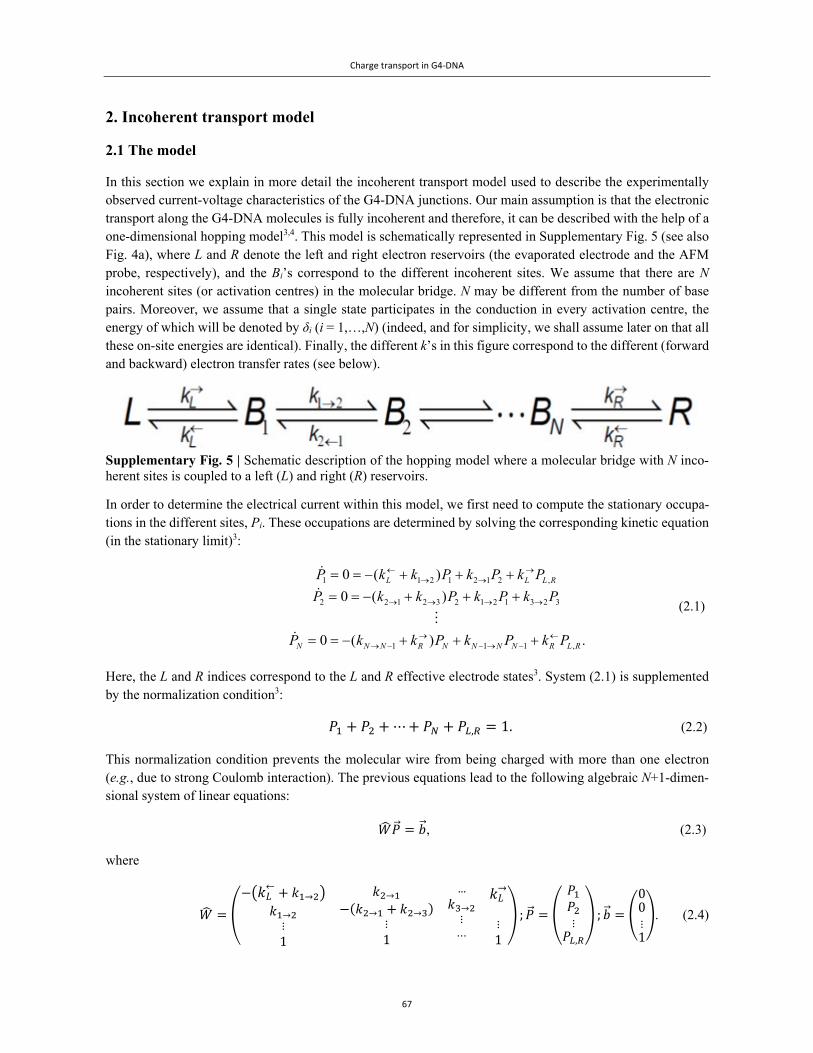
Charge transport in G4‐DNA
67
2. Incoherent transport model
2.1 The model
In this section we explain in more detail the incoherent transport model used to describe the experimentally observed current-voltage characteristics of the G4-DNA junctions. Our main assumption is that the electronic transport along the G4-DNA molecules is fully incoherent and therefore, it can be described with the help of a one-dimensional hopping model3,4. This model is schematically represented in Supplementary Fig. 5 (see also Fig. 4a), where L and R denote the left and right electron reservoirs (the evaporated electrode and the AFM probe, respectively), and the Bi’s correspond to the different incoherent sites. We assume that there are N incoherent sites (or activation centres) in the molecular bridge. N may be different from the number of base pairs. Moreover, we assume that a single state participates in the conduction in every activation centre, the energy of which will be denoted by δi (i = 1,…,N) (indeed, and for simplicity, we shall assume later on that all these on-site energies are identical). Finally, the different k’s in this figure correspond to the different (forward and backward) electron transfer rates (see below).
Supplementary Fig. 5 | Schematic description of the hopping model where a molecular bridge with N inco-herent sites is coupled to a left (L) and right (R) reservoirs.
In order to determine the electrical current within this model, we first need to compute the stationary occupa-tions in the different sites, Pi. These occupations are determined by solving the corresponding kinetic equation (in the stationary limit)3:
1 1 2 1 2 1 2 ,
2 2 1 2 3 2 1 2 1 3 2 3
1 1 1 ,
0 ( )
0 ( )
0 ( ) .
L L L R
N N N R N N N N R L R
P k k P k P k P
P k k P k P k P
P k k P k P k P
(2.1)
Here, the L and R indices correspond to the L and R effective electrode states3. System (2.1) is supplemented by the normalization condition3:
⋯ , 1. (2.2)
This normalization condition prevents the molecular wire from being charged with more than one electron (e.g., due to strong Coulomb interaction). The previous equations lead to the following algebraic N+1-dimen-sional system of linear equations:
, (2.3)
where
←→
→⋮1
→
→ →⋮1
…
→⋮⋯
→
⋮1
;⋮,
;
00⋮1
. (2.4)
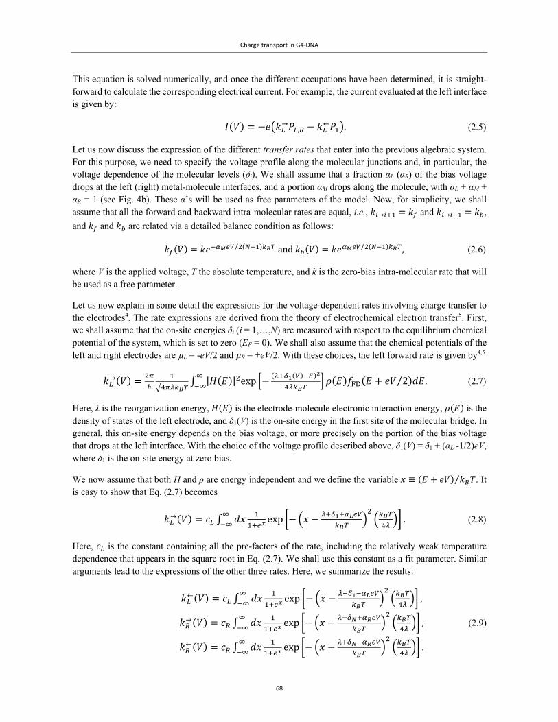
Charge transport in G4‐DNA
68
This equation is solved numerically, and once the different occupations have been determined, it is straight-forward to calculate the corresponding electrical current. For example, the current evaluated at the left interface is given by:
→,
← . (2.5)
Let us now discuss the expression of the different transfer rates that enter into the previous algebraic system. For this purpose, we need to specify the voltage profile along the molecular junctions and, in particular, the voltage dependence of the molecular levels (δi). We shall assume that a fraction αL (αR) of the bias voltage drops at the left (right) metal-molecule interfaces, and a portion αM drops along the molecule, with αL + αM + αR = 1 (see Fig. 4b). These α’s will be used as free parameters of the model. Now, for simplicity, we shall assume that all the forward and backward intra-molecular rates are equal, i.e., → and → ,
and and are related via a detailed balance condition as follows:
⁄ and ⁄ , (2.6)
where V is the applied voltage, T the absolute temperature, and k is the zero-bias intra-molecular rate that will be used as a free parameter.
Let us now explain in some detail the expressions for the voltage-dependent rates involving charge transfer to the electrodes4. The rate expressions are derived from the theory of electrochemical electron transfer5. First, we shall assume that the on-site energies δi (i = 1,…,N) are measured with respect to the equilibrium chemical potential of the system, which is set to zero (EF = 0). We shall also assume that the chemical potentials of the left and right electrodes are µL = -eV/2 and µR = +eV/2. With these choices, the left forward rate is given by4,5
→ | | exp 2⁄ . (2.7)
Here, λ is the reorganization energy, is the electrode-molecule electronic interaction energy, is the density of states of the left electrode, and δ1(V) is the on-site energy in the first site of the molecular bridge. In general, this on-site energy depends on the bias voltage, or more precisely on the portion of the bias voltage that drops at the left interface. With the choice of the voltage profile described above, δ1(V) = δ1 + (αL -1/2)eV, where δ1 is the on-site energy at zero bias.
We now assume that both H and ρ are energy independent and we define the variable ≡ ⁄ . It is easy to show that Eq. (2.7) becomes
→ exp . (2.8)
Here, is the constant containing all the pre-factors of the rate, including the relatively weak temperature dependence that appears in the square root in Eq. (2.7). We shall use this constant as a fit parameter. Similar arguments lead to the expressions of the other three rates. Here, we summarize the results:
← exp ,
→ exp ,
← exp .
(2.9)
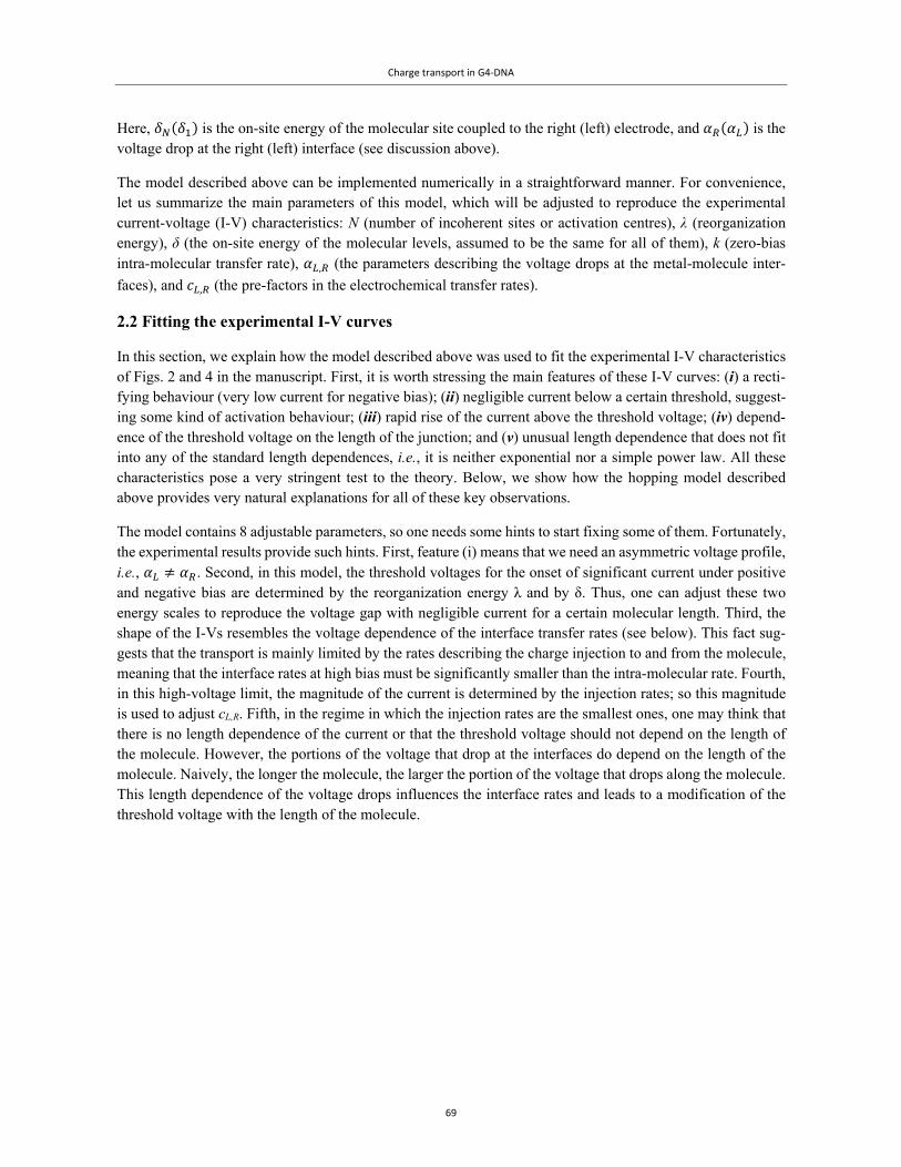
Charge transport in G4‐DNA
69
Here, is the on-site energy of the molecular site coupled to the right (left) electrode, and is the voltage drop at the right (left) interface (see discussion above).
The model described above can be implemented numerically in a straightforward manner. For convenience, let us summarize the main parameters of this model, which will be adjusted to reproduce the experimental current-voltage (I-V) characteristics: N (number of incoherent sites or activation centres), λ (reorganization energy), δ (the on-site energy of the molecular levels, assumed to be the same for all of them), k (zero-bias intra-molecular transfer rate), , (the parameters describing the voltage drops at the metal-molecule inter-
faces), and , (the pre-factors in the electrochemical transfer rates).
2.2 Fitting the experimental I-V curves
In this section, we explain how the model described above was used to fit the experimental I-V characteristics of Figs. 2 and 4 in the manuscript. First, it is worth stressing the main features of these I-V curves: (i) a recti-fying behaviour (very low current for negative bias); (ii) negligible current below a certain threshold, suggest-ing some kind of activation behaviour; (iii) rapid rise of the current above the threshold voltage; (iv) depend-ence of the threshold voltage on the length of the junction; and (v) unusual length dependence that does not fit into any of the standard length dependences, i.e., it is neither exponential nor a simple power law. All these characteristics pose a very stringent test to the theory. Below, we show how the hopping model described above provides very natural explanations for all of these key observations.
The model contains 8 adjustable parameters, so one needs some hints to start fixing some of them. Fortunately, the experimental results provide such hints. First, feature (i) means that we need an asymmetric voltage profile, i.e., . Second, in this model, the threshold voltages for the onset of significant current under positive and negative bias are determined by the reorganization energy λ and by δ. Thus, one can adjust these two energy scales to reproduce the voltage gap with negligible current for a certain molecular length. Third, the shape of the I-Vs resembles the voltage dependence of the interface transfer rates (see below). This fact sug-gests that the transport is mainly limited by the rates describing the charge injection to and from the molecule, meaning that the interface rates at high bias must be significantly smaller than the intra-molecular rate. Fourth, in this high-voltage limit, the magnitude of the current is determined by the injection rates; so this magnitude is used to adjust cL,R. Fifth, in the regime in which the injection rates are the smallest ones, one may think that there is no length dependence of the current or that the threshold voltage should not depend on the length of the molecule. However, the portions of the voltage that drop at the interfaces do depend on the length of the molecule. Naively, the longer the molecule, the larger the portion of the voltage that drops along the molecule. This length dependence of the voltage drops influences the interface rates and leads to a modification of the threshold voltage with the length of the molecule.
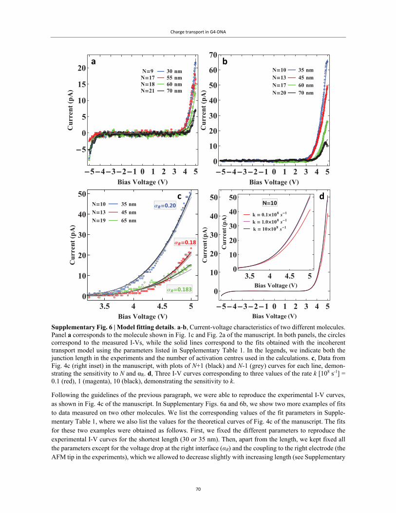
Charge transport in G4‐DNA
70
Supplementary Fig. 6 | Model fitting details. a-b, Current-voltage characteristics of two different molecules. Panel a corresponds to the molecule shown in Fig. 1c and Fig. 2a of the manuscript. In both panels, the circles correspond to the measured I-Vs, while the solid lines correspond to the fits obtained with the incoherent transport model using the parameters listed in Supplementary Table 1. In the legends, we indicate both the junction length in the experiments and the number of activation centres used in the calculations. c, Data from Fig. 4c (right inset) in the manuscript, with plots of N+1 (black) and N-1 (grey) curves for each line, demon-strating the sensitivity to N and αR. d, Three I-V curves corresponding to three values of the rate k [108 s-1] = 0.1 (red), 1 (magenta), 10 (black), demonstrating the sensitivity to k.
Following the guidelines of the previous paragraph, we were able to reproduce the experimental I-V curves, as shown in Fig. 4c of the manuscript. In Supplementary Figs. 6a and 6b, we show two more examples of fits to data measured on two other molecules. We list the corresponding values of the fit parameters in Supple-mentary Table 1, where we also list the values for the theoretical curves of Fig. 4c of the manuscript. The fits for these two examples were obtained as follows. First, we fixed the different parameters to reproduce the experimental I-V curves for the shortest length (30 or 35 nm). Then, apart from the length, we kept fixed all the parameters except for the voltage drop at the right interface (αR) and the coupling to the right electrode (the AFM tip in the experiments), which we allowed to decrease slightly with increasing length (see Supplementary
54321 0 1 2 3 4 5
0
10
20
30
40
50
Bias Voltage V
CurrentpA
c d
54321 0 1 2 3 4 5
0
10
20
30
40
50
60
70
Bias Voltage V
CurrentpA
35 nm
45 nm
60 nm
70 nm
N10N13N17N20
a b
54321 0 1 2 3 4 5
5
0
5
10
15
20
Bias Voltage V
CurrentpA
30 nm
55 nm
60 nm
70 nm
N9N17N18N21
3.5 4 4.5 50
10
20
30
40
50
Bias Voltage V
CurrentpA
N10
k 0.1108 s1
k 1.0108 s1
k 10108 s1
3.5 4 4.5 5
0
10
20
30
40
50
Bias Voltage V
CurrentpA
35 nm
45 nm
65 nm
N10
N13
N19
ΑR0.20
ΑR0.18
ΑR0.183
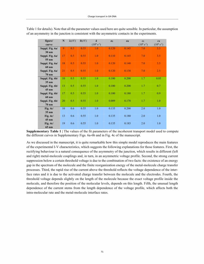
Charge transport in G4‐DNA
71
Table 1 for details). Note that all the parameter values used here are quite sensible. In particular, the assumption of an asymmetry in the junction is consistent with the asymmetric contacts in the experiments.
figure/ curve
N λ(eV) δ(eV) k (108 s-1)
αL
αR
cL
(108 s-1)
cR
(108 s-1)
Suppl. Fig. 6a/ 30 nm
9 0.5 0.55 1.0 0.120 0.145 7.0 3.5
Suppl. Fig. 6a/ 55 nm
17 0.5 0.55 1.0 0.110 0.145 7.0 3.5
Suppl. Fig. 6a/ 60 nm
18 0.5 0.55 1.0 0.120 0.140 7.0 3.5
Suppl. Fig. 6a/ 70 nm
21 0.5 0.55 1.0 0.120 0.138 7.0 2.5
Suppl. Fig. 6b/ 35 nm
10 0.5 0.55 1.0 0.100 0.200 1.7 0.85
Suppl. Fig. 6b/ 45 nm
13 0.5 0.55 1.0 0.100 0.200 1.7 0.7
Suppl. Fig. 6b/ 60 nm
17 0.5 0.55 1.0 0.100 0.180 1.7 0.9
Suppl. Fig. 6b/ 70 nm
20 0.5 0.55 1.0 0.009 0.170 1.7 1.0
Fig. 4c/ 35 nm
10 0.6 0.55 1.0 0.135 0.200 2.0 1.0
Fig. 4c/ 45 nm
13 0.6 0.55 1.0 0.135 0.180 2.0 1.0
Fig. 4c/ 65 nm
19 0.6 0.55 1.0 0.135 0.183 2.0 1.0
Supplementary Table 1 | The values of the fit parameters of the incoherent transport model used to compute the different curves in Supplementary Figs. 6a-6b and in Fig. 4c of the manuscript.
As we discussed in the manuscript, it is quite remarkable how this simple model reproduces the main features of the experimental I-V characteristics, which suggests the following explanations for those features. First, the rectifying behaviour is a natural consequence of the asymmetry of the junction, which results in different (left and right) metal-molecule couplings and, in turn, in an asymmetric voltage profile. Second, the strong current suppression below a certain threshold voltage is due to the combination of two facts: the existence of an energy gap in the spectrum of the molecule and the finite reorganization energy of the metal-molecule charge transfer processes. Third, the rapid rise of the current above the threshold reflects the voltage dependence of the inter-face rates and it is due to the activated charge transfer between the molecule and the electrodes. Fourth, the threshold voltage depends slightly on the length of the molecule because the exact voltage profile inside the molecule, and therefore the position of the molecular levels, depends on this length. Fifth, the unusual length dependence of the current stems from the length dependence of the voltage profile, which affects both the intra-molecular rate and the metal-molecule interface rates.
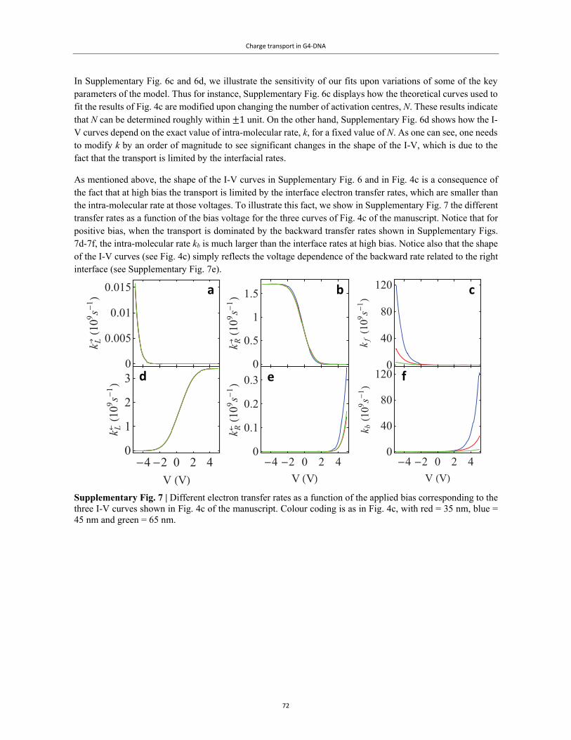
Charge transport in G4‐DNA
72
In Supplementary Fig. 6c and 6d, we illustrate the sensitivity of our fits upon variations of some of the key parameters of the model. Thus for instance, Supplementary Fig. 6c displays how the theoretical curves used to fit the results of Fig. 4c are modified upon changing the number of activation centres, N. These results indicate that N can be determined roughly within 1 unit. On the other hand, Supplementary Fig. 6d shows how the I-V curves depend on the exact value of intra-molecular rate, k, for a fixed value of N. As one can see, one needs to modify k by an order of magnitude to see significant changes in the shape of the I-V, which is due to the fact that the transport is limited by the interfacial rates.
As mentioned above, the shape of the I-V curves in Supplementary Fig. 6 and in Fig. 4c is a consequence of the fact that at high bias the transport is limited by the interface electron transfer rates, which are smaller than the intra-molecular rate at those voltages. To illustrate this fact, we show in Supplementary Fig. 7 the different transfer rates as a function of the bias voltage for the three curves of Fig. 4c of the manuscript. Notice that for positive bias, when the transport is dominated by the backward transfer rates shown in Supplementary Figs. 7d-7f, the intra-molecular rate kb is much larger than the interface rates at high bias. Notice also that the shape of the I-V curves (see Fig. 4c) simply reflects the voltage dependence of the backward rate related to the right interface (see Supplementary Fig. 7e).
Supplementary Fig. 7 | Different electron transfer rates as a function of the applied bias corresponding to the three I-V curves shown in Fig. 4c of the manuscript. Colour coding is as in Fig. 4c, with red = 35 nm, blue = 45 nm and green = 65 nm.
0
0.005
0.01
0.015
k L109s1
42 0 2 40
1
2
3
V V
k L109s1
0
0.5
1
1.5
k R109s1
4 2 0 2 40
0.1
0.2
0.3
V V
k R109s1
0
40
80
120
k f109s1
4 2 0 2 40
40
80
120
V V
k b109s1
a b c
d e f
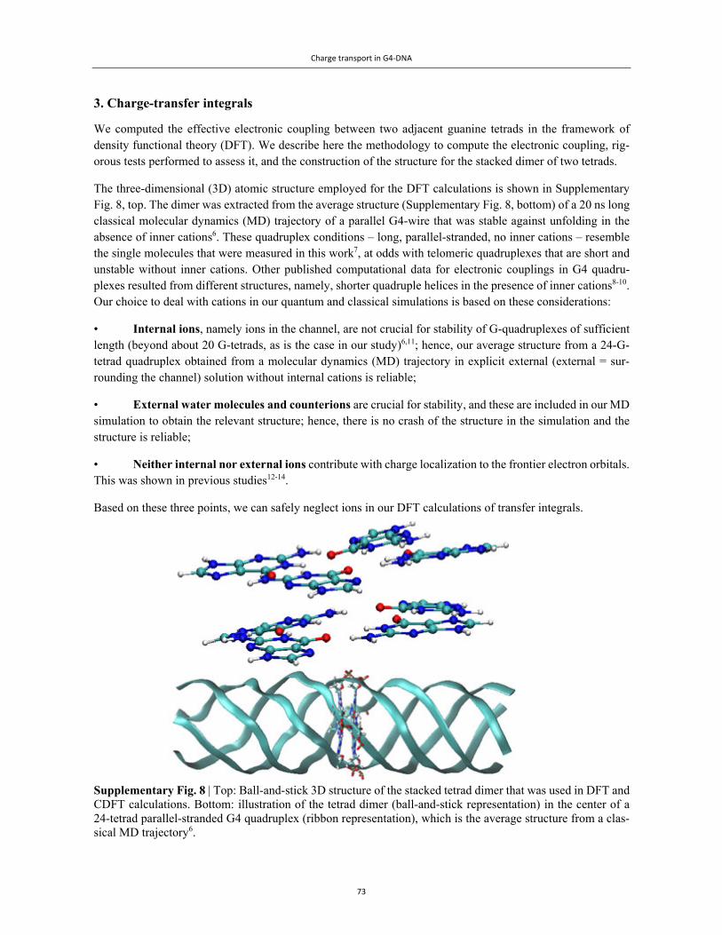
Charge transport in G4‐DNA
73
3. Charge-transfer integrals
We computed the effective electronic coupling between two adjacent guanine tetrads in the framework of density functional theory (DFT). We describe here the methodology to compute the electronic coupling, rig-orous tests performed to assess it, and the construction of the structure for the stacked dimer of two tetrads.
The three-dimensional (3D) atomic structure employed for the DFT calculations is shown in Supplementary Fig. 8, top. The dimer was extracted from the average structure (Supplementary Fig. 8, bottom) of a 20 ns long classical molecular dynamics (MD) trajectory of a parallel G4-wire that was stable against unfolding in the absence of inner cations6. These quadruplex conditions – long, parallel-stranded, no inner cations – resemble the single molecules that were measured in this work7, at odds with telomeric quadruplexes that are short and unstable without inner cations. Other published computational data for electronic couplings in G4 quadru-plexes resulted from different structures, namely, shorter quadruple helices in the presence of inner cations8-10. Our choice to deal with cations in our quantum and classical simulations is based on these considerations:
• Internal ions, namely ions in the channel, are not crucial for stability of G-quadruplexes of sufficient length (beyond about 20 G-tetrads, as is the case in our study)6,11; hence, our average structure from a 24-G-tetrad quadruplex obtained from a molecular dynamics (MD) trajectory in explicit external (external = sur-rounding the channel) solution without internal cations is reliable;
• External water molecules and counterions are crucial for stability, and these are included in our MD simulation to obtain the relevant structure; hence, there is no crash of the structure in the simulation and the structure is reliable;
• Neither internal nor external ions contribute with charge localization to the frontier electron orbitals. This was shown in previous studies12-14.
Based on these three points, we can safely neglect ions in our DFT calculations of transfer integrals.
Supplementary Fig. 8 | Top: Ball-and-stick 3D structure of the stacked tetrad dimer that was used in DFT and CDFT calculations. Bottom: illustration of the tetrad dimer (ball-and-stick representation) in the center of a 24-tetrad parallel-stranded G4 quadruplex (ribbon representation), which is the average structure from a clas-sical MD trajectory6.
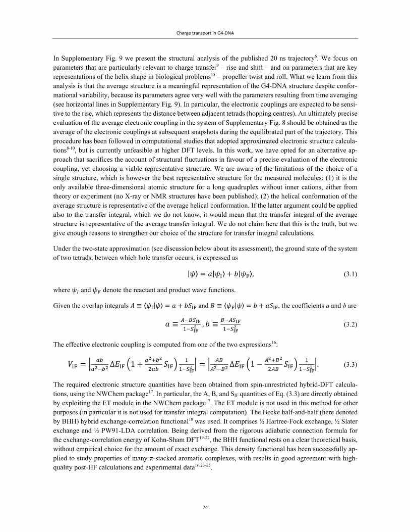
Charge transport in G4‐DNA
74
In Supplementary Fig. 9 we present the structural analysis of the published 20 ns trajectory6. We focus on parameters that are particularly relevant to charge transfer9 – rise and shift – and on parameters that are key representations of the helix shape in biological problems15 – propeller twist and roll. What we learn from this analysis is that the average structure is a meaningful representation of the G4-DNA structure despite confor-mational variability, because its parameters agree very well with the parameters resulting from time averaging (see horizontal lines in Supplementary Fig. 9). In particular, the electronic couplings are expected to be sensi-tive to the rise, which represents the distance between adjacent tetrads (hopping centres). An ultimately precise evaluation of the average electronic coupling in the system of Supplementary Fig. 8 should be obtained as the average of the electronic couplings at subsequent snapshots during the equilibrated part of the trajectory. This procedure has been followed in computational studies that adopted approximated electronic structure calcula-tions8-10, but is currently unfeasible at higher DFT levels. In this work, we have opted for an alternative ap-proach that sacrifices the account of structural fluctuations in favour of a precise evaluation of the electronic coupling, yet choosing a viable representative structure. We are aware of the limitations of the choice of a single structure, which is however the best representative structure for the measured molecules: (1) it is the only available three-dimensional atomic structure for a long quadruplex without inner cations, either from theory or experiment (no X-ray or NMR structures have been published); (2) the helical conformation of the average structure is representative of the average helical conformation. If the latter argument could be applied also to the transfer integral, which we do not know, it would mean that the transfer integral of the average structure is representative of the average transfer integral. We do not claim here that this is the truth, but we give enough reasons to strengthen our choice of the structure for transfer integral calculations.
Under the two-state approximation (see discussion below about its assessment), the ground state of the system of two tetrads, between which hole transfer occurs, is expressed as
| | | , (3.1)
where and denote the reactant and product wave functions.
Given the overlap integrals ≡ | and ≡ | , the coefficients a and b are
≡ , ≡ (3.2)
The effective electronic coupling is computed from one of the two expressions16:
∆ 1 ∆ 1 . (3.3)
The required electronic structure quantities have been obtained from spin-unrestricted hybrid-DFT calcula-tions, using the NWChem package17. In particular, the A, B, and SIF quantities of Eq. (3.3) are directly obtained by exploiting the ET module in the NWChem package17. The ET module is not used in this method for other purposes (in particular it is not used for transfer integral computation). The Becke half-and-half (here denoted by BHH) hybrid exchange-correlation functional18 was used. It comprises ½ Hartree-Fock exchange, ½ Slater exchange and ½ PW91-LDA correlation. Being derived from the rigorous adiabatic connection formula for the exchange-correlation energy of Kohn-Sham DFT19-22, the BHH functional rests on a clear theoretical basis, without empirical choice for the amount of exact exchange. This density functional has been successfully ap-plied to study properties of many π-stacked aromatic complexes, with results in good agreement with high-quality post-HF calculations and experimental data16,23-25.
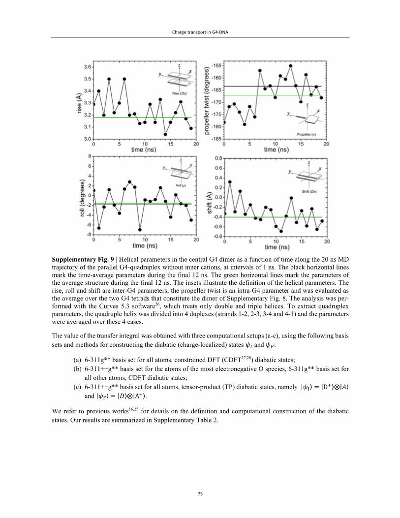
Charge transport in G4‐DNA
75
Supplementary Fig. 9 | Helical parameters in the central G4 dimer as a function of time along the 20 ns MD trajectory of the parallel G4-quadruplex without inner cations, at intervals of 1 ns. The black horizontal lines mark the time-average parameters during the final 12 ns. The green horizontal lines mark the parameters of the average structure during the final 12 ns. The insets illustrate the definition of the helical parameters. The rise, roll and shift are inter-G4 parameters; the propeller twist is an intra-G4 parameter and was evaluated as the average over the two G4 tetrads that constitute the dimer of Supplementary Fig. 8. The analysis was per-formed with the Curves 5.3 software26, which treats only double and triple helices. To extract quadruplex parameters, the quadruple helix was divided into 4 duplexes (strands 1-2, 2-3, 3-4 and 4-1) and the parameters were averaged over these 4 cases.
The value of the transfer integral was obtained with three computational setups (a-c), using the following basis sets and methods for constructing the diabatic (charge-localized) states and :
(a) 6-311g** basis set for all atoms, constrained DFT (CDFT27,28) diabatic states; (b) 6-311++g** basis set for the atoms of the most electronegative O species, 6-311g** basis set for
all other atoms, CDFT diabatic states; (c) 6-311++g** basis set for all atoms, tensor-product (TP) diabatic states, namely | |D ⨂|
and | | ⨂|A .
We refer to previous works16,25 for details on the definition and computational construction of the diabatic states. Our results are summarized in Supplementary Table 2.
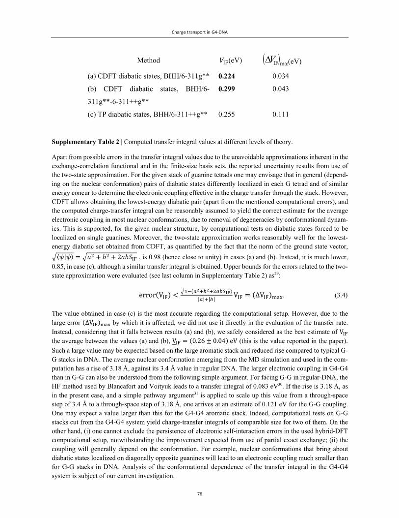
Charge transport in G4‐DNA
76
Method (eV) maxIFV (eV)
(a) CDFT diabatic states, BHH/6-311g** 0.224 0.034
(b) CDFT diabatic states, BHH/6-
311g**-6-311++g**
0.299 0.043
(c) TP diabatic states, BHH/6-311++g** 0.255 0.111
Supplementary Table 2 | Computed transfer integral values at different levels of theory.
Apart from possible errors in the transfer integral values due to the unavoidable approximations inherent in the exchange-correlation functional and in the finite-size basis sets, the reported uncertainty results from use of the two-state approximation. For the given stack of guanine tetrads one may envisage that in general (depend-ing on the nuclear conformation) pairs of diabatic states differently localized in each G tetrad and of similar energy concur to determine the electronic coupling effective in the charge transfer through the stack. However, CDFT allows obtaining the lowest-energy diabatic pair (apart from the mentioned computational errors), and the computed charge-transfer integral can be reasonably assumed to yield the correct estimate for the average electronic coupling in most nuclear conformations, due to removal of degeneracies by conformational dynam-ics. This is supported, for the given nuclear structure, by computational tests on diabatic states forced to be localized on single guanines. Moreover, the two-state approximation works reasonably well for the lowest-energy diabatic set obtained from CDFT, as quantified by the fact that the norm of the ground state vector,
| 2 , is 0.98 (hence close to unity) in cases (a) and (b). Instead, it is much lower,
0.85, in case (c), although a similar transfer integral is obtained. Upper bounds for the errors related to the two-state approximation were evaluated (see last column in Supplementary Table 2) as29:
error V| | | |
V ∆V . (3.4)
The value obtained in case (c) is the most accurate regarding the computational setup. However, due to the large error ∆V by which it is affected, we did not use it directly in the evaluation of the transfer rate. Instead, considering that it falls between results (a) and (b), we safely considered as the best estimate of V the average between the values (a) and (b), V 0.26 0.04 eV (this is the value reported in the paper).
Such a large value may be expected based on the large aromatic stack and reduced rise compared to typical G-G stacks in DNA. The average nuclear conformation emerging from the MD simulation and used in the com-putation has a rise of 3.18 Å, against its 3.4 Å value in regular DNA. The larger electronic coupling in G4-G4 than in G-G can also be understood from the following simple argument. For facing G-G in regular-DNA, the HF method used by Blancafort and Voityuk leads to a transfer integral of 0.083 eV30. If the rise is 3.18 Å, as in the present case, and a simple pathway argument31 is applied to scale up this value from a through-space step of 3.4 Å to a through-space step of 3.18 Å, one arrives at an estimate of 0.121 eV for the G-G coupling. One may expect a value larger than this for the G4-G4 aromatic stack. Indeed, computational tests on G-G stacks cut from the G4-G4 system yield charge-transfer integrals of comparable size for two of them. On the other hand, (i) one cannot exclude the persistence of electronic self-interaction errors in the used hybrid-DFT computational setup, notwithstanding the improvement expected from use of partial exact exchange; (ii) the coupling will generally depend on the conformation. For example, nuclear conformations that bring about diabatic states localized on diagonally opposite guanines will lead to an electronic coupling much smaller than for G-G stacks in DNA. Analysis of the conformational dependence of the transfer integral in the G4-G4 system is subject of our current investigation.
Charge transport in G4‐DNA
77
Charge-transfer integral values of the same order of magnitude as our outcome (and up to a value of 0.4 eV) have been obtained, depending on structural parameters8. Significantly smaller values have also been obtained for short G4-G4 strands that contain monovalent alkali ions and show significantly larger rises10. The transfer integrals reported in Supplementary Table 2 of a very recent work9 demonstrate high sensitivity of the elec-tronic coupling to the structure32. The fact that we adopted a structure with a rather small rise for the parallel long G4-quadruplex of this study is likely the origin of our large value of the transfer integral. This outcome is not an artefact, but a consequence of the very peculiar structure of the G4-quadruplexes used in the experi-ments.
4. Charge-transfer mechanism
In this section, we use the computed transfer integral to estimate the value of the intra-molecular transfer rate and to shed some light on the charge transfer mechanism.
The Landau-Zener result for the probability of electron transfer from the diabatic Born-Oppenheimer surface of a Donor (I) to that of an acceptor A (F) is
→ 1 exp , (4.1)
where
⁄,
, (4.2)
is the Landau-Zener parameter32-35. in Eq. (4.2) is the average phonon frequency of “classical” phonons that trigger the electron transfer activation step, λ , is the total reorganization energy and V is the electronic
coupling between initial (donor) and final (acceptor) states. For classical phonons sec.
If 1, the ET rate is non-adiabatic (superscript nad), given by
,,
, exp ∆, (4.3)
with activation energy
∆∆ , ,
,, (4.4)
where ∆ , is the free energy gap of the reaction.
If 1 the rate is adiabatic (superscript ad) and largely independent of the electronic coupling:
, exp∆ act
ad
, 1 (4.5)
with ∆ ∆ .
In the limit ∆ , 0, we have
∆ λF,I 4⁄ , ∆ λF,I 4⁄ V , . (4.6)
In the more general case of a finite value of ∆ , , we have
Charge transport in G4‐DNA
78
∆∆ , ,
,, ∆
∆ , ,
,V , . (4.7)
Further, we distinguish between the “localized” and “delocalized” polaron regimes. According to polaron the-ory, a polaron-like electronic wave function is localized at one of two sites coupled with electronic coupling
V , if V , E , where E ∆ , λ , 4⁄ λ , is the polaron binding energy (if ∆ , 0, Eλ , 4⁄ ). In the localized polaron regime, the initial state of a hopping step is localized within a G4 tetrad and
the final state is localized in the adjacent G4 tetrad. In the delocalized regime, the initial and final states can be delocalized over several G4 tetrads and the values of the electronic coupling and reorganization energy that enter the formula for the charge transfer rate need to be renormalized by the number of sites.
This formalism sets the framework for the relation between the ab initio computed value of the electronic coupling, V , 0.26eV, and the value of the transfer rate obtained from the model fit of the experimental
data. Knowledge of V , and λ , fixes the transport regime and one can evaluate the transfer rate accordingly.
We first consider the charge transfer mechanisms by embracing the DFT prediction of the electronic coupling and the fit value of the reorganization energy. In a second instance, we relax this condition and consider other possibilities.
The model fit yields an interfacial reorganization energy (e.g., at the electrode junctions) of 0.5 eV, which corresponds to an intra-molecular reorganization energy of at least 1 eV36. V , 0.26eV is very close to the
polaron binding energy for a reasonably small or negligible value of the free energy gap of the reaction, which
means that we are in a borderline regime between localized and delocalized polarons (V , E if ∆ , is
larger than 2 meV).
Let us hypothesize a delocalized polaron regime in which the initial (final) polaron state is delocalized over M G4 tetrads. Then the effective electronic coupling for the charge transfer reaction should be obtained as 1/M of the inter-tetrad coupling, with the same factor for the reorganization energy. The Landau-Zener parameter becomes
⁄
⁄,
, , (4.8)
where V , 0.26eV is the computed electronic coupling and λ , 1eV is the fitted reorganization energy
for inter-tetrad charge transfer. For M = 10 (SI section 2), 0.075 eV⁄ . For the rate to be nonadiabatic ( 1) we need 0.075eV. 0.075eV corresponds to typical bond angle vibrations with periods of tens of femtoseconds. So 0.075eV means that the average period of the motions that trigger electron transfer be less than tens of femtoseconds. This is a very high frequency, not typical of “classical” phonons and therefore we expect 1, namely adiabatic charge transfer. The adiabatic activation energy computed with Eq. (4.7) using renormalized values of the electronic coupling and reorganization energy exceeds the thermal energy if ∆ , is larger than 44 meV. This means that for even a small reaction free energy gap
(roughly larger than 20 meV, which is of the order of ) the process is adiabatic and activated. In such a condition, the rate can be computed through Eq. (4.5). For example, assuming ∆G , 0.2eV, we obtain
∆G 0.2eV and the transfer rate through Eq. (4.5) is , 0.5 10 . Using the “classical” phonon
frequency sec,the transfer integral is , 0.5 10 that agrees with the estimate from the model
fit. Even if we consider smaller values of ∆ , , as small as about 0.1 eV, the agreement is still qualitatively
good.
Charge transport in G4‐DNA
79
If, instead, the charge transfer in our system involves localized polarons, then 2.38 eV⁄ and for viable phonon frequencies, the regime is adiabatic also in such conditions. The adiabatic activation energy computed with Eq. (4.7) using the calculated and fitted values of the electronic coupling and reorganization
energy, respectively, is positive if ∆ , is larger than 20 meV. Assuming ∆ , 0.2eV, we obtain ∆G
0.1eV and the transfer rate through Eq. (4.5) is , 3.0 10 . Using the “classical” phonon fre-
quency sec, the inter-tetrad transfer integral yields , 3.0 10 sec . This value should be di-
vided by ~10-100 to extract the transfer rate over 10 tetrads for comparison to the model transfer rate that has been fitted for a distance of about 3.5 nm: this is again a fair agreement.
In summary, bestowing our DFT transfer integrals and the reorganization energy and transfer rate estimated from the model fit, if charge transfer in our system occurs with an activation free energy gap in the range of 1-2 tens of eV (which is not unreasonable considering the asymmetric measurement conditions and many un-known structural features) the process is adiabatic, compatible with either localized or delocalized polarons. If the reaction free energy gap is rigorously zero, the adiabatic activation energy is negative and the phenomenon is in the limit of band transport, which would be strongly affected by defects and cannot be formulated at this stage, considering the many unknowns of the system structure.
Let us briefly comment on alternative explanations. As we noted above, we suggest that the structures used in this experimental work are peculiar and yield a high transfer integral of 0.26 eV that is compatible with the model. Yet, we wish to estimate the transfer mechanism taking into account other published results for both the transfer integral and reorganization energy.
Given the lack of knowledge of the conformational ensemble and the environment of the G4-DNA molecule in the experiment, it is fair to consider different scenarios. Semi-empirical computations for a large number of G4 dimers taken from MD simulations show large variability of the inter-tetrad electronic coupling V , with
changes in structural conformation, ranging from maximum values of a few tens of an eV to average values of hundredths of an eV (e.g., rms V , 0.05eV)9,10. More uncertainties plague the reorganization energy because
in the case of G4-DNA this quantity has not been computed. We now consider a range of values used for guanine-to-guanine hopping in the literature on hole transfer in DNA, where the minimum values refer to the inner sphere reorganization energy and the maximum values to the total reorganization energy (0.7eV ,
1.4eV .
With a small electronic coupling V , 0.05eV and λ , 0.7 1.4eV we have V , . In this condi-
tion, the hopping steps must involve localized polarons in adjacent G4 tetrads. With V , 0.05eV and ,
0.7 1.4eV, 0.07 0.1 eV⁄ [Eq. (4.2)]. Assuming again, that charge transfer is promoted by classical modes, we expect ≪ 0.1eV. Therefore, 1 and the adiabatic regime is relevant to the near-est-neighbor hopping rate in the localized polaron limit. Using Eqs. (4.5) and (4.6) with zero reaction free energy gap, we estimate , 10 for , 1.4eV and , 10 for , 0.7eV. Setting
sec gives , 10 sec for , 1.4eV and , 10 sec for , 0.7eV. The results of
the hopping model simulations (see section) give a value of 10 sec for the effective unbiased rate between sites i and i+10 (with an uncertainty of an order of magnitude). If this rate is interpreted as arising from approximately 10 nearest-neighbor hopping steps then the nearest-neighbor unbiased hopping rate should be 100 10 sec (assuming diffusive transport for the unbiased rate)36. Therefore, for an average cou-pling of few hundreds of an eV the hopping model prediction is more consistent with reorganization energies closer to the 0.7 eV value limit.
On the other hand, a reorganization energy , 1.4eV at the higher limit of the considered interval pertains
to G-G dimers. Using it in Equations 4.3-4.7 with our DFT electronic coupling V 0.26eV, we obtain a
Charge transport in G4‐DNA
80
picture that is compatible with the regime of a localized polaron on one G4 tetrad. In such conditions 2 eV⁄ and the rate is strongly adiabatic for classical phonons. Using Equations 4.5 and 4.6 with 1 and ∆ , 0 gives , 10 sec using sec. This inter-tetrad transfer rate is consistent with the
model fit of , 10 sec over ten tetrads, which means that a high value of the electronic coupling is
consistent with the whole picture even in the limit of a zero reaction free energy, provided that the reorganiza-tion energy is at the upper limit of the range estimated for dsDNA. A value of , 1.4eV is not in contrast
with the model fit , 1eV (inter-tetrad), considering the experimental errors and the simplicity of the
model.
5. References
1 Vazquez‐Mena, O. et al. Analysis of the blurring in stencil lithography. Nanotechnology 20, 415303 (2009). 2 Couderc, S., Blech, V. & Kim, B. New Surface Treatment and Microscale/Nanoscale Surface Patterning Using
Electrostatically Clamped Stencil Mask. Jpn J Appl Phys 48 (2009). 3 Polizzi, N. F., Skourtis, S. S. & Beratan, D. N. Physical constraints on charge transport through bacterial nan‐
owires. Faraday Discuss 155, 43‐62 (2012). 4 Lehmann, J., Ingold, G. L. & Hanggi, P. Incoherent charge transport through molecular wires: interplay of Cou‐
lomb interaction and wire population. Chem Phys 281, 199‐209 (2002). 5 Chidsey, C. E. D. Free‐Energy and Temperature‐Dependence of Electron‐Transfer at the Metal‐Electrolyte In‐
terface. Science 251, 919‐922 (1991). 6 Cavallari, M., Calzolari, A., Garbesi, A. & Di Felice, R. Stability and migration of metal ions in G4‐wires by mo‐
lecular dynamics simulations. J Phys Chem B 110, 26337‐26348 (2006). 7 Borovok, N. et al. Assembling of G‐strands into novel tetra‐molecular parallel G4‐DNA nanostructures using
avidinbiotin recognition. Nucleic Acids Res 36, 5050‐5060 (2008). 8 Kubar, T., Woiczikowski, P. B., Cuniberti, G. & Elstner, M. Efficient calculation of charge‐transfer matrix ele‐
ments for hole transfer in DNA. J Phys Chem B 112, 7937‐7947 (2008). 9 Lech, C. J., Phan, A. T., Michel‐Beyerle, M. E. & Voityuk, A. A. Electron‐Hole Transfer in G‐Quadruplexes with
Different Tetrad Stacking Geometries: A Combined QM and MD Study. J Phys Chem B 117, 9851‐9856 (2013). 10 Woiczikowski, P. B., Kubar, T., Gutierrez, R., Cuniberti, G. & Elstner, M. Structural stability versus conforma‐
tional sampling in biomolecular systems: Why is the charge transfer efficiency in G4‐DNA better than in dou‐ble‐stranded DNA? J Chem Phys 133, 035103 (2010).
11 Kotlyar, A. B. et al. Long, monomolecular guanine‐based nanowires. Adv Mater 17, 1901‐1904 (2005). 12 de Pablo, P. J. et al. Absence of dc‐conductivity in lambda‐DNA. Phys Rev Lett 85, 4992‐4995 (2000). 13 Barnett, R. N., Cleveland, C. L., Joy, A., Landman, U. & Schuster, G. B. Charge migration in DNA: Ion‐gated
transport. Science 294, 567‐571 (2001). 14 Calzolari, A., Di Felice, R., Molinari, E. & Garbesi, A. Electron channels in biomolecular nanowires. J Phys Chem
B 108, 2509‐2515 (2004). 15 Zhou, T. Y. et al. DNAshape: a method for the high‐throughput prediction of DNA structural features on a ge‐
nomic scale. Nucleic Acids Res 41, W56‐W62 (2013). 16 Migliore, A. Full‐electron calculation of effective electronic couplings and excitation energies of charge trans‐
fer states: Application to hole transfer in DNA pi‐stacks. J Chem Phys 131, 114113 (2009). 17 Valiev, M. et al. NWChem: A comprehensive and scalable open‐source solution for large scale molecular sim‐
ulations. Comput Phys Commun 181, 1477‐1489 (2010). 18 Becke, A. D. A New Mixing of Hartree‐Fock and Local Density‐Functional Theories. J Chem Phys 98, 1372‐1377
(1993). 19 Harris, J. & Jones, R. O. Surface‐Energy of a Bounded Electron‐Gas. J Phys F Met Phys 4, 1170‐1186 (1974). 20 Gunnarsson, O. & Lundqvist, B. I. Exchange and Correlation in Atoms, Molecules, and Solids by Spin‐Density
Functional Formalism. Phys Rev B 13, 4274‐4298 (1976). 21 Langreth, D. C. & Perdew, J. P. Exchange‐Correlation Energy of a Metallic Surface ‐ Wave‐Vector Analysis.
Phys Rev B 15, 2884‐2901 (1977). 22 Harris, J. Adiabatic‐Connection Approach to Kohn‐Sham Theory. Phys Rev A 29, 1648‐1659 (1984). 23 Waller, M. P., Robertazzi, A., Platts, J. A., Hibbs, D. E. & Williams, P. A. Hybrid density functional theory for pi‐
stacking interactions: Application to benzenes, pyridines, and DNA bases. J Comput Chem 27, 491‐504 (2006).
Charge transport in G4‐DNA
81
24 Miura, M., Aoki, Y. & Champagne, B. Assessment of time‐dependent density functional schemes for compu‐ting the oscillator strengths of benzene, phenol, aniline, and fluorobenzene. J Chem Phys 127 (2007).
25 Migliore, A. Nonorthogonality Problem and Effective Electronic Coupling Calculation: Application to Charge Transfer in pi‐Stacks Relevant to Biochemistry and Molecular Electronics. J Chem Theory Comput 7, 1712‐1725 (2011).
26 Lavery, R. & Sklenar, H. Defining the Structure of Irregular Nucleic‐Acids ‐ Conventions and Principles. J Bio‐mol Struct Dyn 6, 655‐667 (1989).
27 Wu, Q. & Van Voorhis, T. Direct optimization method to study constrained systems within density‐functional theory. Phys Rev A 72 (2005).
28 Wu, Q. & Van Voorhis, T. Extracting electron transfer coupling elements from constrained density functional theory. J Chem Phys 125 (2006).
29 Migliore, A., Corni, S., Di Felice, R. & Molinari, E. First‐principles density‐functional theory calculations of elec‐tron‐transfer rates in azurin dimers. J Chem Phys 124 (2006).
30 Rosch, N. & Voityuk, A. A. Quantum chemical calculation of donor‐acceptor coupling for charge transfer in DNA. Top Curr Chem 237, 37‐72 (2004).
31 Beratan, D. N., Betts, J. N. & Onuchic, J. N. Tunneling Pathway and Redox‐State‐Dependent Electronic Cou‐plings at Nearly Fixed Distance in Electron‐Transfer Proteins. J Phys Chem‐Us 96, 2852‐2855 (1992).
32 Skourtis, S. S., Waldeck, D. H. & Beratan, D. N. Fluctuations in Biological and Bioinspired Electron‐Transfer Reactions. Annu Rev Phys Chem 61, 461‐485 (2010).
33 Sumi, H. in Electron Transfer in Chemistry (Wiley‐VCH Press, 2001). 34 Landau, L. Zur Theorie der Energieubertragung. II. Physikalische Zeitschrift der Sowjetunion 2, 46‐51 (1932). 35 Zener, C. Non‐Adiabatic Crossing of Energy Levels. Proceedings of the Royal Society of London A 137, 696‐702
(1932). 36 Nitzan, A. Chemical Dynamics in Condensed Phases. (Oxford University Press, 2006).
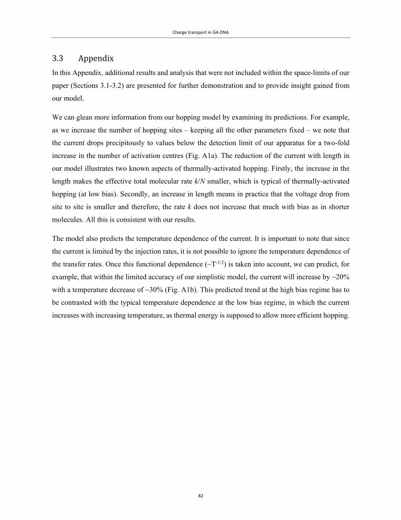
Charge transport in G4‐DNA
82
3.3 Appendix
In this Appendix, additional results and analysis that were not included within the space-limits of our
paper (Sections 3.1-3.2) are presented for further demonstration and to provide insight gained from
our model.
We can glean more information from our hopping model by examining its predictions. For example,
as we increase the number of hopping sites – keeping all the other parameters fixed – we note that
the current drops precipitously to values below the detection limit of our apparatus for a two-fold
increase in the number of activation centres (Fig. A1a). The reduction of the current with length in
our model illustrates two known aspects of thermally-activated hopping. Firstly, the increase in the
length makes the effective total molecular rate k/N smaller, which is typical of thermally-activated
hopping (at low bias). Secondly, an increase in length means in practice that the voltage drop from
site to site is smaller and therefore, the rate k does not increase that much with bias as in shorter
molecules. All this is consistent with our results.
The model also predicts the temperature dependence of the current. It is important to note that since
the current is limited by the injection rates, it is not possible to ignore the temperature dependence of
the transfer rates. Once this functional dependence (~T-1/2) is taken into account, we can predict, for
example, that within the limited accuracy of our simplistic model, the current will increase by ~20%
with a temperature decrease of ~30% (Fig. A1b). This predicted trend at the high bias regime has to
be contrasted with the typical temperature dependence at the low bias regime, in which the current
increases with increasing temperature, as thermal energy is supposed to allow more efficient hopping.
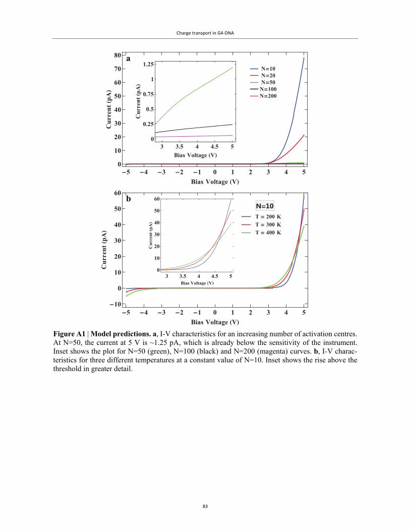
Charge transport in G4‐DNA
83
Figure A1 | Model predictions. a, I-V characteristics for an increasing number of activation centres. At N=50, the current at 5 V is ~1.25 pA, which is already below the sensitivity of the instrument. Inset shows the plot for N=50 (green), N=100 (black) and N=200 (magenta) curves. b, I-V charac-teristics for three different temperatures at a constant value of N=10. Inset shows the rise above the threshold in greater detail.
5 4 3 2 1 0 1 2 3 4 5
0
10
20
30
40
50
60
70
80
Bias Voltage V
CurrentpA
N10N20N50N100N200
a
3 3.5 4 4.5 5
0
0.25
0.5
0.75
1
1.25
Bias Voltage V
CurrentpA
3 3.5 4 4.5 5
0
10
20
30
40
50
60
Bias Voltage V
CurrentpA
5 4 3 2 1 0 1 2 3 4 5
10
0
10
20
30
40
50
60
Bias Voltage V
CurrentpA
N10T 200 KT 300 KT 400 K
b
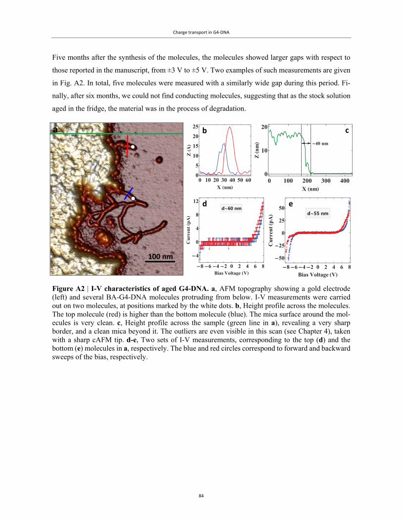
Charge transport in G4‐DNA
84
Five months after the synthesis of the molecules, the molecules showed larger gaps with respect to
those reported in the manuscript, from ±3 V to ±5 V. Two examples of such measurements are given
in Fig. A2. In total, five molecules were measured with a similarly wide gap during this period. Fi-
nally, after six months, we could not find conducting molecules, suggesting that as the stock solution
aged in the fridge, the material was in the process of degradation.
Figure A2 | I-V characteristics of aged G4-DNA. a, AFM topography showing a gold electrode (left) and several BA-G4-DNA molecules protruding from below. I-V measurements were carried out on two molecules, at positions marked by the white dots. b, Height profile across the molecules. The top molecule (red) is higher than the bottom molecule (blue). The mica surface around the mol-ecules is very clean. c, Height profile across the sample (green line in a), revealing a very sharp border, and a clean mica beyond it. The outliers are even visible in this scan (see Chapter 4), taken with a sharp cAFM tip. d-e, Two sets of I-V measurements, corresponding to the top (d) and the bottom (e) molecules in a, respectively. The blue and red circles correspond to forward and backward sweeps of the bias, respectively.
b
100 nm
a
0 100 200 300 4000
10
20
X nm
Znm 40 nm
0 10 20 30 40 50 600
5
10
15
20
25
X nmZ
c
8 6 4 2 0 2 4 6 8
4
0
4
8
12
Bias Voltage V
CurrentpA
d60 nmd e
8642 0 2 4 6 8
50
25
0
25
50
Bias Voltage VCurrentpA d55 nm
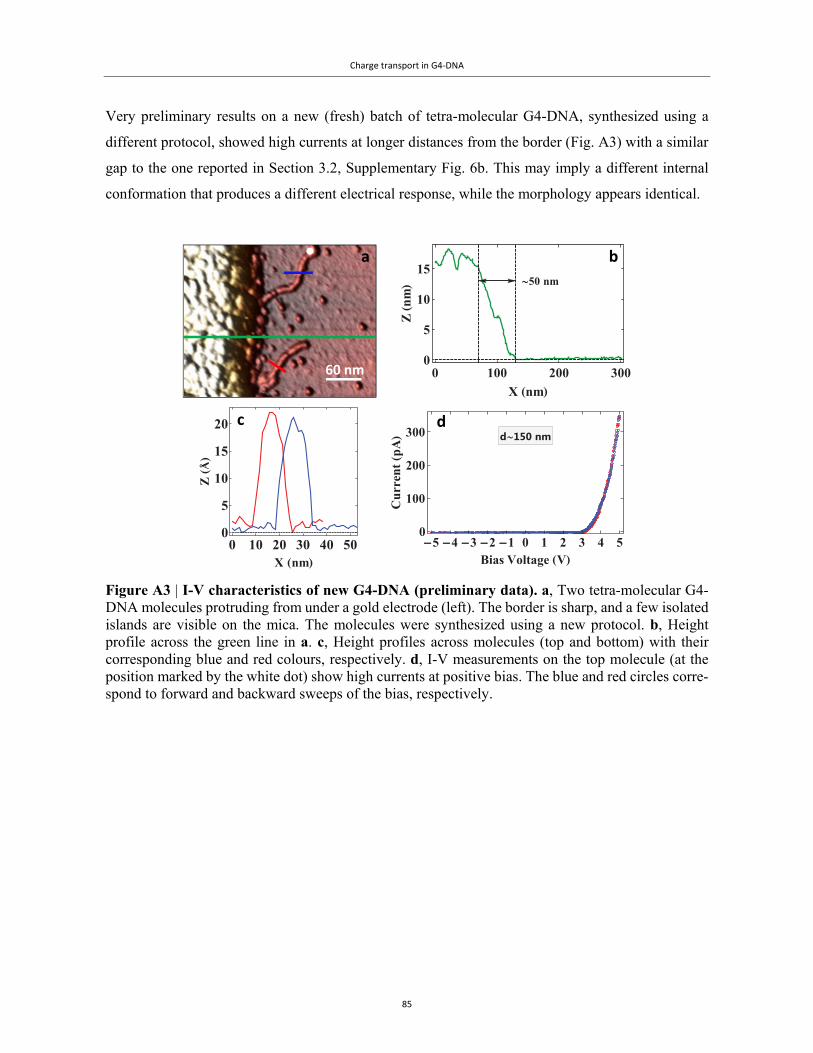
Charge transport in G4‐DNA
85
Very preliminary results on a new (fresh) batch of tetra-molecular G4-DNA, synthesized using a
different protocol, showed high currents at longer distances from the border (Fig. A3) with a similar
gap to the one reported in Section 3.2, Supplementary Fig. 6b. This may imply a different internal
conformation that produces a different electrical response, while the morphology appears identical.
Figure A3 | I-V characteristics of new G4-DNA (preliminary data). a, Two tetra-molecular G4-DNA molecules protruding from under a gold electrode (left). The border is sharp, and a few isolated islands are visible on the mica. The molecules were synthesized using a new protocol. b, Height profile across the green line in a. c, Height profiles across molecules (top and bottom) with their corresponding blue and red colours, respectively. d, I-V measurements on the top molecule (at the position marked by the white dot) show high currents at positive bias. The blue and red circles corre-spond to forward and backward sweeps of the bias, respectively.
60 nm
a b
c d
0 10 20 30 40 500
5
10
15
20
X nm
Z
0 100 200 3000
5
10
15
X nmZnm 50 nm
5 4 3 2 1 0 1 2 3 4 50
100
200
300
Bias Voltage V
CurrentpA d150 nm

87
Chemical‐freelithographywithna‐nometre‐precision via reversible electrostaticclampingTo be submitted (2014).
4.1 Mainmanuscript
Chemical-free lithography with nanometre-precision via reversible electrostatic clamping
Gideon I. Livshits1,2, Eduard M. Mastov1, Inna Popov2, David S. Livshits3, Roman Zhuravel1,2, Peter Kjær Kristensen4, Dvir Rotem1,2, Shalom J. Wind5, Leonid Gurevich4*, Danny Porath1,2*
1 – Institute of Chemistry, The Hebrew University of Jerusalem, Edmond J. Safra Campus, Jerusalem 91904, Israel. 2 – The Center for Nanoscience and Nanotechnology, The Hebrew University of Jerusalem, Edmond J. Safra Campus,
Jerusalem 91904, Israel. 3 – Israel Military Industries Ltd, Ramat Hasharon 47100, Israel. 4 – Department of Physics and Nanotechnology, Aalborg University, Skjernvej 4A, DK-9220 Aalborg, Denmark. 5 – Department of Applied Physics and Applied Mathematics, 200 Mudd Building, 500 West 120th Street, Columbia
University, NY 10027, USA.
A central challenge in modern surface science and technology is patterning by chemical-free
methods. Stencil lithography is a versatile mask patterning technique that addresses this chal-
lenge, with diverse applications in areas ranging from nano-electronics and nano-fluidics
through etching and ion implantation to chemical and biological catalysis in the solid-state. It
is particularly suited for integrating organic materials into solid-state devices, as it involves no
chemical treatment that may damage the sensitive functional element. Yet, uncontrolled pene-
tration of deposited vapour or material into the gap between the mask and the substrate poses
a major problem for features with a size comparable to the penetration length as well as for
contamination-sensitive devices. Preventing this penetration, the cause of which has remained
an open question, is a significant challenge, particularly for the measurements of nanoscale
objects. Here we present a highly reproducible and versatile technique based on reversible elec-
trostatic clamping of the mask to the substrate that enables the formation of nanometre-sharp
borders and features with penetration reduced to below 10 nm. We demonstrate full mask com-
pliance on both planar and non-planar substrates. Furthermore, we propose plausible expla-
nations for the replica formation and the penetration mechanisms.
Stencil Lithography
88
Stencil lithography, or shadow mask patterning, is a versatile technique, which is used to form repli-
cas on substrates1. Typically, a solid mask with a predefined geometry is placed and held firmly in
the vicinity of a substrate’s surface and an ensuing vapour penetrates the patterns in the mask, inter-
acts with the surface or condenses to form patterned replicas. Stencil lithography has been used to
create a myriad of devices2-7, structures8-11 and etched12 or doped13 patterns. Its main limitation so far
is its resolution, tens of nanometres to microns, that depends mainly on the mask-substrate distance.
As the size of functional components has been gradually reduced to the nanometre scale, new chal-
lenges have emerged in the form of ever more stringent nanometric precision and accuracy require-
ments. In this realm, within the context of metal deposition, metal penetration beneath the stencil
mask can cause significant problems. When evaporated metal atoms and clusters condense on a solid
substrate, the fringes of the film appear to penetrate for tens to hundreds or even thousands of nano-
metres, well beyond the confines of the actual size of the aperture in the mask14. These fringes form
a halo around the main metallic replica, distorting and blurring the border between the evaporated
film and the underlying substrate. This phenomenon is known as halo blurring14. The exact mecha-
nism that quantitatively accounts for halo blurring is unclear, primarily because the grains and islands
that form the fringes defy the ballistic or geometrical approximation. Nonetheless, this effect has been
attributed generally to surface diffusion14-17, or to the deposition of metal atoms at oblique angles
under the mask, due to the scattering of these atoms from residual gas molecules18. While these mech-
anisms may contribute to the observed penetration, our results indicate that there must be additional
processes that complete the mechanistic picture.
This penetration, demonstrated in Fig. 1 (see also Supplementary Information), might adversely affect
sensitive elements. For instance, Podzorov et al.18 have found that the penetration of silver atoms into
the conducting channel of single-crystal organic field-effect transistors contaminates the channel and
reduces otherwise high hole mobilities in these devices. Chepelianskii et al.19 have found that con-
tamination with residual Ga clusters may interfere with or enhance the native electrical properties of
individual dsDNA molecules, producing spurious effects in the conductivity of these molecules. Sim-
ilarly, Livshits et al.20 have found that penetration of gold clusters could have a deleterious effect on
the conductivity of G4-DNA wires.
Various approaches have been devised to reduce the extent of the blurring, either by blocking stray
atoms with a collimator and diaphragm18 (see Fig. S1), or by making the mask more compliant with
the substrate through a reduction of the gap between them21. This gap is primarily due to non-con-
formity between the mask and the substrate, and is often exacerbated by the presence of sporadic
Stencil Lithography
89
contaminants on either surface14 (see also Figs. 2f and 4d-4f below). Two successful approaches have
been used to reduce the mask-substrate gap. Couderc et al.22 applied mechanical pressure to the mask
by means of electrostatic actuation to overcome restoring mechanical forces, while Sidler et al.21
adjusted the mask to make it less rigid to conform to the curvature of the substrate. Their attempts
resulted in an impressive limited penetration of 50-100 nm or more. Our approach pushes this limit
even farther, forming reproducible patterns with a resolution better than 10 nm, by using a rational
design that enables reversible electrostatic actuation to exert full compliance between a very flexible
masking membrane and the substrate.
Fig. 1 shows the results of two different thermal evaporation configurations. Fig. 1a depicts a scheme
of the set-up with a finite gap between the mask and the substrate. Typical blurring can be seen in
Figs. 1b-1c, as the edge of the film gradually tapers off towards the substrate. Beyond this smeared
edge is a dense population of small particles of gold, extending for over 200 nm, obscuring the un-
derlying silicon substrate. Even farther into the silicon region, there are many scattered islands. When
evaporating through a collimator, the border is unaffected, but fewer scattered islands are observed
on the surface (see Fig. S1c-d). On the other hand, in Figs. 1d-1f, the gap has been closed by electro-
static clamping, creating a sharp pattern with minimal penetration.
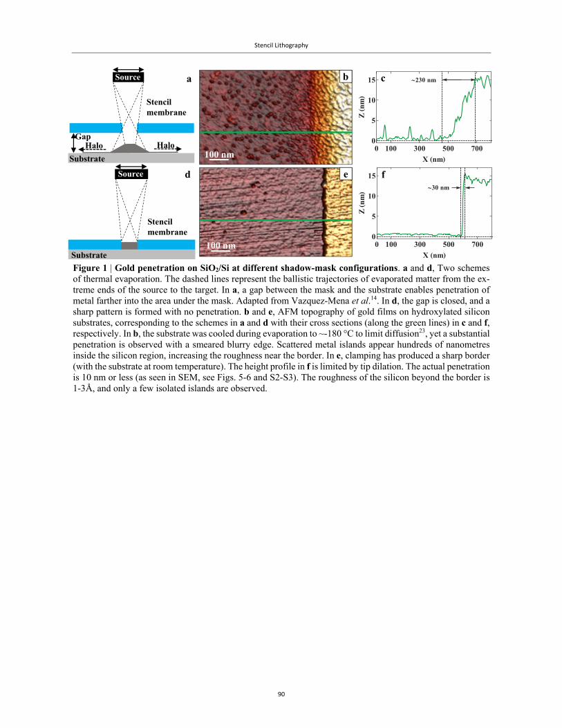
Stencil Lithography
90
Figure 1 | Gold penetration on SiO2/Si at different shadow-mask configurations. a and d, Two schemes of thermal evaporation. The dashed lines represent the ballistic trajectories of evaporated matter from the ex-treme ends of the source to the target. In a, a gap between the mask and the substrate enables penetration of metal farther into the area under the mask. Adapted from Vazquez-Mena et al.14. In d, the gap is closed, and a sharp pattern is formed with no penetration. b and e, AFM topography of gold films on hydroxylated silicon substrates, corresponding to the schemes in a and d with their cross sections (along the green lines) in c and f, respectively. In b, the substrate was cooled during evaporation to ~-180 °C to limit diffusion23, yet a substantial penetration is observed with a smeared blurry edge. Scattered metal islands appear hundreds of nanometres inside the silicon region, increasing the roughness near the border. In e, clamping has produced a sharp border (with the substrate at room temperature). The height profile in f is limited by tip dilation. The actual penetration is 10 nm or less (as seen in SEM, see Figs. 5-6 and S2-S3). The roughness of the silicon beyond the border is 1-3Å, and only a few isolated islands are observed.
100 nm
b c
d
Stencil membrane
Source
Substrate
Stencil membrane
Source
Gap Halo Halo
Substrate
a
f
100 nm
e
0 100 300 500 7000
5
10
15
X nm
Znm
30 nm
0 100 300 500 7000
5
10
15
X nm
Znm
230 nm
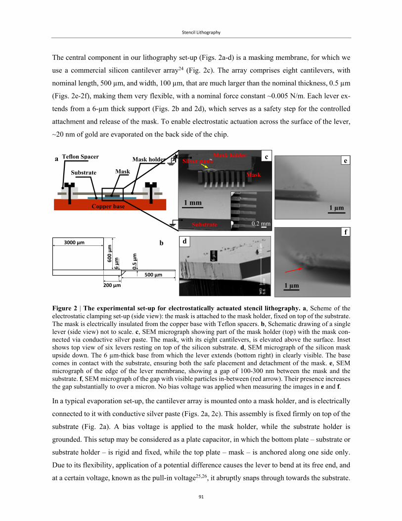
Stencil Lithography
91
The central component in our lithography set-up (Figs. 2a-d) is a masking membrane, for which we
use a commercial silicon cantilever array24 (Fig. 2c). The array comprises eight cantilevers, with
nominal length, 500 µm, and width, 100 µm, that are much larger than the nominal thickness, 0.5 µm
(Figs. 2e-2f), making them very flexible, with a nominal force constant ~0.005 N/m. Each lever ex-
tends from a 6-µm thick support (Figs. 2b and 2d), which serves as a safety step for the controlled
attachment and release of the mask. To enable electrostatic actuation across the surface of the lever,
~20 nm of gold are evaporated on the back side of the chip.
Figure 2 | The experimental set-up for electrostatically actuated stencil lithography. a, Scheme of the electrostatic clamping set-up (side view): the mask is attached to the mask holder, fixed on top of the substrate. The mask is electrically insulated from the copper base with Teflon spacers. b, Schematic drawing of a single lever (side view) not to scale. c, SEM micrograph showing part of the mask holder (top) with the mask con-nected via conductive silver paste. The mask, with its eight cantilevers, is elevated above the surface. Inset shows top view of six levers resting on top of the silicon substrate. d, SEM micrograph of the silicon mask upside down. The 6 µm-thick base from which the lever extends (bottom right) in clearly visible. The base comes in contact with the substrate, ensuring both the safe placement and detachment of the mask. e, SEM micrograph of the edge of the lever membrane, showing a gap of 100-300 nm between the mask and the substrate. f, SEM micrograph of the gap with visible particles in-between (red arrow). Their presence increases the gap substantially to over a micron. No bias voltage was applied when measuring the images in e and f.
In a typical evaporation set-up, the cantilever array is mounted onto a mask holder, and is electrically
connected to it with conductive silver paste (Figs. 2a, 2c). This assembly is fixed firmly on top of the
substrate (Fig. 2a). A bias voltage is applied to the mask holder, while the substrate holder is
grounded. This setup may be considered as a plate capacitor, in which the bottom plate – substrate or
substrate holder – is rigid and fixed, while the top plate – mask – is anchored along one side only.
Due to its flexibility, application of a potential difference causes the lever to bend at its free end, and
at a certain voltage, known as the pull-in voltage25,26, it abruptly snaps through towards the substrate.
c
Mask
Silver paste
0.2 mm
1 mm
Substrate Mask
Teflon Spacer
Copper base
Mask holder
1 µm
e
d
Substrate
Mask holder a
b
1 µm
f
0.5 µm
6 µm
200 µm
500 µm
600
µm
3000 µm
6 µ
m
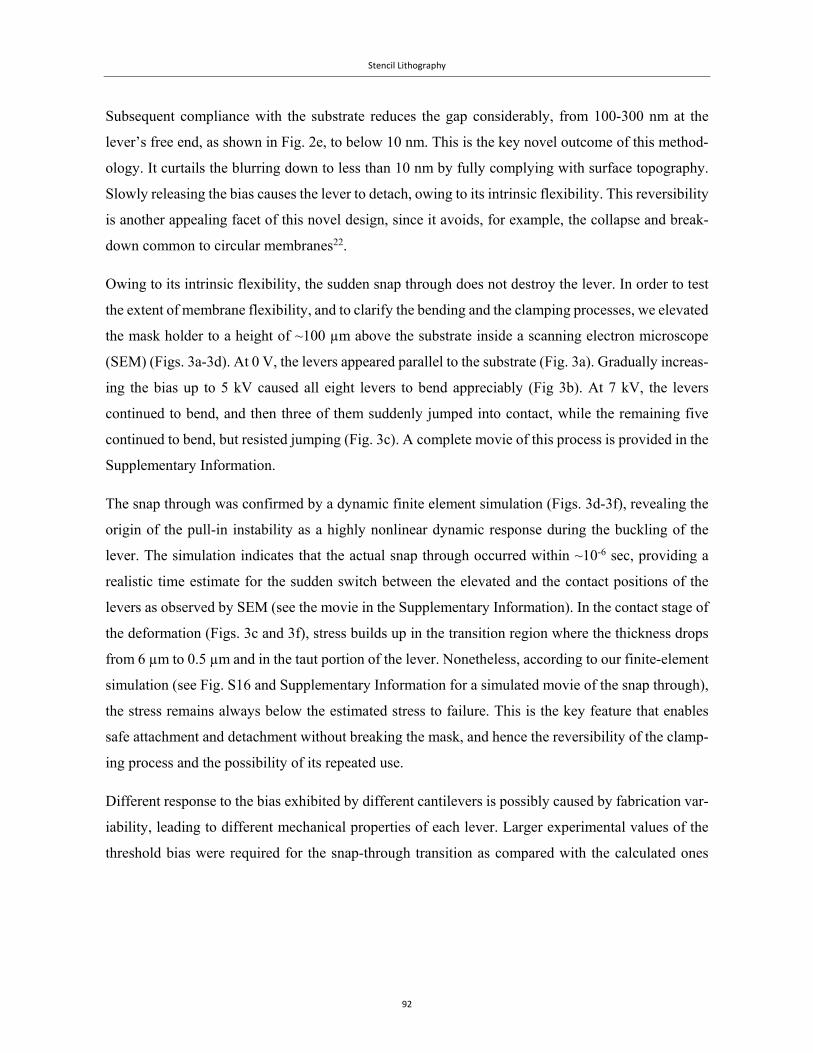
Stencil Lithography
92
Subsequent compliance with the substrate reduces the gap considerably, from 100-300 nm at the
lever’s free end, as shown in Fig. 2e, to below 10 nm. This is the key novel outcome of this method-
ology. It curtails the blurring down to less than 10 nm by fully complying with surface topography.
Slowly releasing the bias causes the lever to detach, owing to its intrinsic flexibility. This reversibility
is another appealing facet of this novel design, since it avoids, for example, the collapse and break-
down common to circular membranes22.
Owing to its intrinsic flexibility, the sudden snap through does not destroy the lever. In order to test
the extent of membrane flexibility, and to clarify the bending and the clamping processes, we elevated
the mask holder to a height of ~100 µm above the substrate inside a scanning electron microscope
(SEM) (Figs. 3a-3d). At 0 V, the levers appeared parallel to the substrate (Fig. 3a). Gradually increas-
ing the bias up to 5 kV caused all eight levers to bend appreciably (Fig 3b). At 7 kV, the levers
continued to bend, and then three of them suddenly jumped into contact, while the remaining five
continued to bend, but resisted jumping (Fig. 3c). A complete movie of this process is provided in the
Supplementary Information.
The snap through was confirmed by a dynamic finite element simulation (Figs. 3d-3f), revealing the
origin of the pull-in instability as a highly nonlinear dynamic response during the buckling of the
lever. The simulation indicates that the actual snap through occurred within ~10-6 sec, providing a
realistic time estimate for the sudden switch between the elevated and the contact positions of the
levers as observed by SEM (see the movie in the Supplementary Information). In the contact stage of
the deformation (Figs. 3c and 3f), stress builds up in the transition region where the thickness drops
from 6 µm to 0.5 µm and in the taut portion of the lever. Nonetheless, according to our finite-element
simulation (see Fig. S16 and Supplementary Information for a simulated movie of the snap through),
the stress remains always below the estimated stress to failure. This is the key feature that enables
safe attachment and detachment without breaking the mask, and hence the reversibility of the clamp-
ing process and the possibility of its repeated use.
Different response to the bias exhibited by different cantilevers is possibly caused by fabrication var-
iability, leading to different mechanical properties of each lever. Larger experimental values of the
threshold bias were required for the snap-through transition as compared with the calculated ones
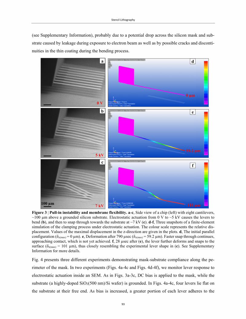
Stencil Lithography
93
(see Supplementary Information), probably due to a potential drop across the silicon mask and sub-
strate caused by leakage during exposure to electron beam as well as by possible cracks and disconti-
nuities in the thin coating during the bending process.
Figure 3 | Pull-in instability and membrane flexibility. a-c, Side view of a chip (left) with eight cantilevers, ~100 µm above a grounded silicon substrate. Electrostatic actuation from 0 V to ~5 kV causes the levers to bend (b), and then to snap through towards the substrate at ~7 kV (c). d-f, Three snapshots of a finite-element simulation of the clamping process under electrostatic actuation. The colour scale represents the relative dis-placement. Values of the maximal displacement in the z-direction are given in the plots. d, The initial parallel configuration (δz(max) = 0 µm). e, Deformation after 790 µsec (δz(max) = 59.2 µm). Faster snap through continues, approaching contact, which is not yet achieved. f, 28 µsec after (e), the lever further deforms and snaps to the surface (δz(max) = 101 µm), thus closely resembling the experimental lever shape in (c). See Supplementary Information for more details.
Fig. 4 presents three different experiments demonstrating mask-substrate compliance along the pe-
rimeter of the mask. In two experiments (Figs. 4a-4c and Figs. 4d-4f), we monitor lever response to
electrostatic actuation inside an SEM. As in Figs. 3a-3c, DC bias is applied to the mask, while the
substrate (a highly-doped SiO2(500 nm)/Si wafer) is grounded. In Figs. 4a-4c, four levers lie flat on
the substrate at their free end. As bias is increased, a greater portion of each lever adheres to the
a
b
c
0 V
5 kV
7 kV100 µm
f
e
d
0 µm
59.2 µm
101 µm
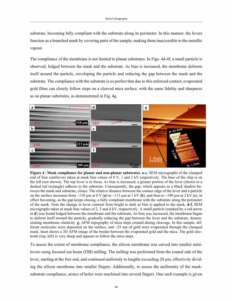
Stencil Lithography
94
substrate, becoming fully compliant with the substrate along its perimeter. In this manner, the levers
function as a branched mask by covering parts of the sample, making them inaccessible to the metallic
vapour.
The compliance of the membrane is not limited to planar substrates. In Figs. 4d-4f, a small particle is
observed, lodged between the mask and the substrate. As bias is increased, the membrane deforms
itself around the particle, enveloping the particle and reducing the gap between the mask and the
substrate. The compliance with the substrate is so perfect that due to this enforced contact, evaporated
gold films can closely follow steps on a cleaved mica surface, with the same fidelity and sharpness
as on planar substrates, as demonstrated in Fig. 4g.
Figure 4 | Mask compliance for planar and non-planar substrates. a-c, SEM micrographs of the clamped end of four cantilevers taken at mask bias values of 0 V, 1 and 2 kV respectively. The base of the chip is on the left (not shown). The top lever is in focus. As bias is increased, a greater portion of the lever (shown in a dashed red rectangle) adheres to the substrate. Consequently, the gap, which appears as a black shadow be-tween the mask and substrate, closes. The relative distance between the contact edge of the lever and a particle on the surface increases from ~110 µm at 0 V (a) to ~113 µm at 1 kV (b), and then to ~190 µm at 2 kV (c), in effect becoming, as the gap keeps closing, a fully compliant membrane with the substrate along the perimeter of the mask. Note the change in lever contrast from bright to dark as bias is applied to the mask. d-f, SEM micrographs taken at mask bias values of 2, 3 and 4 kV, respectively. A small particle (marked by a red arrow in d) was found lodged between the membrane and the substrate. As bias was increased, the membrane began to deform itself around the particle, gradually reducing the gap between the lever and the substrate, demon-strating membrane elasticity. g, AFM topography of mica steps created during cleavage. In this sample, dif-ferent molecules were deposited on the surface, and ~25 nm of gold were evaporated through the clamped mask. Inset shows a 3D AFM image of the border between the evaporated gold and the mica. The gold elec-trode (top, left) is very sharp and appears to follow the mica steps.
To assess the extent of membrane compliance, the silicon membrane was carved into smaller mini-
levers using focused ion beam (FIB) milling. The milling was performed from the coated side of the
lever, starting at the free end, and continued uniformly to lengths exceeding 20 µm, effectively divid-
ing the silicon membrane into smaller fingers. Additionally, to assess the uniformity of the mask-
substrate compliance, arrays of holes were machined into several fingers. One such example is given
a
c
0 V
b
1 kV
2 kV 189 µm
113 µm
110 µm
d
e
f
4 kV
3 kV
2 kV
10 µm
g
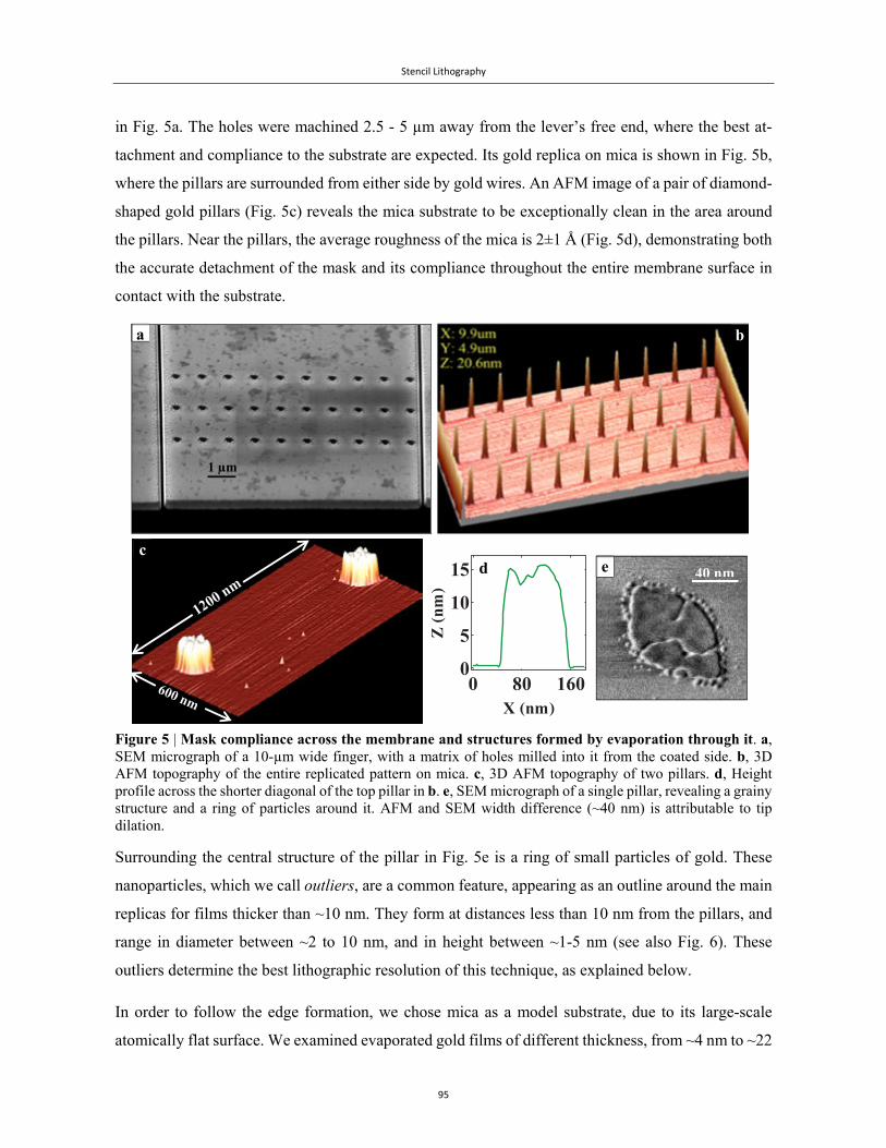
Stencil Lithography
95
in Fig. 5a. The holes were machined 2.5 - 5 µm away from the lever’s free end, where the best at-
tachment and compliance to the substrate are expected. Its gold replica on mica is shown in Fig. 5b,
where the pillars are surrounded from either side by gold wires. An AFM image of a pair of diamond-
shaped gold pillars (Fig. 5c) reveals the mica substrate to be exceptionally clean in the area around
the pillars. Near the pillars, the average roughness of the mica is 2±1 Å (Fig. 5d), demonstrating both
the accurate detachment of the mask and its compliance throughout the entire membrane surface in
contact with the substrate.
Figure 5 | Mask compliance across the membrane and structures formed by evaporation through it. a, SEM micrograph of a 10-µm wide finger, with a matrix of holes milled into it from the coated side. b, 3D AFM topography of the entire replicated pattern on mica. c, 3D AFM topography of two pillars. d, Height profile across the shorter diagonal of the top pillar in b. e, SEM micrograph of a single pillar, revealing a grainy structure and a ring of particles around it. AFM and SEM width difference (~40 nm) is attributable to tip dilation.
Surrounding the central structure of the pillar in Fig. 5e is a ring of small particles of gold. These
nanoparticles, which we call outliers, are a common feature, appearing as an outline around the main
replicas for films thicker than ~10 nm. They form at distances less than 10 nm from the pillars, and
range in diameter between ~2 to 10 nm, and in height between ~1-5 nm (see also Fig. 6). These
outliers determine the best lithographic resolution of this technique, as explained below.
In order to follow the edge formation, we chose mica as a model substrate, due to its large-scale
atomically flat surface. We examined evaporated gold films of different thickness, from ~4 nm to ~22
40 nmd
0 80 1600
5
10
15
X nm
Znm
a b
c e
1 µm
Stencil Lithography
96
nm, formed under similar conditions. Thin films (~4 – 8 nm thick), as those shown in Figs. 6a-6c (see
also Fig. S4), were discontinuous, which is commensurate with the established literature27. The ter-
mination of the layer was very sharp, even though some stray penetration of small isolated grains was
observed. Moreover, the average size of the grains at the frontier is the same as the average grain size
100 - 300 nm inside the film, and generally within the film (see Fig. S4 for details). In thicker layers
(~12 – 22 nm) continuous films were formed27,28, as shown in Figs. 6d-6f. Furthermore, surrounding
the sharp contours of the thicker patterned films are the outliers, as demonstrated in Figs. 5e and 6d-
6f.
The outliers are separate from the main replica and adhere more to the mica substrate than to the main
metallic film, as demonstrated by experiments in which the detachment of the mask from the substrate
had shifted some replicated patterns, probably facilitated by the low adhesion of pure gold to air-
cleaved mica29. In one such case, accidental dislocation of the mask forcibly moved a wire segment
to the right, leaving in place the little gold particles that had surrounded the wire on the left (Fig. 6d).
In another case, a large part of a wire was displaced to the left, exposing the trace of outliers to its
right (Fig. 6f). Several segments of outliers are shown in 3D AFM topography in Fig. 6g.
The width and height of the outliers were measured using SEM and AFM, respectively. In the case
of ~14 nm thick films, as shown, e.g., in Figs. 5e and 6d, the outlier diameter was between 2 to 10
nm (Fig. 6h), and the particles were located a distance of ~10 nm or less from the edge of the replica
(Fig. 6i). In the case of ~22 nm thick films, as shown in Figs. 6e-6f, the outlier diameter increased
only slightly to 2 – 12 nm (Fig. 6j), although additional ~8 nm of gold were evaporated. The height
distribution, 1 – 5 nm (Fig. 6k), is spatially distributed along the perimeter of the replicas, as demon-
strated in Fig. 6g.
Our investigation revealed several observations: (i) when the mask is well clamped, the edge of the
evaporated replica is very sharp and the transition between the underlying substrate and metal regions
is abrupt; (ii) above a certain evaporated thickness threshold (~10–12 nm), gold particles form an
outline around the main replica at a distance of ~10 nm or less from the border (Fig. 6). These outliers
determine the highest resolution achievable with this technique; (iii) the size of the outliers depends
weakly on further deposition beyond this threshold (Fig. 6); (iv) when the gap is not sufficiently small,
even with a collimator (Fig. S1), the metal penetrates into the ballistically-forbidden region charac-
terized by a typical gradient of grain sizes (Figs. S2-S3), from larger grains to nanometre-sized clus-
ters at the outer fringes of the penetration; (v) even in the cases when a highly successful clamping is
Stencil Lithography
97
achieved, i.e., resulting in a sharp border, some small isolated islands are still present in the mica
region beyond the outliers (Figs. 1 and 6).
Figure 6 | The resolution of the technique on mica. a, SEM micrograph of the sharp edge of a gold film (3-4 nm thick). The film appears discontinuous, consisting of small particles, 2 - 9 nm in diameter (see Fig. S2). Stray penetration is observed in the mica region. b, AFM topography of the sample in a. Some stray isolated clusters (1-3 nm high) are observed on the mica. c, Height profile along the green line in b. d, SEM micrograph of a gold wire, ~22 nm thick. Outliers are visible on both sides, beyond which there is no penetration. Scale bar is 50 nm. e, AFM topography of a shifted wire, ~22 nm thick, with outliers exposed on the right. Scale bar is 100 nm. f, SEM micrograph of a gold wire (~14 nm thick), showing outliers on both sides of the wire, and the disconnected outline of the particles on the left of the wire. g, 3D AFM topography of the exposed outliers of patterns as in e, with their vertical dimensions (in nm) in parenthesis. h-i, Normalized histograms of the outlier diameter and distance from the wire (SEM), respectively, for a film thickness, t ~ 14 nm. j-k, Normal-ized histograms of the outlier diameter and height, respectively, for t ~ 22 nm. Each histogram is calculated for a population of 100 particles.
50 nm
a b
0 50 100 150 2000
1
2
3
4
X nm
Znm
23 nm
c
h i
j k
0 2 4 6 8 100
10
20
30
Distance nm
NormalizedCount
t14 nm
2 3 4 50
5
10
Height nm
NormalizedCount
t22 nm
2 4 6 8 10 120.
10
20
30
40
Diameter nm
NormalizedCount
t22 nm
2 4 6 8 100
10
20
30
40
50
Diameter nm
NormalizedCount
t14 nm
100 nm
d g (4)(1.6)
(5)
fe
Stencil Lithography
98
These observations suggest a possible mechanism for the sharp boundary formation in our samples.
When the mask-substrate gap is smaller than ~10 nm, it becomes clogged by incoming vapour at the
initial stages of evaporation. This clogged structure forms the outliers, and their dense spatial arrange-
ment (Fig. 6g) creates a barrier, blocking penetration of subsequent stray atoms and clusters. Their
vertical dimensions (Fig. 6k) indicate the actual size of the mask-substrate gap. The width of the
distribution implies some small variations in the gap along the perimeter of the masking membrane.
The arrested growth of the outliers at an early stage in the formation of the film implies that above a
certain thickness of the film (typically, about 10 nm), additional evaporated gold is mostly deposited
on the main replica, resulting in dense grain growth. This is further supported by the low evaporation
rates in our experiments, which allow a rearrangement of the atoms to form grains on the substrate.27
We interpret the process as follows: trapped under the mask edge, the outliers become disconnected
from the main metallic edifice when the isolated grains begin to coalesce. In this manner, as the film
grows and isolated islands coalesce into grains, the continuous film recedes (due to surface tension),
withdrawing from the border by a few nanometres. The outliers cannot participate in this surface
motion because they are already caught in-between the rim of the mask and the substrate. Such motion
could account for the small space between the sharp border of the replica and the outliers (Fig. 6i).
Surface diffusion has been labelled in the past as the main cause of the penetration14,22. This seems at
odds with our results. If surface diffusion had dominated this process, then a ~10 nm gap would have
allowed smaller clusters or atoms to diffuse thermally beyond this border and well into the region
under the membrane. Sharp boundaries, as those routinely obtained using the technique we described
and demonstrated in this paper, would not have been possible. Moreover, such surface motion would
be strongly affected by changes in substrate temperature. While increasing the temperature of the
substrate (~400 K or more) does extend the penetration17, a substantial decrease in substrate temper-
ature (~80 K) has led to no reduction in the penetration, as shown by Vazquez-Mena et al.14 and
demonstrated in Fig. 1b. This means that penetration can be exacerbated by thermal diffusion, but the
latter is not the main mechanism driving it.
It seems more likely that diffusion processes occur within the metallic replica, as the grains coalesce30,
rather than farther afield. Yet in many cases, even with a highly successful clamping, sparsely scat-
tered and isolated small islands were found on the substrate beyond the sharp edge, as shown, e.g., in
Figs. 1e and 6a-b. Surface diffusion may be partly responsible for their exact position, but their spo-
radic nature, relatively large distance from the main replica and scarcity on the substrate, as well as
their relatively small size, suggest another plausible explanation for their deposition.
Stencil Lithography
99
During thermal evaporation of gold, individual atoms as well as neutral and charged clusters escape
the crucible31-33. Some clusters may also form in the gas phase34. It is possible that the deeper pene-
tration is the result of these hot mobile clusters decaying35 or fragmenting near the substrate (in flight)
as well as through collisions of atoms or clusters with other metal atoms or clusters, the density of
which is not negligible for the typical geometry and conditions we employ31 (see Fig. S1a for details).
In both cases, previously inaccessible incident angles become viable. Such angles – nearly parallel to
the substrate – enable deeper penetration of metal farther under the mask.
The size and shape of these sporadic islands appear to correlate with TEM imaging, capturing the
growth of clusters at various stages of thermal evaporation34,36. Therefore, it seems probable that this
type of stray penetration consists of the remnants of the gold clusters, which had formed at the initial
stages of the evaporation31, and which had penetrated at oblique angles prior to the blocking of the
gap by the outliers.
These considerations may also explain why macroscopic collimation around the mask had reduced
the density of stray atoms and clusters far from the border, but had neither sharpened the shape of the
border nor reduced the penetration in its vicinity (Fig. S1c-d). By forming of a physical barrier, the
collimator did reduce the flux of stray incident penetration, but since decay processes may occur in
close proximity to the surface, a considerable gap (Figs. 2e-2f) between the mask and the substrate
would still permit the penetration of metal clusters at oblique angles. This is consistent with our con-
jecture, that in the case of a smaller gap, at the early stages of the growth of the film, when the gap
was not yet blocked, the disintegrated clusters could penetrate the gap at seemingly inaccessible tra-
jectories. This effect may be more substantial if the clusters are charged. Decaying into smaller
charged clusters, which repel each other, they may break in all directions of flight. As the gold con-
tinues to evaporate, it accumulates on preformed islands, which act both as a physical barrier (self-
shadowing) and a sink (energetic) against further penetration. This suggests that penetration of small
islands occurs at the early stages of evaporation, before the small gap is clogged, in agreement with
our results for thin films (Figs. 6 and S4). These results have been confirmed for additional metals,
such as Ga and Au-Ge (see Fig. S5).
In conclusion, we report a versatile technique for chemical-free stencil lithography with nanometre
precision applied successfully to various substrates, metals and surface geometries. The technique
has already found numerous applications in molecular electronics20, and may prove useful in a variety
Stencil Lithography
100
of applications, including lithography, catalysis37, nano-electronics, NEMs and MEMs devices. Fur-
thermore, we provide a plausible explanation to the long-standing question about the mechanism of
penetration under the mask that has limited so far the resolution and sharpness of replica formation.
Methods
Silicon cantilever arrays (CLA-500-005-08, Concentris Inc.) are fabricated from p-doped silicon (4×10¹⁶
atom/cm3), and were developed originally for high-sensitivity adsorption experiments. Samples for evapora-
tion were hydroxylated silicon wafers, bare mica or mica with absorbed molecules. In all cases, the sample-
mask assembly was mounted on top of a cold finger inside a thermal evaporator (modified Edwards E306),
directly above the centre of the crucible. To avoid mask damage by transient voltages, a high-voltage DC
power supply (homemade) was first turned on, set to 0 V, and only then connected through an electrical feed-
through to the mask holder. When pressure had reached ≈2x10⁻⁶ torr, a cold trap was cooled with liquid nitro-
gen down to ≈-190 °C (measured by a type T thermocouple connected to the copper base plate). At this point,
electrostatic actuation of the levers would commence. In the case of a bare substrate, the bias was gradually
raised (~1V / 1 sec) to 100-200 V. The evaporation rate was monitored by a thickness monitor (FTM4, BOC
Edwards), and the sample shutter was opened when the rate reached ≈1 Å/min. Typically, slow evaporation
would continue for the first 2-4 nm. The evaporation rate was gradually increased by a factor of 2-4 until the
end of the coating. A gold layer was evaporated typically within 60-90 min. At the end of the evaporation,
mask bias was gradually decreased (~1V / 1 sec) back to 0 V. The procedure was modified when the substrate
was covered with molecules. To reduce radiative heating of the target, the sample holder was cooled by a
cooling agent flow. Prior to cooling, bias voltage was gradually applied to the mask up to 100-200 V. As the
cooling commenced, the substrate’s temperature dropped within 30 s to ≈-11 °C. Then gradually, the bias was
further raised to ~300-400 V until the temperature reached -25 °C. As soon as the temperature stabilized, slow
evaporation began at ≈1 Å/min. At the end of the process, the substrate was gradually heated to 14 °C, at which
point the mask bias was decreased back to 0 V. AFM imaging was done with SmartSPM™ 1000 (AIST-NT).
Samples were measured using soft cantilevers (OMCL-RC800PSA, Olympus Optical Co., Ltd) of nominal
force constant 0.3 N/m. AFM images were analysed using a Nanotec Electronica S.L (Madrid) WSxM imaging
software38. SEM imaging was done with Quanta 200 and Magellan 400L (both - FEI Company, USA). Elec-
trostatic clamping was monitored by imaging with secondary electrons in Quanta operated at 5-20 kV. The
finest structural details of the tested samples were studied with Magellan operated at 1-2 kV with and without
application of 500 V cathode bias. FIB milling was performed using Zeiss Crossbeam1540XB equipped with
Raith Elphy Plus lithography system. Patterns were typically written with an ion current of 50 pA. Basic con-
cepts of the finite element modelling are based on Livshits and Saltoun39 and Livshits, Yaniv and Karpel40.
Stencil Lithography
101
References
1 Holland, L. Vacuum Deposition of Thin Films. (Chapman and Hall Ltd. London, 1966). 2 Jiang, L., Dong, H. L. & Hu, W. P. Organic single crystal field‐effect transistors: advances and perspectives. J
Mater Chem 20, 4994‐5007 (2010). 3 Welte, L., Calzolari, A., Di Felice, R., Zamora, F. & Gomez‐Herrero, J. Highly conductive self‐assembled nano‐
ribbons of coordination polymers. Nat Nanotechnol 5, 110‐115 (2010). 4 de Pablo, P. J. et al. Mechanical and electrical properties of nanosized contacts on single‐walled carbon nano‐
tubes. Adv Mater 12, 573‐576 (2000). 5 de Pablo, P. J. et al. Absence of dc‐conductivity in lambda‐DNA. Phys Rev Lett 85, 4992‐4995 (2000). 6 Sidler, K. et al. Resistivity measurements of gold wires fabricated by stencil lithography on flexible polymer
substrates. Microelectronic Engineering 85, 1108‐1111 (2008). 7 Villanueva, L. G. et al. All‐stencil transistor fabrication on 3D silicon substrates. Journal of Micromechanics
and Microengineering 22, 095022 (2012). 8 Vazquez‐Mena, O., Sannomiya, T., Villanueva, L. G., Voros, J. & Brugger, J. Metallic Nanodot Arrays by Stencil
Lithography for Plasmonic Biosensing Applications. Acs Nano 5, 844‐853 (2011). 9 Deshmukh, M. M., Ralph, D. C., Thomas, M. & Silcox, J. Nanofabrication using a stencil mask. Appl Phys Lett
75, 1631‐1633 (1999). 10 Vazquez‐Mena, O. et al. High‐Resolution Resistless Nanopatterning on Polymer and Flexible Substrates for
Plasmonic Biosensing Using Stencil Masks. Acs Nano 6, 5474‐5481 (2012). 11 Egger, S. et al. Dynamic shadow mask technique: A universal tool for nanoscience. Nano Letters 5, 15‐20
(2005). 12 Villanueva, G. et al. Etching of sub‐micrometer structures through Stencil. Microelectron Eng 85, 1010‐1014
(2008). 13 Villanueva, L. G. et al. Localized Ion Implantation Through Micro/Nanostencil Masks. Ieee T Nanotechnol 10,
940‐946 (2011). 14 Vazquez‐Mena, O. et al. Analysis of the blurring in stencil lithography. Nanotechnology 20, 415303 (2009). 15 Racz, Z. & Seabaugh, A. Characterization and control of unconfined lateral diffusion under stencil masks. J Vac
Sci Technol B 25, 857‐861 (2007). 16 Doust, T., Metcalfe, F. L. & Venables, J. A. Biased Secondary‐Electron Imaging Studies of Ag/Si(111). Ultrami‐
croscopy 31, 116‐123 (1989). 17 Levenson, L. L., Swartzlander, A. B., Yahashi, A., Usui, H. & Yamada, I. Aluminum Surface Mobility on Silicon‐
Nitride and on Several Silicon‐Oxides. J Vac Sci Technol A 8, 1447‐1452 (1990). 18 Podzorov, V., Sysoev, S. E., Loginova, E., Pudalov, V. M. & Gershenson, M. E. Single‐crystal organic field effect
transistors with the hole mobility similar to 8 cm(2)/V s. Appl Phys Lett 83, 3504‐3506 (2003). 19 Chepelianskii, A. D. et al. Long range electronic transport in DNA molecules deposited across a disconnected
array of metallic nanoparticles. Cr Phys 13, 967‐992 (2012). 20 Livshits, G. I. et al. Long‐range charge transport in single G‐quadruplex DNA molecules. Nat Nanotechnol In
Press (2014). 21 Sidler, K., Villanueva, L. G., Vazquez‐Mena, O., Savu, V. & Brugger, J. Compliant membranes improve resolu‐
tion in full‐wafer micro/nanostencil lithography. Nanoscale 4, 773‐778 (2012). 22 Couderc, S., Blech, V. & Kim, B. New Surface Treatment and Microscale/Nanoscale Surface Patterning Using
Electrostatically Clamped Stencil Mask. Japanese Journal of Applied Physics 48, 095007 (2009). 23 Buchholz, S., Fuchs, H. & Rabe, J. P. Surface‐Structure of Thin Metallic‐Films on Mica as Seen by Scanning Tun‐
neling Microscopy, Scanning Electron‐Microscopy, and Low‐Energy Electron‐Diffraction. J Vac Sci Technol B 9, 857‐861 (1991).
24 Fritz, J. Cantilever biosensors. Analyst 133, 855‐863 (2008). 25 Senturia, S. D. Microsystem Design. (Kluwer Academic Pulishers, 2002). 26 Rebeiz, G. M. RF MEMS: Theory, Design and Technology. (John Wiley & Sons, 2003). 27 Bahamondes, S., Donoso, S., Henriquez, R. & Flores, M. Morphological and electrical study of gold ultrathin
films on mica. Thin Solid Films 548, 646‐649 (2013). 28 Allpress, J. G. & Sanders, J. V. Structure and Orientation of Crystals in Deposits of Metals on Mica. Surf Sci 7,
1‐& (1967). 29 Higginbotham, I. G., Williams, R. H. & Mcevoy, A. J. Metal‐Non‐Metal Interfaces ‐ Adhesion of Gold on Mica. J
Phys D Appl Phys 8, 1033‐1043 (1975).
Stencil Lithography
102
30 Higo, M., Fujita, K., Tanaka, Y., Mitsushio, M. & Yoshidome, T. Surface morphology of metal films deposited on mica at various temperatures observed by atomic force microscopy. Appl Surf Sci 252, 5083‐5099 (2006).
31 Hwang, N. M. & Lee, D. K. Charged nanoparticles in thin film and nanostructure growth by chemical vapour deposition. J Phys D Appl Phys 43 (2010).
32 Peineke, C., Attoui, M. B. & Schmidt‐Ott, A. Using a glowing wire generator for production of charged, uni‐formly sized nanoparticles at high concentrations. J Aerosol Sci 37, 1651‐1661 (2006).
33 Peineke, C. & Schmidt‐Ott, A. Explanation of charged nanoparticle production from hot surfaces. J Aerosol Sci 39, 244‐252 (2008).
34 Barnes, M. C., Kim, D. Y., Ahn, H. S., Lee, C. O. & Hwang, N. M. Deposition mechanism of gold by thermal evaporation: approach by charged cluster model. J Cryst Growth 213, 83‐92 (2000).
35 Rabinovitch, R., Hansen, K. & Kresin, V. V. Slow Electron Attachment as a Probe of Cluster Evaporation Pro‐cesses. J Phys Chem A 115, 6961‐6972 (2011).
36 Barnes, M. C., Jeon, I. D., Kim, D. Y. & Hwang, N. M. Generation of charged clusters during thermal evapora‐tion of gold. J Cryst Growth 242, 455‐462 (2002).
37 Choi, J., Koh, K. & Kim, J. Scalable and number‐controlled synthesis of carbon nanotubes by nanostencil li‐thography. Nanoscale Research Letters 8, 281 (2013).
38 Horcas, I. et al. WSXM: A software for scanning probe microscopy and a tool for nanotechnology. Rev Sci In‐strum 78 (2007).
39 Livshits, D. S. & Saltoun, D. in MSC/NASTRAN World User’s Conference Vol. 36 (MacNeal‐Schwendler Corpo‐ration, Florida, 1995).
40 Livshits, D. S., Yaniv, S. & Karpel, M. in 37th Structures, Structural Dynamics and Materials Conference Vol. 37 230‐236 (AMERICAN INSTITUTE OF AERONAUTICS AND ASTRONAUTICS, Salt Lake City, 1996).
Acknowledgements We thank Tal Dagan, Dmitry Evplov, Jacob Livshits, Evgenia Blayvas, Avi Ben-Hur, Alexander Puzenko and Igor Brodsky for technical support and fruitful discussions. This work was supported by the European Commission through grants ‘DNA-based Nanowires’ (IST–2001-38951), ‘DNA-based Nanodevices’ (FP6-029192) and FP7-ERC 226628; the ESF COST MP0802; the Israel Science Foundation (grant no. 1145/10); the BSF grant 2006422 and The Minerva Centre for Bio-Hybrid complex systems of the Hebrew University of Jerusalem.
Author Contributions G.I.L. and D.P. conceived and designed the reported research. G.I.L. prepared the samples and per-formed the AFM measurements. E.M.M. constructed the mask holder and provided expert technical support. I.P. and R.Z. performed SEM measurements assisted by G.I.L. D.S.L. performed finite ele-ment calculations. P.K.K. and L.G. designed and performed FIB milling of the mask. G.I.L., E.M.M., I.P., D.R., S.J.W., L.G. and D.P. analysed the data. G.I.L. and E.M.M. proposed the boundary for-mation and stray penetration mechanisms. All authors discussed the results. G.I.L., E.M.M., I.P., S.J.W., L.G. and D.P. wrote the manuscript, assisted by all authors. Author Information The authors declare no competing financial interests. Correspondence and re-quests for materials should be addressed to L.G. ([email protected]) and D.P. ([email protected]).
103
4.2 Supplementaryinformation
Supplementary Information for
Chemical-free lithography with nanometre-precision via reversible
electrostatic clamping
Below we provide additional examples of samples, control measurements, experimental schemes and
numerical simulations for the behaviour of our setup, as explained in the manuscript. Specifically,
Section 1 is devoted to additional experimental data, which complement the main text. Fig. S1 shows
the scheme of the evaporator (Fig. S1a) and the results of evaporation when a collimator was
positioned around the mask (Fig. S1b-d). Varying degress of penetration of gold on mica are explored
in Fig. S2, while the penetration of gold on hydroxylated silicon along the perimeter of the mask is
shown in Fig. S3. Additional information on thin films is provided in Fig. S4. Additional examples
of accurate metal deposition with other metals are given in Fig. S5.
In Section 2, we discuss the highly nonlinear dynamic contact simulation using the MSC.Nastran
code, which was employed to account for the electrostatic force between the lever and the substrate.
Figs. S6-S7 show the dimensions of the physical and simulated model, and the applied load diagram,
respectively. Fig. S8 shows the translation of the lever as a function of time, as bias voltage is in-
creased to the mask. Special attention is given to the essential snap through process (Fig. S8c), with
a series of snapshots of the deflection of the lever towards the substrate and in contact with it (Figs.
S9-S15). A plot of the maximum stress of the lever at the maximal deformation is shown in Fig. S16.
Additional references are provided in Section 3.
Additional supplementary materials
Two movies are provided separately as supplementary materials. The first movie, electro-
static_clamping.mov, was referred to in Figs. 3a-3c in the manuscript. It is a compilation of 168
consecutive SEM micrographs monitoring the electrostatic actuation of all eight levers, taken in the
QUANTA SEM system. The second movie, fem_simulation.mov, is a finite element simulation (see
section 2) of the snap through of a single cantilever, composed of 75 frames.
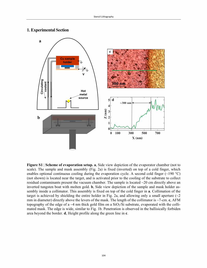
Stencil Lithography
104
1. Experimental Section
Figure S1 | Scheme of evaporation setup. a, Side view depiction of the evaporator chamber (not to scale). The sample and mask assembly (Fig. 2a) is fixed (inverted) on top of a cold finger, which enables optional continuous cooling during the evaporation cycle. A second cold finger (~190 °C) (not shown) is located near the target, and is activated prior to the cooling of the substrate to collect residual contaminants present the vacuum chamber. The sample is located ~20 cm directly above an inverted tungsten boat with molten gold. b, Side view depiction of the sample and mask holder as-sembly inside a collimator. This assembly is fixed on top of the cold finger in a. Collimation of the target is achieved by shielding the entire holder in Fig. 2a, and allowing only a small aperture (~2 mm in diameter) directly above the levers of the mask. The length of the collimator is ~7-cm. c, AFM topography of the edge of a ~4 nm thick gold film on a SiO2/Si substrate, evaporated with the colli-mated mask. The edge is wide, similar to Fig. 1b. Penetration is observed in the ballisically forbiden area beyond the border. d, Height profile along the green line in c.
a
b
Hot metal
source
Cu sample holder
V
Cir
cu
lati
ng
co
ola
nt
d
300 nm
c
0 100 300 500 700
0
1
2
3
4
5
X nm
Znm
300 nm
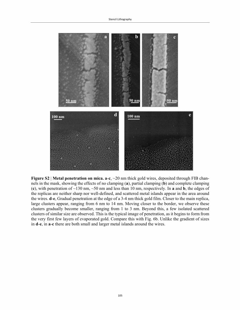
Stencil Lithography
105
Figure S2 | Metal penetration on mica. a-c, ~20 nm thick gold wires, deposited through FIB chan-nels in the mask, showing the effects of no clamping (a), partial clamping (b) and complete clamping (c), with penetration of ~130 nm, ~50 nm and less than 10 nm, respectively. In a and b, the edges of the replicas are neither sharp nor well-defined, and scattered metal islands appear in the area around the wires. d-e, Gradual penetration at the edge of a 3-4 nm thick gold film. Closer to the main replica, large clusters appear, ranging from 6 nm to 14 nm. Moving closer to the border, we observe these clusters gradually become smaller, ranging from 1 to 3 nm. Beyond this, a few isolated scattered clusters of similar size are observed. This is the typical image of penetration, as it begins to form from the very first few layers of evaporated gold. Compare this with Fig. 6b. Unlike the gradient of sizes in d-e, in a-c there are both small and larger metal islands around the wires.
100 nm 100 nmd e
50 nm
a b
50 nm 50 nm
c
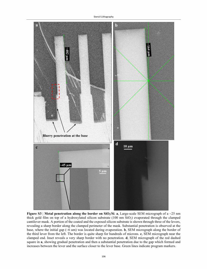
Stencil Lithography
106
Figure S3 | Metal penetration along the border on SiO2/Si. a, Large-scale SEM micrograph of a ~25 nm thick gold film on top of a hydroxylated silicon substrate (100 nm SiO2) evaporated through the clamped cantilever mask. A portion of the coated and the exposed silicon substrate is shown through three of the levers, revealing a sharp border along the clamped perimeter of the mask. Substantial penetration is observed at the base, where the initial gap (~6 um) was located during evaporation. b, SEM micrograph along the border of the third lever from the left. The border is quite sharp for hundreds of microns. c, SEM micrograph near the clamped end. Inset reveals a very sharp border with no penetration. d, SEM micrograph of the red dashed square in a, showing gradual penetration and then a substantial penetration due to the gap which formed and increases between the lever and the surface closer to the lever base. Green lines indicate program markers.
c
~45 µm
a b
5 µm
~482 µm
Blurry penetration at the base
10 µmd
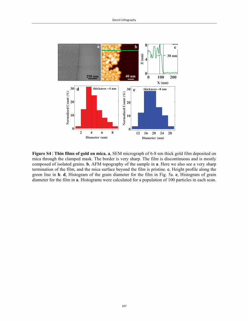
Stencil Lithography
107
Figure S4 | Thin films of gold on mica. a, SEM micrograph of 6-8 nm thick gold film deposited on mica through the clamped mask. The border is very sharp. The film is discontinuous and is mostly composed of isolated grains. b, AFM topography of the sample in a. Here we also see a very sharp termination of the film, and the mica surface beyond the film is pristine. c, Height profile along the green line in b. d, Histogram of the grain diameter for the film in Fig. 5a. e, Histogram of grain diameter for the film in a. Histograms were calculated for a population of 100 particles in each scan.
250 nm 40 nm
a b
0 100 2000
4
8
X nm
Znm
30 nm
c
2 4 6 80
10
20
30
Diameter nm
NormalizedCount
thickness4 nmd
12 16 20 24 280
10
20
30
Diameter nm
NormalizedCount
thickness8 nme
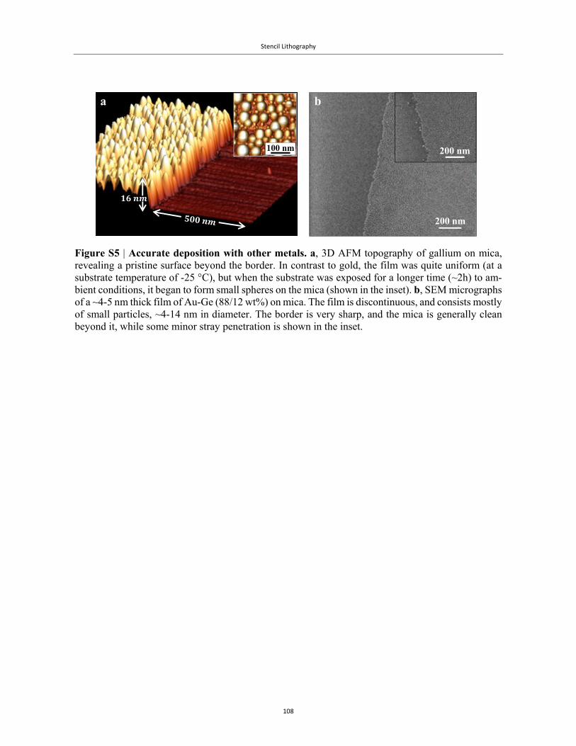
Stencil Lithography
108
Figure S5 | Accurate deposition with other metals. a, 3D AFM topography of gallium on mica, revealing a pristine surface beyond the border. In contrast to gold, the film was quite uniform (at a substrate temperature of -25 °C), but when the substrate was exposed for a longer time (~2h) to am-bient conditions, it began to form small spheres on the mica (shown in the inset). b, SEM micrographs of a ~4-5 nm thick film of Au-Ge (88/12 wt%) on mica. The film is discontinuous, and consists mostly of small particles, ~4-14 nm in diameter. The border is very sharp, and the mica is generally clean beyond it, while some minor stray penetration is shown in the inset.
a
100 nm
200 nm
200 nm
b
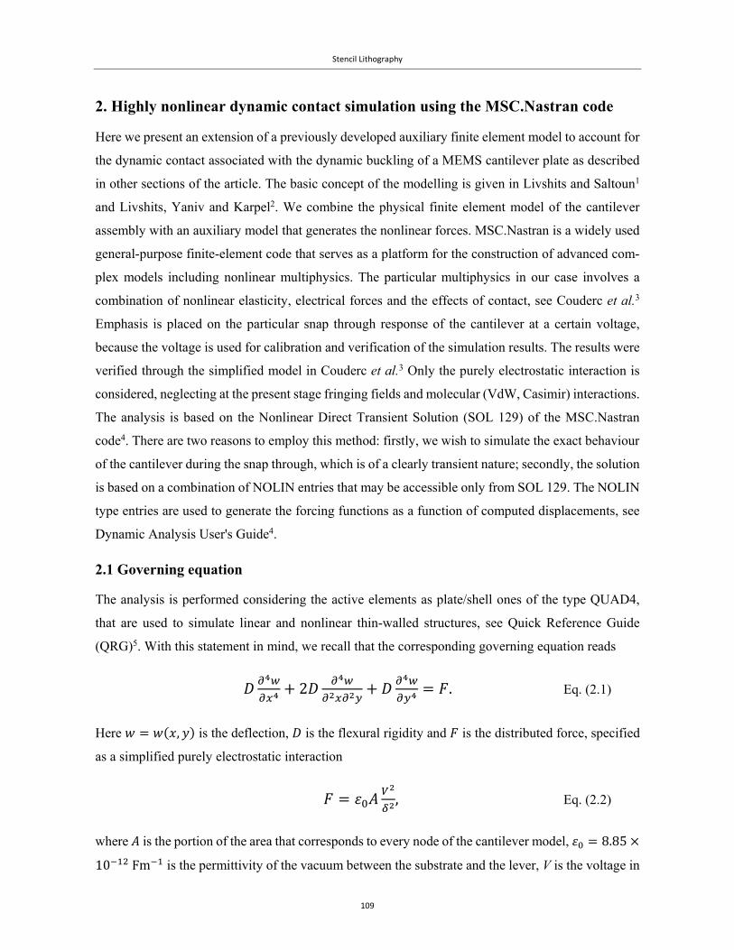
Stencil Lithography
109
2. Highly nonlinear dynamic contact simulation using the MSC.Nastran code
Here we present an extension of a previously developed auxiliary finite element model to account for
the dynamic contact associated with the dynamic buckling of a MEMS cantilever plate as described
in other sections of the article. The basic concept of the modelling is given in Livshits and Saltoun1
and Livshits, Yaniv and Karpel2. We combine the physical finite element model of the cantilever
assembly with an auxiliary model that generates the nonlinear forces. MSC.Nastran is a widely used
general-purpose finite-element code that serves as a platform for the construction of advanced com-
plex models including nonlinear multiphysics. The particular multiphysics in our case involves a
combination of nonlinear elasticity, electrical forces and the effects of contact, see Couderc et al.3
Emphasis is placed on the particular snap through response of the cantilever at a certain voltage,
because the voltage is used for calibration and verification of the simulation results. The results were
verified through the simplified model in Couderc et al.3 Only the purely electrostatic interaction is
considered, neglecting at the present stage fringing fields and molecular (VdW, Casimir) interactions.
The analysis is based on the Nonlinear Direct Transient Solution (SOL 129) of the MSC.Nastran
code4. There are two reasons to employ this method: firstly, we wish to simulate the exact behaviour
of the cantilever during the snap through, which is of a clearly transient nature; secondly, the solution
is based on a combination of NOLIN entries that may be accessible only from SOL 129. The NOLIN
type entries are used to generate the forcing functions as a function of computed displacements, see
Dynamic Analysis User's Guide4.
2.1 Governing equation
The analysis is performed considering the active elements as plate/shell ones of the type QUAD4,
that are used to simulate linear and nonlinear thin-walled structures, see Quick Reference Guide
(QRG)5. With this statement in mind, we recall that the corresponding governing equation reads
2 . Eq. (2.1)
Here , is the deflection, is the flexural rigidity and is the distributed force, specified
as a simplified purely electrostatic interaction
, Eq. (2.2)
where is the portion of the area that corresponds to every node of the cantilever model, 8.85
10 Fm is the permittivity of the vacuum between the substrate and the lever, V is the voltage in
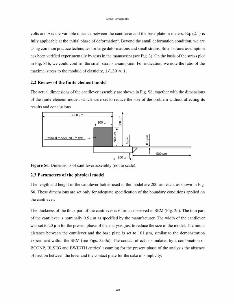
Stencil Lithography
110
volts and δ is the variable distance between the cantilever and the base plate in meters. Eq. (2.1) is
fully applicable at the initial phase of deformation6. Beyond the small deformation condition, we are
using common practice techniques for large deformations and small strains. Small strains assumption
has been verified experimentally by tests in the manuscript (see Fig. 3). On the basis of the stress plot
in Fig. S16, we could confirm the small strains assumption. For indication, we note the ratio of the
maximal stress to the module of elasticity, 1 130⁄ ≪ 1.
2.2 Review of the finite element model
The actual dimensions of the cantilever assembly are shown in Fig. S6, together with the dimensions
of the finite element model, which were set to reduce the size of the problem without affecting its
results and conclusions.
Figure S6. Dimensions of cantilever assembly (not to scale).
2.3 Parameters of the physical model
The length and height of the cantilever holder used in the model are 200 µm each, as shown in Fig.
S6. These dimensions are set only for adequate specification of the boundary conditions applied on
the cantilever.
The thickness of the thick part of the cantilever is 6 µm as observed in SEM (Fig. 2d). The thin part
of the cantilever is nominally 0.5 µm as specified by the manufacturer. The width of the cantilever
was set to 20 µm for the present phase of the analysis, just to reduce the size of the model. The initial
distance between the cantilever and the base plate is set to 101 µm, similar to the demonstration
experiment within the SEM (see Figs. 3a-3c). The contact effect is simulated by a combination of
BCONP, BLSEG and BWIDTH entries5 assuming for the present phase of the analysis the absence
of friction between the lever and the contact plate for the sake of simplicity.
200 µm
0.5 µm
6 µm
200 µm
200 µm500 µm
600 µm
3000 µm
Physical model, 20 µm thk
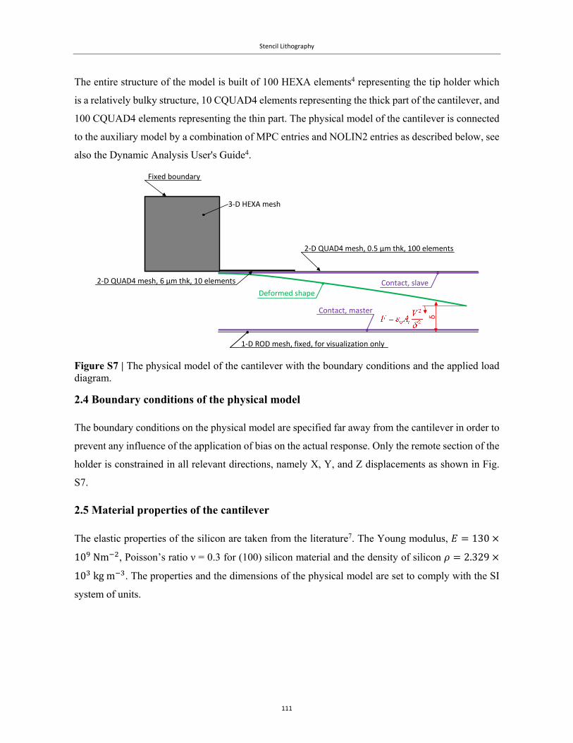
Stencil Lithography
111
The entire structure of the model is built of 100 HEXA elements4 representing the tip holder which
is a relatively bulky structure, 10 CQUAD4 elements representing the thick part of the cantilever, and
100 CQUAD4 elements representing the thin part. The physical model of the cantilever is connected
to the auxiliary model by a combination of MPC entries and NOLIN2 entries as described below, see
also the Dynamic Analysis User's Guide4.
Figure S7 | The physical model of the cantilever with the boundary conditions and the applied load diagram.
2.4 Boundary conditions of the physical model
The boundary conditions on the physical model are specified far away from the cantilever in order to
prevent any influence of the application of bias on the actual response. Only the remote section of the
holder is constrained in all relevant directions, namely X, Y, and Z displacements as shown in Fig.
S7.
2.5 Material properties of the cantilever
The elastic properties of the silicon are taken from the literature7. The Young modulus, 130
10 Nm , Poisson’s ratio ν = 0.3 for (100) silicon material and the density of silicon 2.329
10 kgm . The properties and the dimensions of the physical model are set to comply with the SI
system of units.
Fixed boundary
3‐D HEXA mesh
2‐D QUAD4 mesh, 6 µm thk, 10 elements
2‐D QUAD4 mesh, 0.5 µm thk, 100 elements
1‐D ROD mesh, fixed, for visualization only
Contact, master
Contact, slave
δ
Deformed shape
Stencil Lithography
112
2.6 Auxiliary model description
The auxiliary model consists of 446 CROD elements5 whose stiffness parameters are set to 1.0 as
described in Livshits and Saltoun1. The purpose of the auxiliary model is to simulate the loads applied
to the physical model as a function of the running solution variables.
Presently, we consider only effects induced by the electrostatic interaction, which takes the form of
Eq. (2.2). The CROD elements of the auxiliary are divided into two groups: (1) direct load application
group, and (2) a load-dependent group used to generate the load as a function of the current defor-
mation of each grid in the physical model. The latter group is used to convert the displacement in the
physical model into the force applied on each node of the physical model. In this manner, we identify
the deformation mechanism followed by subsequent snap through at a certain voltage. The total num-
ber of CROD elements in each group corresponds to the active node number of the physical model.
The boundary conditions of the CROD elements are fully clamped in the base nodes, and allow dis-
placement at the other node of each element. In Fig. S7, a schematic depiction of the relative dis-
placement of the lever is given. In each iteration, it is computed through the MPC entry, which results
from the combined displacement of the physical model and the location of the base.
2.7 The external load application procedure
We distinguish between two regimes, characterized by two very different time scales. In the slow
regime, electrostatic actuation causes the lever to bend until the moment of snap through is reached.
In the fast regime, snap through occurs. In order to capture both regimes, it is necessary to quickly
ramp the bias to ~750 V and to show the snap through that occurs in a very short time, ~10-6 sec. The
voltage is applied on the auxiliary model by a combination of CROD elements and a NOLIN1 entry.
For clarity of the model description: all terms related to specific NASTRAN notations are adequately
described in QRG5, which is accessible for any reader in the scientific community.
2.8 Finite element analysis of the dynamic response
The dynamic response of the cantilever is computed using the Nonlinear Direct Transient Algorithm
of MSC.Nastran, namely SOL 1294. The solution was obtained using 4100 time steps of 0.2 µsec.
The time step was eventually reduced at some occasions by two orders of magnitude to 2 nsec, re-
quired to catch the buckling type response of the cantilever. The dynamic response of the cantilever
clearly shows a sudden deformation at the pull-in voltage, whereas under a lower voltage it demon-
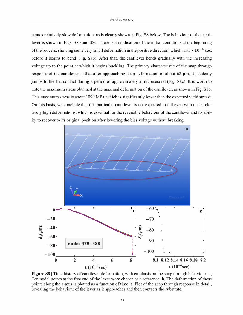
Stencil Lithography
113
strates relatively slow deformation, as is clearly shown in Fig. S8 below. The behaviour of the canti-
lever is shown in Figs. S8b and S8c. There is an indication of the initial conditions at the beginning
of the process, showing some very small deformation in the positive direction, which lasts~10 sec,
before it begins to bend (Fig. S8b). After that, the cantilever bends gradually with the increasing
voltage up to the point at which it begins buckling. The primary characteristic of the snap through
response of the cantilever is that after approaching a tip deformation of about 62 µm, it suddenly
jumps to the flat contact during a period of approximately a microsecond (Fig. S8c). It is worth to
note the maximum stress obtained at the maximal deformation of the cantilever, as shown in Fig. S16.
This maximum stress is about 1090 MPa, which is significantly lower than the expected yield stress8.
On this basis, we conclude that this particular cantilever is not expected to fail even with these rela-
tively high deformations, which is essential for the reversible behaviour of the cantilever and its abil-
ity to recover to its original position after lowering the bias voltage without breaking.
Figure S8 | Time history of cantilever deformation, with emphasis on the snap through behaviour. a, Ten nodal points at the free end of the lever were chosen as a reference. b, The deformation of these points along the z-axis is plotted as a function of time. c, Plot of the snap through response in detail, revealing the behaviour of the lever as it approaches and then contacts the substrate.
0 2 4 6 8
0
20
40
60
80
100
t 104sec
Δ zΜm
nodes 479488
8.1 8.12 8.14 8.16 8.18 8.2
60
70
80
90
100
t 104sec
Δ zΜm
cb
a
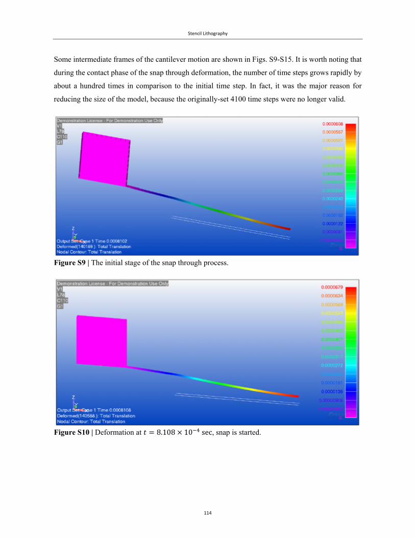
Stencil Lithography
114
Some intermediate frames of the cantilever motion are shown in Figs. S9-S15. It is worth noting that
during the contact phase of the snap through deformation, the number of time steps grows rapidly by
about a hundred times in comparison to the initial time step. In fact, it was the major reason for
reducing the size of the model, because the originally-set 4100 time steps were no longer valid.
Figure S9 | The initial stage of the snap through process.
Figure S10 | Deformation at 8.108 10 sec, snap is started.
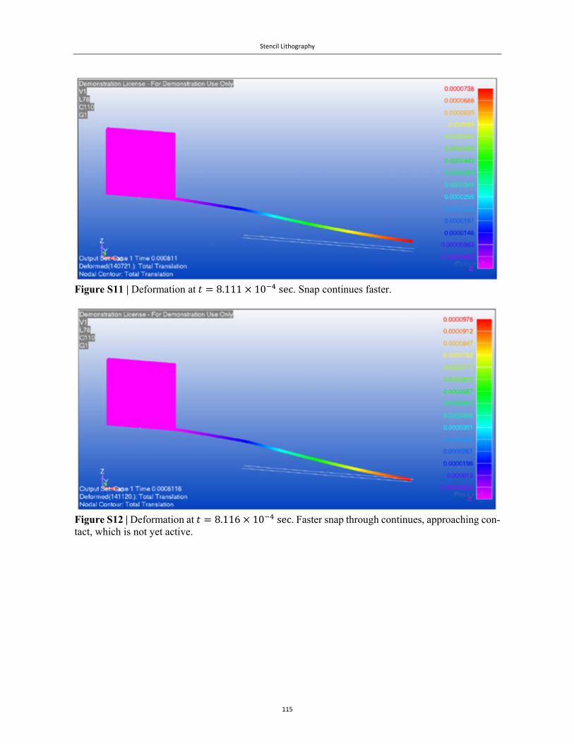
Stencil Lithography
115
Figure S11 | Deformation at 8.111 10 sec. Snap continues faster.
Figure S12 | Deformation at 8.116 10 sec. Faster snap through continues, approaching con-tact, which is not yet active.
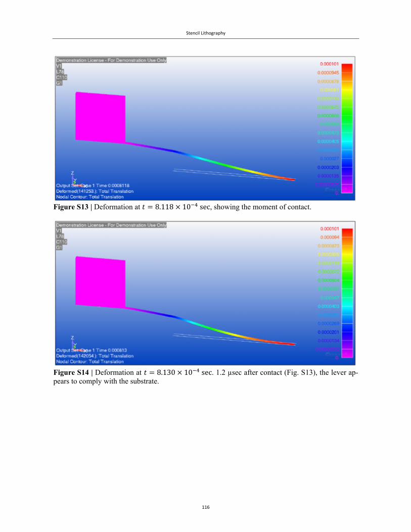
Stencil Lithography
116
Figure S13 | Deformation at 8.118 10 sec, showing the moment of contact.
Figure S14 | Deformation at 8.130 10 sec. 1.2 µsec after contact (Fig. S13), the lever ap-pears to comply with the substrate.
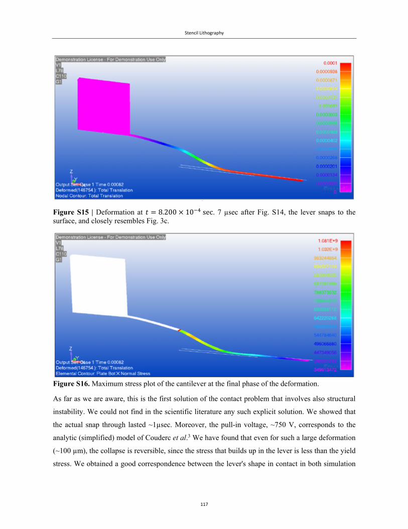
Stencil Lithography
117
Figure S15 | Deformation at 8.200 10 sec. 7 µsec after Fig. S14, the lever snaps to the surface, and closely resembles Fig. 3c.
Figure S16. Maximum stress plot of the cantilever at the final phase of the deformation.
As far as we are aware, this is the first solution of the contact problem that involves also structural
instability. We could not find in the scientific literature any such explicit solution. We showed that
the actual snap through lasted ~1µsec. Moreover, the pull-in voltage, ~750 V, corresponds to the
analytic (simplified) model of Couderc et al.3 We have found that even for such a large deformation
(~100 µm), the collapse is reversible, since the stress that builds up in the lever is less than the yield
stress. We obtained a good correspondence between the lever's shape in contact in both simulation

Stencil Lithography
118
and experiment. Most importantly, our methodology allows to examine the parametric sensitivity of
the solution to structural changes, complementing the rational design.
3. References
1 Livshits, D. S. & Saltoun, D. in MSC/NASTRAN World User’s Conference Vol. 36 (MacNeal‐Schwendler Corpo‐ration, Florida, 1995).
2 Livshits, D. S., Yaniv, S. & Karpel, M. in 37th Structures, Structural Dynamics and Materials Conference Vol. 37 230‐236 (AMERICAN INSTITUTE OF AERONAUTICS AND ASTRONAUTICS, Salt Lake City, 1996).
3 Couderc, S., Blech, V. & Kim, B. New Surface Treatment and Microscale/Nanoscale Surface Patterning Using Electrostatically Clamped Stencil Mask. Jpn J Appl Phys 48 (2009).
4 MSC.Nastran Dynamic Analysis User’s Guide. (MSC Software Corporation, 2013). 5 MSC.Nastran Quick Reference Guide. (MSC Software Corporation, 2014). 6 Timoshenko, S. & Woinowsky‐Kriger, S. Theory of Plates and Shells. 2 edn, (McGraw‐Hill, Inc., 1959). 7 Lide, D. R. in CRC Handbook of Chemistry and Physics (CRC Press, Boca Raton, Florida, 2010). 8 Petersen, K. E. Silicon as a Mechanical Material. P Ieee 70, 420‐457 (1982).
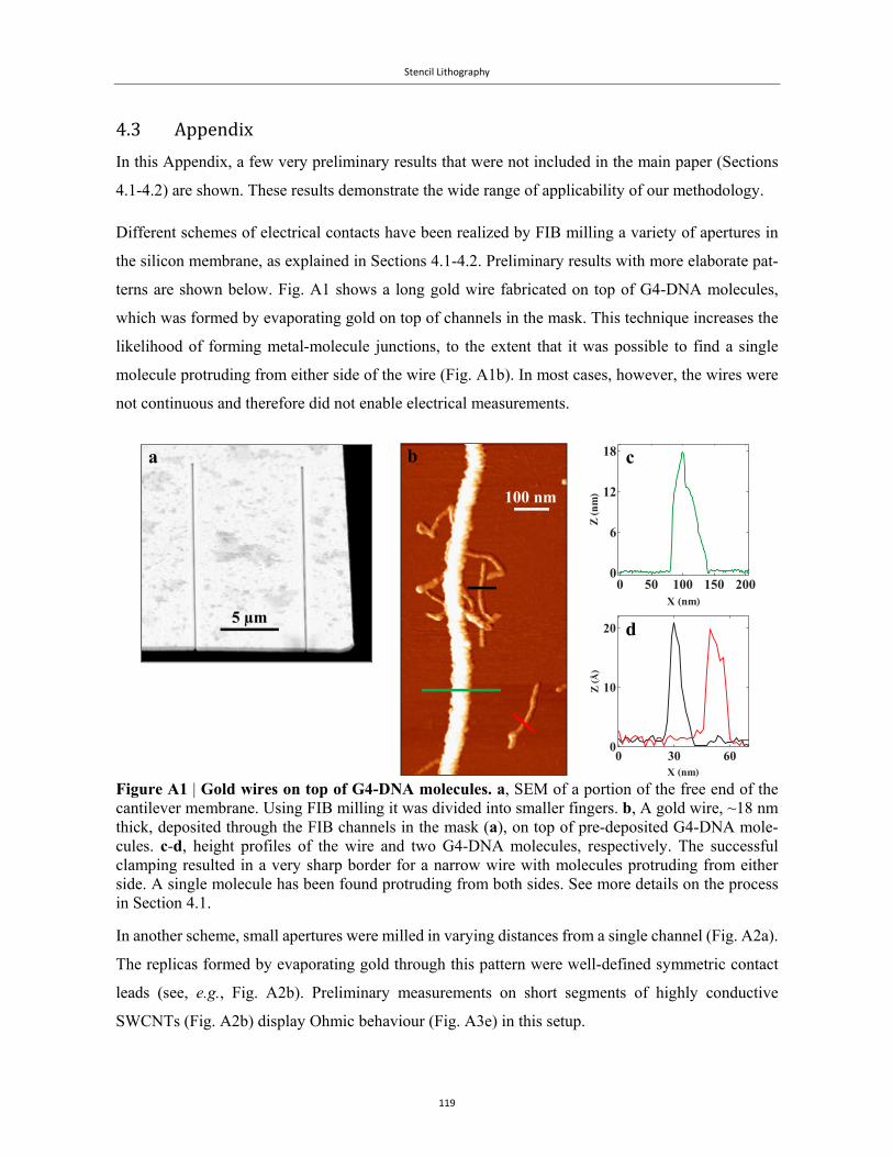
Stencil Lithography
119
4.3 Appendix
In this Appendix, a few very preliminary results that were not included in the main paper (Sections
4.1-4.2) are shown. These results demonstrate the wide range of applicability of our methodology.
Different schemes of electrical contacts have been realized by FIB milling a variety of apertures in
the silicon membrane, as explained in Sections 4.1-4.2. Preliminary results with more elaborate pat-
terns are shown below. Fig. A1 shows a long gold wire fabricated on top of G4-DNA molecules,
which was formed by evaporating gold on top of channels in the mask. This technique increases the
likelihood of forming metal-molecule junctions, to the extent that it was possible to find a single
molecule protruding from either side of the wire (Fig. A1b). In most cases, however, the wires were
not continuous and therefore did not enable electrical measurements.
Figure A1 | Gold wires on top of G4-DNA molecules. a, SEM of a portion of the free end of the cantilever membrane. Using FIB milling it was divided into smaller fingers. b, A gold wire, ~18 nm thick, deposited through the FIB channels in the mask (a), on top of pre-deposited G4-DNA mole-cules. c-d, height profiles of the wire and two G4-DNA molecules, respectively. The successful clamping resulted in a very sharp border for a narrow wire with molecules protruding from either side. A single molecule has been found protruding from both sides. See more details on the process in Section 4.1.
In another scheme, small apertures were milled in varying distances from a single channel (Fig. A2a).
The replicas formed by evaporating gold through this pattern were well-defined symmetric contact
leads (see, e.g., Fig. A2b). Preliminary measurements on short segments of highly conductive
SWCNTs (Fig. A2b) display Ohmic behaviour (Fig. A3e) in this setup.
100 nm
0 30 600
10
20
X nm
Z
0 50 100 150 2000
6
12
18
X nmZnm
c
d
b
5 µm
a
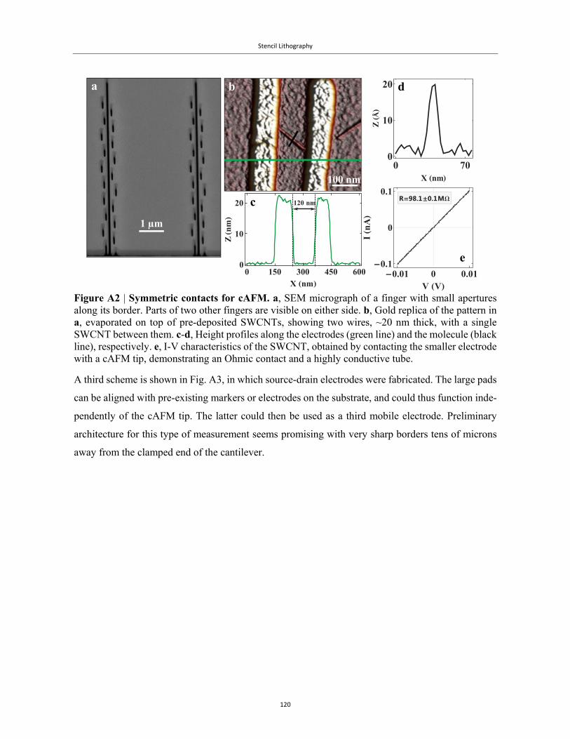
Stencil Lithography
120
Figure A2 | Symmetric contacts for cAFM. a, SEM micrograph of a finger with small apertures along its border. Parts of two other fingers are visible on either side. b, Gold replica of the pattern in a, evaporated on top of pre-deposited SWCNTs, showing two wires, ~20 nm thick, with a single SWCNT between them. c-d, Height profiles along the electrodes (green line) and the molecule (black line), respectively. e, I-V characteristics of the SWCNT, obtained by contacting the smaller electrode with a cAFM tip, demonstrating an Ohmic contact and a highly conductive tube.
A third scheme is shown in Fig. A3, in which source-drain electrodes were fabricated. The large pads
can be aligned with pre-existing markers or electrodes on the substrate, and could thus function inde-
pendently of the cAFM tip. The latter could then be used as a third mobile electrode. Preliminary
architecture for this type of measurement seems promising with very sharp borders tens of microns
away from the clamped end of the cantilever.
0 700
10
20
X nm
Z
100 nm
1 µm
0 150 300 450 6000
10
20
X nm
Znm
120 nm
a b
c
d
e0.0100.01
0.1
0
0.1
V V
InA
R98.10.1M
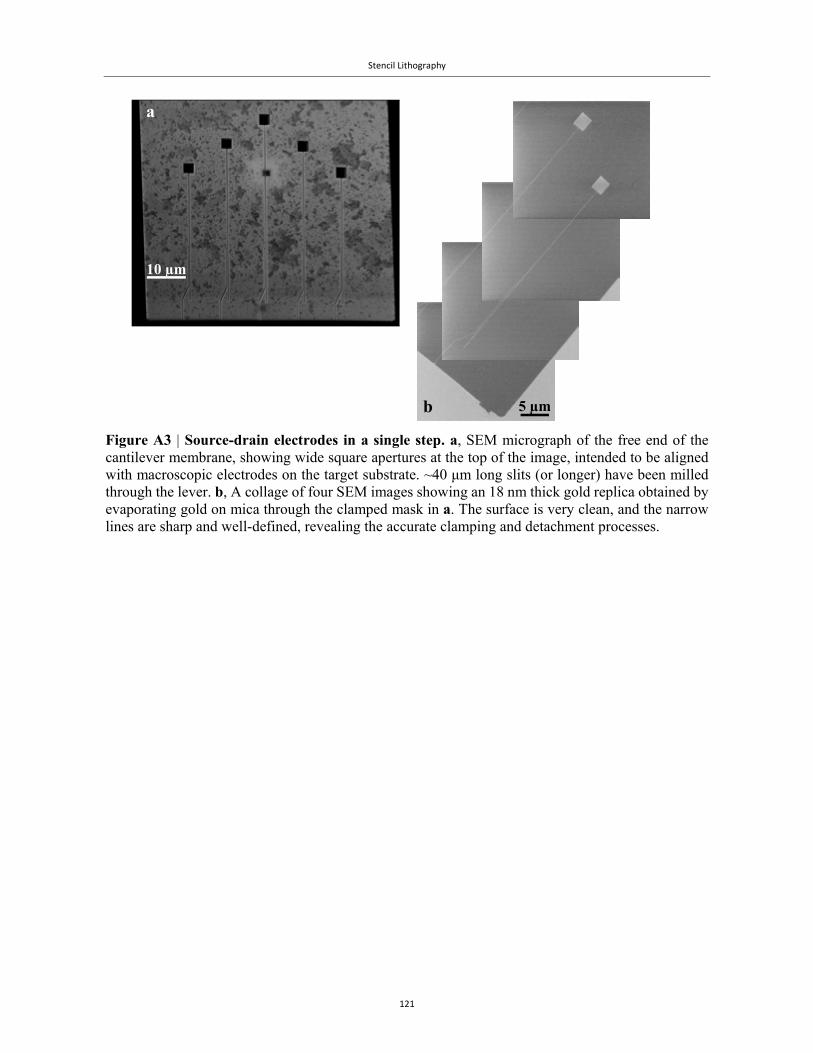
Stencil Lithography
121
Figure A3 | Source-drain electrodes in a single step. a, SEM micrograph of the free end of the cantilever membrane, showing wide square apertures at the top of the image, intended to be aligned with macroscopic electrodes on the target substrate. ~40 μm long slits (or longer) have been milled through the lever. b, A collage of four SEM images showing an 18 nm thick gold replica obtained by evaporating gold on mica through the clamped mask in a. The surface is very clean, and the narrow lines are sharp and well-defined, revealing the accurate clamping and detachment processes.
10 µm
5 µmb
a
122
General discussion, summary andconclusionsIn this work, individual G4-DNA molecules were placed on a solid mica substrate and measured
using EFM (Chapter 2). In other samples, strong and reliable coupling was formed between metal
electrodes and G4-DNA molecules, which were then measured by cAFM (Chapters 3 and 4). We got
clear and reproducible signs of folding-dependent polarizability1 (Chapter 2) as well as length-de-
pendent electrical conductivity that follows a thermally activated hopping mechanism2 (Chapter 3).
Moreover, we discovered that the way these strands were tied together also affected their electrical
properties1 (Chapters 2 and 3).
As we have mentioned in the Introduction and in Chapter 3, achievements in molecular electronics
have been mainly related to monolayers, sensors and electrical transport through short molecules. The
central challenges have remained. Namely, to transport current through long polymer wires, to un-
derstand the basic rules of this transport and to implement it in more complex electrical circuits. The
advanced methods developed during this PhD, and the results obtained with G4-DNA, represent a
major step forward in this direction, providing the most reliable and controlled platform for self-
assembled polymer-based solid-state devices. The long-range charge transport in G4-DNA – a com-
pletely organic DNA-based derivative – is the first controlled example of a single polymer wire that
can transport significant current over long distances when deposited on a hard substrate. Our results
and methodology pave the way for the implementation of DNA-based programmable circuits for
molecular electronics.
5.1 Achievedresults
We measured the electrostatic polarizability of G4-DNA as a function of its folding orientation. Irre-
spective of the EFM measurement setup parameters, and for two pairs of synthesized lengths, we
have found that both parallel and pairwise anti-parallel configurations of the strands were polarizable,
in accordance with previous measurements3,4 and that the parallel configuration was twice as polar-
izable as the pairwise anti-parallel one1 (Chapter 2). This suggests that the orientation of the backbone
strands strongly affects the π-π -stacking between the tetrads in the helix core5.
Summary
123
The origin of polarizability is typically attributed either to localized dipoles, which respond to the
external field by aligning themselves with the field, or to the induced movement of charges in the
molecule. These two extremes are characterized by very different time scales and mechanisms, since
for the former this is assumed to be ionic motion, while the latter is characterized by an electronic
response, which is typically much faster6.
In this regard, the origin of the EFM signal in G4-DNA was unclear. A plausible explanation was
some distortion of the guanine tetrads, as they responded to the electric field, which is clearly a more
localized ionic response. Nonetheless, the conductivity measurements (Chapter 3) produced highly
reproducible current-voltage characteristics, which were found to be compatible with thermally-acti-
vated long-range hopping between multi-tetrads blocks. This finding suggests that electronic pro-
cesses may account for the polarization, although a complementary dielectric response measurement
is required for a full analysis.
Our results indicate that structural and electrical properties are closely linked, and cannot be easily
disentangled for the quasi-1D wires we studied. The observation that molecular conformation affects
structural morphology, which in turn affects the electrical properties of G4-DNA, is not limited to
EFM observations.
The current-voltage characteristics presented in Chapter 3 were obtained from three different samples
prepared from the same batch of molecules. The charge transport in those molecules was highly bias-
dependent and was mainly limited by the interface rates, which were much smaller than the intra-
tetrad rate at high bias. Moreover, as mentioned in Chapter 3, the model suggests the following ex-
planation for the main features of the I-V curves: (i) the asymmetry in the I-Vs is due to the asymmetry
in the metal-molecule coupling, i.e., the contact at the evaporated electrode is much better and more
reproducible than the tip-molecule contact, which likely changes from point to point, and in turn leads
to an asymmetric voltage profile; (ii) the strong current suppression below a threshold voltage is due
to both the existence of an intrinsic gap in the molecule and the finite reorganization energy associated
with the charge injection in the molecule; (iii) the rapid rise of the current above the threshold reflects
the bias dependence of the injection rates, since the charge injection is the rate-limiting process at
high bias; (iv) the threshold depends weakly on the measured length of the molecule because the
voltage profile inside the molecule and, in turn, the energy of the relevant molecular levels depends
on this length; (v) the unusual length dependence of the current, which does not fit into any of the
standard length dependences, i.e., it is neither exponential nor a simple power law, stems from the
Summary
124
fact that the exact voltage profile also depends on the measured length of the molecule and this profile
affects both the intra-molecular rate and the metal-molecule interface rates.
The charge transport, based on the fit and on DFT calculations of the effective electronic coupling
between two adjacent tetrads, is consistent with an adiabatic mechanism, borderline with band
transport for reorganization energy values up to 1 eV (Chapter 3). Furthermore, the interplay between
the DFT calculations and the fit produced an inter-tetrad transfer rate of ~ 109 sec-1, consistent with
the model fit of k ~ 108 sec-1 over ten tetrads (which is the delocalization length, ~3.5 nm).
The most important technological achievement of this PhD work has been the methodology we de-
veloped for the formation of nanometre-sharp metal replicas, as described in detail in Chapter 4.
Though it was not the original focus of this research project, we explored the mechanisms of boundary
formation of thin metal films and metal penetration in our samples to improve our understanding of
the underlying mechanisms and improve our results. By studying the evolution of films with different
thicknesses under different clamping conditions, we have concluded that clamping by itself was not
sufficient to overcome the blurring effect. Crucially, in order to achieve sharp borders, it was neces-
sary to increase the bias – after contact was made – by an order of magnitude compared to the calcu-
lated pull-in value. This is most likely a result of fabrication variability, but more importantly, it
becomes clear that in order to avoid blurring, it is required in order to obtain a very tight contact
between the masking membrane and the substrate
The proposed mechanisms of penetration in the scientific literature, which are based on surface dif-
fusion7 and collisions with residual gas molecules8, did not seem to be supported by our findings. The
former approach, for example, yields a geometrical blurring (e.g., ~2.5 nm for a mask-substrate dis-
tance of ~100 nm) which is nearly two orders of magnitude smaller than the “shoulder” we have
observed in our samples (~250 nm). Furthermore, the temperature dependence of the penetration led
us to conclude that diffusion might aid the process (at elevated substrate temperatures) but was not
the dominant mechanism behind it.
Instead, we have found that the penetration of metal far beyond the border of the main replica could
be explained by collisions within the metal vapour and the disintegration of clusters in flight. Colli-
mation of the target did not reduce the penetration, suggesting that disintegration is the most probable
route by which the metal penetrates at oblique angles, forming isolated scattered islands even when
the replicas are well defined. As we noted in Chapter 4, this residual contamination occurs before the
mask-substrate gap is blocked, and is, in principle, unavoidable. Nonetheless, by a careful application
Summary
125
of the bias to the mask, we have routinely obtained very sharp replicas and nearly pristine substrates
beyond their borders for different substrates, metals and surface geometries. This technique may
prove useful in a variety of applications where cleaniness and precision are required, including li-
thography, ion-implantation, catalysis and nano-electronics.
5.2 Futureoutlook
We have used our methodology to investigate other molecules and objects, and have continued to
develop more advanced measurement techniques to address more complicated questions, as described
in the Appendix to Chapter 4. Below is a brief description of some possible future applications.
Preliminary measurements on a new batch of G4-DNA (see Appendix to Chapter 3 for details) indi-
cate G4-DNA is capable of transporting higher current at longer distances (e.g. ~350 pA at ~200 nm).
This is a possible indication of its broad potential in the development of G4-DNA-based devices and
their incorporation into solid-state microelectronics. Therefore, we believe that the present thesis does
not terminate but rather only initiate the study into the transport properties of these molecules, and
will form the basis for future investigations.
The asymmetry in the current-voltage characteristics in tetra-molecular G4-DNA (Chapter 3) has
been attributed, within the scope of our hopping model, to the asymmetry of the contacts. Notwith-
standing, some contribution to the asymmetry could also be molecular in origin, e.g., related to the
folding orientation of the constitutive guanine strands, which has already been shown in Chapter 2 to
induce changes in morphology and polarizability in G4-DNA. To resolve this issue, we fabricated
two types of contacts by FIB milling different apertures into the lever. These patterns and their cor-
responding replicas enable to form symmetric stationary contacts with various separations (see, for
example, Section 4.3, Fig. A2). Such modifications to the standard cAFM technique should form
strong electrical coupling on either end of the molecule, as demonstrated in Chapter 3.
We have seen in Chapter 2 that both tetra- and intra-molecular G4-DNA respond to an external elec-
tric field. This response is a promising venue to explore with gate measurements. How might the
transport through these molecules be affected by an external field? To test this experimentally, we
created symmetric source-drain contacts, which would function independently of the cAFM tip. The
latter could then be used as a third mobile gate electrode. Preliminary architecture (Section 4.3, Fig.
A3) for this type of measurement seems promising with very sharp borders tens of microns away
from the clamped end of the cantilever. Gate measurements would allow to induce local change in
the molecule, influence its energy levels and charge mobility, and possibly unlock more information
Summary
126
on the charge transport within the molecule. An additional probe may be used for other purposes as
well, such as heat transfer and optical measurements in conjunction with direct electrical measure-
ments
References
1 Livshits, G. I., Ghabboun, J., Borovok, N., Kotlyar, A. & Porath, D. Comparative EFM of mono‐ and tetra‐molec‐ular G4‐DNA. Adv Mater 26, 4981‐4985 (2014).
2 Livshits, G. I. et al. Long‐range charge transport in single G‐quadruplex DNA molecules. Nat Nanotechnol In Press (2014).
3 Cohen, H. et al. Polarizability of G4‐DNA observed by electrostatic force microscopy measurements. Nano Lett 7, 981‐986 (2007).
4 Borovok, N. et al. Assembling of G‐strands into novel tetra‐molecular parallel G4‐DNA nanostructures using avidinbiotin recognition. Nucleic Acids Res 36, 5050‐5060 (2008).
5 Lech, C. J., Phan, A. T., Michel‐Beyerle, M. E. & Voityuk, A. A. Electron‐Hole Transfer in G‐Quadruplexes with Different Tetrad Stacking Geometries: A Combined QM and MD Study. J Phys Chem B 117, 9851‐9856 (2013).
6 Takashima, S. Electrical Properties of Biopolymers and Membranes. (Adam Hilger, 1989). 7 Vazquez‐Mena, O. et al. Analysis of the blurring in stencil lithography. Nanotechnology 20, 415303 (2009). 8 Podzorov, V., Sysoev, S. E., Loginova, E., Pudalov, V. M. & Gershenson, M. E. Single‐crystal organic field effect
transistors with the hole mobility similar to 8 cm(2)/V s. Appl Phys Lett 83, 3504‐3506 (2003).
תקציר
א
תקצירעל מנת , G4‐DNA פרטהתכונות החשמליות של נגזרות דנ"א שונות, ובדיסרטציה זו מציגה את תוצאות מחקר
.לגלות ולהבין את מנגנוני המוליכות בחוטים אלו
, המריץ אלקטרונייםמטריים המוליכים חשמל, אשר יכולים להשתלב בהתקנים -ר חוטים ננוהחיפוש אח
גדילי, שהיווה דוגמא מרכזית לפולימר חד ממדי -והעמיק את המחקר אודות התכונות החשמליות של דנ"א דו
נחשב ליבת הבסיסים של המולקולה לאורך π-πלי מסוג . הצימוד האורביט1,2בעל מבניות הניתנת לתכנות
ותלותה בסביבה בה נמצאת מורכבותה של ההולכה החשמלית . אולם 3לאפיק חשמלי דרכו המטען יכול לעבור
גדילי ארוך הצמוד -. כך למשל, אנו יודעים היום שדנ"א דולא נלקחו בחשבון בהיבט הפרקטי 7-4המולקולה
גוון רחב של תוצאות הובילו למ. יתרה מזאת, הניסויים השונים בתחום 12-8למשטח מוצק אינו מוליך במצב יבש
פולימרים בודדים , ובכך הדגישו את האתגר הגלום במדידה מהימנה של 16-13סותרות זו את זושלכאורה חלקיות
דידות אמינות, שבהן ניתן לזהות מולקולה פולימרית בודדת עד כה לא פורסמו מ .בכלל ומולקולות אלו בפרט
באורך של עשרות ננומטרים לפחות, הספוחה על גבי משטח קשיח, למדוד מעבר זרם חשמלי דרכה באופן הדיר
ותלוי ארך ולקבוע את מנגנון ההולכה החשמלי הדומיננטי.
א, המורכבת מארבעה גדילים של הבסיס בכדי להתמודד עם אתגרים אלה, התמקדנו בנגזרת מלאכותית של דנ"
G4-( . ארבעת הגדילים, המלופפים זה סביב זה בצורת בורג, יוצרים חוט חד ממדי אחיד19-17)Guanineגואנין (
DNA( , חידה בפני עיוותים משטחיים. המבנה המחזורי האחיד מורכב מייחסית עמיד למדי שהוא קשיח
סונתזו ע"י שותפינו למחקר. G4-DNA. שני סוגים שונים של G, המורכבת מארבעת יחידות טטראדההנקראת
באותו הכיוון שכולםעם ארבעה גדילים מקבילים, G4-DNAהם נבדלים זה מזה בכיוון הקיפול של הגדילים.
מחובר למולקולת ביוטין). כל גדיל tetra-molecular (tm)G4-DNAמולקולארי (-טטרא G4-DNAנקרא
)biotin) וכל ביוטין מתחבר ליחידה נפרדת באבידין ,(avidin(19 סוג אחר של .DNA-G4 מתקבל ע"י קיפול של
בכיוון מכוונים נוגדת, כך ששני גדילים ות מגדיל בודד שלוש פעמים. קיפול כזה יוצר ארבעה גדילים בעלי כיווני
-intraמולקולארי (-אינטרה G4-DNAמסוג זה מכונה G4-DNAאחד, בעוד שהשניים האחרים בכיוון ההפוך.
DNA-molecular (im)G4(17,18.
. שיטת 20גדילי-ובין דנ"א דו DNA-imG4עבודות קודמות שנעשו במעבדתנו השוו את הקיטוב החשמלי בין
צבת החוד המוליך מעליה. החוד ) בוחנת את התגובה של המולקולה לשדה חשמלי ע"י הEFMהקיטוב החשמלי (
ע"י מדידת הפרש הפאזה. הקיטוב החשמלי יכול להעיד ה של המולקולה את השדה, ואף מודד את תגובת משרה
תוצאות לה בודדת להוליך חשמל. על ניידות המטען, ועל כן יכול בצורה עקיפה להעיד על יכולתה של מולקו
במסגרת . גדילי אינו מקוטב-מקוטב, בעוד שדנ"א דו במרכזו) עם יוני אשלגן( imG4-DNA –המחקר הראו ש
. בעזרת מיקרוסקופ G4-DNAהעבודה הנוכחית התקדמנו שלב נוסף, והשווינו בין שני הסוגים השונים של
תקציר
ב
שעבור מספר זהה של ,19, בהתאמה לעבודה קודמת במעבדתנו21הראינו בצורה מבוקרת), AFMאטומי סורק (
. זאת ועוד, הקיטוב החשמלי במבנה imG4-DNA –מעט קצר יותר מ גבוה יותר ו tmG4-DNAטטראדות,
פירושו של דבר שכיווניות הגדילים כנראה . 21מקביל-המקביל הינו פי שניים חזק יותר מאשר במבנה האנטי
על המבנה הפנימי, קרי על הטטראדה הבודדת ועל הסידור מבנה המרחבי של המולקולה, ובפרט משפיעה על ה
. פועל יוצא הוא שהמבנה המקביל רגיש יותר לשדה החשמלי, ביניהן π –, ולכן על צימוד ה המבני בין הטטראדות
הולכה חשמליות. מועמד טוב יותר למדידות לכןו
השתמשנו במיקרוסקופ אטומי סורק בעל חוד מוליך , tmG4-DNA –על מנת לבצע מדידות חשמליות ישירות ב
)cAFMספוחה). מערך זה כולל שלושה מרכיבים מרכזיים. הראשון הוא האובייקט הנמדד, קרי המולקולה ה
חשמלי אחד נוצר על ידי נידוף תרמי של זהב על גבי משטח מבודד חשמלית. השני הוא המגעים החשמליים. מגע
המשטח באזור הגבול על פני חלק מן המולקולה. מגע חשמלי שני נוצר על ידי החוד המוליך, המאפשר לסרוק את
ישירות, ובו זמנית למדוד המתכתי המנודף ולנטר מולקולות היוצאות ממנו, וליצור מגע חשמלי עם כל אחת מהן
. הרכיב השלישי הוא כמובן מערכת המדידה, היוצרת את הפרש המתחים, ומודדת את האופיין החשמלי שלה
של המולקולה. מערך ניסיוני זה יוצר קשר חשמלי חזק למולקולה, במיוחד במגע החשמלית את התגובה
המנודף, ומאפשר לבחון את התלות האורכית של המוליכות לאור הניידות של החוד המוליך.
. 22ה חלק מהמולקולה, מתקבל ע"י נידוף דרך מסכה קשיחה המונחת על פני המשטחהמגע המנודף, אשר מכס
. לאחר הנידוף, מסירים את המסכה, ועל פני המשטח מוגדרים היטב וחדיםלמסכה זו צריכים להיות גבולות
נוצר תבליט מתכתי. בהינתן צפיפות משטחית מספקת, ניתן לאתר מולקולות המבצבצות מתחת לשפת התבליט.
ניתן ליצור מגע ולחלק זה ,מתכת, ואולם יש להן גם חלק חשוףשכבת הבמולקולות אלה מכוסות באופן חלקי
התבליט הזו מתאימה במיוחד יצירת החוד הסורק המוליך. באופן כזה נסגר המעגל החשמלי. שיטת עם
למדידות של חומרים אורגניים או ביולוגיים, הרגישים לשיטות ליתוגרפיות סטנדרטיות, שבהן מעורבים בדר"כ
מרים העלולים לפגום באלמנט הרגיש.שלל חו
התבליט המתוארת לעיל קיים חיסרון משמעותי. בין המסכה והמשטח יצירת ליה וקוץ בה. בשיטת ואולם, א
שכבה. חדירה זו מונעת יצירתם של גבולות חדים ב25-23קיים מרווח, שדרכו חודרת המתכת המתנדפת
ין את האובייקט הנמדד, ולהשפיע באופן בלתי ידוע , וכתוצאה מכך המתכת עלולה לכסות לחלוטתהמתכתי
ובלתי נשלט על המוליכות שלו. בכדי להתגבר על מגבלה זו, פיתחנו שיטה המאפשרת להצמיד את המסכה אל
הדגם במהלך תהליך הנידוף באמצעות 'הצמדה אלקטרוסטטית'. עיקרון פעולתה שקול לעקרון הפעולה של קבל
(הדגם) והשני גמיש (המסכה). טעינת הקבל גורמת ללוח הגמיש להתכופף לעבר לוחות, שאחד מלוחותיו קשיח
-המשיכה החשמלית. כיפוף זה אינו לינארי, ובעיוות מסוים של הלוח הגמיש מתגבשת איבגלל הלוח הקשיח
היציבות הזו, והדגמנו -, המאלצת אותו לקפוץ למגע עם המשטח התחתון. אנו ניצלנו את אי26,27יציבות מבנית
דגמים הביא לפיתוח ם מישוריים ועקומים. יתר על כן, מחקר זהבעבודתנו הצמדה מושלמת של המסכה לשטחי
עים מנודפים מוגדרים היטב,ע"י יצירה של שני מג cAFM –שיטת ה מתקדמים יותר שלהמאפשרים שימושים
וסיפק תובנה הן לתהליך היצמדות המסכה והן לתהליכיי החדירה ויצירת שפת התבליט.
מטריים, -השתמשנו בשיטה זו על מנת לחקור את התכונות החשמליות של שלל מולקולות או חוטים ננו
), רשתות SWCNTה בודדת (, צינוריות פחמן קצרות בעלות שכבtmG4‐DNAגדילי ארוך, -וביניהם: דנ"א דו
תקציר
ג
זוגות של 26מטריים המורכבים מדנ"א קצר (בעל -מבנים ננו) וMWCNTשכבתיות (-של צינוריות פחמן רב
.SWCNT-dsDNA-SWCNT –בסיסים)
ע"י מדידת האופיין החשמלי בנקודות DNA-tmG4 –הצלחנו להתחקות אחר מנגנון ההולכה החשמלית ב
HOPPINGשל ההתנגדות החשמלית, המתאימה למנגנון ית. גילינו תלות אורכ28שונות על פני המולקולות
–אמפר עד מעבר ל -לטווח ארוך התלוי בטמפרטורה. במסגרת ניסויים אלה, מדדנו זרמים שנעו בין מס' פיקו
pA 100 נ"מ מגבול השפה המנודפת. 100 –ולמרחקים מעשרות ועד כ
מאפשרת לספק שפיתחנו אפשרה מדידות הדירות של זרמים, וכתוצאה מכך להכנת הדגמים השיטה הייחודית
גבוהים יותר במרחקיםזרמים מסוג חדש הראו tmG4-DNA מולקלות בודדות של שותפינו.טוב יותר למשוב
גדילי -. מדידות דומות על דנ"א דונ"מ 150 –במרחק של כ pA 350 –כ ארוכים יותר, למשל באחד מהמקרים
הראו שהוא מבודד, בעוד שצינוריות הפחמן הראו הולכה אוהמית, המתאימה לתכונותיהן הידועות. מדידות
הראו מגוון רחב של ,SWCNT-dsDNA-SWCNT בקונפיגורציה מולקולות דנ"א קצרותמספר ראשוניות על
לתצורות השונות של המבנה המורכב. תוצאות, המיוחסות
:תוצאות ושיטות מרכזיות
מעידות על שינויים מורפולוגיים ורגישות tmG4-DNA –ו imG4-DNAשל EFM –ו AFMת והשווא .1
ה שונה לשדה החשמלי, ומצביעות על השפעת כיווניות הגדיל על המבנה המולקולארי, קרי הטטראד
הבודדת, המבנה המרחבי בין הטטראדות, והקיטוב החשמלי.
2. tmG4-DNA מקוטב פי שניים מ– imG4-DNA.
המבוסס ,ך טווחור, המתאימה למנגנון הולכה אtmG4-DNA –ארוכת טווח נמדדה ב הולכה חשמלית .3
אמפר עד מעבר -תרמי בין קבוצות של מס' טטראדות. נמדדו זרמים שנעו בין מס' פיקו HOPPINGעל
נ"מ מגבול השפה המנודפת. 100 –ולמרחקים מעשרות ועד כ pA 100 –ל
מכאנית הפיכה של המסכה לדגם, המתגברת על -פותחה שיטה חדשה המבוססת על הצמדה אלקטרו .4
,הצמדה מושלמת של המסכה למשטחמאפשרת ה ,ושיטה ז החדירה המתכתית הבעייתית הידועה.
היציבות המבני הודגם בתוך -תחום אי .)SEMמקרוסקופ אלקטרון סורק (ו AFMהודגמה באמצעות
SEM.והומחש ע"י חשבון הענות מעבר לא לינארית ,
–שיטת ה דגמים ייחודיים שהכנו בעזרת השיטה שלעיל אפשרו מדידות חדשות וניצול מיטבי של .5
cAFM ם מס' שינויים, ובכלל זה ע"י יצירה של מגעים חשמליים מנודפים סימטריים.ע
הצענו מנגנונים חדשים להסבר החדירה המתכתית ויצירת השפה, המבוססים על נידוף צבירים .6
והתפרקותם תוך כדי מעוף. מנגנונים אלה הצליחו להסביר איכותית את גבול הרזולוציה בשיטת נידוף
דרך מסכה.
תקציר
ד
גרפיהביבליו
1 Seeman, N. C. DNA in a material world. Nature 421, 427‐431 (2003)
2 Seeman, N. C. An overview of structural DNA Nanotechnology. Mol Biotechnol 37, 246‐257 (2007)
3 Bixon, M. et al. Long‐range charge hopping in DNA. P Natl Acad Sci USA 96, 11713‐11716 (1999)
4 Kasumov, A. Y., Klinov, D. V., Roche, P. E., Gueron, S. & Bouchiat, H. Thickness and low‐temperature conductivity of DNA molecules. Appl Phys Lett 84, 1007‐1009 (2004)
5 Heim, T., Deresmes, D. & Vuillaume, D. Conductivity of DNA probed by conducting‐atomic force microscopy: Effects of contact electrode, DNA structure, and surface interactions. J Appl Phys 96, 2927‐2936 (2004)
6 Gutierrez, R., Porath, D. & Cuniberti, G. in Charge Transport in Disorderd Solids with Applications in Electronics ed Sergei Baranovski) (Wiley, 2006)
7 Cai, L. T., Tabata, H. & Kawai, T. Probing electrical properties of oriented DNA by conducting atomic force micros‐ copy. Nanotechnology 12, 211‐216 (2001)
8 Storm, A. J., van Noort, J., de Vries, S. & Dekker, C. Insulating behavior for DNA molecules between nanoelectrodes at the 100 nm length scale. Appl Phys Lett 79, 3881‐3883 (2001)
9 Braun, E., Eichen, Y., Sivan, U. & Ben‐Yoseph, G. DNA‐templated assembly and electrode attachment of a conduct‐ ing silver wire. Nature 391, 775‐778 (1998)
10 de Pablo, P. J. et al. Absence of dc‐conductivity in lambda‐DNA. Phys Rev Lett 85, 4992‐4995 (2000)
11 Bockrath, M. et al. Scanned conductance microscopy of carbon nanotubes and lambda‐DNA. Nano Lett 2, 187‐ 190 (2002)
12 Gomez‐Navarro, C. et al. Contactless experiments on individual DNA molecules show no evidence for molecular wire behavior. P Natl Acad Sci USA 99, 8484‐8487 (2002)
13 Astakhova, T. Y., Likhachev, V. N. & Vinogradov, G. A. Long‐range charge transfer in biopolymers. Russ Chem Rev+ 81, 994‐1010 (2012)
14 Endres, R. G., Cox, D. L. & Singh, R. R. P. Colloquium: The quest for high‐conductance DNA. Rev Mod Phys 76, 195‐ 214 (2004)
15 Porath, D., Cuniberti, G. & Di Felice, R. Charge transport in DNA‐based devices Top Curr Chem 237, 183‐227 (2004)
16 Muren, N. B., Olmon, E. D. & Barton, J. K. Solution, surface, and single molecule platforms for the study of DNA‐ mediated charge transport. Phys Chem Chem Phys 14, 13754‐13771 (2012)
17 Kotlyar, A. B. et al. Long, monomolecular guanine‐based nanowires. Adv Mater 17, 1901‐1904 (2005)
18 Borovok, N., Molotsky, T., Ghabboun, J., Porath, D. & Kotlyar, A. Efficient procedure of preparation and properties of long uniform G4‐DNA nanowires. Anal Biochem 374, 71‐78 (2008)
19 Borovok, N. et al. Assembling of G‐strands into novel tetra‐molecular parallel G4‐DNA nanostructures using avi‐ dinbiotin recognition. Nucleic Acids Res 36, 5050‐5060 (2008) 20 Cohen, H. et al. Polarizability of G4‐DNA observed by electrostatic force microscopy measurements. Nano Lett 7, 981‐986 (2007)
21 Livshits, G. I., Ghabboun, J., Borovok, N., Kotlyar, A. & Porath, D. Comparative EFM of mono‐ and tetra‐molecular G4‐DNA. Adv Mater 26, 4981‐4985 (2014)
22 Deshmukh, M. M., Ralph, D. C., Thomas, M. & Silcox, J. Nanofabrication using a stencil mask. Appl Phys Lett 75, 1631‐1633 (1999)
23 Podzorov, V., Sysoev, S. E., Loginova, E., Pudalov, V. M. & Gershenson, M. E. Single‐crystal organic field effect transistors with the hole mobility similar to 8 cm(2)/V s. Appl Phys Lett 83, 3504‐3506 (2003)
24 Racz, Z. & Seabaugh, A. Characterization and control of unconfined lateral diffusion under stencil masks. J Vac Sci Technol B 25, 857‐861 (2007)
25 Vazquez‐Mena, O. et al. Analysis of the blurring in stencil lithography. Nanotechnology 20, 415303 (2009)
26 Rebeiz, G. M. RF MEMS: Theory, Design and Technology. (John Wiley & Sons, 2003) 27 Senturia, S. D. Microsystem Design. (Kluwer Academic Pulishers, 2002) 28 Livshits, G. I. et al. Long‐range charge transport in single G‐quadruplex DNA molecules. Nat Nanotechnol In Press (2014)

עבודה זו נעשתה בהדרכתו של
פרופ' דני פורת
פיתוח שיטות אפיון ומדידות חדשניות של תכונות
זרות של דנ"אונג G4-DNAחשמליות של
חיבור לשם קבלת תואר דוקטור לפילוסופיה
מאת
גדעון ליבשיץ
הוגש לסנאט האוניברסיטה העברית בירושלים
2014 קטובראו
פיתוח שיטות אפיון ומדידות חדשניות של תכונות
ונגזרות של דנ"א G4-DNAחשמליות של
חיבור לשם קבלת תואר דוקטור לפילוסופיה
מאת
גדעון ליבשיץ
הוגש לסנאט האוניברסיטה העברית בירושלים
2014 קטובראו