Embed Size (px)
Citation preview
This is information on a product in full production.
October 2017 DocID030747 Rev 1 1/32
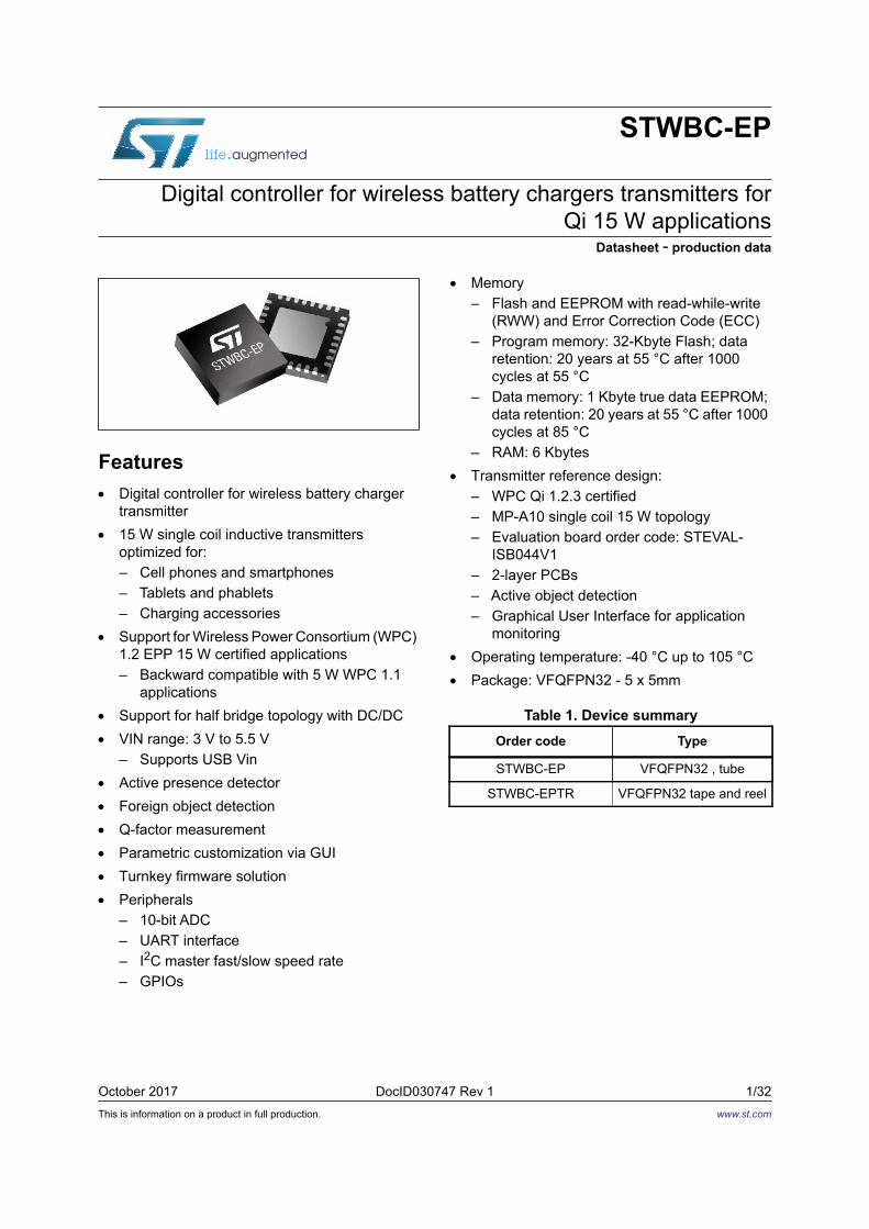
STWBC-EP
Digital controller for wireless battery chargers transmitters forQi 15 W applications
Datasheet - production data
Features Digital controller for wireless battery charger
transmitter 15 W single coil inductive transmitters
optimized for:– Cell phones and smartphones– Tablets and phablets– Charging accessories
Support for Wireless Power Consortium (WPC) 1.2 EPP 15 W certified applications– Backward compatible with 5 W WPC 1.1
applications Support for half bridge topology with DC/DC VIN range: 3 V to 5.5 V
– Supports USB Vin Active presence detector Foreign object detection Q-factor measurement Parametric customization via GUI Turnkey firmware solution Peripherals
– 10-bit ADC– UART interface– I2C master fast/slow speed rate– GPIOs
Memory– Flash and EEPROM with read-while-write
(RWW) and Error Correction Code (ECC)– Program memory: 32-Kbyte Flash; data
retention: 20 years at 55 °C after 1000 cycles at 55 °C
– Data memory: 1 Kbyte true data EEPROM; data retention: 20 years at 55 °C after 1000 cycles at 85 °C
– RAM: 6 Kbytes Transmitter reference design:
– WPC Qi 1.2.3 certified– MP-A10 single coil 15 W topology– Evaluation board order code: STEVAL-
ISB044V1– 2-layer PCBs– Active object detection– Graphical User Interface for application
monitoring Operating temperature: -40 °C up to 105 °C Package: VFQFPN32 - 5 x 5mm
Table 1. Device summaryOrder code Type
STWBC-EP VFQFPN32 , tube
STWBC-EPTR VFQFPN32 tape and reel
www.st.com
Contents STWBC-EP
2/32 DocID030747 Rev 1
Contents
1 Description . . . . . . . . . . . . . . . . . . . . . . . . . . . . . . . . . . . . . . . . . . . . . . . . . 6
2 STWBC-EP system architecture . . . . . . . . . . . . . . . . . . . . . . . . . . . . . . . 7Firmware . . . . . . . . . . . . . . . . . . . . . . . . . . . . . . . . . . . . . . . . . . . . . . . . . . . . . . . . . 7
3 Reference design . . . . . . . . . . . . . . . . . . . . . . . . . . . . . . . . . . . . . . . . . . . 8
4 STWBC-EP pinout and pin description . . . . . . . . . . . . . . . . . . . . . . . . . . 9
5 Pins functional description . . . . . . . . . . . . . . . . . . . . . . . . . . . . . . . . . . 115.1 Power supplies: VDD, VDDA, VSS, VSSA, VOUT . . . . . . . . . . . . . . . . . . 11
5.2 DC/DC converter: DCDC_DRV, DCDC_DAC, CMP_OUT_V, CS_CMP, DCDC_DAC_REF, DEMAGNET, VTARGET . . . . . . . . . . . . . . . . . . . . . . 11
5.3 Half bridge driver: UPBL, DNBL, PWM_QFOD, WAVE_SNS . . . . . . . . . 12
5.4 Wireless power functions: TANK_VOLTAGE, ISENSE, COIL_TEMP, SYMBOL_DETECT, CURRENT_DEMOD, CS_CMP_AVG . . . . . . . . . . . 12
5.5 Input power supply management: VMAIN, QC_IO . . . . . . . . . . . . . . . . . . 13
5.6 External digital interface: UART_TX, UART_RX . . . . . . . . . . . . . . . . . . . 13
5.7 End user signaling: LED . . . . . . . . . . . . . . . . . . . . . . . . . . . . . . . . . . . . . . 13
5.8 Expansion interface: I2C_SDA, I2C_SCL . . . . . . . . . . . . . . . . . . . . . . . . 13
5.9 Debug: SWIM, NRST . . . . . . . . . . . . . . . . . . . . . . . . . . . . . . . . . . . . . . . . 13
6 Electrical characteristics . . . . . . . . . . . . . . . . . . . . . . . . . . . . . . . . . . . . 146.1 Parameter conditions . . . . . . . . . . . . . . . . . . . . . . . . . . . . . . . . . . . . . . . . 14
6.2 Minimum and maximum values . . . . . . . . . . . . . . . . . . . . . . . . . . . . . . . . 14
6.3 Typical values . . . . . . . . . . . . . . . . . . . . . . . . . . . . . . . . . . . . . . . . . . . . . . 14
6.4 Typical curves . . . . . . . . . . . . . . . . . . . . . . . . . . . . . . . . . . . . . . . . . . . . . . 14
6.5 Typical current consumption . . . . . . . . . . . . . . . . . . . . . . . . . . . . . . . . . . . 14
6.6 Loading capacitors . . . . . . . . . . . . . . . . . . . . . . . . . . . . . . . . . . . . . . . . . . 15
6.7 Pin output voltage . . . . . . . . . . . . . . . . . . . . . . . . . . . . . . . . . . . . . . . . . . . 15
6.8 Absolute maximum ratings . . . . . . . . . . . . . . . . . . . . . . . . . . . . . . . . . . . . 16
6.9 Operating conditions . . . . . . . . . . . . . . . . . . . . . . . . . . . . . . . . . . . . . . . . 176.9.1 VOUT external capacitor . . . . . . . . . . . . . . . . . . . . . . . . . . . . . . . . . . . . 18
DocID030747 Rev 1 3/32
STWBC-EP Contents
32
6.9.2 Memory characteristics . . . . . . . . . . . . . . . . . . . . . . . . . . . . . . . . . . . . . 19
6.9.3 I/O port pin characteristics . . . . . . . . . . . . . . . . . . . . . . . . . . . . . . . . . . . 20
6.9.4 Typical output level curves . . . . . . . . . . . . . . . . . . . . . . . . . . . . . . . . . . . 22
6.9.5 Reset pin characteristics . . . . . . . . . . . . . . . . . . . . . . . . . . . . . . . . . . . . 24
6.9.6 I2C interface characteristics . . . . . . . . . . . . . . . . . . . . . . . . . . . . . . . . . . 24
6.9.7 10-bit SAR ADC characteristics . . . . . . . . . . . . . . . . . . . . . . . . . . . . . . . 25
7 Thermal characteristics . . . . . . . . . . . . . . . . . . . . . . . . . . . . . . . . . . . . . 28
8 Package information . . . . . . . . . . . . . . . . . . . . . . . . . . . . . . . . . . . . . . . . 298.1 VFQFPN32 package information . . . . . . . . . . . . . . . . . . . . . . . . . . . . . . . 29
9 Revision history . . . . . . . . . . . . . . . . . . . . . . . . . . . . . . . . . . . . . . . . . . . 31
List of tables STWBC-EP
4/32 DocID030747 Rev 1
List of tables
Table 1. Device summary . . . . . . . . . . . . . . . . . . . . . . . . . . . . . . . . . . . . . . . . . . . . . . . . . . . . . . . . . . 1Table 2. Pinout description . . . . . . . . . . . . . . . . . . . . . . . . . . . . . . . . . . . . . . . . . . . . . . . . . . . . . . . . . 9Table 3. Voltage characteristics . . . . . . . . . . . . . . . . . . . . . . . . . . . . . . . . . . . . . . . . . . . . . . . . . . . . 16Table 4. Current characteristics . . . . . . . . . . . . . . . . . . . . . . . . . . . . . . . . . . . . . . . . . . . . . . . . . . . . 16Table 5. Thermal characteristics. . . . . . . . . . . . . . . . . . . . . . . . . . . . . . . . . . . . . . . . . . . . . . . . . . . . 16Table 6. General operating conditions . . . . . . . . . . . . . . . . . . . . . . . . . . . . . . . . . . . . . . . . . . . . . . . 17Table 7. Operating conditions at power-up/power-down . . . . . . . . . . . . . . . . . . . . . . . . . . . . . . . . . 17Table 8. Flash program memory/data EEPROM memory . . . . . . . . . . . . . . . . . . . . . . . . . . . . . . . . 19Table 9. Voltage DC characteristics . . . . . . . . . . . . . . . . . . . . . . . . . . . . . . . . . . . . . . . . . . . . . . . . . 20Table 10. Current DC characteristics . . . . . . . . . . . . . . . . . . . . . . . . . . . . . . . . . . . . . . . . . . . . . . . . . 21Table 11. NRST pin characteristics . . . . . . . . . . . . . . . . . . . . . . . . . . . . . . . . . . . . . . . . . . . . . . . . . . 24Table 12. I2C interface characteristics . . . . . . . . . . . . . . . . . . . . . . . . . . . . . . . . . . . . . . . . . . . . . . . . 24Table 13. ADC characteristics . . . . . . . . . . . . . . . . . . . . . . . . . . . . . . . . . . . . . . . . . . . . . . . . . . . . . . 25Table 14. ADC accuracy characteristic at VDD/VDDA = 5 V . . . . . . . . . . . . . . . . . . . . . . . . . . . . . . . . 25Table 15. Thermal characteristics. . . . . . . . . . . . . . . . . . . . . . . . . . . . . . . . . . . . . . . . . . . . . . . . . . . . 28Table 16. VFQFPN32 package mechanical data . . . . . . . . . . . . . . . . . . . . . . . . . . . . . . . . . . . . . . . . 30Table 17. Document revision history. . . . . . . . . . . . . . . . . . . . . . . . . . . . . . . . . . . . . . . . . . . . . . . . . . 31
DocID030747 Rev 1 5/32
STWBC-EP List of figures
32
List of figures
Figure 1. Wireless charging system description. . . . . . . . . . . . . . . . . . . . . . . . . . . . . . . . . . . . . . . . . . 6Figure 2. STWBC-EP device architecture . . . . . . . . . . . . . . . . . . . . . . . . . . . . . . . . . . . . . . . . . . . . . . 7Figure 3. STEVAL-ISB044V1 evaluation board . . . . . . . . . . . . . . . . . . . . . . . . . . . . . . . . . . . . . . . . . . 8Figure 4. STWBC-EP configuration . . . . . . . . . . . . . . . . . . . . . . . . . . . . . . . . . . . . . . . . . . . . . . . . . . . 9Figure 5. Supply current measurement conditions. . . . . . . . . . . . . . . . . . . . . . . . . . . . . . . . . . . . . . . 15Figure 6. Pin loading conditions. . . . . . . . . . . . . . . . . . . . . . . . . . . . . . . . . . . . . . . . . . . . . . . . . . . . . 15Figure 7. Pin input voltage . . . . . . . . . . . . . . . . . . . . . . . . . . . . . . . . . . . . . . . . . . . . . . . . . . . . . . . . . 15Figure 8. External capacitor CVOUT . . . . . . . . . . . . . . . . . . . . . . . . . . . . . . . . . . . . . . . . . . . . . . . . . . 18Figure 9. VOH standard pad at 3.3 V . . . . . . . . . . . . . . . . . . . . . . . . . . . . . . . . . . . . . . . . . . . . . . . . . 22Figure 10. VOL standard pad at 3.3 V . . . . . . . . . . . . . . . . . . . . . . . . . . . . . . . . . . . . . . . . . . . . . . . . . 22Figure 11. VOH standard pad at 5 V. . . . . . . . . . . . . . . . . . . . . . . . . . . . . . . . . . . . . . . . . . . . . . . . . . . 22Figure 12. VOL standard pad at 5 V . . . . . . . . . . . . . . . . . . . . . . . . . . . . . . . . . . . . . . . . . . . . . . . . . . . 22Figure 13. VOH fast pad at 3.3 V . . . . . . . . . . . . . . . . . . . . . . . . . . . . . . . . . . . . . . . . . . . . . . . . . . . . . 23Figure 14. VOL fast pad at 3.3 V . . . . . . . . . . . . . . . . . . . . . . . . . . . . . . . . . . . . . . . . . . . . . . . . . . . . . 23Figure 15. VOH fast pad at 5 V . . . . . . . . . . . . . . . . . . . . . . . . . . . . . . . . . . . . . . . . . . . . . . . . . . . . . . . 23Figure 16. VOL fast pad at 5 V . . . . . . . . . . . . . . . . . . . . . . . . . . . . . . . . . . . . . . . . . . . . . . . . . . . . . . . 23Figure 17. ADC equivalent input circuit . . . . . . . . . . . . . . . . . . . . . . . . . . . . . . . . . . . . . . . . . . . . . . . . 26Figure 18. ADC accuracy parameter definitions . . . . . . . . . . . . . . . . . . . . . . . . . . . . . . . . . . . . . . . . . 26Figure 19. VFQFPN32 package outline . . . . . . . . . . . . . . . . . . . . . . . . . . . . . . . . . . . . . . . . . . . . . . . 29
Description STWBC-EP
6/32 DocID030747 Rev 1
1 Description
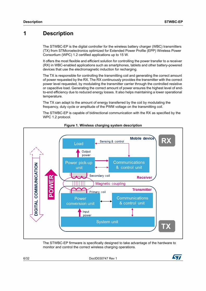
The STWBC-EP is the digital controller for the wireless battery charger (WBC) transmitters (TX) from STMicroelectronics optimized for Extended Power Profile (EPP) Wireless Power Consortium (WPC) 1.2 certified applications up to 15 W.
It offers the most flexible and efficient solution for controlling the power transfer to a receiver (RX) in WBC-enabled applications such as smartphones, tablets and other battery-powered devices that use the electromagnetic induction for recharging.
The TX is responsible for controlling the transmitting coil and generating the correct amount of power requested by the RX. The RX continuously provides the transmitter with the correct power level requested, by modulating the transmitter carrier through the controlled resistive or capacitive load. Generating the correct amount of power ensures the highest level of end-to-end efficiency due to reduced energy losses. It also helps maintaining a lower operational temperature.
The TX can adapt to the amount of energy transferred by the coil by modulating the frequency, duty cycle or amplitude of the PWM voltage on the transmitting coil.
The STWBC-EP is capable of bidirectional communication with the RX as specified by the WPC 1.2 protocol.
Figure 1. Wireless charging system description
The STWBC-EP firmware is specifically designed to take advantage of the hardware to monitor and control the correct wireless charging operations.
DocID030747 Rev 1 7/32
STWBC-EP STWBC-EP system architecture
32
2 STWBC-EP system architecture
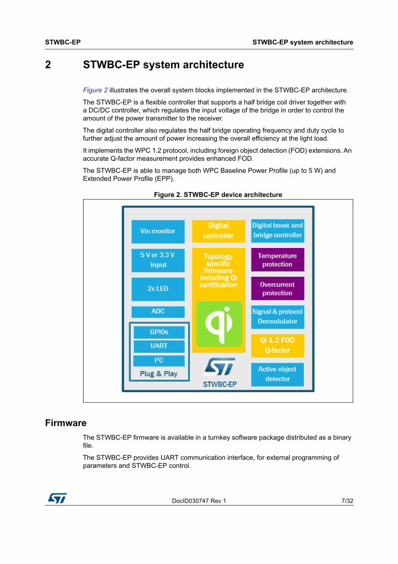
Figure 2 illustrates the overall system blocks implemented in the STWBC-EP architecture.
The STWBC-EP is a flexible controller that supports a half bridge coil driver together with a DC/DC controller, which regulates the input voltage of the bridge in order to control the amount of the power transmitter to the receiver.
The digital controller also regulates the half bridge operating frequency and duty cycle to further adjust the amount of power increasing the overall efficiency at the light load.
It implements the WPC 1.2 protocol, including foreign object detection (FOD) extensions. An accurate Q-factor measurement provides enhanced FOD.
The STWBC-EP is able to manage both WPC Baseline Power Profile (up to 5 W) and Extended Power Profile (EPP).
Figure 2. STWBC-EP device architecture
FirmwareThe STWBC-EP firmware is available in a turnkey software package distributed as a binary file.
The STWBC-EP provides UART communication interface, for external programming of parameters and STWBC-EP control.
Reference design STWBC-EP
8/32 DocID030747 Rev 1
3 Reference design
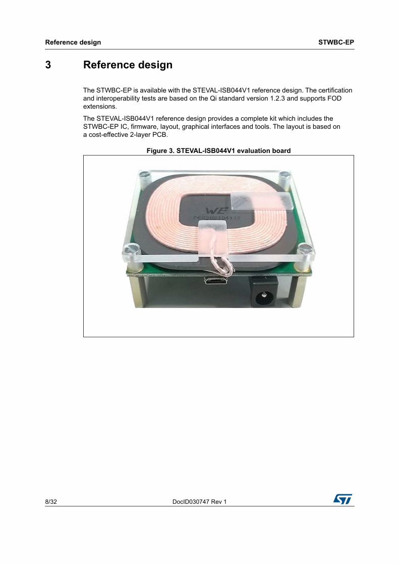
The STWBC-EP is available with the STEVAL-ISB044V1 reference design. The certification and interoperability tests are based on the Qi standard version 1.2.3 and supports FOD extensions.
The STEVAL-ISB044V1 reference design provides a complete kit which includes the STWBC-EP IC, firmware, layout, graphical interfaces and tools. The layout is based on a cost-effective 2-layer PCB.
Figure 3. STEVAL-ISB044V1 evaluation board
DocID030747 Rev 1 9/32
STWBC-EP STWBC-EP pinout and pin description
32
4 STWBC-EP pinout and pin description
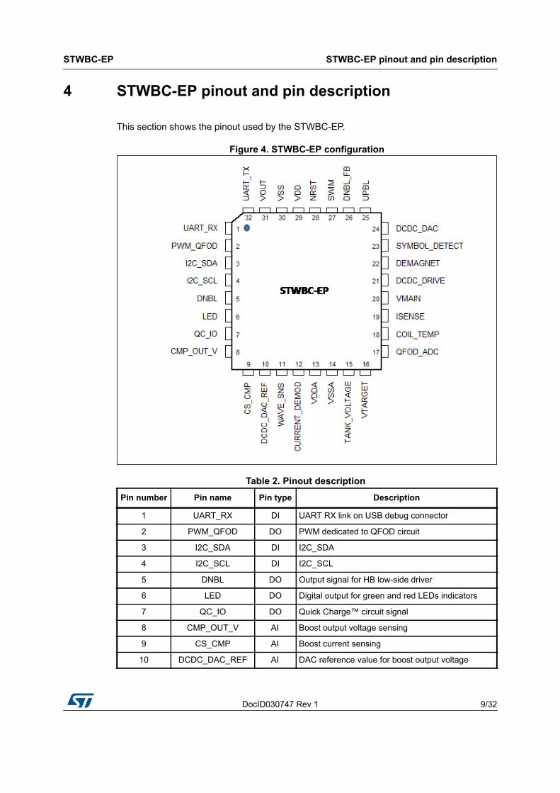
This section shows the pinout used by the STWBC-EP.
Figure 4. STWBC-EP configuration
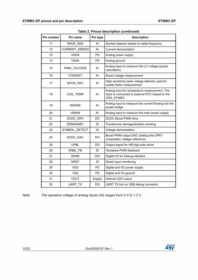
Table 2. Pinout description Pin number Pin name Pin type Description
1 UART_RX DI UART RX link on USB debug connector
2 PWM_QFOD DO PWM dedicated to QFOD circuit
3 I2C_SDA DI I2C_SDA
4 I2C_SCL DI I2C_SCL
5 DNBL DO Output signal for HB low-side driver
6 LED DO Digital output for green and red LEDs indicators
7 QC_IO DO Quick Charge™ circuit signal
8 CMP_OUT_V AI Boost output voltage sensing
9 CS_CMP AI Boost current sensing
10 DCDC_DAC_REF AI DAC reference value for boost output voltage
STWBC-EP pinout and pin description STWBC-EP
10/32 DocID030747 Rev 1
Note: The operative voltage of analog inputs (AI) ranges from 0 V to 1.2 V.
11 WAVE_SNS AI Symbol detector based on delta frequency
12 CURRENT_DEMOD AI Current demodulation
13 VDDA PS Analog power supply
14 VSSA PS Analog ground
15 TANK_VOLTAGE AI Analog input to measure the LC voltage (power calculation)
16 VTARGET AI Boost voltage measurement
17 QFOD_ADC AI High sensitivity peak voltage detector used for quality factor measurement
18 COIL_TEMP AIAnalog input for temperature measurement. The input is connected to external NTC biased to the VDD_STWBC
19 ISENSE AI Analog input to measure the current flowing into the power bridge
20 VMAIN AI Analog input to measure the main power supply
21 DCDC_DRV DO DCDC Boost PWM drive
22 DEMAGNET DI Transformer demagnetization sensing
23 SYMBOL_DETECT DI Voltage demodulation
24 DCDC_DAC DO Boost PWM output DAC (setting the CPP3 comparator voltage reference)
25 UPBL DO Output signal for HB high-side driver
26 DNBL_FB DI Hardware PWM feedback
27 SWIM DIO Digital I/O for Debug interface
28 NRST DI Reset input monitoring
29 VDD PS Digital and I/O power supply
30 VSS PS Digital and I/O ground
31 VOUT Supply Internal LDO output
32 UART_TX DO UART TX link on USB debug connector
Table 2. Pinout description (continued)Pin number Pin name Pin type Description
DocID030747 Rev 1 11/32
STWBC-EP Pins functional description
32
5 Pins functional description
This section describes the functions related to the pins of the device.
5.1 Power supplies: VDD, VDDA, VSS, VSSA, VOUTThe digital portion of the STWBC-EP is powered using VDD and VSS (typically 4.5 V).
The analog portion of the STWBC-EP is powered using VDDA and VSSA (typically 4.5 V).
VDD and VDDA should be correctly filtered to allow the correct operation of the device.
The STWBC-EP generates its own internal power supply which needs a filter capacitor of 1 μF on the VOUT pin.
5.2 DC/DC converter: DCDC_DRV, DCDC_DAC, CMP_OUT_V, CS_CMP, DCDC_DAC_REF, DEMAGNET, VTARGETThe STWBC-EP is designed to drive a DC/DC boost converter placed in front of the half bridge coil driver. The DC/DC power switch (external NMOS) is driven by the DCDC_DRV pin through an output buffer.
The DC/DC inductor charging current is monitored using a sense resistor. The sense resistor has to be connected to the CS_CMP pin so that the STWBC-EP can detect the current flowing into the inductor.
The DC/DC converter loop compares a reference target voltage applied on the DCDC_DAC_REF pin with the feedback voltage connected to the CMP_OUT_V pin. The CMP_OUT_V signal is a partition of the DC/DC output voltage.
The DCDC_DAC_REF reference voltage is variable in order to adjust the DC/DC output voltage depending on wireless power solution requirements. The DCDC_DAC_REF is generated by filtering the PWM signal present on the DCDC_DAC pin. A second order passive filter is required.
The DC/DC output voltage is monitored by the STWBC-EP using the VTARGET pin. The VTARGET should be generated as a partition of the DCDC output voltage.
In order to enhance the efficiency at the medium and low load, the DC/DC converter can operate in the quasi-resonant mode. To do so, the STWBC-EP monitors the demagnetization of the inductor using the DEMAGNET pin.
Pins functional description STWBC-EP
12/32 DocID030747 Rev 1
5.3 Half bridge driver: UPBL, DNBL, PWM_QFOD, WAVE_SNSThe power half bridge is driven using the UPBL and DNBL pins. The UPBL pin has to be connected to a high-side gate driver, while the DNBL pin has to be connected to a low-side gate driver for the power switches.
The UPBL and DNBL pins are active-high: when 1, the corresponding power switch has to be ON.
The STWBC-EP integrates programmable dead time between the active states of the UPBL and DNBL avoiding simultaneous conduction of power switches. The external gate driver doesn't need to manage dead time.
The STWBC-EP requires the following capability to be supported by the gate driver: UPBL = 0, DNBL = 0: in such case, the power half bridge must be in the high
impedance state. UPBL = 1, DNBL = 0: high-side power switch must be ON. UPBL = 0, DNBL = 1: low-side power switch must be ON. UPBL = 1, DNBL = 1: optional mode where both high and low-side power switches
must be ON (simultaneous conduction).
While the power half bridge is driven with UPBL and DNBL signals, a low energy drive is needed to run the coil quality factor estimation. For this function, the bridge is driven by using the PWM_QFOD pin instead of the UPBL (UPBL is 0 during this operation). The PWM_QFOD has to be connected to the low energy high-side switch while the DNBL is still used for the low-side low impedance switch drive.
In many situation the STWBC-EP requires ¼ wave synchronization with the LC tank connected to the half bridge. A simple passive detector must be connected to the LC tank and the WAVE_SNS pin. The WAVE_SNS pin should be limited to a 0.6 V swing.
5.4 Wireless power functions: TANK_VOLTAGE, ISENSE, COIL_TEMP, SYMBOL_DETECT, CURRENT_DEMOD, CS_CMP_AVGThe STWBC-EP requires monitoring the peak voltage on the LC tank as well as the rectified current circulating in the tank. To do so, a peak voltage detector of the LC tank must be connected to the TANK_VOLTAGE pin and a filtered current sensor must be connected to the ISENSE pin .
For quality factor measurement, a high sensitivity peak voltage detector of the LC tank must be connected to the CS_CMP_AVG pin.
The STWBC-EP requires external signal conditioning blocks to pre-demodulate the WPC Qi messages. One of this blocks detects the effect of modulation on the LC tank voltage and it must be connected to the SYMBOL_DETECT pin. Another block is required to detect the effect of modulation on the LC tank current and it must be connected to the CURRENT_DEMOD pin.
For safety reason the STWBC is capable of monitoring the temperature of the transmitting coil. In order to do so, a NTC thermistor must be connected to the COIL_TEMP pin.
DocID030747 Rev 1 13/32
STWBC-EP Pins functional description
32
5.5 Input power supply management: VMAIN, QC_IOThe STWBC-EP monitors the input power supply voltage using the VMAIN pin. This voltage is used for optimum programming of the DC-DC converter but also for the wireless power mode of the operation.
The STWBC-EP is capable of requesting 12 V output voltage available from some USB wall adaptors. While the USB wall adaptor provides 5 V by default, using a specific signaling on the D+ and D- signals of the USB interface, 12 V can be obtained if supported. When 12 V is available, the STWBC-EP can provide up to 15 W to a receiver load. The QC_IO pin has to be connected to a simple interfacing circuit with the USB connector. When QC_IO is 0, 5 V is requested to the USB wall adaptor. When QC_IO is 1, 12 V is requested to the USB wall adaptor.
5.6 External digital interface: UART_TX, UART_RXThe STWBC-EP can be programmed and/or controlled using a 57600 bps 8-bit 1start 1stop no-parity UART interface. The STWBC-EP UART TX output is present on the UART_TX pin and the UART RX input is present on the UART_RX pin.
5.7 End user signaling: LEDThe STWBC-EP manages 2 LEDs (red and green typically) using a single LED pin. The pin is the output 0 to drive the first LED, the output 1 to drive the second LED and high impedance to not drive any LED. A simple circuit can be used to interface the LEDs with this LED pin.
5.8 Expansion interface: I2C_SDA, I2C_SCLThe STWBC-EP embeds an I²C master interface on the I2C_SDA and I2C_SCL pins. This interface is typically inactive and reserved for future use.
5.9 Debug: SWIM, NRSTThe SWIM pin may be used to interface with the STLINK/V2 debugger. The STWBC-EP can be reset using the active-low NRST pin.
Electrical characteristics STWBC-EP
14/32 DocID030747 Rev 1
6 Electrical characteristics
6.1 Parameter conditionsUnless otherwise specified, all voltages are referred to VSS. VDDA and VDD must be connected to the same voltage value. VSS and VSSA must be connected to together with the shortest wire loop.
6.2 Minimum and maximum valuesUnless otherwise specified, the minimum and maximum values are guaranteed in the worst conditions of ambient temperature, supply voltage and frequencies by tests in production on 100% of the devices with the ambient temperature at TA = 25 °C and TA = TA max. (given by the selected temperature range).
6.3 Typical valuesUnless otherwise specified, typical data are based on TA = 25 °C, VDD and VDDA = 5 V. They are given only as design guidelines and are not tested. Typical ADC accuracy values are determined by characterization of a batch of samples from a standard diffusion lot over the full temperature range.
6.4 Typical curvesUnless otherwise specified, all typical curves are given as design guidelines only and are not tested.
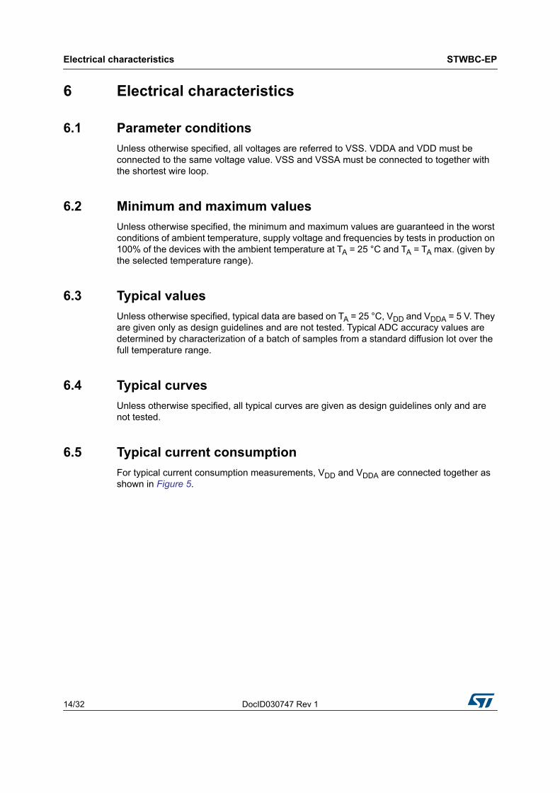
6.5 Typical current consumptionFor typical current consumption measurements, VDD and VDDA are connected together as shown in Figure 5.
DocID030747 Rev 1 15/32
STWBC-EP Electrical characteristics
32
Figure 5. Supply current measurement conditions
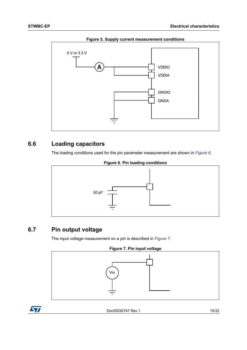
6.6 Loading capacitorsThe loading conditions used for the pin parameter measurement are shown in Figure 6.
Figure 6. Pin loading conditions
6.7 Pin output voltageThe input voltage measurement on a pin is described in Figure 7.
Figure 7. Pin input voltage
Electrical characteristics STWBC-EP
16/32 DocID030747 Rev 1
6.8 Absolute maximum ratingsStresses above those listed as “absolute maximum ratings” may cause permanent damage to the device. This is a stress rating only and the functional operation of the device under these conditions is not implied. Exposure to maximum rating conditions for extended periods may affect the device reliability.
Table 3. Voltage characteristicsSymbol Ratings Min. Max. Unit
VDDX - VSSX Supply voltage(1)
1. All power VDDX (VDD, VDDA) and ground VSSX (VSS, VSSA) pins must always be connected to the external power supply.
-0.3 6.5V
VIN Input voltage on any other pin(2)
2. IINJ(PIN) must never be exceeded. This is implicitly insured if VIN maximum is respected. If VIN maximum cannot be respected, the injection current must be limited externally to the IINJ(PIN) value. A positive injection is induced by VIN > VDD while a negative injection is induced by VIN < VSS.
VSS -0.3 VDD +0.3
VDD - VDDA Variation between different power pins - 50 mV
VSS - VSSA Variation between all the different ground pins(3)
3. VSS and VSSA signals must be interconnected together with a short wire loop.
- 50 mV
Table 4. Current characteristicsSymbol Ratings Max.(1)
1. Data based on characterization results, not tested in production.
Unit
IVDDX Total current into VDDX power lines(2)
2. All power VDDX (VDD, VDDA) and ground VSSX (VSS, VSSA) pins must always be connected to the external power supply.
100
mA
IVSSX Total current out of VSSX power lines(2) 100
IIOOutput current sunk by any I/Os and control pin Ref. to Table 10 on
page 21
Output current source by any I/Os and control pin -
IINJ(PIN)(3), (4)
3. IINJ(PIN) must never be exceeded. This is implicitly insured if VIN maximum is respected. If VIN maximum cannot be respected, the injection current must be limited externally to the IINJ(PIN) value. A positive injection is induced by VIN > VDD while a negative injection is induced by VIN < VSS.
4. Negative injection disturbs the analog performance of the device.
Injected current on any pin ±4
IINJ(TOT) (3),(4), (5)
5. When several inputs are submitted to a current injection, the maximum IINJ(PIN) is the absolute sum of the positive and negative injected currents (instantaneous values). These results are based on characterization with IINJ(PIN) maximum current injection on four I/O port pins of the device.
Sum of injected currents ±20
Table 5. Thermal characteristicsSymbol Ratings Max. Unit
TSTG Storage temperature range -65 to 150ºC
TJ Maximum junction temperature 150
DocID030747 Rev 1 17/32
STWBC-EP Electrical characteristics
32
6.9 Operating conditionsThe device must be used in operating conditions that comply with the parameters in Table 6. In addition, a full account must be taken for all physical capacitor characteristics and tolerances.
Table 6. General operating conditionsSymbol Parameter Conditions Min. Typ. Max. Unit
fCPU Internal CPU clock frequency - - 16 - MHz
VDD1, VDDA1 Operating voltages - 3(1)
1. The external power supply can range from 3 V to 5.5 V although IC performances are optimized for power supply equal to 5 V.
5 5.5(1)
VVDD, VDDA Nominal operating voltages - 3.3(1) 5 5(1)
VOUT
Core digital power supply - - 1.8(2)
2. Internal core power supply voltage.
-
CVOUT: capacitance of external capacitor(3)
3. Care should be taken when the capacitor is selected due to its tolerance, its dependency on temperature, DC bias and frequency.
at 1 MHz 470 - 3300 nF
ESR of external capacitor - 0.05 - 0.2
ESL of external capacitor - - - 15 nH
JA(4)
4. To calculate PDmax (TA), use the formula PDmax = (TJmax - TA)/JA.
FR4 multilayer PCB VFQFPN32 - 26 - °C/W
TA Ambient temperature Pd = 100 mW -40 - 105 °C
Table 7. Operating conditions at power-up/power-downSymbol Parameter Conditions Min Typ. Max Unit
VIT+ Power-on reset threshold - 2.65 2.8 2.98(1)
1. VDD rise must be monotone. The slew rate should be between 1 V/s to 0.5 V/s.
VVIT- Brownout reset threshold - 2.58 2.73 2.88(1)
VHYS(BOR) Brownout reset hysteresis - - 70 - mV
Electrical characteristics STWBC-EP
18/32 DocID030747 Rev 1
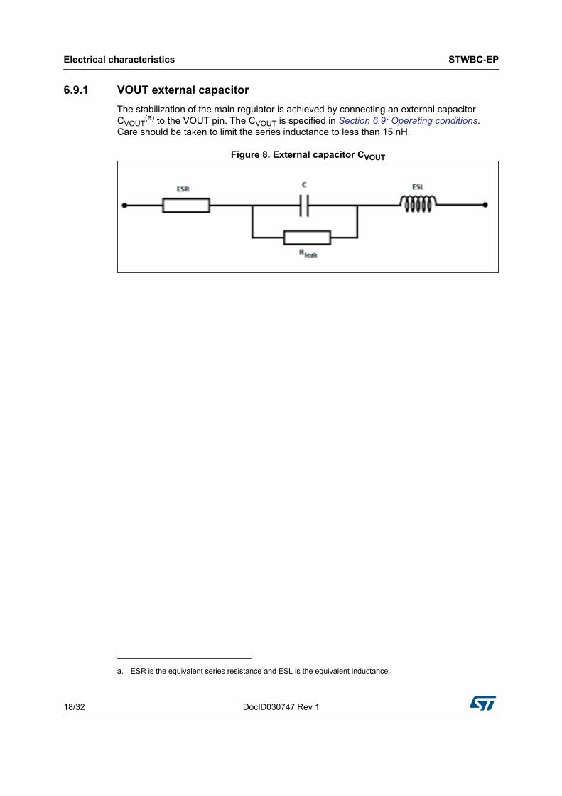
6.9.1 VOUT external capacitorThe stabilization of the main regulator is achieved by connecting an external capacitor CVOUT
(a) to the VOUT pin. The CVOUT is specified in Section 6.9: Operating conditions. Care should be taken to limit the series inductance to less than 15 nH.
Figure 8. External capacitor CVOUT
a. ESR is the equivalent series resistance and ESL is the equivalent inductance.
DocID030747 Rev 1 19/32
STWBC-EP Electrical characteristics
32
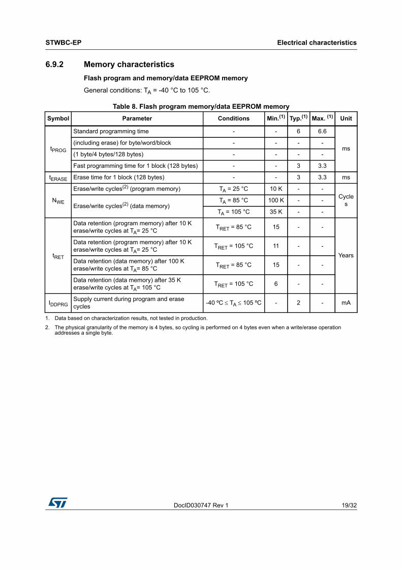
6.9.2 Memory characteristicsFlash program and memory/data EEPROM memory
General conditions: TA = -40 °C to 105 °C.
Table 8. Flash program memory/data EEPROM memorySymbol Parameter Conditions Min.(1) Typ.(1) Max. (1) Unit
tPROG
Standard programming time - - 6 6.6
ms(including erase) for byte/word/block - - - -
(1 byte/4 bytes/128 bytes) - - - -
Fast programming time for 1 block (128 bytes) - - 3 3.3
tERASE Erase time for 1 block (128 bytes) - - 3 3.3 ms
NWE
Erase/write cycles(2) (program memory) TA = 25 °C 10 K - -Cycle
sErase/write cycles(2) (data memory)TA = 85 °C 100 K - -
TA = 105 °C 35 K - -
tRET
Data retention (program memory) after 10 K erase/write cycles at TA= 25 °C TRET = 85 °C 15 - -
Years
Data retention (program memory) after 10 K erase/write cycles at TA= 25 °C TRET = 105 °C 11 - -
Data retention (data memory) after 100 K erase/write cycles at TA= 85 °C TRET = 85 °C 15 - -
Data retention (data memory) after 35 K erase/write cycles at TA= 105 °C TRET = 105 °C 6 - -
IDDPRGSupply current during program and erase cycles -40 ºC TA 105 ºC - 2 - mA
1. Data based on characterization results, not tested in production.
2. The physical granularity of the memory is 4 bytes, so cycling is performed on 4 bytes even when a write/erase operation addresses a single byte.
Electrical characteristics STWBC-EP
20/32 DocID030747 Rev 1
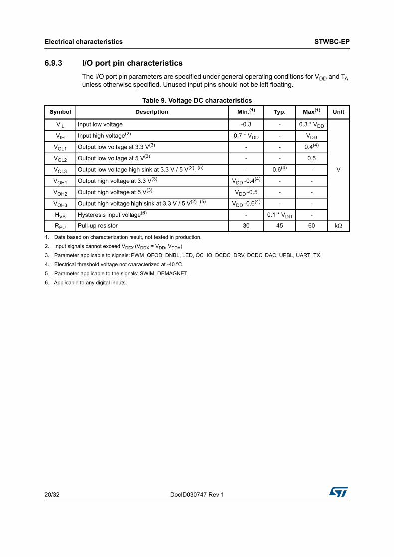
6.9.3 I/O port pin characteristicsThe I/O port pin parameters are specified under general operating conditions for VDD and TA unless otherwise specified. Unused input pins should not be left floating.
Table 9. Voltage DC characteristicsSymbol Description Min.(1) Typ. Max(1) Unit
VIL Input low voltage -0.3 - 0.3 * VDD
V
VIH Input high voltage(2) 0.7 * VDD - VDD
VOL1 Output low voltage at 3.3 V(3) - - 0.4(4)
VOL2 Output low voltage at 5 V(3) - - 0.5
VOL3 Output low voltage high sink at 3.3 V / 5 V(2), (5) - 0.6(4) -
VOH1 Output high voltage at 3.3 V(3) VDD -0.4(4) - -
VOH2 Output high voltage at 5 V(3) VDD -0.5 - -
VOH3 Output high voltage high sink at 3.3 V / 5 V(2) ,(5) VDD -0.6(4) - -
HVS Hysteresis input voltage(6) - 0.1 * VDD -
RPU Pull-up resistor 30 45 60 k
1. Data based on characterization result, not tested in production.
2. Input signals cannot exceed VDDX (VDDX = VDD, VDDA).
3. Parameter applicable to signals: PWM_QFOD, DNBL, LED, QC_IO, DCDC_DRV, DCDC_DAC, UPBL, UART_TX.
4. Electrical threshold voltage not characterized at -40 ºC.
5. Parameter applicable to the signals: SWIM, DEMAGNET.
6. Applicable to any digital inputs.
DocID030747 Rev 1 21/32
STWBC-EP Electrical characteristics
32
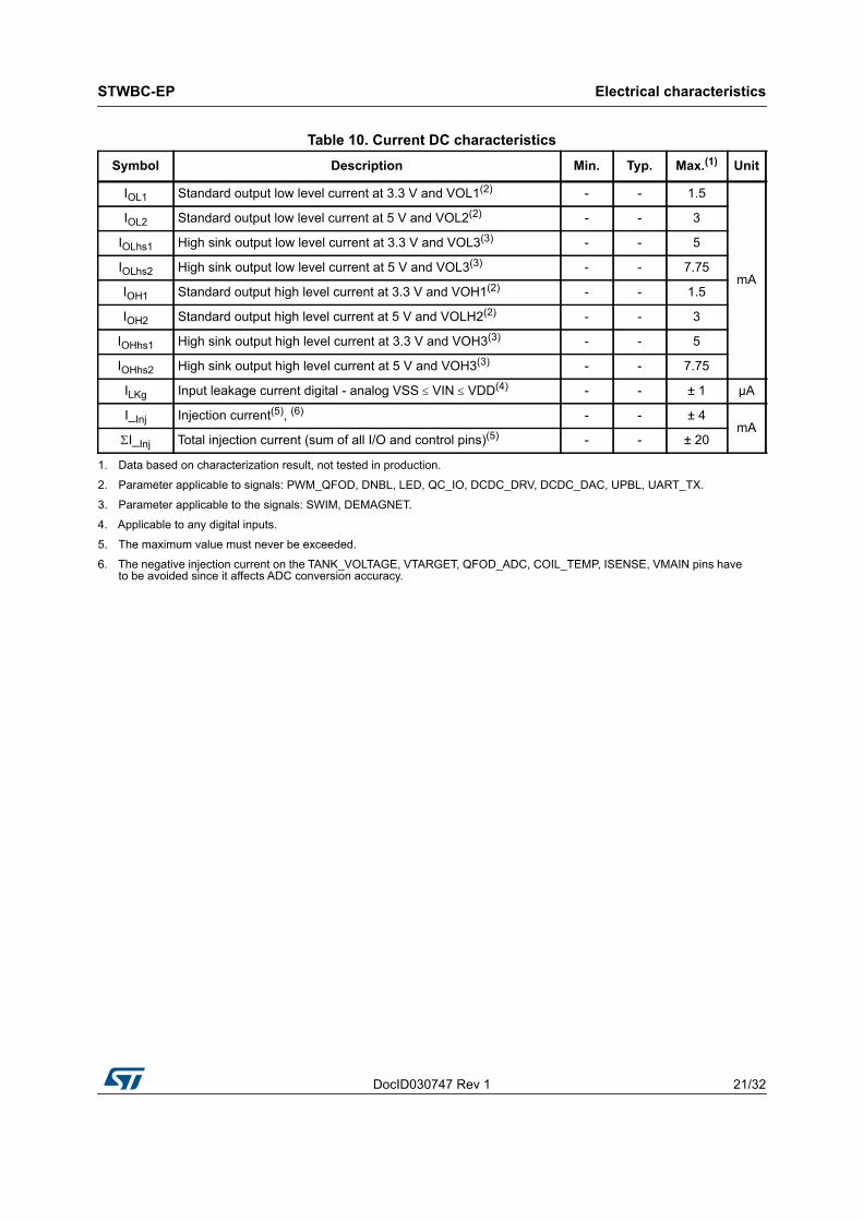
Table 10. Current DC characteristicsSymbol Description Min. Typ. Max.(1) Unit
IOL1 Standard output low level current at 3.3 V and VOL1(2) - - 1.5
mA
IOL2 Standard output low level current at 5 V and VOL2(2) - - 3
IOLhs1 High sink output low level current at 3.3 V and VOL3(3) - - 5
IOLhs2 High sink output low level current at 5 V and VOL3(3) - - 7.75
IOH1 Standard output high level current at 3.3 V and VOH1(2) - - 1.5
IOH2 Standard output high level current at 5 V and VOLH2(2) - - 3
IOHhs1 High sink output high level current at 3.3 V and VOH3(3) - - 5
IOHhs2 High sink output high level current at 5 V and VOH3(3) - - 7.75
ILKg Input leakage current digital - analog VSS VIN VDD(4) - - ± 1 μA
I_Inj Injection current(5), (6) - - ± 4mA
I_Inj Total injection current (sum of all I/O and control pins)(5) - - ± 20
1. Data based on characterization result, not tested in production.
2. Parameter applicable to signals: PWM_QFOD, DNBL, LED, QC_IO, DCDC_DRV, DCDC_DAC, UPBL, UART_TX.
3. Parameter applicable to the signals: SWIM, DEMAGNET.
4. Applicable to any digital inputs.
5. The maximum value must never be exceeded.
6. The negative injection current on the TANK_VOLTAGE, VTARGET, QFOD_ADC, COIL_TEMP, ISENSE, VMAIN pins have to be avoided since it affects ADC conversion accuracy.
Electrical characteristics STWBC-EP
22/32 DocID030747 Rev 1
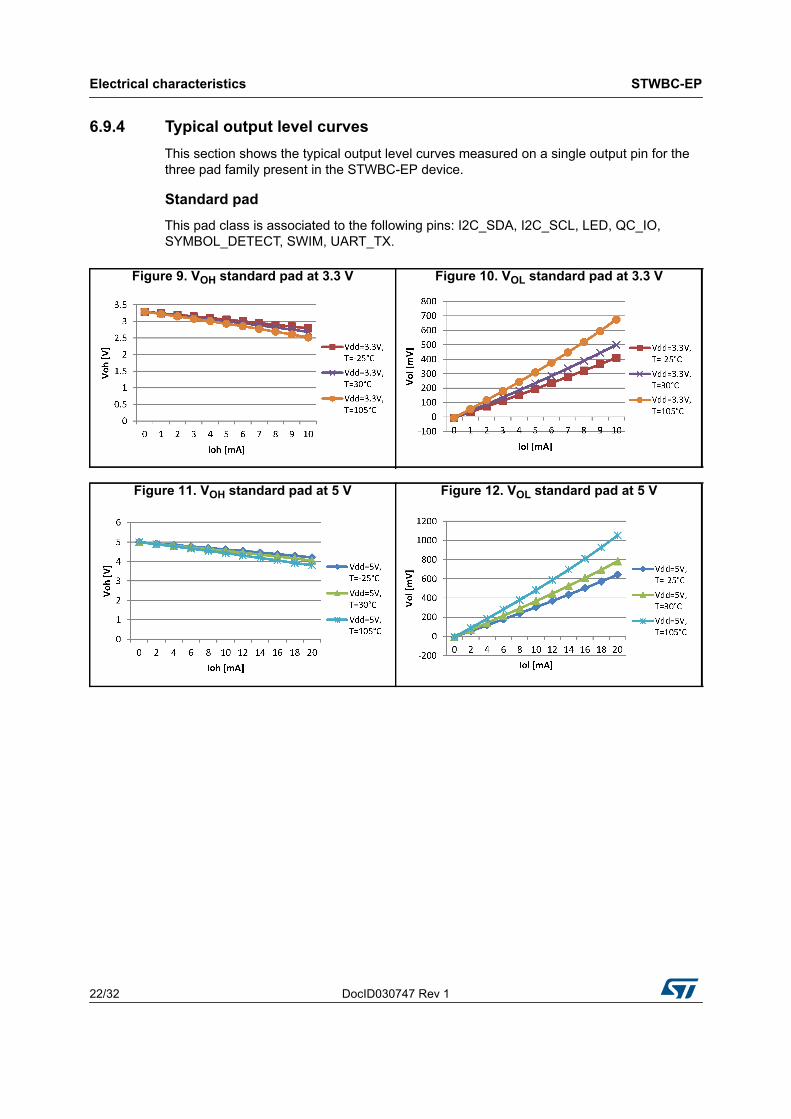
6.9.4 Typical output level curvesThis section shows the typical output level curves measured on a single output pin for the three pad family present in the STWBC-EP device.
Standard pad
This pad class is associated to the following pins: I2C_SDA, I2C_SCL, LED, QC_IO, SYMBOL_DETECT, SWIM, UART_TX.
Figure 9. VOH standard pad at 3.3 V Figure 10. VOL standard pad at 3.3 V
Figure 11. VOH standard pad at 5 V Figure 12. VOL standard pad at 5 V
DocID030747 Rev 1 23/32
STWBC-EP Electrical characteristics
32
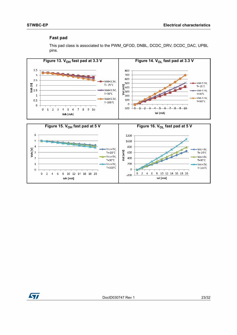
Fast pad
This pad class is associated to the PWM_QFOD, DNBL, DCDC_DRV, DCDC_DAC, UPBL pins.
Figure 13. VOH fast pad at 3.3 V Figure 14. VOL fast pad at 3.3 V
Figure 15. VOH fast pad at 5 V Figure 16. VOL fast pad at 5 V
Electrical characteristics STWBC-EP
24/32 DocID030747 Rev 1
6.9.5 Reset pin characteristicsThe following data are specified under general operating conditions for VDD and TA defined in Table 6 on page 17 unless otherwise specified.
6.9.6 I2C interface characteristics
Table 11. NRST pin characteristicsSymbol Parameter Conditions Min.(1)
1. Data based on characterization results, not tested in production.
Typ. Max.(1) Unit
VIL(NRST) NRST input low level voltage(1) - -0.3 - 0.3 x VDD
VVIH(NRST) NRST input high level voltage(1) - 0.7 x VDD - VDD + 0.3
VOL(NRST) NRST output low level voltage(1) IOL = 2 mA - - 0.5
RPU(NRST) NRST pull-up resistor(2)
2. The RPU pull-up equivalent resistor is based on a resistive transistor.
- 30 40 60 k
tIFP(NRST) NRST input filtered pulse(3)
3. Data guaranteed by design, not tested in production.
- - 75ns
tINFP(NRST) NRST not input filtered pulse(3) - 500 - -
tOP(NRST) NRST output filtered pulse(3) - 15 - - μs
Table 12. I2C interface characteristics
Symbol ParameterStandard mode Fast mode
UnitMin.(1)
1. Data based on the standard I2C protocol requirement, not tested in production.
Max.(1) Min.(1) Max.(1)
tw(SCLL) SCL clock low time 4.7 - 1.3 -μs
tw(SCLH) SCL clock high time 4.0 - 0.6 -
tsu(SDA) SDA setup time 250 - 100 -
nsth(SDA) SDA data hold time 0(2)
2. The maximum hold time of the start condition has only to be met if the interface does not stretch the low time.
- 0(2) 900(2)
tr(SDA) tr(SCL) SDA and SCL rise time (VDD = 3.3 to 5 V)(3)
3. I2C multifunction signals require the high sink pad configuration and the interconnection of 1 k pull-up resistances.
- 1000 - 300
tf(SDA) tf(SCL) SDA and SCL fall time (VDD = 3.3 to 5 V)(3) - 300 - 300
th(STA) START condition hold time 4.0 - 0.6 -μs
tsu(STA) Repeated START condition setup time 4.7 - 0.6 -
tsu(STO) STOP condition setup time 4.0 - 0.6 - μs
tw(STO:STA) STOP to START condition time (bus free) 4.7 - 1.3 - μs
Cb Capacitive load for each bus line(4)
4. 50 pF is the maximum load capacitance value to meet the I2C std. timing specifications.
- 50 - 50 pF
DocID030747 Rev 1 25/32
STWBC-EP Electrical characteristics
32
6.9.7 10-bit SAR ADC characteristicsThe 10-bit SAR ADC parameters are specified under general operating conditions for VDDA and TA unless otherwise specified.
ADC accuracy characteristics
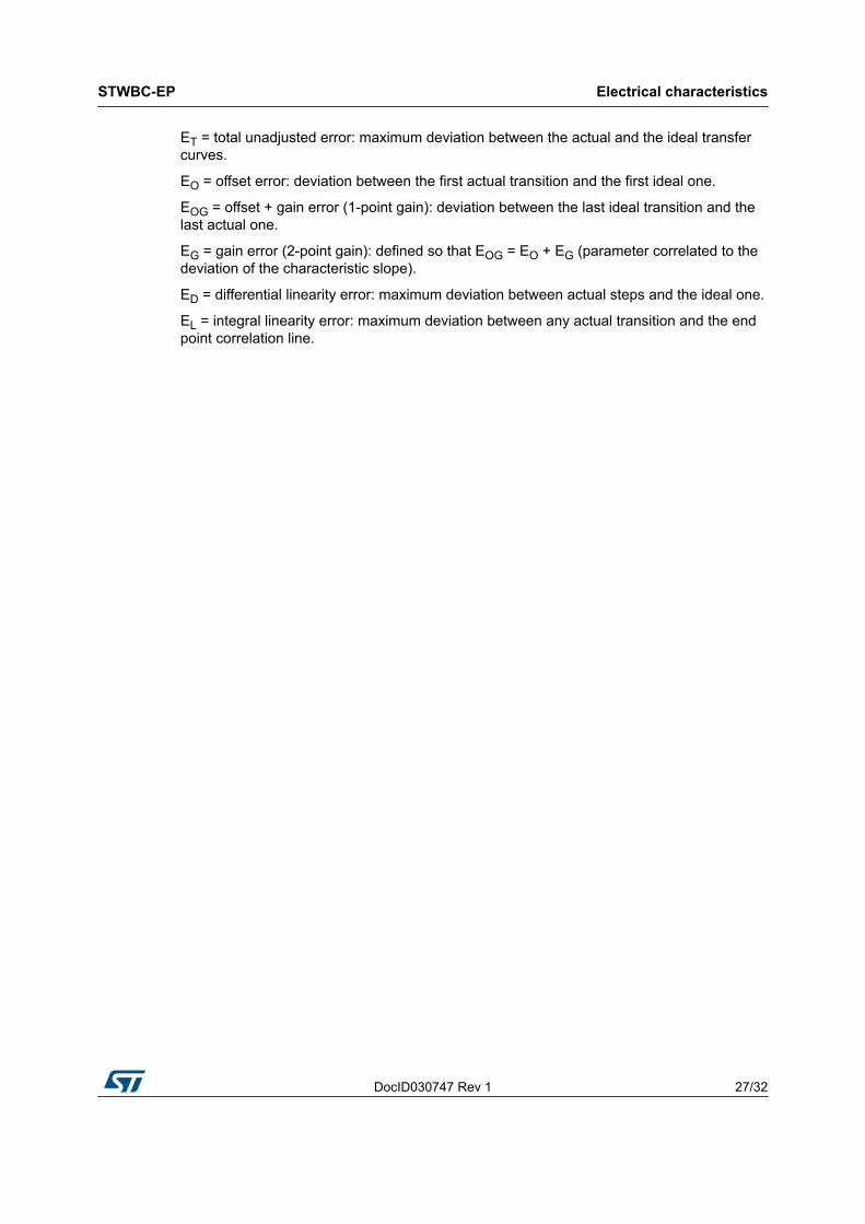
See Figure 18 for more details about the ADC accuracy parameter definition.
Table 13. ADC characteristicsSymbol Parameter Min. Typ. Max. Unit
N Resolution - 10 - bit
RADCIN ADC input impedance(1)
1. Maximum input analog voltage cannot exceed VDD/VDDA.
1 - - M
VIN Input conversion voltage range 0 - 1.25(1),(2)
2. Exceeding the maximum voltage on the TANK_VOLTAGE, VTARGET, COIL_TEMP, ISENSE, QFOD_ADC signals has to be avoided since it may impact the ADC conversion accuracy defined in Table 14.
VVref ADC main reference voltage(3)
3. ADC reference voltage at TA = 25 °C.
- 1.250 -
Table 14. ADC accuracy characteristic at VDD/VDDA = 5 VSymbol Parameter Min.(1)
1. Data based on characterization results, not tested in production.
Typ.(2)
2. Operating temperature: TA = 25 °C.
Max.(1) Unit
|EO| Offset error(3), (4)
3. ADC accuracy vs. negative injection current. The injecting negative current on any of the analog input pins should be avoided as this reduces the accuracy of the conversion being performed on another analog input. It is recommended that a Schottky diode (pin to ground) has to be added to standard analog pins which may potentially inject a negative current. Any positive injection current within the limits specified for IINJ(PIN) and IINJ(PIN) in the I/O port pin characteristics section does not affect the ADC accuracy. The ADC accuracy parameters may be also impacted exceeding the ADC maximum input voltage VIN.
4. Results in manufacturing test mode.
- 0.5 -
LSB
|EG| Gain error(3), (4), (5)
5. Gain error evaluated with the two-point method.
- 0.4 -
EOG Offset + Gain error (5), (6)
6. Temperature operating range: 0 ºC TA 85 ºC.
-8.3 - 8.9
EOG Offset + Gain error(5), (7)
7. Temperature operating range: -25 ºC TA 105 ºC.
-10.9 - 10.9
EOG Offset + Gain error(5), (8)
8. Temperature operating range: -40 ºC TA 105 ºC.
-13.8 - 10.9
|ED| Differential linearity error(1), (2), (3) - 0.8 -
|EL| Integral linearity error(3), (4) - 2.0 -
Electrical characteristics STWBC-EP
26/32 DocID030747 Rev 1
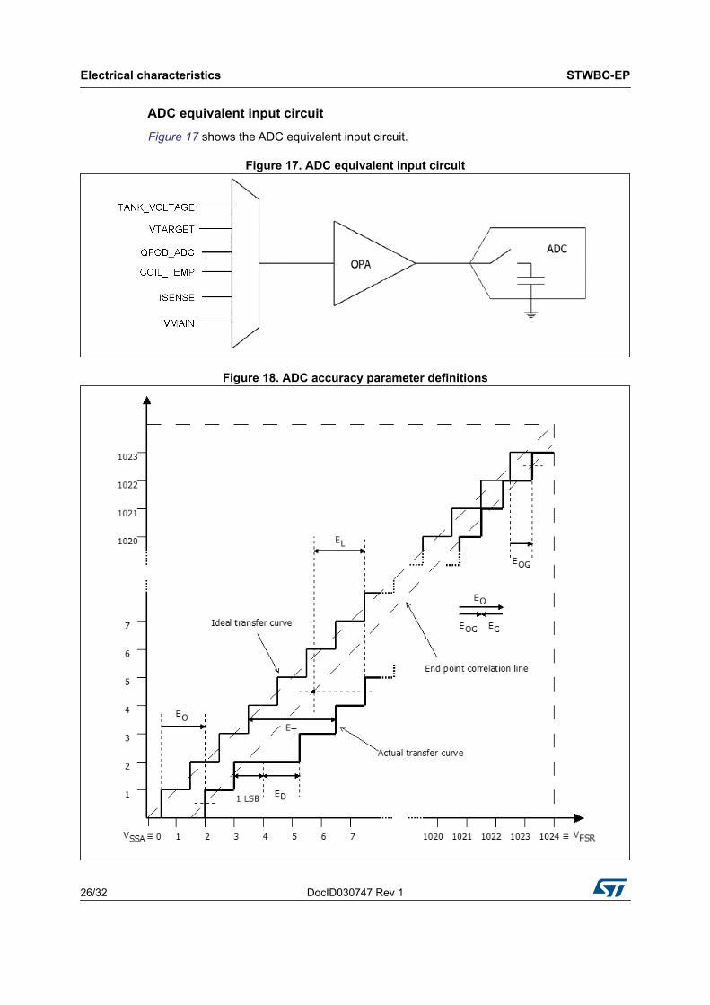
ADC equivalent input circuit
Figure 17 shows the ADC equivalent input circuit.
Figure 17. ADC equivalent input circuit
Figure 18. ADC accuracy parameter definitions
DocID030747 Rev 1 27/32
STWBC-EP Electrical characteristics
32
ET = total unadjusted error: maximum deviation between the actual and the ideal transfer curves.
EO = offset error: deviation between the first actual transition and the first ideal one.
EOG = offset + gain error (1-point gain): deviation between the last ideal transition and the last actual one.
EG = gain error (2-point gain): defined so that EOG = EO + EG (parameter correlated to the deviation of the characteristic slope).
ED = differential linearity error: maximum deviation between actual steps and the ideal one.
EL = integral linearity error: maximum deviation between any actual transition and the end point correlation line.
Thermal characteristics STWBC-EP
28/32 DocID030747 Rev 1
7 Thermal characteristics
The STWBC-EP functionality cannot be guaranteed when the device is operating under the maximum chip junction temperature (TJmax).
TJmax, in degrees Celsius, may be calculated using the following equation:
TJmax = TAmax + (PDmax x JA)
where:
TAmax is the maximum ambient temperature in °C.
ΘJA is the package junction to ambient thermal resistance in °C/W.
PDmax is the sum of PINTmax and PI/Omax (PDmax = PINTmax + PI/Omax).
PINTmax is the product of IDD and VDD, expressed in Watts. This is the maximum chip internal power.
PI/Omax represents the maximum power dissipation on output pins where: PI/Omax = (VOL * IOL) + [(VDD - VOH) * IOH], taking into account the actual VOL/IOL and VOH/IOH of the I/Os at the low and high level.
Table 15. Thermal characteristicsSymbol Parameter Value Unit
JA Thermal resistance junction ambient(1)
1. Thermal resistances are based on JEDEC JESD51-2 with the 4-layer PCB in a natural convection environment.
26 °C/W
DocID030747 Rev 1 29/32
STWBC-EP Package information
32
8 Package information
In order to meet environmental requirements, ST offers these devices in different grades of ECOPACK® packages, depending on their level of environmental compliance. ECOPACK specifications, grade definitions and product status are available at: www.st.com. ECOPACK is an ST trademark.
8.1 VFQFPN32 package information
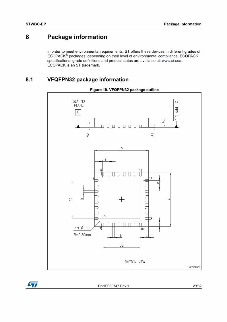
Figure 19. VFQFPN32 package outline
Package information STWBC-EP
30/32 DocID030747 Rev 1
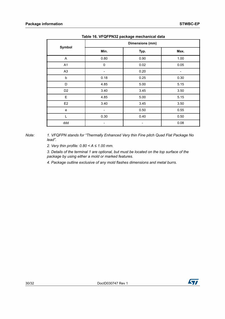
Note: 1. VFQFPN stands for “Thermally Enhanced Very thin Fine pitch Quad Flat Package No lead”.2. Very thin profile: 0.80 < A ≤ 1.00 mm.3. Details of the terminal 1 are optional, but must be located on the top surface of the package by using either a mold or marked features.4. Package outline exclusive of any mold flashes dimensions and metal burrs.
Table 16. VFQFPN32 package mechanical data
Symbol Dimensions (mm)
Min. Typ. Max.
A 0.80 0.90 1.00
A1 0 0.02 0.05
A3 - 0.20 -
b 0.18 0.25 0.30
D 4.85 5.00 5.15
D2 3.40 3.45 3.50
E 4.85 5.00 5.15
E2 3.40 3.45 3.50
e - 0.50 0.55
L 0.30 0.40 0.50
ddd - - 0.08
DocID030747 Rev 1 31/32
STWBC-EP Revision history
32
9 Revision history
Table 17. Document revision history Date Revision Changes
10-Oct-2017 1 Initial release.
STWBC-EP
32/32 DocID030747 Rev 1
IMPORTANT NOTICE – PLEASE READ CAREFULLY
STMicroelectronics NV and its subsidiaries (“ST”) reserve the right to make changes, corrections, enhancements, modifications, and improvements to ST products and/or to this document at any time without notice. Purchasers should obtain the latest relevant information on ST products before placing orders. ST products are sold pursuant to ST’s terms and conditions of sale in place at the time of order acknowledgement.
Purchasers are solely responsible for the choice, selection, and use of ST products and ST assumes no liability for application assistance or the design of Purchasers’ products.
No license, express or implied, to any intellectual property right is granted by ST herein.
Resale of ST products with provisions different from the information set forth herein shall void any warranty granted by ST for such product.
ST and the ST logo are trademarks of ST. All other product or service names are the property of their respective owners.
Information in this document supersedes and replaces information previously supplied in any prior versions of this document.
© 2017 STMicroelectronics – All rights reserved