Embed Size (px)
Citation preview
Digital Microelectronic Circuits The VLSI Systems Center - BGU Lecture 7: Logical Effort 1
Digital Microelectronic
Circuits
(361-1-3021 )
Logical Effort
Presented by: Adam Teman
Lecture 7:
Digital Microelectronic Circuits The VLSI Systems Center - BGU Lecture 7: Logical Effort
Last Lectures
The CMOS Inverter
» Delay Calculation
» Driving a Load
CMOS Digital Logic
» Dealing with High Fan-In
2
Digital Microelectronic Circuits The VLSI Systems Center - BGU Lecture 7: Logical Effort
This Lecture
So we learned how to drive a large load with a chain of
inverters.
But what if there is logic to be calculated along the way?
How should we distribute the logic in order to optimally
drive the load?
Can we develop a methodology for designing a logical
network?
3
Digital Microelectronic Circuits The VLSI Systems Center - BGU Lecture 7: Logical Effort
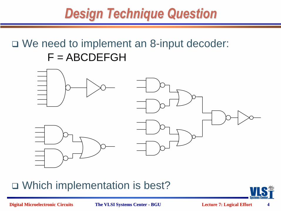
We need to implement an 8-input decoder:
Which implementation is best?
Design Technique Question
4
F = ABCDEFGH
Digital Microelectronic Circuits The VLSI Systems Center - BGU Lecture 7: Logical Effort
5
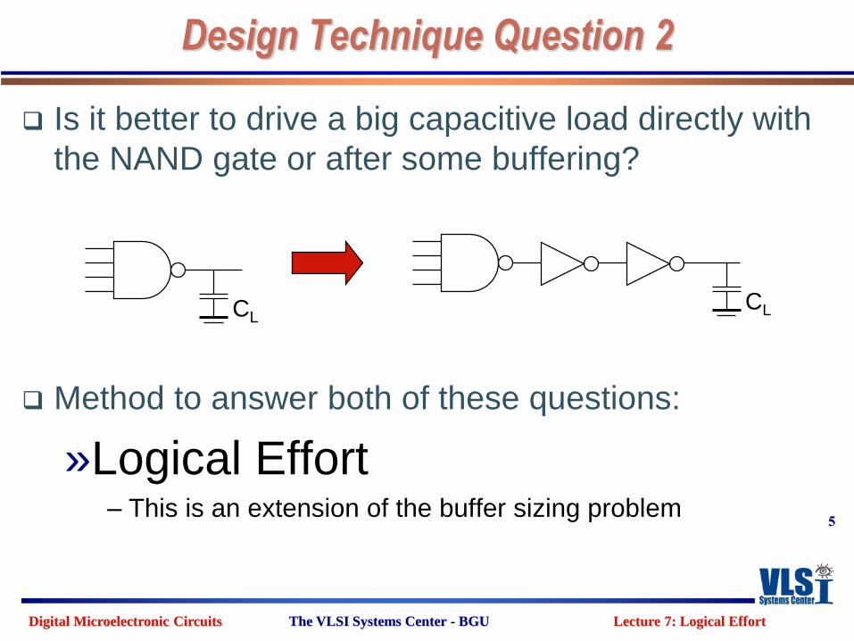
Design Technique Question 2
Is it better to drive a big capacitive load directly with
the NAND gate or after some buffering?
Method to answer both of these questions:
»Logical Effort– This is an extension of the buffer sizing problem
CLCL
Digital Microelectronic Circuits The VLSI Systems Center - BGU Lecture 7: Logical Effort
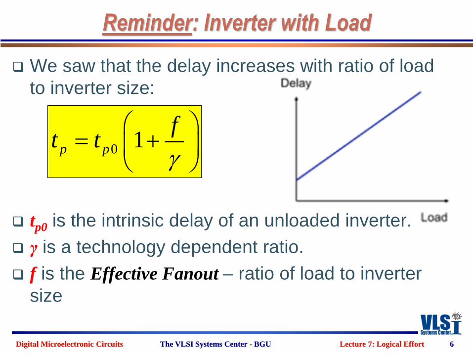
Reminder: Inverter with Load
We saw that the delay increases with ratio of load
to inverter size:
tp0 is the intrinsic delay of an unloaded inverter.
γ is a technology dependent ratio.
f is the Effective Fanout – ratio of load to inverter
size
6
0 1p p
ft t
Digital Microelectronic Circuits The VLSI Systems Center - BGU Lecture 7: Logical Effort
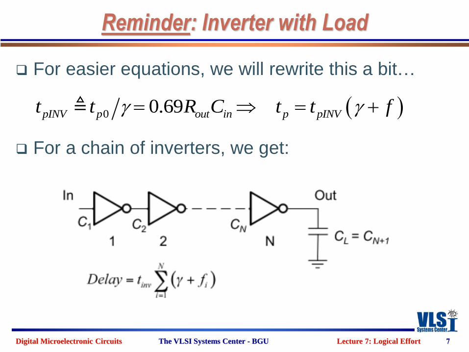
Reminder: Inverter with Load
For easier equations, we will rewrite this a bit…
For a chain of inverters, we get:
7
0 0.69pINV p out in p pINVt t R C t t f
Digital Microelectronic Circuits The VLSI Systems Center - BGU Lecture 7: Logical Effort
An Optimal (reference) Inverter
8
Digital Microelectronic Circuits The VLSI Systems Center - BGU Lecture 7: Logical Effort
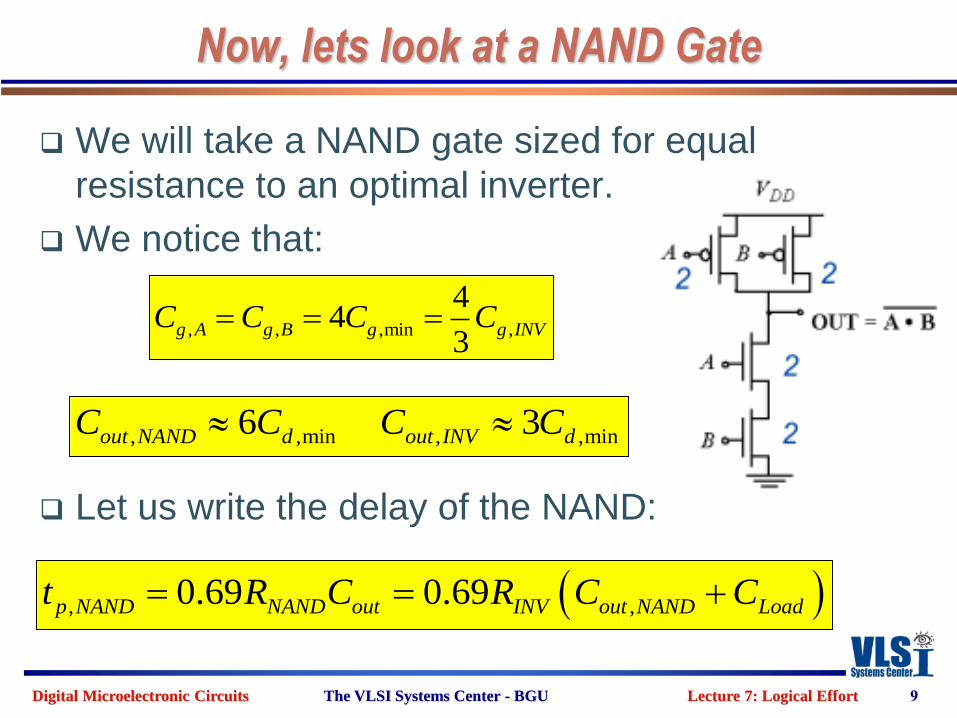
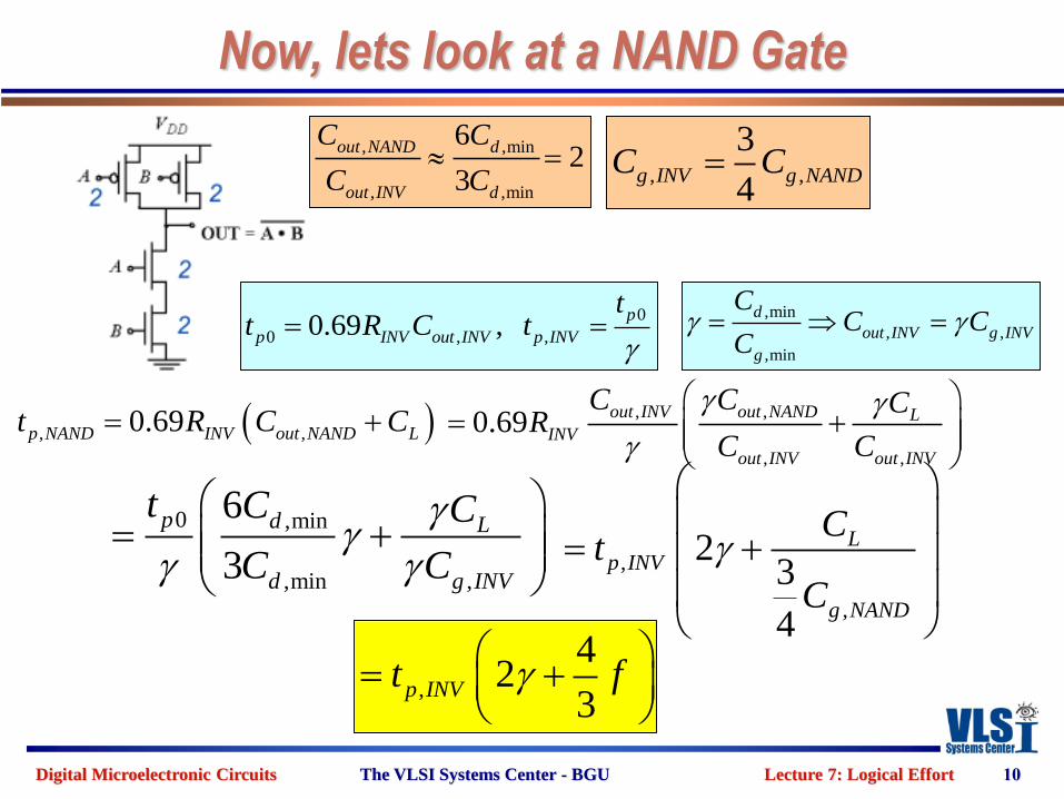
Now, lets look at a NAND Gate
We will take a NAND gate sized for equal
resistance to an optimal inverter.
We notice that:
Let us write the delay of the NAND:
9
, , ,min ,
44
3g A g B g g INVC C C C
, ,min , ,min6 3out NAND d out INV dC C C C
, ,0.69 0.69p NAND NAND out INV out NAND Loadt R C R C C
Digital Microelectronic Circuits The VLSI Systems Center - BGU Lecture 7: Logical Effort
Now, lets look at a NAND Gate
10
, ,
3
4g INV g NANDC C
, ,min
, ,min
62
3
out NAND d
out INV d
C C
C C
, ,0.69p NAND INV out NAND Lt R C C
0
0 , ,0.69 ,p
p INV out INV p INV
tt R C t
,min
, ,
,min
d
out INV g INV
g
CC C
C
, ,
, ,
0.69out INV out NAND L
INV
out INV out INV
C C CR
C C
0 ,min
,min ,
6
3
p d L
d g INV
t C C
C C
,
,
23
4
Lp INV
g NAND
Ct
C
,
42
3p INVt f
Digital Microelectronic Circuits The VLSI Systems Center - BGU Lecture 7: Logical Effort
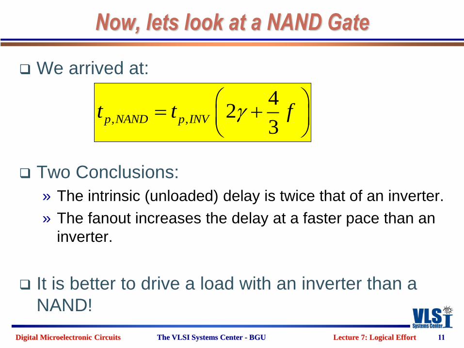
Now, lets look at a NAND Gate
We arrived at:
Two Conclusions:
» The intrinsic (unloaded) delay is twice that of an inverter.
» The fanout increases the delay at a faster pace than an
inverter.
It is better to drive a load with an inverter than a
NAND!
11
, ,
42
3p NAND p INVt t f
Digital Microelectronic Circuits The VLSI Systems Center - BGU Lecture 7: Logical Effort
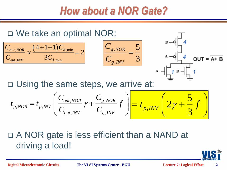
How about a NOR Gate?
We take an optimal NOR:
Using the same steps, we arrive at:
A NOR gate is less efficient than a NAND at
driving a load!
12
,
,
5
3
g NOR
g INV
C
C
, ,min
, ,min
4 1 12
3
out NOR d
out INV d
C C
C C
,,
, ,
, ,
g NORout NOR
p NOR p INV
out INV g INV
CCt t f
C C
,
52
3p INVt f
Digital Microelectronic Circuits The VLSI Systems Center - BGU Lecture 7: Logical Effort
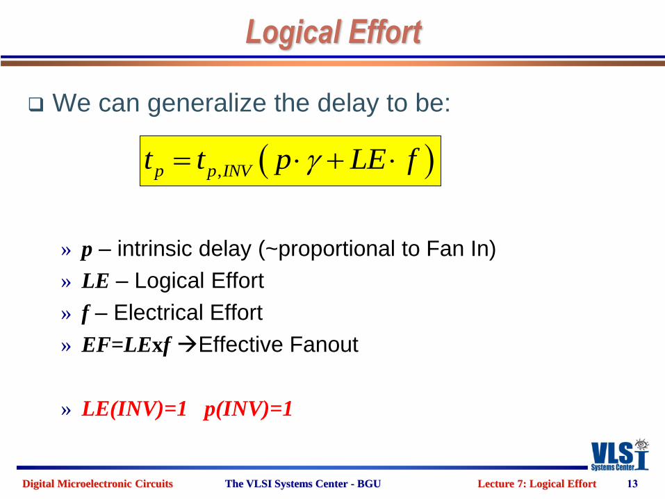
Logical Effort
We can generalize the delay to be:
» p – intrinsic delay (~proportional to Fan In)
» LE – Logical Effort
» f – Electrical Effort
» EF=LExf Effective Fanout
» LE(INV)=1 p(INV)=1
13
,p p INVt t p LE f
Digital Microelectronic Circuits The VLSI Systems Center - BGU Lecture 7: Logical Effort
Logical Effort
To summarize:
» The logical effort of a gate describes how much
“effort” we need to perform a logic calculation.
» An Inverter has the smallest logical effort and
intrinsic delay of all static CMOS gates.
» Logical Effort increases with gate complexity.
14
Digital Microelectronic Circuits The VLSI Systems Center - BGU Lecture 7: Logical Effort
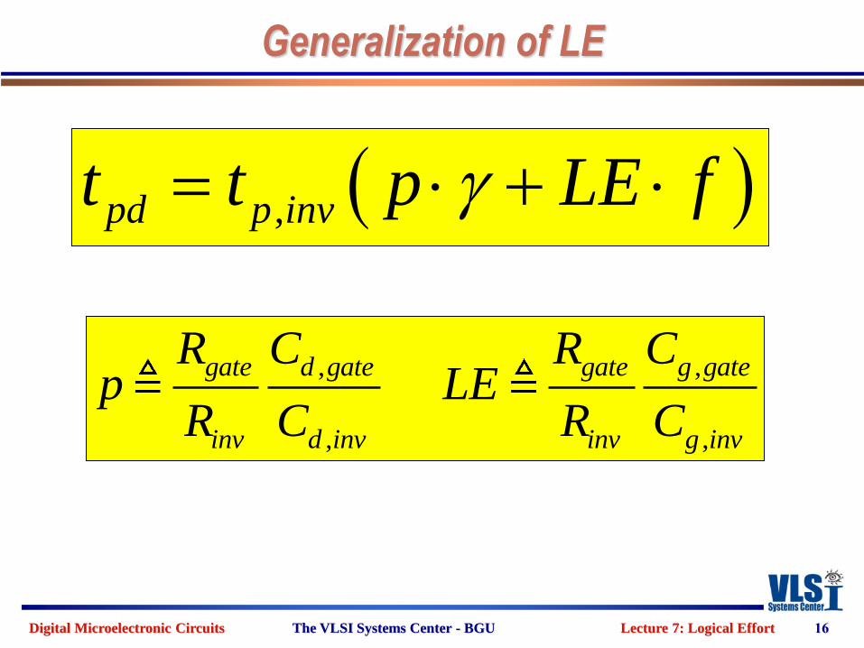
,0.69pd gate d gate Loadt R C C
Generalization of LE
15
,
,
,
0.69d invinv
gate d gate Load
inv d inv
CRR C C
R C
, ,
, ,
gate gate
p inv d gate Load
inv d inv inv d inv
R Rt C C
R C R C
,
,
, ,
1gate g gate
p inv Load
inv g inv g gate
R Ct p C
R C C
,p invt p LE f
,
,
0.69 inv d inv
p inv
R Ct
, ,
,
,
,gate d gate d inv
g inv
inv d inv
R C Cp C
R C
,
, ,
,gate g gate Load
inv g inv g gate
R C CLE f
R C C
Digital Microelectronic Circuits The VLSI Systems Center - BGU Lecture 7: Logical Effort
Generalization of LE
16
, ,
, ,
gate d gate gate g gate
inv d inv inv g inv
R C R Cp LE
R C R C
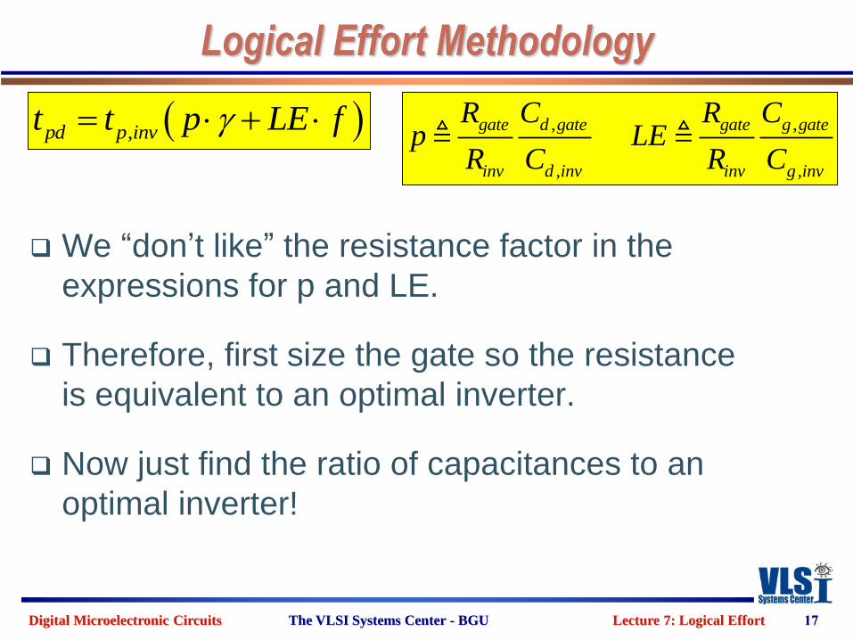
,pd p invt t p LE f
Digital Microelectronic Circuits The VLSI Systems Center - BGU Lecture 7: Logical Effort
Logical Effort Methodology
We “don’t like” the resistance factor in the
expressions for p and LE.
Therefore, first size the gate so the resistance
is equivalent to an optimal inverter.
Now just find the ratio of capacitances to an
optimal inverter!
17
,pd p invt t p LE f , ,
, ,
gate d gate gate g gate
inv d inv inv g inv
R C R Cp LE
R C R C

Digital Microelectronic Circuits The VLSI Systems Center - BGU Lecture 7: Logical Effort
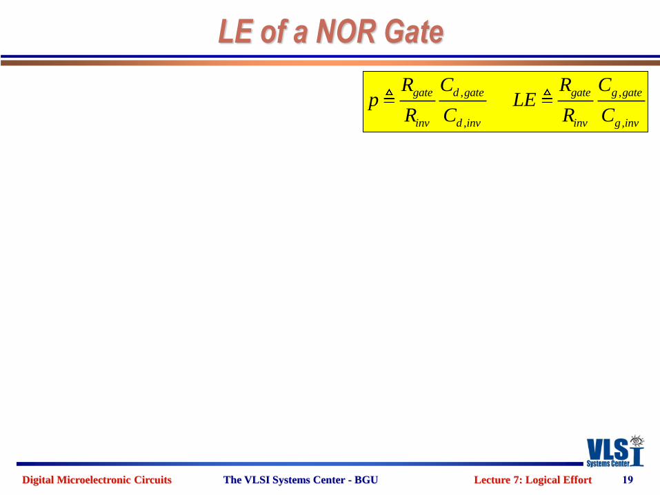
LE of a NAND Gate
18
, ,
, ,
gate d gate gate g gate
inv d inv inv g inv
R C R Cp LE
R C R C
Digital Microelectronic Circuits The VLSI Systems Center - BGU Lecture 7: Logical Effort
LE of a NOR Gate
19
, ,
, ,
gate d gate gate g gate
inv d inv inv g inv
R C R Cp LE
R C R C
Digital Microelectronic Circuits The VLSI Systems Center - BGU Lecture 7: Logical Effort
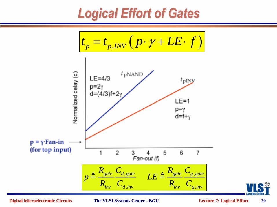
Logical Effort of Gates
20
,p p INVt t p LE f
, ,
, ,
gate d gate gate g gate
inv d inv inv g inv
R C R Cp LE
R C R C
Digital Microelectronic Circuits The VLSI Systems Center - BGU Lecture 7: Logical Effort
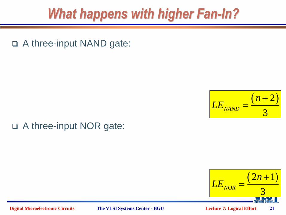
What happens with higher Fan-In?
A three-input NAND gate:
A three-input NOR gate:
21
2
3NAND
nLE
2 1
3NOR
nLE
Digital Microelectronic Circuits The VLSI Systems Center - BGU Lecture 7: Logical Effort
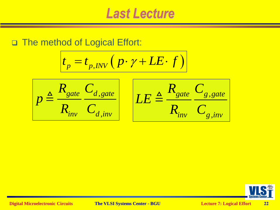
Last Lecture
The method of Logical Effort:
22
,p p INVt t p LE f
,
,
gate d gate
inv d inv
R Cp
R C
,
,
gate g gate
inv g inv
R CLE
R C
Digital Microelectronic Circuits The VLSI Systems Center - BGU Lecture 7: Logical Effort
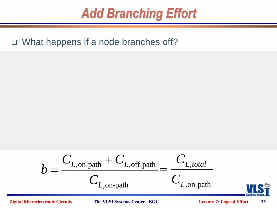
Add Branching Effort
What happens if a node branches off?
23
,on-path ,off-path
,on-path
L L
L
C Cb
C
,
,on-path
L total
L
C
C
Digital Microelectronic Circuits The VLSI Systems Center - BGU Lecture 7: Logical Effort
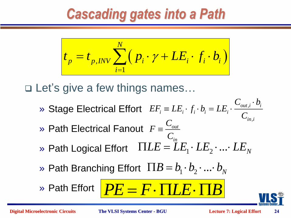
Cascading gates into a Path
Let’s give a few things names…
» Stage Electrical Effort
» Path Electrical Fanout
» Path Logical Effort
» Path Branching Effort
» Path Effort
24
,
1
N
p p INV i i i i
i
t t p LE f b
out
in
CF
C
1 2 ... NLE LE LE LE
1 2 ... NB b b b
PE F LE B
,
,
out i i
i i i i i
in i
C bEF LE f b LE
C
Digital Microelectronic Circuits The VLSI Systems Center - BGU Lecture 7: Logical Effort
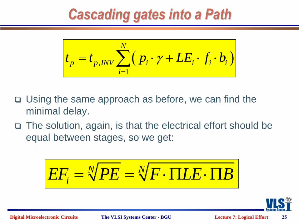
Cascading gates into a Path
Using the same approach as before, we can find the
minimal delay.
The solution, again, is that the electrical effort should be
equal between stages, so we get:
25
N N
iEF PE F LE B
,
1
N
p p INV i i i i
i
t t p LE f b
Digital Microelectronic Circuits The VLSI Systems Center - BGU Lecture 7: Logical Effort
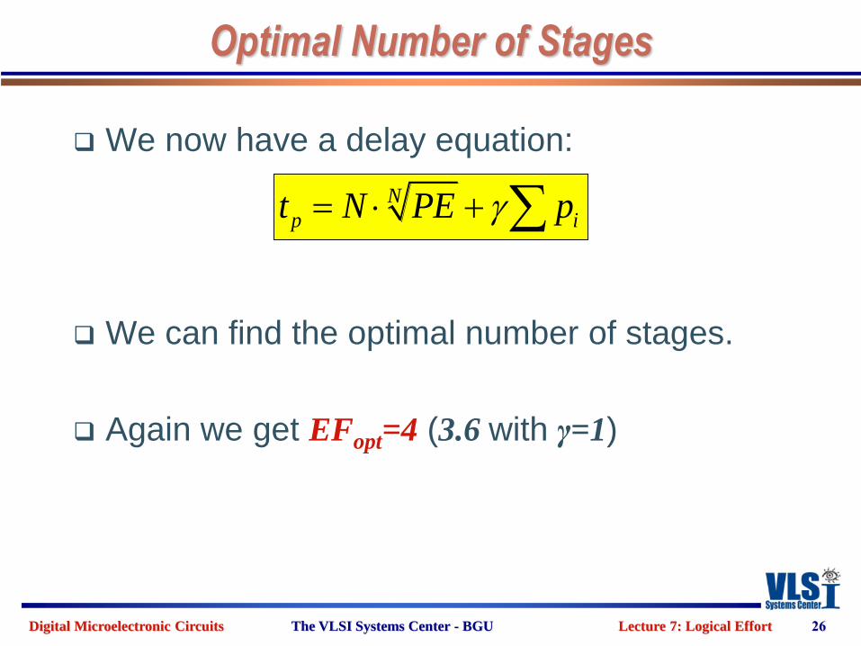
Optimal Number of Stages
We now have a delay equation:
We can find the optimal number of stages.
Again we get EFopt=4 (3.6 with γ=1)
26
N
p it N PE p
Digital Microelectronic Circuits The VLSI Systems Center - BGU Lecture 7: Logical Effort
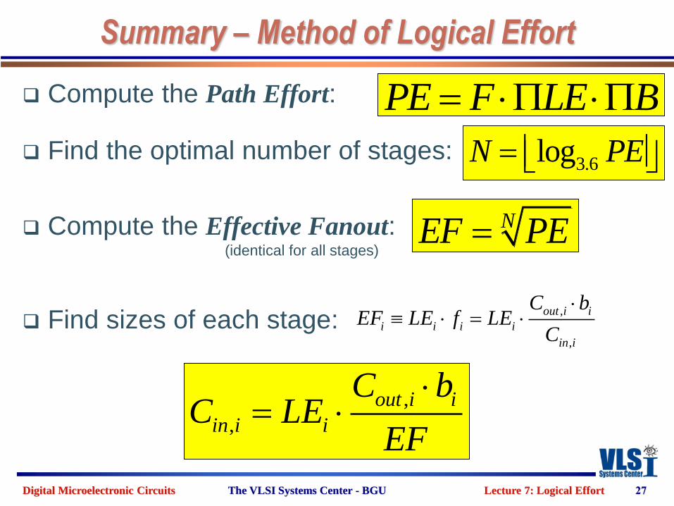
Summary – Method of Logical Effort
Compute the Path Effort:
Find the optimal number of stages:
Compute the Effective Fanout: (identical for all stages)
Find sizes of each stage:
27
PE F LE B
NEF PE
3.6logN PE
,
,
out i i
i i i i
in i
C bEF LE f LE
C
,
,
out i i
in i i
C bC LE
EF
Digital Microelectronic Circuits The VLSI Systems Center - BGU Lecture 7: Logical Effort
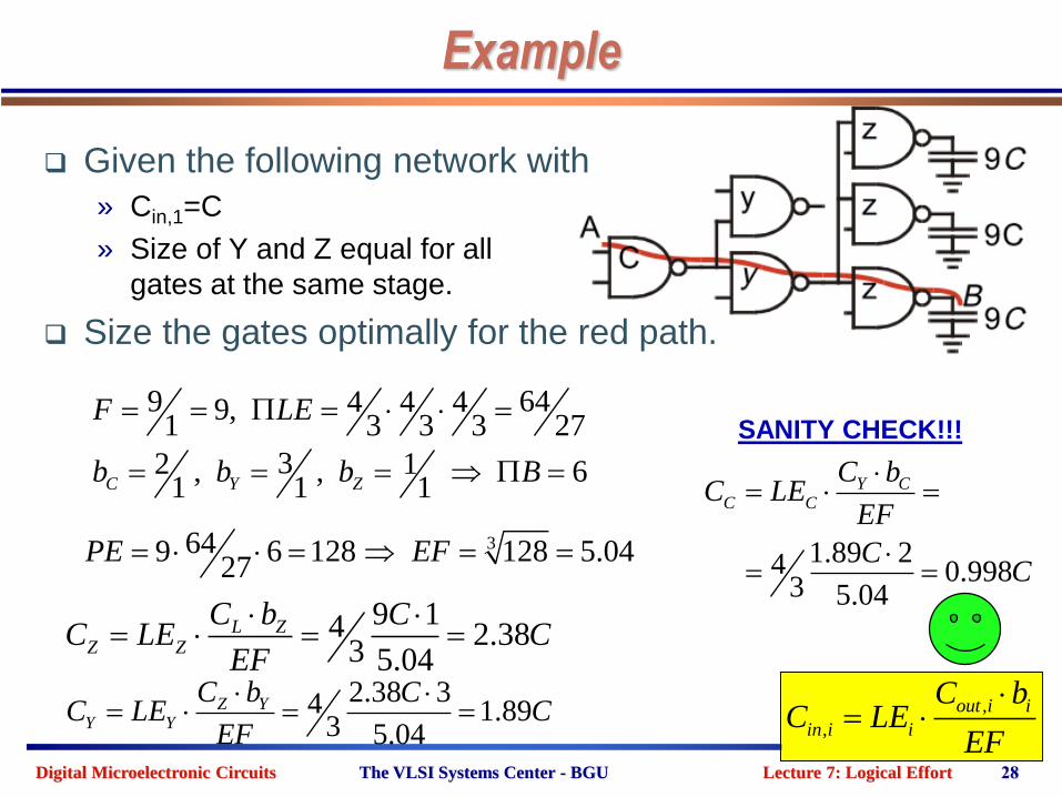
Example
Given the following network with
» Cin,1=C
» Size of Y and Z equal for all
gates at the same stage.
Size the gates optimally for the red path.
28
9 644 4 49,1 3 3 3 27
F LE
3649 6 128 128 5.0427
PE EF
32 1, , 61 1 1C Y Zb b b B
,
,
out i i
in i i
C bC LE
EF
9 14 2.383 5.04
L ZZ Z
C b CC LE C
EF
2.38 34 1.893 5.04
Z YY Y
C b CC LE C
EF
1.89 24 0.9983 5.04
Y CC C
C bC LE
EF
CC
SANITY CHECK!!!