Embed Size (px)
Citation preview

저 시-비 리- 경 지 2.0 한민
는 아래 조건 르는 경 에 한하여 게
l 저 물 복제, 포, 전송, 전시, 공연 송할 수 습니다.
다 과 같 조건 라야 합니다:
l 하는, 저 물 나 포 경 , 저 물에 적 된 허락조건 명확하게 나타내어야 합니다.
l 저 터 허가를 면 러한 조건들 적 되지 않습니다.
저 에 른 리는 내 에 하여 향 지 않습니다.
것 허락규약(Legal Code) 해하 쉽게 약한 것 니다.
Disclaimer
저 시. 하는 원저 를 시하여야 합니다.
비 리. 하는 저 물 리 목적 할 수 없습니다.
경 지. 하는 저 물 개 , 형 또는 가공할 수 없습니다.

1
Doctoral Thesis
Fabrication of Wet-Responsive Bioinspired
Adhesives and Their Applications
Hoon Yi
Department of Mechanical Engineering
Graduate School of UNIST
2020

2
Fabrication of Wet-Responsive Bioinspired
Adhesives and Their Applications
Hoon Yi
Department of Mechanical Engineering
Graduate School of UNIST

3
Fabrication of Wet-Responsive Bioinspired
Adhesives and Their Applications
A thesis
submitted to the Graduate School of UNIST
in partial fulfillment of the
requirements for the degree of
Doctor of Philosophy
Hoon Yi
Month/Day/Year of submission
Approved by
_________________________
Advisor
Hoon Eui Jeong

4
Fabrication of Wet-Responsive Bioinspired
Adhesives and Their Applications
Hoon Yi
This certifies that the thesis of Hoon Yi is approved.
December 10. 2019
signature
___________________________
Advisor: Hoon Eui Jeong
signature
___________________________
Heungjoo Shin
signature
___________________________
Young bin Park
signature
___________________________
Hyung wook Park
signature
___________________________
Moon kyu Kwak

i
ABSTRACT
Inspired by the fascinating adhesion properties of various creatures in nature, various bioinspired
adhesives have been developed. Since the bioinspired adhesives exhibit excellent adhesion strength and
reversible adhesion, they have strong potential for a wide variety of applications including wearable
devices, nanoscale manufacturing techniques, and soft robotics. However, the bioinspired adhesives
made of conventional elastomeric materials have limited adhesion strengths to rough surfaces and
limited controllability on adhesion strengths, which limits their practical applications. As the challenges
mainly result from the fixed physical property (e.g. elastic modulus of material) of the elastomer-based
adhesives, utilization of stimuli-responsive materials that enable active modulation of their mechanical
properties on demand is expected to be an effective solution overcoming the limitations.
Wet-responsive hydrogels are tunable in their shape, volume, and mechanical properties based on
hydration/dehydration in an active and reversible manner. Therefore, it is expected that bioinspired
adhesives made of the wet-responsive hydrogels could overcome the aforementioned challenges. In this
dissertation, we propose wet-responsive bioinspired adhesives made of hydroxypropyl cellulose (HPC)
hydrogel and polyethylene dimethacrylate (PEGDMA) hydrogel that exhibit superior surface
adaptability and high adhesion-on/off switchability, respectively.
For superior adaptability, a bioinspired adhesive comprised of wet-responsive HPC is proposed as it
enables adaptation to a rough surface due to its controllable swelling behavior. By
hydration/dehydration, the elastic modulus of the HPC hydrogel can be modulated on demand. In the
presence of a small amount of water, the individual bioinspired HPC microstructures in the adhesive
can be easily deformed along the rough surface with the decreased elastic modulus of the HPC. As
dehydrated, the elastic modulus of HPC microstructures is recovered with maintaining the deformed
morphology. Through these processes, the surface roughness-adapted HPC adhesive exhibits strong
adhesion strength. Furthermore, the adaptable HPC adhesive is reusable as the deformed
microstructures can recover their original shapes based on a shape-memory capability of HPC.
In order to develop the bioinspired adhesive that exhibits actively controllable and switchable
adhesion on demand, PEGDMA hydrogel with swelling behavior is utilized as it has shape-
reconfigurable property. The prepared PEGDMA adhesive shows high adhesion strengths against
substrates with the aid of bioinspired nano‐ or microstructure array in the dry state (adhesion-on state).
When the adhesive is exposed to water, a hydration‐induced shape transformation of the array and
macroscopic film bending occur, switching the adhesion off with an extremely high adhesion switching
ratio. Also, the switchable adhesion behavior of the adhesive is maintained over repeating cycles of

ii
hydration and dehydration, indicating their ability to be used repetitively.
As the rough surface adaptation and adhesion on/off properties of the developed adhesives only
require water droplets, they have a wide range of applications in diverse fields. Specifically, the
adhesives have a strong potential for use in a biomedical field as the HPC and PEGDMA hydrogels are
biocompatible. Accordingly, we demonstrate several unique biomedical practical applications of the
developed adhesives. Firstly, with the adaptable HPC adhesive, an attachable photonic skin is developed
as a wearable skin-like sensor. The photonic skin consisting of an HPC mechanochromic sensor and the
adaptable adhesive can firmly laminate to diverse substrates including human skins, detecting
mechanical signals from various target objects. Secondly, the adhesion-switchable PEGDMA adhesive
is utilized for a nanotransfer printing (nTP). We demonstrate that diverse metallic and semiconducting
nanomembranes can be transferred from donor substrates to either rigid or flexible surfaces including
biological tissues with the PEGDMA adhesive in a reproducible and robust fashion.
In total, this dissertation presents the fabrication of wet-responsive bioinspired adhesives and their
applications. The overall contents consist of three main themes, that are as follow: (1) fabrication of
bioinspired adhesives with optimized geometries, (2) rough surface-adaptable adhesive made of wet-
responsive HPC hydrogel and (3) adhesion-switchable adhesive made of wet-responsive PEGDMA
hydrogel.
Keywords: Bioinspired adhesive, Adhesion, Adaptable adhesive, Switchable adhesive, Wet-
responsive adhesive, Stimuli-responsive material, Wearable device, Transfer printing

iii

iv
CONTENTS
ABSTRACT ∙∙∙∙∙∙∙∙∙∙∙∙∙∙∙∙∙∙∙∙∙∙∙∙∙∙∙∙∙∙∙∙∙∙∙∙∙∙∙∙∙∙∙∙∙∙∙∙∙∙∙∙∙∙∙∙∙∙∙∙∙∙∙∙∙∙∙∙∙∙∙∙∙∙∙∙∙∙∙∙∙∙∙∙∙∙∙∙∙∙∙∙∙∙∙∙∙∙∙∙∙∙∙∙∙∙∙∙∙∙∙∙∙∙ i
CONTENTS ∙∙∙∙∙∙∙∙∙∙∙∙∙∙∙∙∙∙∙∙∙∙∙∙∙∙∙∙∙∙∙∙∙∙∙∙∙∙∙∙∙∙∙∙∙∙∙∙∙∙∙∙∙∙∙∙∙∙∙∙∙∙∙∙∙∙∙∙∙∙∙∙∙∙∙∙∙∙∙∙∙∙∙∙∙∙∙∙∙∙∙∙∙∙∙∙∙∙∙∙∙∙∙∙∙∙∙∙∙∙∙∙∙∙∙∙∙∙ iv
LIST OF TABLES ∙∙∙∙∙∙∙∙∙∙∙∙∙∙∙∙∙∙∙∙∙∙∙∙∙∙∙∙∙∙∙∙∙∙∙∙∙∙∙∙∙∙∙∙∙∙∙∙∙∙∙∙∙∙∙∙∙∙∙∙∙∙∙∙∙∙∙∙∙∙∙∙∙∙∙∙∙∙∙∙∙∙∙∙∙∙∙∙∙∙∙∙∙∙∙∙∙∙∙∙∙∙∙∙∙∙∙∙∙ vi
LIST OF FIGURES ∙∙∙∙∙∙∙∙∙∙∙∙∙∙∙∙∙∙∙∙∙∙∙∙∙∙∙∙∙∙∙∙∙∙∙∙∙∙∙∙∙∙∙∙∙∙∙∙∙∙∙∙∙∙∙∙∙∙∙∙∙∙∙∙∙∙∙∙∙∙∙∙∙∙∙∙∙∙∙∙∙∙∙∙∙∙∙∙∙∙∙∙∙∙∙∙∙∙∙∙∙∙∙∙∙ vii
NOMENCLATURE ∙∙∙∙∙∙∙∙∙∙∙∙∙∙∙∙∙∙∙∙∙∙∙∙∙∙∙∙∙∙∙∙∙∙∙∙∙∙∙∙∙∙∙∙∙∙∙∙∙∙∙∙∙∙∙∙∙∙∙∙∙∙∙∙∙∙∙∙∙∙∙∙∙∙∙∙∙∙∙∙∙∙∙∙∙∙∙∙∙∙∙∙∙∙∙∙∙∙∙∙∙∙∙ xiv
Chapter 1. Introduction ∙∙∙∙∙∙∙∙∙∙∙∙∙∙∙∙∙∙∙∙∙∙∙∙∙∙∙∙∙∙∙∙∙∙∙∙∙∙∙∙∙∙∙∙∙∙∙∙∙∙∙∙∙∙∙∙∙∙∙∙∙∙∙∙∙∙∙∙∙∙∙∙∙∙∙∙∙∙∙∙∙∙∙∙∙∙∙∙∙∙∙∙∙∙∙∙∙∙∙∙ 1
1-1. Research Background ∙∙∙∙∙∙∙∙∙∙∙∙∙∙∙∙∙∙∙∙∙∙∙∙∙∙∙∙∙∙∙∙∙∙∙∙∙∙∙∙∙∙∙∙∙∙∙∙∙∙∙∙∙∙∙∙∙∙∙∙∙∙∙∙∙∙∙∙∙∙∙∙∙∙∙∙∙∙∙∙∙∙∙∙∙∙∙∙∙∙∙∙∙∙∙∙ 1
1-2. Outline of Dissertation ∙∙∙∙∙∙∙∙∙∙∙∙∙∙∙∙∙∙∙∙∙∙∙∙∙∙∙∙∙∙∙∙∙∙∙∙∙∙∙∙∙∙∙∙∙∙∙∙∙∙∙∙∙∙∙∙∙∙∙∙∙∙∙∙∙∙∙∙∙∙∙∙∙∙∙∙∙∙∙∙∙∙∙∙∙∙∙∙∙∙∙∙∙∙ 7
Chapter 2. Fabrication of Bioinspired Adhesives with Optimized Geometries ∙∙∙∙∙∙∙∙∙∙∙∙ 9
2-1. Introduction ∙∙∙∙∙∙∙∙∙∙∙∙∙∙∙∙∙∙∙∙∙∙∙∙∙∙∙∙∙∙∙∙∙∙∙∙∙∙∙∙∙∙∙∙∙∙∙∙∙∙∙∙∙∙∙∙∙∙∙∙∙∙∙∙∙∙∙∙∙∙∙∙∙∙∙∙∙∙∙∙∙∙∙∙∙∙∙∙∙∙∙∙∙∙∙∙∙∙∙∙∙∙∙∙∙∙∙∙ 9
2-2. Results and Discussion ∙∙∙∙∙∙∙∙∙∙∙∙∙∙∙∙∙∙∙∙∙∙∙∙∙∙∙∙∙∙∙∙∙∙∙∙∙∙∙∙∙∙∙∙∙∙∙∙∙∙∙∙∙∙∙∙∙∙∙∙∙∙∙∙∙∙∙∙∙∙∙∙∙∙∙∙∙∙∙∙∙∙∙∙∙∙∙∙∙∙∙ 10
2-2-1. Fabrication of bioinspired adhesives with mushroom-shaped micropillars ∙∙∙ 10
2-2-2 Measurement and analysis of adhesion strength ∙∙∙∙∙∙∙∙∙∙∙∙∙∙∙∙∙∙∙∙∙∙∙∙∙∙∙∙∙∙∙∙∙∙∙∙∙∙∙ 15
2-3. Conclusion ∙∙∙∙∙∙∙∙∙∙∙∙∙∙∙∙∙∙∙∙∙∙∙∙∙∙∙∙∙∙∙∙∙∙∙∙∙∙∙∙∙∙∙∙∙∙∙∙∙∙∙∙∙∙∙∙∙∙∙∙∙∙∙∙∙∙∙∙∙∙∙∙∙∙∙∙∙∙∙∙∙∙∙∙∙∙∙∙∙∙∙∙∙∙∙∙∙∙∙∙∙∙∙∙∙∙∙∙∙ 19
Chapter 3. Wet-responsive adaptable adhesive ∙∙∙∙∙∙∙∙∙∙∙∙∙∙∙∙∙∙∙∙∙∙∙∙∙∙∙∙∙∙∙∙∙∙∙∙∙∙∙∙∙∙∙∙∙∙∙∙∙∙∙ 21
3-1. Introduction ∙∙∙∙∙∙∙∙∙∙∙∙∙∙∙∙∙∙∙∙∙∙∙∙∙∙∙∙∙∙∙∙∙∙∙∙∙∙∙∙∙∙∙∙∙∙∙∙∙∙∙∙∙∙∙∙∙∙∙∙∙∙∙∙∙∙∙∙∙∙∙∙∙∙∙∙∙∙∙∙∙∙∙∙∙∙∙∙∙∙∙∙∙∙∙∙∙∙∙∙∙∙∙∙∙∙∙ 21
3-2. Results and Discussion ∙∙∙∙∙∙∙∙∙∙∙∙∙∙∙∙∙∙∙∙∙∙∙∙∙∙∙∙∙∙∙∙∙∙∙∙∙∙∙∙∙∙∙∙∙∙∙∙∙∙∙∙∙∙∙∙∙∙∙∙∙∙∙∙∙∙∙∙∙∙∙∙∙∙∙∙∙∙∙∙∙∙∙∙∙∙∙∙∙∙ 22
3-2-1. Principle of wet-responsive adaptable adhesion ∙∙∙∙∙∙∙∙∙∙∙∙∙∙∙∙∙∙∙∙∙∙∙∙∙∙∙∙∙∙∙∙∙∙∙ 22
3-2-2. Ultra-adaptability of the adhesive ∙∙∙∙∙∙∙∙∙∙∙∙∙∙∙∙∙∙∙∙∙∙∙∙∙∙∙∙∙∙∙∙∙∙∙∙∙∙∙∙∙∙∙∙∙∙∙∙∙∙∙∙∙∙∙∙∙∙∙∙∙∙∙ 23

v
3-2-3. Theoretical analysis of the adhesion behavior of the adhesive∙∙∙∙∙∙∙∙∙∙∙∙∙∙∙∙∙∙∙∙∙ 26
3-2-4. Shape-memory capability of the adhesive ∙∙∙∙∙∙∙∙∙∙∙∙∙∙∙∙∙∙∙∙∙∙∙∙∙∙∙∙∙∙∙∙∙∙∙∙∙∙∙∙∙∙∙∙∙∙∙∙∙∙∙ 28
3-2-5. Application of the adhesive: Wearable photonic skin ∙∙∙∙∙∙∙∙∙∙∙∙∙∙∙∙∙∙∙∙∙∙∙∙∙∙∙∙∙∙∙∙∙∙ 30
3-3. Conclusion ∙∙∙∙∙∙∙∙∙∙∙∙∙∙∙∙∙∙∙∙∙∙∙∙∙∙∙∙∙∙∙∙∙∙∙∙∙∙∙∙∙∙∙∙∙∙∙∙∙∙∙∙∙∙∙∙∙∙∙∙∙∙∙∙∙∙∙∙∙∙∙∙∙∙∙∙∙∙∙∙∙∙∙∙∙∙∙∙∙∙∙∙∙∙∙∙∙∙∙∙∙∙∙∙∙∙∙∙∙∙ 35
3-4. Experimental Section ∙∙∙∙∙∙∙∙∙∙∙∙∙∙∙∙∙∙∙∙∙∙∙∙∙∙∙∙∙∙∙∙∙∙∙∙∙∙∙∙∙∙∙∙∙∙∙∙∙∙∙∙∙∙∙∙∙∙∙∙∙∙∙∙∙∙∙∙∙∙∙∙∙∙∙∙∙∙∙∙∙∙∙∙∙∙∙∙∙∙∙∙∙∙ 36
Chapter 4. Wet-responsive switchable adhesive ∙∙∙∙∙∙∙∙∙∙∙∙∙∙∙∙∙∙∙∙∙∙∙∙∙∙∙∙∙∙∙∙∙∙∙∙∙∙∙∙∙∙∙∙∙∙∙∙∙∙∙∙ 38
4-1. Introduction ∙∙∙∙∙∙∙∙∙∙∙∙∙∙∙∙∙∙∙∙∙∙∙∙∙∙∙∙∙∙∙∙∙∙∙∙∙∙∙∙∙∙∙∙∙∙∙∙∙∙∙∙∙∙∙∙∙∙∙∙∙∙∙∙∙∙∙∙∙∙∙∙∙∙∙∙∙∙∙∙∙∙∙∙∙∙∙∙∙∙∙∙∙∙∙∙∙∙∙∙∙∙∙∙∙∙∙∙ 38
4-2. Results and Discussion ∙∙∙∙∙∙∙∙∙∙∙∙∙∙∙∙∙∙∙∙∙∙∙∙∙∙∙∙∙∙∙∙∙∙∙∙∙∙∙∙∙∙∙∙∙∙∙∙∙∙∙∙∙∙∙∙∙∙∙∙∙∙∙∙∙∙∙∙∙∙∙∙∙∙∙∙∙∙∙∙∙∙∙∙∙∙∙∙∙∙∙ 39
4-2-1. Swelling behaviors of wet-responsive PEDGMA adhesive ∙∙∙∙∙∙∙∙∙∙∙∙∙∙∙∙∙∙∙∙∙∙∙∙∙∙∙∙∙∙∙∙∙∙∙ 39
4-2-2. Wet-responsive switchable adhesion property of the adhesive ∙∙∙∙∙∙∙∙∙∙∙∙∙∙∙∙∙∙∙∙∙∙∙ 45
4-2-3. Adhesion measurements of the adhesive ∙∙∙∙∙∙∙∙∙∙∙∙∙∙∙∙∙∙∙∙∙∙∙∙∙∙∙∙∙∙∙∙∙∙∙∙∙∙∙∙∙∙∙∙∙∙∙∙∙∙∙∙∙ 47
4-2-4. Application of the adhesive 1: Nanotransfer printing ∙∙∙∙∙∙∙∙∙∙∙∙∙∙∙∙∙∙∙∙∙∙∙∙∙∙∙∙∙∙∙∙∙∙∙∙∙ 51
4-2-5. Application of the adhesive 2: Transfer printing of nanocrack sensor ∙∙∙∙∙∙∙∙∙∙∙∙ 59
4-3. Conclusion ∙∙∙∙∙∙∙∙∙∙∙∙∙∙∙∙∙∙∙∙∙∙∙∙∙∙∙∙∙∙∙∙∙∙∙∙∙∙∙∙∙∙∙∙∙∙∙∙∙∙∙∙∙∙∙∙∙∙∙∙∙∙∙∙∙∙∙∙∙∙∙∙∙∙∙∙∙∙∙∙∙∙∙∙∙∙∙∙∙∙∙∙∙∙∙∙∙∙∙∙∙∙∙∙∙∙∙∙∙∙ 62
4-4. Experimental Section ∙∙∙∙∙∙∙∙∙∙∙∙∙∙∙∙∙∙∙∙∙∙∙∙∙∙∙∙∙∙∙∙∙∙∙∙∙∙∙∙∙∙∙∙∙∙∙∙∙∙∙∙∙∙∙∙∙∙∙∙∙∙∙∙∙∙∙∙∙∙∙∙∙∙∙∙∙∙∙∙∙∙∙∙∙∙∙∙∙∙∙∙∙∙ 62
Chapter 5. Conclusion ∙∙∙∙∙∙∙∙∙∙∙∙∙∙∙∙∙∙∙∙∙∙∙∙∙∙∙∙∙∙∙∙∙∙∙∙∙∙∙∙∙∙∙∙∙∙∙∙∙∙∙∙∙∙∙∙∙∙∙∙∙∙∙∙∙∙∙∙∙∙∙∙∙∙∙∙∙∙∙∙∙∙∙∙∙∙∙∙∙∙∙∙ 65
REFERENCES ∙∙∙∙∙∙∙∙∙∙∙∙∙∙∙∙∙∙∙∙∙∙∙∙∙∙∙∙∙∙∙∙∙∙∙∙∙∙∙∙∙∙∙∙∙∙∙∙∙∙∙∙∙∙∙∙∙∙∙∙∙∙∙∙∙∙∙∙∙∙∙∙∙∙∙∙∙∙∙∙∙∙∙∙∙∙∙∙∙∙∙∙∙∙∙∙∙∙∙∙∙∙∙∙∙∙∙∙∙ 66
ACKNOWLEDGMENTS ∙∙∙∙∙∙∙∙∙∙∙∙∙∙∙∙∙∙∙∙∙∙∙∙∙∙∙∙∙∙∙∙∙∙∙∙∙∙∙∙∙∙∙∙∙∙∙∙∙∙∙∙∙∙∙∙∙∙∙∙∙∙∙∙∙∙∙∙∙∙∙∙∙∙∙∙∙∙∙∙∙∙∙∙∙∙∙∙∙∙∙∙ 71

vi
List of Tables
Table 1-1. Various skin-attachable bioinspired adhesives
Table 1-2. Various switchable bioinspired adhesives
Table 4-1. Formulations of various PEGDMA solutions.
Table 4-2. Mechanical properties of PEGDMA having different molecular weights and
concentrations.
Table 4-3. Stability of the membranes with different thicknesses transferred onto the PEGDMA
adhesives with different stem diameters (Ds) of 400 nm, 5 µm, and 20 µm.
Table 4-4. Stability of the ribbon-type membranes with different thicknesses transferred onto
the PEGDMA adhesives with different stem diameters (Ds) of 400 nm, 5 µm, and 20 µm.

vii
List of Figures
Figure 1-1. Images of adhesive structures in various creatures and bioinspired adhesives and a
scheme showing advantages of the bioinspired adhesives.
Figure 1-2. Adaptable bioinspired adhesives based on (a) soft polyurethane, (b) low modulus
PDMS and (c) irreversibly cured polymer.
Figure 1-3. Figure 1-3. (a) Directionally controllable adhesion mechanism with slanted
nanohairs. (b) Switchable adhesion mechanism based on multi-step preload. (c) Controllable
detachment mechanism using an air pressure-based device.
Figure 2-1. (a) SEM images of bioinspired adhesives patterned with various shapes of
micropillars and (b) the adhesion strength measurement of the adhesives.
Figure 2-2. Schematic illustration for the fabrication of mushroom-shaped micropillars
through photolithography with a bilayer of SU-8 and LOR and a subsequent replica molding
with PDMS.
Figure 2-3. Photographs showing (a) the fabricated Si master and (b) bioinspired adhesive with
mushroom-shaped micropillar arrays. (c) Optical microscopy images of the fabricated
mushroom-shaped micropillars at five different regions, which correspond to locations i–iv
shown in (b). Each diameter depicted in the enlarged optical microscopy images is an averaged
value of ten micropillars in the location i–iv.
Figure 2-4. (a-d) Optical microscopy images of the Si masters with negative mushroom-shaped
micropillars fabricated through different LOR development times (a: no development, b: 60 s,
c: 180 s, d: 300 s). The tip diameter increased monotonically with the increase of development
time. (e-h) Cross-sectional scanning electron microscopy images of the fabricated Si masters,
which correspond to each array shown in a-d.
Figure 2-5. (a-d) Optical microscopy images of the mushroom-shaped micropillars with
different tip diameters replicated from the Si masters shown in Figure 2-4a-d. (e-h) Tilted
scanning electron microscopy images of the fabricated micropillars, which correspond to each
array shown in a-d. Insets in each image are magnified views of each image.

viii
Figure 2-6. Tip diameters of fabricated negative mushroom-shaped micropillars depending on
LOR development time for 4 different thick LOR layers.
Figure 2-7. Schematic and photograph of adhesion measurement system.
Figure 2-8. Measurement of the pull-off strength of mushroom-shaped micropillars with
different tip diameters for four different tip thicknesses of (a) ~1.15 μm, (b) ~2.10 μm, (c) ~2.75
μm and (d) ~4.05 μm. The tip diameters of the micropillars were controlled by modulating the
LOR development time during the Si master fabrication process.
Figure 2-9. Measurements of the pull-off strength of mushroom-shaped micropillars having
different tip diameters for four different tip thicknesses together with the theoretical predictions.
Figure 2-10. (a-d) Durability test of the fabricated mushroom-shaped micropillars with
different tip geometries of (a) ~1.15 μm tip thickness and ~22.7 μm tip diameter, (b) ~2.75 μm
thickness and ~22.5 μm diameter, (c) ~1.15 μm thickness and ~28.0 μm diameter and (d) ~2.75
μm thickness and ~29.5 μm diameter. Insets in figures (a-d) are detailed geometries of each
micropillar used for the corresponding durability tests. Inset in figure (c) is a magnified view
of the pull-off strength at 1–10 test cycles. (c-d) SEM and optical microscopy images of (e)
micropillars with ~1.15 μm tip thickness and ~28.0 μm tip diameter and (f) micropillars with
~2.75 μm thickness and ~29.5 μm diameter before (left image) and after (right image) the
measurement tests.
Figure 3-1. (a) photograph and SEM image of the fabricated HPC adhesive, (b) schematics
showing adaptable adhesion of the adhesive, (c) Swelling ratio (w/wi) of the crosslinked HPC
as a function of time and (d) stress-strain curves of the crosslinked HPC with different degrees
of swelling.
Figure 3-2. (a) Photographs showing PDMS adhesive and adapted HPC adhesive adhering
onto a paper, (b) measurement of normal adhesion strength of the PDMS, non-adapted HPC
and adapted HPC adhesive onto glass and paper surfaces under a preload of 50 kPa. (c)
Measurement of normal adhesion strengths of the PDMS, non-adapted HPC and adapted HPC
adhesives onto various substrates with different RMS values. (d) averages of normal adhesion
strengths of the adhesives. (e) measurement of peeling strength of the adapted HPC adhesives
onto various substrates. (f) averages of peeling energies of the adhesives.

ix
Figure 3-3. SEM image of the fabricated HPC adhesive attached to a paper.
Figure 3-4. (a) Repeatability test results showing the normal adhesion strength of the adapted
HPC adhesive against a paper substrate (20 cycles). For the single cycle measurement, the
hydrated HPC adhesive was applied to the substrate, followed by the adhesion measurement.
Subsequently, the HPC adhesive was removed from the substrate and then rehydrated with
water vapor. The rehydrated HPC adhesive was applied to the substrate again for the next
adhesion measurement. (b) a cycle of measurement of the normal adhesion strength of the
adapted HPC adhesive.
Figure 3-5. Normalized normal adhesion strengths that represent the relative adhesions of the
PDMS adhesives compared to those of the adapted HPC adhesives for diverse rough substrates
with gradually increasing RMS values.
Figure 3-6. Schematics of the series of swelling, adaptation, fixation and restoration of the
HPC adhesives.
Figure 3-7. (a) SEM and (b) optical microscope images showing the adaptation and restoration
performance of the HPC microstructures for a paper substrate with microscale surface
roughness. (c) SEM and (d) optical microscope images showing the adaptation and restoration
performance of the HPC microstructures for nanopatterned substrate with a regular nanopillar
array (pillar diameter: 500 nm, pitch 5 μm)
Figure 3-8. Optical microscope images (side view) showing the adaptation and shape recovery
performance of the HPC microstructures by applied
Figure 3-9. (a) Materials and principle of the photonic sensor layer based on chiral nematic
liquid crystal HPC. (b) Photograph of the stretched, large-area photonic skin. Inset shows the
unstretched photonic skin. (c) Photograph showing the HPC adhesive layer of the photonic
skin. Inset shows the SEM image of the microstructures of the adhesive layer; inset scale bar:
10 μm. (d) Schematic showing the multiple structural layers comprising of the photonic skin.
Figure 3-10. Detection of human motions and postures with the large-area (10 × 10 cm2)
multipixel (14 × 14) HPC photonic skin attached to a volunteer’s arm. Depending on the
motions and postures of the arm, the photonic skin exhibits distinct spatial color responses

x
(upper images). 3D stimuli-mapping data could be obtained from the color distributions in the
photonic skin via digital camera imaging and subsequent image processing (lower images).
Figure 3-11. (a) Color responses of the photonic skin attached to a model plate under different
bending strains. (b) Color responses of the photonic skin attached to a model cable under
different tensile strains.
Figure 3-12. Color responses of the photonic skin attached to gas pipes. The photonic skin can
immediately detect any leakage along the pipe via the intuitive color changes. (a) schematic
illustration showing the measurement of the pressure. (b) photonic skins attached to gas pipes.
(c) color responses of the photonics skin measuring the pressures.
Figure 4-1. (a) Schematic of the fabrication of the wet-responsive PEGDMA adhesives. Photo
and SEM images of the fabricated the adhesives: (b) Ds: 400 nm, (c) Ds: 5 μm and (d) Ds: 20
μm. (e) Conceptual illustration of the reversible hydration and dehydration process of the
PEGDMA bioinspired structure.
Figure 4-2. (a) Optical microscopy images showing the top views of the PEGDMA
microstructure (initial tip diameter: 24.3 μm, initial stem diameter: 20 μm, initial height: 20.4
μm) during the hydration and dehydration process. Dehydration was achieved by heating on a
hot plate (30 °C). (b) Optical microscopy images showing the side views of the PEGDMA
microstructure during the hydration and dehydration processes.
Figure 4-3. (a) Tip diameter and (b) height of the PEGDMA microstructures with 20 and 5 μm
stem diameters as a function of swelling time. Ratios of variations in the (c) tip diameter and
(d) height of the microstructures as a function of swelling time.
Figure 4-4. (a) Time-lapse photography showing the hydration-induced spontaneous bending
of the PEGDMA adhesive film and reflattening of the adhesive during dehydration at 30 °C.
Hydration-induced bending of the PEGDMA adhesives with different PET thicknesses: (b) 125
μm PET, (c) 50 μm PET and (d) 2 μm PET. (e) Radius of curvature of the adhesive film as a
function of PET film thickness. (f) Radius of curvature of the adhesives made from different
concentrations of PEGDMA on 50-μm-thick PET films.
Figure 4-5. (a) Tip diameter and (b) height of the PEGDMA microstructures with 20 and 5 μm

xi
stem diameters as a function of swelling time. Ratios of variations in the (c) tip diameter and
(d) height of the microstructures as a function of swelling time.
Figure 4-6. Optical microscope images showing the spontaneous detachment process of the
adhesive attached to a glass substrate by the reconfigurations of the adhesive film structure in
response to water penetration.
Figure 4-7. (a) Photographs of the PEGDMA adhesives bearing a significant weight of 6 kg
dumbbell for a long period of time in the dry state. (b) Conceptual illustration showing the
components for the hanging of loads to the PEGDMA adhesive. (c) Time-lapse photography
showing the detachment of the PEGDMA adhesive holding a weight of 100 g in response to
water penetration. In contact with water, the PEGDMA adhesive lost the adhesion within 30 s.
Figure 4-8. (a) Tip diameter and (b) height of the PEGDMA microstructures with 20 and 5 μm
stem diameters as a function of swelling time. Ratios of variations in the (c) tip diameter and
(d) height of the microstructures as a function of swelling time.
Figure 4-9. Tensile stress-strain curves of PEGDMA with MW of 750 and 550 of various
concentrations.
Figure 4-10. Adhesion strengths of the PEGDMA adhesives with different stem diameters
during repeated swelling and deswelling cycles. For the durability tests, PEGDMA adhesives
were swollen with water for 30 s followed by drying on a hot plate (30 °C).
Figure 4-11. (a) Conceptual illustration of the transfer printing of nanomembranes using the
wet-responsive PEGDMA adhesives. (b) Transfer printing of a patterned Au membrane
(thickness: 400 nm) from the donor substrate (Si wafer) to the receiver substrate (glass) using
the wet-responsive and reconfigurable PEGDMA adhesive. Upon contact with water, the
patterned Au membrane on the surface of the PEGDMA adhesive could be smoothly released
from the adhesive surface by the hydration-triggered spontaneous macroscopic film bending
and nano/microscopic shape transformations of the adhesive array. Inset in (viii) is a surface
profile image measured by AFM that shows the thickness of the Au membrane.
Figure 4-12. Optical microscopy and AFM images showing the transfer printing process of Au
nanoribbons (thickness: 200 nm, width: 28 µm, space: 12 µm) from an Si wafer to an SiO2

xii
wafer (1-µm-thick SiO2 layer on Si wafer) via the PEGDMA adhesive. AFM images show the
top- and cross-sectional views of the Au membrane before and after transfer printing. Before
transfer printing, the Au nanoribbons were formed on a patterned photoresist (thickness: 1.2
µm)
Figure 4-13. (a) Ag nanoribbons (thickness: 200 nm, line width: 20 µm, space: 20 µm)
transferred onto a PET film. (b) Cu nanoribbons (thickness: 200 nm, line width: 10 µm, space:
50 µm) transferred onto a polyimide film. (c) Si micromembranes (thickness: 2 µm) with
microhole arrays (diameter: 30 µm) formed on a PVC film. (d) Zig-zag shaped Au (thickness:
200 nm)-PUA (thickness: 5 µm) composite membranes transferred onto a curved glass cylinder.
Figure 4-14. SEM images of the double stacked Si line patterns formed by utilizing the
PEGDMA adhesives.
Figure 4-15. (a) Conceptual illustration of the Si nanoribbon transistor fabricated on a SiO2/Si
substrate based on nTP with the hydrogel adhesives. (b) SEM image, (c) VGS-IDS curve, and
(d) IDS-VDS curve of the Si nanomembrane FET transistor fabricated by the conventional
photolithographic process. (e) SEM image, (f) VGS-IDS curve, and (g) IDS-VDS curve of the
Si nanomembrane FET transistor fabricated by nTP with PEGDMA adhesives.
Figure 4-16. (a) Ag nanoribbons (thickness: 200 nm, line width: 25 µm, space: 120 µm)
transferred onto a plant leaf. (b) Pt (thickness: 50 nm)-SU-8 (thickness: 400 nm) composite
membranes transferred onto human skin. The transferred membrane was firmly attached to the
skin during both (i) tension and (ii) compression of the skin. (c) Au (thickness: 100 nm)-SU-8
(thickness: 400 nm) composite membranes transferred onto a porcine heart.
Figure 4-17. (a) Schematic illustration of the fabrication of the nanoscale crack sensor and its
subsequent transfer printing onto a bovine eye using the PEGDMA adhesive with saline
solution. (b) Conceptual illustration of the nanocrack sensor in which nanoscale cracks were
formed in the Pt layer (thickness: 20 nm) coated on the SU-8 layer (thickness: 2 µm). (c)
Conceptual illustration of the detection of the IOP using the sensor (d) Photograph of the
fabricated nanocrack sensor. AFM images on the right show the morphology of the nanocrack.
The nanocracks have an average width of ≈100 nm and depth of ≈35 nm. (e) Photograph of the
nanocrack sensor transferred onto a bovine eye.

xiii
Figure 4-18. (a) Normalized resistance variations measured with the transferred nanocrack
sensor during repetitive cycles of loading and unloading of pressure (40 mmHg). (b)
Normalized resistance variations showing the reversible loading–unloading behaviors at
different pressures (10, 20, 30, and 40 mmHg). (c) Normalized resistance variations during
loading and unloading as a function of the IOP.
xiv
Nomenclature
Abbreviations
RMS Root mean square
Si Silicon
DRIE Deep reactive ion etching
SEM Scanning electron microscope
SOI Silicon-on-insulator
LOR Lift-off resist
UV Ultraviolet
PDMS Polydimethylsiloxane
HPC Hydroxypropyl cellulose
Cu Copper
PE Polyethylene
Al Aluminum
PVC polyvinyl chloride
CNT Carbon nanotube
PEGDMA Polyethylene glycol dimethacrylate
MW Molecular weight
wt Weight
AFM Atomic force microscope
Pt Platinum
Au Gold
Ag Silver
SiO2 Silicon dioxide
nTP Nanotransfer printing

1
Chapter 1. Introduction
1-1. Research Background
Many living organisms such as gecko lizards, beetles, and cephalopods have versatile and effective
adhesive structures on their skin (Figure 1-1). 1-6 Gecko lizards can freely climb on various surfaces
with the aid of numerous micro/nanoscale hairs on their feet owing to the van der Waals force
mechanism. 6-8 Accordingly various bioinspired adhesives have been developed, which exhibit excellent
adhesion strength, repeatability and reversible adhesion without any surface contamination (Figure 1-
1). 1-6 In contrast to conventional chemical-based adhesives that are sticky and non-reusable, the
bioinspired adhesive systems with effective adhesion properties have significant potential various
applications including biomedical and precision manufacturing fields.
Figure 1-1. Images of adhesive structures in various creatures and bioinspired adhesives, and a scheme
showing advantages of bioinspired adhesives. 6-11
Firstly, for biomedical applications, bioinspired adhesives can be used as an adhesive layer of
wearable devices with biosensors and drug delivery systems. A number of studies have reported
adaptable bioinspired adhesives that are attachable to rough surfaces including human skin. As seen in
Figure 1-2a and b, an approach to develop adaptable bioinspired adhesives is utilization of highly soft
materials to fabricate the bioinspired adhesives. 12-13 Adhesives made of soft materials were conformally
attachable to rough surfaces, as the bioinspired microstructures could be deformed along the
morphology of the target surface. Nevertheless, these adhesives exhibited limited adhesion strength.
The adhesive in figure 1-3a showed an adhesion strength of ~60 kPa on a surface of root mean square
(RMS) height ~408 nm and the adhesive in figure 1-3b exhibited an adhesion strength of ~18 kPa on

2
skin. The limited adhesion strength is attributed to the low elastic moduli of the materials. The adhesion
strength of the bioinspired structure (mushroom-shaped micropillar) is given by 8
𝑃 = 𝑛(𝜋𝑤12𝐸∗/2𝑎)1
2𝑅2 (1-1)
where n is the density of the cylindrical microstructure, W12 is the work of adhesion, R is the radius of
the cylindrical flat punch, a is the defect radius, and A is the contact area. E* is the effective modulus,
expressed as E* = E/(1-ν2) where E is the elastic modulus and ν is Poisson’s ratio. As shown in the
equation, the low modulus of the soft material results in a limited adhesion strength of the adhesive.
Another research group proposed a different strategy to develop an adaptable bioinspired adhesive.
Firstly, at the ends of micropillars, a liquid prepolymer was coated by an inking technique. The coated
micropillars were sequentially attached onto a rough surface and cured to form mushroom-shaped
bioinspired micropillars (Figure 1-2c). 14 The bioinspired adhesive fabricated in this manner could be
conformally attached to the rough surface, resulting in reliable adhesion strength. However, the adhesive
could not be reused because the material was an irreversibly cured. Although skin-attachable bioinspired
adhesives have been extensively studied, they exhibit relatively low adhesion strength, as shown in
Table 1-1.

3
Figure 1-2. Adaptable bioinspired adhesives based on (a) soft polyurethane, (b) low elastic modulus
Polydimethylsiloxane (PDMS), and (c) irreversibly cured polymer. 12-14
Table 1-1. Various skin-attachable bioinspired adhesives
Shape Adhesion strength
(kPa)
Reference
Mushroom-shaped micropillars ~ 20 [12]
Mushroom-shaped micropillars ~ 15 [15]
Suction cup-like microstructure ~ 2 [16]
Suction cup-like microstructure ~ 22 [17]
Flat punch micropillars ~ 5 [18]

4
Secondly, in the case of precision manufacturing, bioinspired adhesives have been reported as smart
transport/holding systems that can precisely transfer diverse materials without chemicals. 19 For this
application, switchable bioinspired adhesive systems showing adhesion-on/off switchability have been
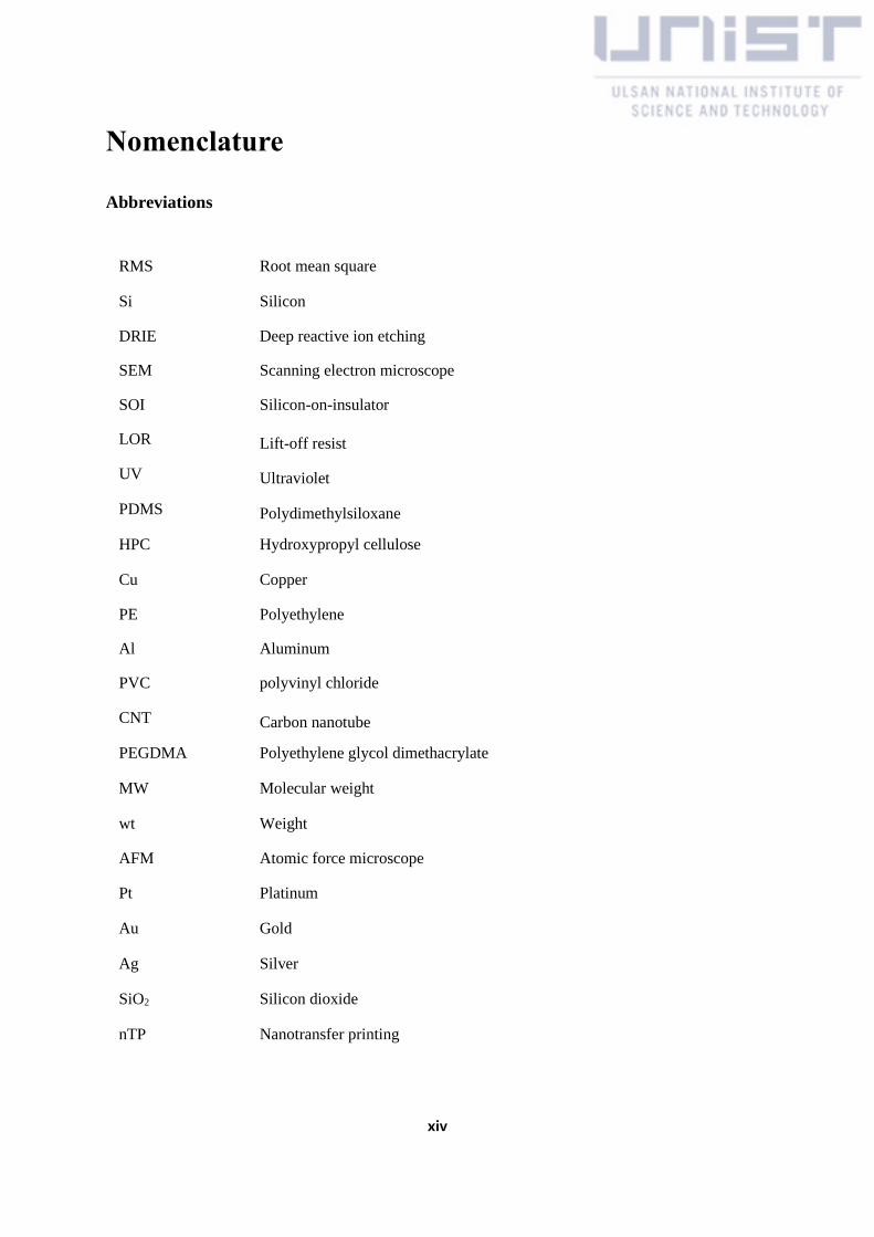
proposed. 20 Figure 1-3a shows a switchable bioinspired adhesive system utilizing gecko-inspired
slanted nanohairs. 7 This adhesive showed high adhesion strength when pulled against the direction of
the inclined angle (forward direction); however, it could be easily detached in the reverse direction. The
developed switchable adhesives showed an adhesion switching ratio (𝐴𝑑ℎ𝑒𝑠𝑖𝑜𝑛 𝑠𝑡𝑟𝑒𝑛𝑔𝑡ℎ𝑜𝑛 𝐴𝑑ℎ𝑒𝑠𝑖𝑜𝑛 𝑠𝑡𝑟𝑒𝑛𝑔𝑡ℎ 𝑜𝑓𝑓⁄ )
of ~13 and demonstrated the transport of a glass panel. As seen in figure 1-3b, a switchable bioinspired
adhesive system based on the buckling of adhesive micropillars was also proposed. 21-22 In this system,
the mechanical buckling of the micropillar occurs under a high compressive load, showing an adhesion
switching ratio of ~3. Another research group proposed a membrane patterned with adhesive
micropillars for the switchable bioinspired adhesion system (Figure 1-3c). The switchable adhesion
capability of this research was based on a macroscopic deformation of the membrane induced by an air
pump device. When the adhesive membrane was released without air pressure, it could adhere to and
pick up a target substrate with high adhesion strength. As the positive air pressure was applied, the
membrane was stretched and expanded. This expansion allowed the adhesive micropillars connected to
the substrate to be sequentially detached. This switchable adhesive device demonstrated the transport
of various substrates. 23
Meanwhile, with advances in electronic, semiconductor and biomedical devices, functional micro-or
nanomembranes must be transferred onto unconventional substrates such as flexible polymer, nonplanar
surfaces, and even biological tissues. Although novel switchable bioinspired adhesion systems based
on unique mechanical behaviors of bioinspired adhesive structures demonstrate the applications in the
transportation of various substrates, limitations remain. However, the previously developed adhesive
systems exhibited limited adhesion on/off switchability (low adhesion switching ratio) and required an
external mechanical load (table 1-2). Therefore, the existing systems have application difficulties for
the transfer of micro- or nanomaterials such as thinmembrane. Moreover, the external mechanical load
inducing the switchable adhesion could damage the materials and substrates. 24-33
5
Figure 1-3. (a) Directional adhesion mechanism with slanted nanohairs. (b) Switchable adhesion
mechanism based on multi-step preload. (c) Controllable detachment mechanism using an air pressure-
based device. 7, 21-23
Table 1-2. Various switchable bioinspired adhesives
Mechanism Adhesion switching ratio
(𝐴𝑑ℎ𝑒𝑠𝑖𝑜𝑛 𝑠𝑡𝑟𝑒𝑛𝑔𝑡ℎ𝑜𝑛
𝐴𝑑ℎ𝑒𝑠𝑖𝑜𝑛 𝑠𝑡𝑟𝑒𝑛𝑔𝑡ℎ 𝑜𝑓𝑓)
Reference
Directional adhesion ~13 [7]
Mechanical buckling ~3 [21]
Mechanical buckling ~4 [22]
Mechanical bending ~204 [23]
Directional adhesion ~2 [34]
Directional adhesion ~4 [35]

6
To overcome these limitations, we propose the following bioinspired adhesives utilizing wet-
responsive hydrogels that have tunable shape, volume, and mechanical properties based on
hydration/dehydration in an active and reversible manner:
(1) A bioinspired adhesive that exhibits superior adaptability, high adhesion strength, and reversible
adhesion property against various rough surfaces.
(2) A bioinspired adhesive that exhibits actively controllable, switchable, and reversible adhesion
capabilities with a high adhesion switching ratio.
In this dissertation, we present the fabrication of wet-responsive bioinspired adhesives and their
applications. Firstly, we develop a simple and reliable fabrication method for optimized bioinspired
adhesives. Next, we develop an ultra-adaptable bioinspired adhesive based on wet-responsive
hydroxypropyl cellulose (HPC) hydrogels and novel wearable photonic skin. Finally, we develop
actively controllable and switchable bioinspired adhesives based on wet-responsive polyethyleneglycol
dimethacrylate (PEGDMA) hydrogels and an efficient nanotransfer printing technique.
7
1-2. Outline of Dissertation
In chapter 2, we present a simple yet scalable fabrication technique with detailed protocols for
fabricating bioinspired adhesives with optimized mushroom-shaped micropillars. The fabricated
adhesives with a geometrically well-defined mushroom-shaped micropillar array were applied to wet-
responsive adhesives in chapter 3 and 4. A master with negative mushroom-shaped micropillars can be
generated through conventional photo-lithography by using commercially available photoresists. This
method enables simple and reliable fabrication of mushroom-shaped micropillars with precisely
controlled geometry of the micropillars. The fabricated bioinspired adhesives exhibited different
tendencies in adhesion strength and durability depending on the geometries. Adhesion measurements
of the fabricated bioinspired adhesives demonstrated that the geometry of the micropillars is critical to
obtain adhesion strength with superior and stable adhesion performance. With the results, we could
fabricate the bioinspired adhesive with optimized mushroom-shaped micropillars which not only
exhibit high durability but also show high adhesion strength.
In chapter 3, we present an ultra-adaptable bioinspired adhesive by employing a wet-responsive and
shape-memory HPC. Since they were reliably attachable onto highly rough substrates with only a small
amount of water, the adhesive is highly applicable to a variety of devices. Specifically, the developed
adaptable bioinspired adhesives show strong potential for wearable devices, because they were not only
highly attachable onto human skin but also reusable with the shape-memory capability. To demonstrate
the potential, a novel photonic skin where the bioinspired adhesives were integrated with HPC photonic
sensors was developed. The photonic skin could firmly adhere to diverse biological and non-biological
surfaces including human skin and directly visualize the mechanical strains of surfaces, showing the
strong potential of the adaptable bioinspired adhesive for wearable devices.
In chapter 4, we present an adhesion-switchable bioinspired adhesive that exhibits switchable and
controllable adhesions on demand, by employing a wet-responsive and shape-reconfigurable PEGDMA.
The fabricated switchable adhesives showed high adhesion strength in the adhesion-on state (dry state).
When in contact with water, the nano/microscopic and macroscopic shape reconfigurations of the
adhesive occurred, which turned off the adhesion (~ 0.3 kPa) with a high adhesion switching ratio (>
640). The superior adhesion behaviors of the adhesive were maintained over repeating cycles of
hydration and dehydration, indicating their ability to be used repeatedly. The adhesives are made of a
biocompatible hydrogel and their extremely high adhesion-on/off can be controlled with water, enabling
the adhesives to be applicable to various materials and surfaces, including biological substrates. Based
on these smart adhesion capabilities, diverse metallic and semiconducting nanomembranes could be
transferred from donor substrates to either rigid or flexible surfaces including biological tissues in a

8
reproducible and robust fashion (nanotransfer printing technique). Transfer printing of a nanoscale-
crack sensor onto a bovine eye further demonstrates the potential of the switchable bioinspired adhesive
for use as a stimuli-responsive, smart, and versatile functional adhesive for nanotransfer printing.

9
Chapter 2. Fabrication of Bioinspired Adhesives with
Optimized Geometries
This chapter includes the published contents:
H. Yi, M. Kang, M. K. Kwak, and H. E. Jeong, ACS Appl. Mater. Interfaces. 2016, 8, 22671-22678.
Copyright © 2019 American Chemical Society.
2-1. Introduction
With advances in bioinspired adhesives, various bioinspired adhesive structures have been proposed
33, 36-41. As seen in figure 2-1, depending on the shapes of bioinspired adhesive structures, the bioinspired
adhesives exhibited significantly different adhesion performances. 42 The adhesion behavior of
micropillars of various shapes (e.g., micropillars with a flat tip, spherical tip, flat tip with rounded edges,
mushroom-shaped tip, spatula tip and concave tip) have been investigated (Figure 2-1). The research
results showed that the bioinspired adhesives with mushroom-shaped micropillars exhibit the highest
adhesion strength under all preload ranges. In particular, the micropillars with flat tips, spherical tips,
flat tips with rounded edges, and concave tips exhibited lower adhesion strength than flat surfaces
without any patterns, demonstrating that the optimization of the structures is important for superior
adhesion performance. With these results, mushroom-shaped microstructures have been proposed as an
efficient form for bioinspired adhesives. Furthermore, these structures have reportedly enhanced
stability compared to bioinspired nanopillars, enabling millions of cycles of repeatable attachments and
detachments while maintaining the adhesion strength. 19
Figure 2-1. (a) SEM images of bioinspired adhesives patterned with various shapes of micropillars and
(b) the adhesion strength measurement. 42

10
Therefore, to achieve superior adhesion performance and structural stability in wet-responsive
bioinspired adhesives, the adhesives must be fabricated with a mushroom-shaped micropillar array.
Also, because the adhesion strength of mushroom-shaped micropillars depends their geometry, 8 we
must define the optimized geometry of the mushroom-shaped micropillars for maximized adhesion
strength. To this end, a reliable and efficient fabrication method that can precisely control the geometries
of the structures is necessary.
A number of methods have been developed to obtain the mushroom-shaped micropillars. 19, 43-48 The
most widely used method is deep reactive-ion etching (DRIE) of silicon-on-insulator (SOI) wafer with
embedded SiO2 layer. 19, 45-46 In this method, negative patterns of mushroom-shaped micropillars are
generated on the SOI wafer by utilizing the notching effect of the embedded oxide layer between the
top and bottom Si substrates during DRIE process. However, although this method enables reliable and
reproducible fabrication of Si master with negative patterns of mushroom-shaped microstructures, the
high cost of the SOI wafer and the DRIE process serve as significant hindrances to the practical use. A
modified soft-lithographic technique has also been proposed to generate the mushroom-shaped
structures. In this method, micropillars with protruding tips are generated by inking technique with flat
or hemispherical tips. 43, 48 Although this approach is relatively simple and cost-effective, obtaining
uniform geometries of the mushroom-shaped micropillars over a large area is not easy, because of the
fluidic and viscous nature of uncured prepolymer.
To this end, in this chapter, we developed a simple and scalable fabrication process with detailed
protocols for generating bioinspired adhesives with mushroom-shaped micropillar arrays using widely
used photoresists and proposed the bioinspired adhesive with optimized shapes of micropillars by
analyzing the performances of the adhesives. In our approach, we utilized a bilayer stack of SU-8 and
LOR (lift-off resist supplied by Microchem Corp.) to fabricate a master with negative mushroom-
shaped micropillar arrays through conventional photolithography. And, replica molding process with
widely used polymers can be utilized to generate mushroom-shaped micropillars with precisely
controlled tip diameters and thickness. Adhesion performances of the fabricated mushroom-shaped
micropillars with different tip geometries were also investigated, to define the optimized bioinspired
adhesive with mushroom-shaped micropillars.
2-2. Results and Discussion
2-2-1. Fabrication of bioinspired adhesives with mushroom-shaped micropillars
Figure 2-2 shows a schematic for fabricating mushroom-shaped micropillar arrays. A LOR was spin-
coated on a Si wafer, which is used as a sacrificial layer to form an undercut for protruding tips of the
mushroom-shaped micropillars. The LOR is inert to most organic solvents and acids after baking at its
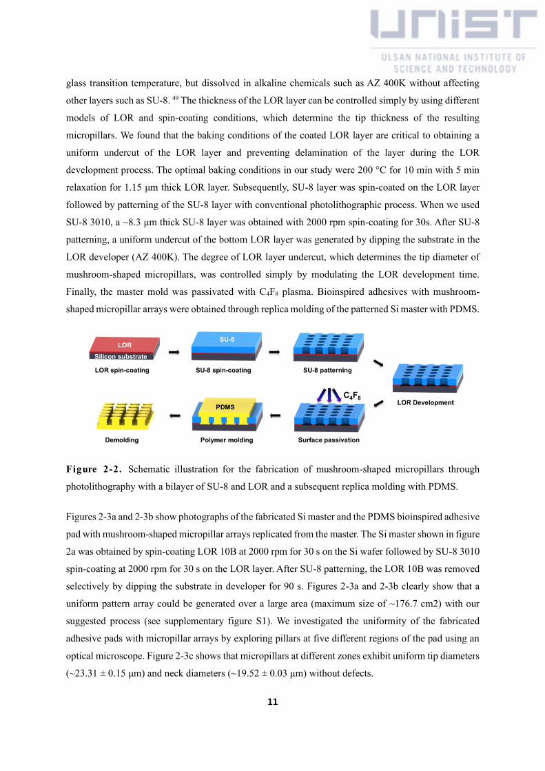
11
glass transition temperature, but dissolved in alkaline chemicals such as AZ 400K without affecting
other layers such as SU-8. 49 The thickness of the LOR layer can be controlled simply by using different
models of LOR and spin-coating conditions, which determine the tip thickness of the resulting
micropillars. We found that the baking conditions of the coated LOR layer are critical to obtaining a
uniform undercut of the LOR layer and preventing delamination of the layer during the LOR
development process. The optimal baking conditions in our study were 200 °C for 10 min with 5 min
relaxation for 1.15 μm thick LOR layer. Subsequently, SU-8 layer was spin-coated on the LOR layer
followed by patterning of the SU-8 layer with conventional photolithographic process. When we used
SU-8 3010, a ~8.3 μm thick SU-8 layer was obtained with 2000 rpm spin-coating for 30s. After SU-8
patterning, a uniform undercut of the bottom LOR layer was generated by dipping the substrate in the
LOR developer (AZ 400K). The degree of LOR layer undercut, which determines the tip diameter of
mushroom-shaped micropillars, was controlled simply by modulating the LOR development time.
Finally, the master mold was passivated with C4F8 plasma. Bioinspired adhesives with mushroom-
shaped micropillar arrays were obtained through replica molding of the patterned Si master with PDMS.
Figure 2-2. Schematic illustration for the fabrication of mushroom-shaped micropillars through
photolithography with a bilayer of SU-8 and LOR and a subsequent replica molding with PDMS.
Figures 2-3a and 2-3b show photographs of the fabricated Si master and the PDMS bioinspired adhesive
pad with mushroom-shaped micropillar arrays replicated from the master. The Si master shown in figure
2a was obtained by spin-coating LOR 10B at 2000 rpm for 30 s on the Si wafer followed by SU-8 3010
spin-coating at 2000 rpm for 30 s on the LOR layer. After SU-8 patterning, the LOR 10B was removed
selectively by dipping the substrate in developer for 90 s. Figures 2-3a and 2-3b clearly show that a
uniform pattern array could be generated over a large area (maximum size of ~176.7 cm2) with our
suggested process (see supplementary figure S1). We investigated the uniformity of the fabricated
adhesive pads with micropillar arrays by exploring pillars at five different regions of the pad using an
optical microscope. Figure 2-3c shows that micropillars at different zones exhibit uniform tip diameters
(~23.31 ± 0.15 μm) and neck diameters (~19.52 ± 0.03 μm) without defects.

12
Figure 2-3. Photographs showing (a) the fabricated Si master and (b) bioinspired adhesive with
mushroom-shaped micropillar arrays. (c) Optical microscopy images of the fabricated mushroom-
shaped micropillars at five different regions, which correspond to locations i–iv shown in (b). Each
diameter depicted in the enlarged optical microscopy images is an averaged value of ten micropillars in
the location i–iv.
The protruding tips of the mushroom-shaped micropillars are critical to obtaining high levels of pull-
off strength and durability of the pillar array. Therefore, precise tuning of the tip geometry of mushroom-
shaped micropillars is critical for the development of bioinspired adhesive with superior adhesion
performance. In our approach, the tip diameter can be modulated simply by controlling the development
time of the sacrificial LOR layer. Figures 2-4a-d show the optical microscope images of Si masters
fabricated with four different LOR development times (0s, 60s, 180 s, and 300 s). As shown in the
images, the outer diameter of the fabricated microholes was increased monotonically with the increase
of development time whereas the inner diameter of the holes remained almost the same, demonstrating
that the tip diameter of the array can be controlled precisely by modulating the development time of the

13
LOR layer. Figures 2-4e-h are the cross-sectional scanning electron microscope (SEM) images
corresponding to the optical microscopy images of figures 2-4a-d, which further confirm that
micropillars with varying tip diameters can be easily generated by controlling the degree of undercut of
the sacrificial LOR layer.
Figure 2-4. (a-d) Optical microscopy images of the Si masters with negative mushroom-shaped
micropillars fabricated through different LOR development times (a: no development, b: 60 s, c: 180 s,
d: 300 s). The tip diameter increased monotonically with the increase of development time. (e-h) Cross-
sectional scanning electron microscopy images of the fabricated Si masters, which correspond to each
array shown in a-d.
Figures 2-5a-d show optical microscope images of PDMS micropillar arrays replicated from the Si
master shown in figure 2-4. The tip diameter of micropillars replicated from a master without LOR
removal was ~19.4 μm. Tip diameters of the pillars were increased by using a master with longer LOR
development time of ~22.7 μm, ~25.5 μm, and ~28.0 μm for masters with 60 s, 180 s, 300 s development
times, respectively. Figures 2-5e-h show the tilted SEM images of the replicated mushroom-shaped
micropillars that correspond to optical microscopy images shown in figures 2-5a-d. The SEM images
also show that mushroom-shaped micropillars with controlled tip diameters can be generated by our
suggested process. The resulting pillar array has ~1.15 μm in tip thickness, ~9.4 μm total height and
~40 μm center-to-center pitch.

14
Figure 2-5. (a-d) Optical microscopy images of the mushroom-shaped micropillars with different tip
diameters replicated from the Si masters shown in Figure 2-4a-d. (e-h) Tilted scanning electron
microscopy images of the fabricated micropillars, which correspond to each array shown in a-d.
Insets in each image are magnified views of each image.
Figure 2-6 shows the tip diameters of the fabricated mushroom-shaped micropillars as a function of
LOR development time for samples with four different tip thicknesses ~1.15 μm, ~2.10 μm, ~2.75 μm
and ~4.05 μm). The maximum tip diameter that can be obtained from our master without damage was
about ~33.6 μm when the tip thickness was ~4.05 μm (length of the tip protruding out of the pillar post:
~7.67 μm). Tip thickness was modulated by controlling the speed of spin-coating using different kinds
of LOR. Although the undercut rate of the LOR layer was not perfectly linear, the tip diameters of the
resulting pillar arrays were increased monotonically for samples having four different tip thicknesses
with good reproducibility. Although samples with thicker tips required longer development time to
obtain the same tip diameters, mushroom-shaped micropillars with large variations in tip diameters of
up to ~ 12 μm could be simply generated with our approach. Controlling the tip diameter and tip
thickness of mushroom-shaped micropillars is not easily achievable with the aforementioned DRIE of
SOI wafer and the inking of micropillars with precured polymer. The difficulty arises from the notch
phenomenon being affected not only DRIE etching conditions but also by hole geometries, which in
turn, makes individually controlling the width and depth of the notch difficult. 45-46 Furthermore,
controlling the tip thickness requires the use of several SOI wafers with SiO2 layers of different
thicknesses, which will incur very high costs. In the case of the inking method, controlling the tip
diameter and thickness is also highly difficult because of the fluidic nature of the uncured polymer.
Although not demonstrated here, the height of the micropillars can also be controlled easily by changing
the spin-coated thickness of SU-8 layer.

15
Figure 2-6. Tip diameters of fabricated negative mushroom-shaped micropillars depending on LOR
development time for 4 different thick LOR layers.
2-2-2. Measurement and Analysis of adhesion strength
The adhesion strengths of the fabricated bioinspired micropillars were evaluated using custom-built
equipment. The bioinspired adhesive sample was attached to a flat substrate under controlled preload
(Figure 2-7). Figure 2-8 shows the pull-off strength of bioinspired adhesives with different tip diameters
and four different tip thicknesses (~1.15 μm, ~2.10 μm, ~2.75 μm and ~4.05 μm). For statistical
significance, adhesion measurement was carried out 20 times for each sample under identical conditions.
As shown in the figures, micropillars without tips exhibited very low adhesion strength (< ~1 N cm-2).
On the contrary, micropillars with protruding tips displayed drastically enhanced adhesion strength. For
example, bioinspired adhesive pads with a relatively thin tip (~1.15 μm thickness) and a tip diameter of
~20.2 μm (LOR development time: 30 s) had maximum pull-off strength of ~14 N cm-2 under a preload
of 20 N (figure 6a). The pull-off strength decreased after passing the maximum point due to the buckling
of the pillars or the later deformation of the back film under an excessive preload.17, 24, 33 The
maximum pull-off strength was increased further to ~21 N cm-2 and ~25 N cm-2 with the increase of tip
diameter to ~22.7 μm (LOR development time: 60 s) and ~25.5 μm (LOR development time: 180 s),
respectively (Figure 2-8a). These results indicate that the pull-off strength of bioinspired adhesives with
mushroom-shaped microstructures can be modulated by controlling the tip diameters of micropillars
without changing the pillar diameter and pitch. In theory, the pull-off force of for a micropillar with the
flat tip Pflat is given by 50
𝑃𝑝 = √8𝜋𝐸∗𝑟3𝑤12 (2-1)
where E* is the effective Elastic modulus of the system, and r is the radius of the flat tip. Here, w12 is
the work of adhesion of the interface. Although equation 2-1 is for the micropillar arrays with simple

16
flat tips, our experimental results are in a good agreement with the theoretical prediction (Figure 2-9).
Figure 2-7. Schematic and photograph of adhesion measurement system.
Figure 2-8. Measurement of the pull-off strength of mushroom-shaped micropillars with different
tip diameters for four different tip thicknesses of (a) ~1.15 μm, (b) ~2.10 μm, (c) ~2.75 μm and (d)
~4.05 μm. The tip diameters of the micropillars were controlled by modulating the LOR development
time during the Si master fabrication process.

17
Figure 2-9. Measurements of the pull-off strength of mushroom-shaped micropillars having different
tip diameters for four different tip thicknesses together with the theoretical predictions.
One notable feature of the results is that samples prepared with excessively long development time
(> 300 s) exhibited diminished pull-off strengths as compared with samples prepared with proper
development time (30–180 s). For example, samples prepared with 300 s LOR development time had
pull off strength of ~ 7 N cm-2 at best, which is merely ~25 % of the maximum strength, with fairly high
standard deviation ( ~2 - 8 N cm-2). This result is because although micropillars with thinner and larger
tips enable conformal and larger contact against a substrate, the mechanical stability and durability of
the pillars with thinner and larger tips decreased significantly. For example, mushroom-shaped
micropillars with ~1.15 μm tip thickness and ~28.0 μm tip diameter exhibited maximum adhesion
strength of ~30 N cm-2 during the first adhesion measurement test (Figure 2-8a). However, the averaged
pull-off values decreased to ~7 N cm-2 after 20 cycles of tests because of the low durability of the
excessive tip size. This averaged value is expected to decrease further with the increase in measurement
test cycles. In addition to the low averaged pull-off strength, these samples displayed high levels of
variations in pull-off strength even at the first adhesion test (Figure 2-8a). This is because the too thin
and large tips of the pillar arrays impeded conformal contact of the tips against a substrate because of
the wrinkling or folding of the tips during contact of the pad on a substrate.

18
Theoretical studies on the collapse of tips of mushroom-shaped micropillars has rarely been reported,
but some theoretical works on microfabricated structures have been presented. 51 On the basis of a
quantitative model of ground collapse of micropillars, the critical aspect ratio (AR), defined as the ratio
of the length of the tip (L) protruding out of the pillar post to tip thickness (t) for preventing the
wrinkling or folding of the tips, is given by
(𝐿
𝑡) = 18−1
2⁄ ∙ 𝜋 ∙ (𝐸
𝑤12)
12⁄ ∙ (𝑡)
12⁄ (2-2)
where E is the Elastic modulus of the material. According to equation 2-2, the critical AR (L/t) of the
protruding tips can be increased by increasing the tip thickness. Therefore, the problems associated with
the weak structural durability of the micropillars with large tips can be solved through a slight increase
in tip thickness. As shown in figure 6c, micropillars with ~2.75 μm tip thickness exhibited a high level
of averaged pull-off strength. For instance, the averaged pull-off strength of micropillars with ~22.4 μm
tip diameter (LOR-30B, development time: 300 s) reached ~17 N cm-2 and increased further to ~27 N
cm-2 with micropillars with ~29.5 μm tip diameter (LOR-30B, development time: 600 s) with small
standard deviations in the pull-off strength. The mushroom-shaped micropillars with thin and large tips
(~1.15 μm tip thickness and ~28 μm tip diameter) exhibited low averaged adhesion because of low
structural durability. However, increasing the tip thickness slightly to ~2.75 μm, micropillars with
similarly large tips (~29.5 μm tip diameter) had significant enhancements in structural durability and
more stable pull-off strength.
Repeatability of the mushroom-shaped micropillars with different tip geometries was further
investigated by carrying out durability tests, where the cycles of attachment and detachment were
repeated using bioinspired adhesives with different tip sizes (Figure 2-10). As shown in figure 2-10a
and b, when the tip diameter is relatively small (~22–23 μm), the micropillar arrays maintained their
pull-off strength even after 500 cycles of testing because the tip AR (L/t) is relatively small (0.64 –
1.38). However, when the tip diameter increased to ~28–30 μm, pull-off of micropillars with thinner
tips (AR: ~3.70) decreased immediately after the first adhesion measurement (figure 2-10c). In contrast,
micropillars with slightly thicker tips (AR: ~1.93) exhibited better durability as compared with
micropillars with thinner tips, although a slight decrease in pull-off was observed (Figure 2-10d). These
results can be easily understood because of the large and thinner tips of micropillars, which are
mechanically unstable and are therefore easily folded and collapsed upon the attachment and
detachment against a contact surface (Figure 2-10e). Micropillars with large but thicker tips maintain
their structural integrity and adhesion performance even after repeated cycles of attachment and
detachment (Figure 2-10f). Thus, fabrication of mushroom-shaped micropillars with optimized tip
geometry is critical to the development of bioinspired adhesives with superior and stable adhesion

19
performances.
Figure 2-10. (a-d) Durability test of the fabricated mushroom-shaped micropillars with different tip
geometries of (a) ~1.15 μm tip thickness and ~22.7 μm tip diameter, (b) ~2.75 μm thickness and
~22.5 μm diameter, (c) ~1.15 μm thickness and ~28.0 μm diameter and (d) ~2.75 μm thickness and
~29.5 μm diameter. Insets in figures (a-d) are detailed geometries of each micropillar used for the
corresponding durability tests. Inset in figure (c) is a magnified view of the pull-off strength at 1–10
test cycles. (c-d) SEM and optical microscopy images of (e) micropillars with ~1.15 μm tip thickness
and ~28.0 μm tip diameter and (f) micropillars with ~2.75 μm thickness and ~29.5 μm diameter
before (left image) and after (right image) the measurement tests.
2-3. Conclusion
In summary, we developed a simple yet scalable fabrication technique with detailed protocols for
fabricating bioinspired adhesives with mushroom-shaped micropillars with controlled tip diameter and
thickness. A master with negative mushroom-shaped micropillars can be generated through

20
conventional photolithography by utilizing a bilayer stack of top SU-8 layer and bottom sacrificial LOR
layer. The thickness and diameter of the mushroom-shaped tips can be controlled by modulating the
spin-coating thickness and development time of the LOR layer, which enables simple, reproducible,
and scalable fabrication of mushroom-shaped micropillars with precisely controlled tip geometry. The
fabricated mushroom-shaped micropillar arrays exhibit different tendencies in adhesion strength and
durability depending on the tip diameter and thickness of micropillars. Macroscopic adhesion
measurements of the fabricated bioinspired adhesives demonstrate that tip diameter and thickness of
the micropillars are critical to obtaining bioinspired adhesives with superior and stable adhesion
performances. Our bioinspired adhesives with optimized tip geometry exhibit high durability as well as
a high level of pull-off strength of up to ~34.8 N cm-2 on the Si surface. In chapter 3 and 4, we could
fabricate wet-responsive bioinspired adhesives showing excellent adhesion performances with this
optimized mushroom-shaped micropillars.
21
Chapter 3. Wet-responsive adaptable Adhesive
This chapter includes the published contents:
H. Yi†, S. -H. Lee†, H. Ko†, W. -G. Bae, T. -I. Kim, D. S. Hwang, and H. E. Jeong, Adv. Funct. Mat.
2019, 1902720. Copyright © 2019 Wiley.
3-1. Introduction
In wearable device with electronic sensor or photonic sensors, their intimate coupling to the skin is
of tremendous importance, as it determines the sensing quality, stability, and reliability while
minimizing the motion artifact. 52-56 However, a stable and robust adhesion to the skin is challenging,
as the skin not only is a dynamic surface with low surface energy (25-29 mJ m-2)57 but also possess
multiscale surface textures. To this end, soft sensors have been made with ultrathin film configuration,
with thickness less than 10 μm; as such thin-film devices can be firmly laminated to the skin by reducing
flexural rigidity based on van der Waals forces.56, 58 However, such thin-film devices are difficult to
handle and mechanically less durable. Further, they are difficult to reuse once they are applied onto the
skin.57 To this end, bioinspired adhesives that emulate the adhesion mechanisms of living organisms
have been suggested as effective adhesive components for skin-interfaced sensors.15, 52-53, 57 They have
demonstrated skin-friendly, biocompatible, and repeatable skin adhesion. However, they suffer from
relatively low adhesion strength (<15-20 kPa) compared to those of commercial skin adhesives (~30
kPa).52-53, 59 Furthermore, they have shown limited adaptability to surfaces with relatively high surface
roughness. For example, gecko- or beetle-inspired adhesives made of polydimethylsiloxane (PDMS),
which is one of the most widely used materials for prior bioinspired adhesives, cannot be firmly attached
to highly rough surfaces such as wrinkled skin, a painted wall, or paper. This is because the PDMS
microstructures have limited deformability and adaptability to highly rough surfaces.60-61 Wearable
sensors that are not only easy to handle but also can be intimately attached to virtually any surface of
biological and non-biological substrates with strong and reliable adhesion strength and without surface
damages and irritations still remain challenging.57, 62
Hydroxypropyl cellulose (HPC), one of the cellulose derivatives that are the most abundant
biopolymers on the earth, is a promising material having all desirable properties to address all
aforementioned issues. HPC is biodegradable, renewable, and biocompatible. 63-65 HPC can be
prepared in the form of amorphous-phase transparent hydrogel with controllable swelling behavior
and shape-memory capability,66 which can be utilized as an adaptable material for reversible
adhesives to diverse surfaces with varying roughness. All these features of HPC make it an ideal
candidate for developing biocompatible, flexible, reusable, and skin-mountable adhesive. Despite

22
such attractive advantages of HPC, few studies have addressed the development of cellulose-based
bioinspired adhesives.
In this chapter, we present an ultra-adaptable and wet-responsive adhesive that can reversibly adhere
to diverse substrates with crosslinked HPC. We demonstrated that this adaptable adhesive is reversibly
attachable to various rough surfaces, including skin, paper, plaster, copper (Cu), aluminum, polyvinyl
chloride (PVC), polyethylene (PE), and wood, with 5.4-183.7 times higher adhesion strengths compared
to those of the PDMS adhesive. With this adaptable adhesive, we develop an wearable photonic skin
that directly visualize the spatio-temporal distribution of external mechanical stimuli, 67-68 by
concurrently harnessing a photonic sensor made of liquid crystalline phase HPC and the ultra-adaptable
adhesive in a single device platform. Based on the high adaptability of the adhesive, this cellulose-based
photonic skin can display external stimuli with excellent sensing quality.
3-2. Results and Discussion
3-2-1. Principle of wet-responsive adaptable adhesion
To secure proper adhesion to rough surfaces, adhesive materials should have adequate viscoelastic
property. Pressure-sensitive adhesive (PSA) is a representative viscoelastic material that can make
adequate adhesions to diverse surfaces. 57 However, they are not optimal for prolonged, long-term
attachment to the skin due to PSA-induced skin damage and irritation. 57, 62 Although bioinspired
microstructures-based skin adhesives and skin-mountable sensors have been developed as alternatives,
they have limited adhesion strength and adaptability to rough surfaces. 52-53, 59 This is because many
previous bioinspired adhesives were made of elastomeric materials (e.g., PDMS and polyurethane
acrylate), which have relatively high elastic moduli (~1-20 MPa). 33, 36-41 Therefore, they cannot exhibit
proper liquid-like behavior for bonding formation to rough surfaces, which significantly limits their
adhesion performance to rough surfaces. Although elastomeric materials with relatively low elastic
modulus can be utilized for bioinspired adhesives, it can lead to structural instabilities and limit
mechanical durability. 57, 59
HPC hydrogel based-bioinspired microstructures can address this issue (Figure 3-1a and b). In a dried
state, the elastic modulus of the HPC hydrogel was 14.9 MPa (Figure 3-1c and d). Therefore, the
microstructure can exhibit a sufficient cohesive strength and maintain structural integrity. However,
when the HPC hydrogel was swollen with moisture for 180 s, its elastic modulus significantly decreased
to 0.21 MPa (Figure 3-1c and d). It is noted that this value is comparable to that of typical PSAs and
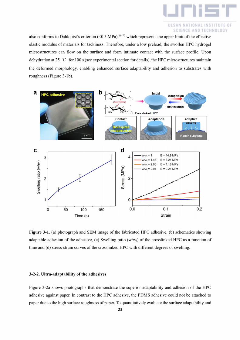
23
also conforms to Dahlquist’s criterion (<0.3 MPa),69-70 which represents the upper limit of the effective
elastic modulus of materials for tackiness. Therefore, under a low preload, the swollen HPC hydrogel
microstructures can flow on the surface and form intimate contact with the surface profile. Upon
dehydration at 25 ℃ for 100 s (see experimental section for details), the HPC microstructures maintain
the deformed morphology, enabling enhanced surface adaptability and adhesion to substrates with
roughness (Figure 3-1b).
Figure 3-1. (a) photograph and SEM image of the fabricated HPC adhesive, (b) schematics showing
adaptable adhesion of the adhesive, (c) Swelling ratio (w/wi) of the crosslinked HPC as a function of
time and (d) stress-strain curves of the crosslinked HPC with different degrees of swelling.
3-2-2. Ultra-adaptability of the adhesives
Figure 3-2a shows photographs that demonstrate the superior adaptability and adhesion of the HPC
adhesive against paper. In contrast to the HPC adhesive, the PDMS adhesive could not be attached to
paper due to the high surface roughness of paper. To quantitatively evaluate the surface adaptability and

24
adhesion performance of the integrated photonic skin, the adhesion strengths of the HPC adhesive were
measured against a variety of model substrates including glass, copper, PVC, plaster, paper, wood, and
skin (Figure 3-2b, c, d). The PDMS adhesive exhibited fairly high adhesion strength of 147.9 kPa
against a flat glass substrate, the surface roughness RMS of which was 52 nm (Figure 3-2b, c, d).
However, as the roughness of the substrates increased, the adhesion strength of the PDMS adhesive
notably decreased. For example, the adhesion strength of the PDMS adhesive on copper was
significantly reduced to 35.9 kPa, although the roughness of the copper was not significant (RMS: 0.54
μm). The PDMS adhesive exhibited negligible adhesion for other model substrates with higher surface
roughness (Figure 3-2c, d). Notably, the adhesion strengths of the adapted HPC adhesive were evaluated
after dehydrating the adhesive at 25 ℃ for 100 s. The adhesion strengths of the adapted HPC adhesive
for the copper, PVC, plaster, paper, wood, and porcine skin substrates were measured as 194.2 kPa,
212.2 kPa, 236.6 kPa, 252.4 kPa, 275.6 kPa, and 52.0 kPa, respectively, which are 5.4-183.7 times
higher values compared to those of the PDMS adhesive. For the glass substrate, the adhesion strength
of the adapted HPC adhesive was 184.1 kPa, which is just 1.24 times higher than that of the PDMS
adhesive (147.9 kPa). This is because the HPC and PDMS adhesives have similar contact areas for the
glass substrate, which has a nearly flat surface profile (RMS: 52 nm). To further evaluate the adhesion
performance of the HPC adhesive, we also investigated its peeling energy for the different substrates.
As shown in Figure 3-2e and f, the adapted HPC adhesive showed drastically enhanced peeling energy
for the wide range of rough surfaces compared with that of the non-adapted HPC adhesive. Figure 3-3
shows the SEM images of the non-adapted and adapted HPC microstructures against a paper surface.
As shown, due to the high surface roughness of paper, with RMS value of ~20 μm, the pristine HPC
adhesive could not form an intimate contact with the substrate (Figure 3-3a). In contrast, the swollen
HPC adhesive could conform to the irregular surface topography of the paper (Figure 3-3b). The strong
adhesion of the HPC adhesive was maintained over repetitive attachment and detachment cycles,
demonstrating reversible and repeatable adhesion properties of the adhesive (Figure 3-4).

25
Figure 3-2. (a) Photographs showing PDMS adhesive and adapted HPC adhesive adhering onto a paper,
(b) measurement of normal adhesion strength of the PDMS, non-adapted HPC and adapted HPC
adhesive onto glass and paper surfaces under a preload of 50kPa. (c) Measurement of normal adhesion
strengths of the PDMS, non-adapted HPC and adapted HPC adhesives onto various substrates with
different RMS values. (d) averages of normal adhesion strengths of the adhesives. (e) measurement of
peeling strength of the adapted HPC adhesives onto various substrates. (f) averages of peeling energies
of the adhesives.

26
Figure 3-3. SEM image of the fabricated HPC adhesive attached to a paper.
Figure 3-4. (a) Repeatability test results showing the normal adhesion strength of the adapted HPC
adhesive against a paper substrate (20 cycles). For the single cycle measurement, the hydrated HPC
adhesive was applied to the substrate, followed by the adhesion measurement. Subsequently, the HPC
adhesive was removed from the substrate and then rehydrated with water vapor. The rehydrated HPC
adhesive was applied to the substrate again for the next adhesion measurement. (b) a cycle of
measurement of the normal adhesion strength of the adapted HPC adhesive.
3-2-3. Theoretical analysis of the adhesion behavior of the adhesive
Figure 3-5 shows the comparison of the adhesions of the adapted HPC adhesive and PDMS
adhesive for diverse substrates with different RMS values. For the relative comparison, the
normalized adhesion strength (Pnorm) was defined as the measured adhesion strength of the adhesives
(P) divided by the adhesion strength of the adapted HPC adhesive (Pmax) for each type of rough
substrate (Pnorm = P/Pmax). Considering the surface roughness as close-packed hemispherical asperity
caps and troughs, 71-72 P for rough surfaces is given by

27
𝑃 =𝑛𝐴𝐻𝐴
6𝐻02 [𝜌𝑟 +
1
𝜋𝐻0(1+𝑦𝑚𝑎𝑥 𝐻0⁄ )3] (2-1)
where AH is the Hamaker constant, A is the area of the contact ends of the microstructure, H0 is the
equilibrium distance, ρ is the radius of the asperity of the substrate, r is the radius of the asperity, and
ymax is the height of the asperity. ρ and ymax can be expressed as 71-72
ρ =1
𝜆2, λ = 4r (2-2)
𝑟 = 1.485𝑅𝑀𝑆, 𝑦𝑚𝑎𝑥 = 𝑟 (2-3)
Here, λ is the peak-to-peak distance between asperities. Substituting Equation (2-2) and (2-3) into
Equation (2-1) yielded the following:
𝑃 = 𝑛𝐴𝐻𝐴
6𝐻02 [
1
23.76𝑅𝑀𝑆+
1
𝜋𝐻0(1+1.485𝑅𝑀𝑆 𝐻0⁄ )3] (2-4)
According to Equation (2-4), the adhesion strengths of the non-adapted microstructures are
reduced with the increase of RMS of the contact substrates. Indeed, the measured adhesion strengths
of the PDMS adhesive agreed well with the theoretical prediction (Figure 3-5).
Figure 3-5. Normalized normal adhesion strengths (Pnorm = P/Pmax) that represent the relative adhesions
of the PDMS adhesives compared to those of the adapted HPC adhesives for diverse rough substrates
with gradually increasing RMS values.

28
3-2-4. Shape-memory capability of the adhesive
Interestingly, the crosslinked cellulose hydrogel possesses the property of shape-memory. 66 When a
hydrated HPC is deformed and subsequently dehydrated (temporary shape), the strain energy is stored
in the HPC polymer chain. After the dehydrated HPC with temporary shape is rehydrated with water,
the absorbed water molecules penetrate into the HPC matrix and act as plasticizers, which increases the
flexibility of polymer chain segment. 66, 73 Accordingly, the strain energy stored in the polymer chain is
released and the HPC recovers to its original structure. This indicates that the deformed HPC
microstructures adapted to specific surface profiles can recover its original pristine microstructures and
thereby re-adapt to another surface, which will enable reversible and repeatable mounting of the HPC
adhesive to diverse substrates (Figure 3-6). Based on the shape-memory ability of the HPC, the
reversible adaptability of the HPC adhesive was examined by applying the adhesive to two different
substrates—paper with microscopic random surface roughness (Figure 3-7a) and a nanopatterned
surface with a regular nanopillar array (Figure 3-7c). Initially, the HPC microstructure had a non-
deformed, smooth tip geometry. When the microstructure was swollen and applied to the substrates
(paper and nanopillar), the surface profiles of the contact substrates were engraved on the tip surface
(Figure 3-7b and d). Further, the heights of the HPC microstructures were slightly shortened during the
adaptation under a preload. The deformed tip morphologies were maintained after the dehydration.
However, once the adapted HPC microstructures were re-hydrated, the deformed HPC microstructures
were restored to their initial, smooth surface state without the engraved patterns (Figure 3-7b and d).
The reduced structural heights were also recovered to their initial heights (Figure 3-8). Therefore, the
restored HPC adhesives can be applied to another substrate.
Figure 3-6. Schematics of the series of swelling, adaptation, fixation and restoration of the HPC
adhesives.

29
Figure 3-7. (a) SEM and (b) optical microscope images showing the adaptation and restoration
performance of the HPC microstructures for a paper substrate with microscale surface roughness. (c)
SEM and (d) optical microscope images showing the adaptation and restoration performance of the
HPC microstructures for nanopatterned substrate with a regular nanopillar array (pillar diameter: 500
nm, pitch 5 μm)
Figure 3-8. Optical microscope images (side view) showing the adaptation and shape recovery
performance of the HPC microstructures by applied

30
3-2-5. Application of the adhesive: Wearable photonic skin
To demonstrate the potential of the adaptable adhesives for wearable sensors, we fabricated a
photonic skin. The photonic skin has a laminated, multilayered structure to reversibly conform to
diverse rough surfaces and convert external stimuli into responsive optical signals based on amorphous
and chiral nematic phase cellulose (Figure 3-9a and b). A multipixel photonic sensor was formed at the
top of the device by filling a pixelated, flexible PDMS chamber with a concentrated, chiral nematic
liquid crystal phase HPC (60 wt% HPC in deionized water), which makes HPC an attractive strain-
responsive photonic material 67-68 For a more vivid color visualization of the HPC photonic sensor, the
PDMS chamber was colored black using a dyed PDMS prepolymer as the base material. As seen in
figure 2-9c, compared to various electrical sensors, this mechanochromic sensor has a noticeably simple
device structure without wired connections and with the capability of intuitive and direct stimuli display.
To verify the strain mapping ability of the multipixel HPC photonic skin, a carbon nanotube (CNT)-
based, piezoresistive-type multipixel strain sensor was integrated under the photonic skin layer as an
optional auxiliary layer (Figure 3-9b). The CNT strain sensor was made of multiwalled-CNTs (diameter
= 4 nm, length = 70-80 μm) mixed in the PDMS prepolymer at 2 wt%. To intimately interface the
integrated photonic skin onto diverse target substrates with varying roughness, the adaptable adhesive
layer was laminated on to the sensor layers (Figure 3-9c and d).
Based on the laminated architectures with multiple functional layers of photonic sensor and
bioinspired adhesive, the integrated, multipixel HPC skin could not only strongly and reversibly
laminate to diverse surfaces but also precisely perceive external strains via the optical transduction.
Therefore, the attachable HPC photonic skin has a wide range of applications in diverse fields. Among
many possible applications, the photonic skin is especially useful for monitoring human motions and
postures and structural health. To demonstrate the applicability of the HPC photonic skin, a real-time
strain mapping ability of the integrated HPC skin was examined by applying a large-area (10 × 10 cm2)
HPC skin with a 14 × 14 multipixel array onto a human volunteer’s arm (Figure 3-10). Thanks to the
high adaptability of the cellulose adhesive layer, the HPC skin could tightly adhere to the arm without
using chemical adhesives. Without specific motions, the pixelated array exhibited mostly red color.
Upon motion generation, the photonic skin could perceive subtle movements of the arm muscles by
displaying dynamic optical responses with spatio-temporal color distributions. The regions under
relatively high strain showed a clear blue shift, whereas red color was observed in the regions under
relatively low strain. Interestingly, subtle differences in the motions or postures of the arm resulted in
distinct mapping patterns. Through subsequent image processing, the optical responses in the large
pixelated array (14 × 14) could be converted into three-dimensional (3D) strain mapping data in a simple
manner.

31
Figure 3-9. (a) Materials and principle of the photonic sensor layer based on chiral nematic liquid
crystal HPC. (b) Photograph of the stretched, large-area photonic skin. Inset shows the unstretched
photonic skin. (c) Photograph showing the HPC adhesive layer of the photonic skin. Inset shows the
SEM image of the microstructures of the adhesive layer; inset scale bar: 10 μm. (d) Schematic showing
the multiple structural layers comprising of the photonic skin.
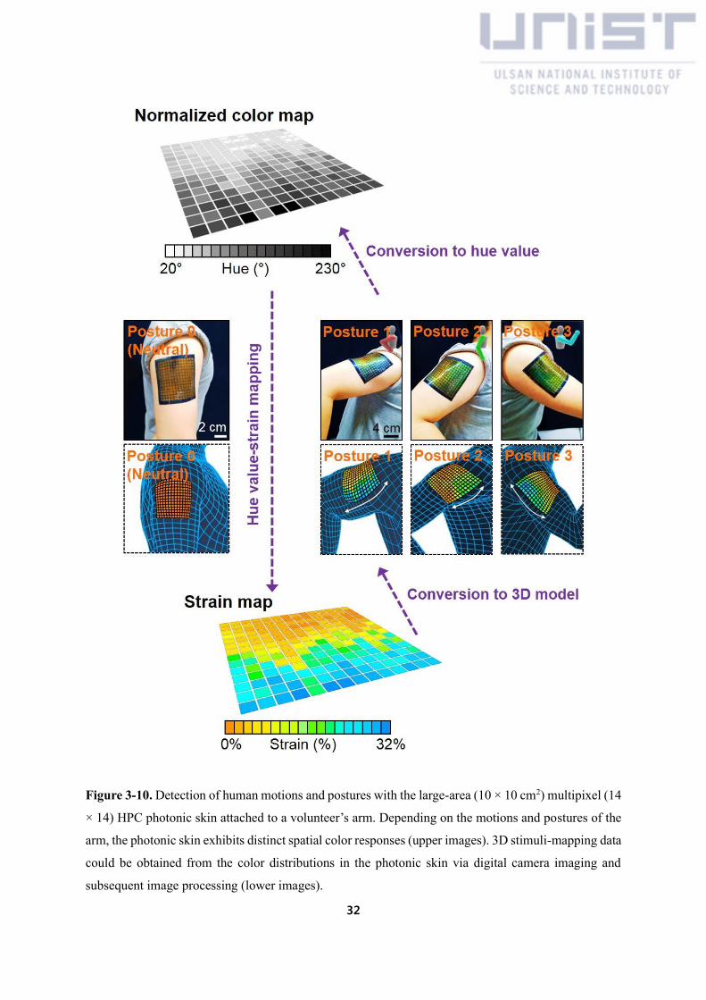
32
Figure 3-10. Detection of human motions and postures with the large-area (10 × 10 cm2) multipixel (14
× 14) HPC photonic skin attached to a volunteer’s arm. Depending on the motions and postures of the
arm, the photonic skin exhibits distinct spatial color responses (upper images). 3D stimuli-mapping data
could be obtained from the color distributions in the photonic skin via digital camera imaging and
subsequent image processing (lower images).

33
The attachable HPC photonic skin is also useful in the field of structural health monitoring, as it can
directly visualize any mode of structural failure. As a proof of concept application, the photonic skin
was attached to a PVC plate, followed by subsequent application of bending strain (Figure 3-11).
Without structural buckling, the skin exhibited a uniform red color across the array. Upon increasing
the degree of bending strain, the photonic skin showed obvious responsive coloration, with a peak shift
to shorter wavelengths. During the increase of the bending strain, the HPC skin maintained the
conformal attachment to the substrate without any delamination. In addition to the buckling and bending
of a plate, the photonic skin also could perceive the elongation of a model cable via the optical
transducing mechanism. As a final demonstration of conceptual application (Figure 3-12a), we applied
the photonic skin around diverse pipes (e.g., PVC, PE, and Al pipes) that deliver compressed air (Figure
3-12b). If there is any leakage due to puncture along the pipe, local pressure concentration would occur
at the site. The photonic skin conformably wrapping the pipe could directly detect the exact location of
the gas leakage through intuitive, immediate eye-readable coloration (Figure 3-12c). These results
confirm that the ultra-adaptable, multipixel HPC photonic skin suggested in this study has strong
potential as a wearable artificial skin with multiple characteristic functions of reversible ultra-
adaptability, spatio-temporal stimuli perception, and direct and intuitive stimuli visualization.

34
Figure 3-11. (a) Color responses of the photonic skin attached to a model plate under different bending
strains. (b) Color responses of the photonic skin attached to a model cable under different tensile strains.

35
Figure 3-12. Color responses of the photonic skin attached to gas pipes. The photonic skin can
immediately detect any leakage along the pipe via the intuitive color changes. (a) schematic illustration
showing the measurement of the pressure. (b) photonic skins attached to gas pipes. (c) color responses
of the photonics skin measuring the pressures.
3-3. Conclusion
Based on the wet-responsive HPC, ultra-adaptable and reusable bioinspired adhesives were
developed. Since it can be reliably attachable to highly rough substrates in response to a small amount
of water, these adaptable adhesives have in a variety of fields. Specifically, for wearable devices,
commercially available adhesives and existing bioinspired adhesives have shown several limitations,
but the developed adaptable adhesives were very suitable, because they are not only highly attachable
onto human skin but also reusable because of the shape-memory capability. With the advantages, a
novel wearable photonic skin with HPC multiplexed photonic sensors was developed, which can be
utilized for precise motion visualization of a human body or health monitoring of architecture. The
naturally abundant and eco-friendly cellulose-based photonic skin can firmly adhere to diverse
biological and non-biological target substrates and directly visualize various vital signals from the
substrates. We believe these wet-responsive adaptable adhesives can be a strong tool for development
of promising wearable devices.

36
3-4. Experimental Section
3-4-1. Fabrication of the wet-responsive adaptable HPC adhesive
To prepare the ultra-adaptable HPC adhesive, a low-concentration HPC (12 wt% in 0.1 wt% NaOH
solution) added with divinyl sulfone (0.42 wt%, Sigma Aldrich, USA) was casted on a master mold for
fabrication of the bioinspired adhesive structures. After drying at 25 °C for 24 h, the solidified HPC was
removed from the master mold, resulting in the HPC adhesive. The individual microstructure has a
cylindrical geometry with protruding tips. The stem diameter, tip diameter, and total height of the
microstructures are 20 μm, 26 μm, and 24 μm, respectively.
3-4-2. Surface analysis
Scanning electron microscope (SEM) images of the HPC microstructures were obtained with a S-
4800 microscope (Hitachi, Japan) after sputtering the microstructures with a 5-nm-thick Pt layer
(K575X sputter, Quorum Emitech, UK). The surface topographies of the various substrates were
measured using an Alpha-Step P-6 profiler (KLA-Tencor, USA). The root mean square roughness (RMS)
values were determined from the scanned images using Alpha-step imaging analysis software. To
evaluate the surface energies of the substrates, static contact angles of deionized water and glycerol
were measured on each substrate using a contact angle analyzer (SDLAB 200TEZD, Femtofab, Korea).
The measurements were repeated five times on each substrate and the averaged values were used. The
surface energies of the substrates were calculated by the geometric mean method.
3-4-3. Evaluation of adaptability and adhesion strength
Normal adhesion and peeling strengths of the HPC and PDMS adhesives were evaluated using
custom-built equipment (Figure 2-13). The equipment consisted of an automated movable part along a
vertical direction and a stage for fixing the samples. The movable part was connected to a load cell
(Ktoyo, Korea). For the measurements, target substrates were fixed on the mounting stage and adhesive
samples (area: 1 × 1 cm2) were mounted on the movable part with the adhesives facing down. Then,
the mounted adhesive samples were brought in contact with the substrates under a preload of 50 kPa.
Subsequently, an in-plane strain was applied along the vertical direction with a retraction speed of 1
mm s-1 until the separation occurred. For the peel tests, the adhesive samples were peeled at 180° angle
to the substrates. The adhesion performance of the swollen HPC adhesives was evaluated by hydrating
the HPC adhesives in a closed humid chamber (relative humidity: 95%, temperature: 30 °C) for 180 s.
The hydrated HPC adhesives were brought into contact with the substrates under a preload of 50 kPa
for 100 s at room temperature (25 °C), during which the HPC adhesives were dehydrated. For each of

37
the PDMS, pristine HPC, and swollen HPC adhesives, five different samples were prepared for the
adhesion tests; adhesion measurements of each sample were repeated five times and the averaged values
were reported.
3-4-4. Fabrication of wearable photonic skin
The multipixel photonic skin consists of an encapsulation film, active HPC photonic layer, pixelated
chamber, CNT composite electronic sensor, and HPC adhesive. To prepare the pixelated HPC photonic
sensor, a pixelated chamber was first prepared by replicating an aluminum master mold with grid
patterns using a PDMS base polymer (Sylgard 184, Dow Corning Korea, Korea) mixed with black dye
(Cannon, Japan) and curing agent (10 wt%). the high-concentration HPC (MW: 100,000, Alfa Aesar,
USA) was prepared by centrifuging 60 wt% HPC in deionized water. Then, the centrifuged HPC was
filled into the prepared PDMS grid chamber, followed by removing the excess HPC using a doctor
blade. After relaxation for 12 h, the filled HPC started to exhibit iridescent colors based on the self-
assembly of the HPC into the cholesteric phase. Subsequently, the PDMS grid chamber filled with the
HPC was encapsulated with an O2-plasma-treated PDMS sheet (thickness: 50 μm) using a press
machine. The HPC photonic sensor and HPC adhesive layer were then covalently laminated to each
other via O2 plasma treatment. To prepare the CNT composite electronic sensor, a MWCNT-PDMS
mixture was first prepared by dispersing MWCNTs (diameter: 4 nm, length: 70-80 µm, CM250,
Hanhwa Chemical, Korea) in chloroform by sonication for 50 min. Then, the MWCNT-dispersed
solution was mixed with a PDMS base polymer at a concentration of 2 wt%, followed by evaporation
of the chloroform on a hot plate at 100 °C for 6 h. The MWCNT-PDMS mixture, with the addition of a
10 wt% PDMS curing agent, was drop-casted on a flat Si wafer, followed by pressing using a press
machine and thermal curing at 70 °C for 1 h. Subsequent removal from the press machine resulted in
the MWCNT-composite-based, thin-film e-skin (thickness: 50 µm). Copper electrodes were generated
on the upper and bottom surfaces of the MWCNT e-skin via electron-beam evaporation for the
multiplexed force measurement. The MWCNT e-skin was inserted between the HPC photonic sensor
layer and the HPC adhesive layer upon requirements.
3-4-5 Characterization of the mechanochromic behavior of the photonic skin
Color distributions of the multipixel photonic skin under controlled pressures or tensile strains were
imaged with a digital camera. Then, the HSV values and RGB values of each pixel were extracted using
an image analysis software.

38
Chapter 4. Wet-responsive switchable Adhesive
This chapter includes the published contents:
H. Yi, M. Seong, K. Sun, I. Hwang, K. Lee, C. Cha, T. Kim, and H. E. Jeong, Adv. Funct. Mat., 2019,
1706498. Copyright © 2018 Wiley.
4-1. Introduction
Nanotransfer printing (nTP) is one of the most promising nanofabrication techniques for the
development of flexible electronic, optical, and biomedical devices as it enables the formation of
functional nanomembranes and materials on a wide range of unconventional substrates such as flexible
plastics, non-planar surfaces, and even biological tissues. 12, 16, 74-80 Transfer printing typically consists
of three main steps: (1) preparation of micro- or nanoscale membranes on a donor substrate, (2) transfer
of the membranes from the donor substrate to a stamp, and (3) transfer of the membranes on the stamp
to a receiver substrate. It is possible for micro or nanomembranes to be directly formed on the stamp
without the first step of donor-stamp transfer. Regardless of the methodology, precise adhesion control
at the interfaces between the nanomembranes, stamp, donor, and receiver substrates is of great
importance for a successful and reliable transfer.
Many different types of nTP techniques have been developed to date, in which adhesion is controlled
by different methods including kinetic adhesion control,24-33 direct use of adhesive tape,81 coating of
chemicals or self-assembled monolayers (SAMs),28, 82-84 surface oxidation,85-86 solvent-assisted
adhesion control,87 and selective removal of sacrificial layers.84, 88-90 While these methods are efficient
and useful for nTP, several challenges still remain. For example, many of previous approaches require
surface coatings or treatments with ancillary chemicals or adhesive materials, which are only necessary
for the nTP process and unnecessary for the functions of the final devices, even impeding device
performance. Furthermore, the surface energy of the coating materials is fixed and not controllable on
demand. Different coating materials with varying surface energies are required depending on the type
of nanomembranes, stamps, and substrates. Furthermore, nTP methods utilizing solvents or harsh
etchants for the selective removal of sacrificial or specific layers often result in deformations and
damage to the stamps, nanomaterials, and final devices.
Adhesives that can actively and precisely control the adhesion on demand could be an effective
solution to address the aforementioned challenges. Commercially available thermal release tape is an
adhesive whose properties can be controlled by changes in temperature.16, 91 However, this requires an

39
external energy input to cause a temperature increase, and a chemical adhesive layer, which could leave
residues on the contacting surfaces. Recently, microstructured smart adhesives with reversible,
controllable, and switchable adhesion properties have demonstrated their usefulness for potential
application in nTP. However, investigations into smart adhesives that exhibit strong, actively
controllable, and switchable adhesion in response to external stimuli are still required for further
developments.10, 92-93
In this chapter, we present wet-responsive and biocompatible smart hydrogel adhesives that exhibit
actively controllable, switchable, and reversible adhesion based on wet-responsive nano/microscopic
and macroscopic shape reconfigurations of PEGDMA hydrogel. The developed smart hydrogel
adhesive exhibits excellent adhesion strength (as high as ~191 kPa) with the aid of nano- or
microstructured arrays on the substrate surface in the dry state. When the adhesive is exposed to water,
a hydration-induced shape transformation of the array and macroscopic film bending takes place,
switching the adhesion off (~0.30 kPa) with an extremely high adhesion switching ratio (>640). The
adhesives also exhibit good repeatability and durability, maintaining their smart adhesion behaviors
over repeated cycles of hydration and dehydration. Furthermore, the thin (~2–200 μm) and flexible
features of the adhesive film facilitate a conformal and firm contact with diverse planar and curved
surfaces. With these smart adhesion properties, the reconfigurable hydrogel adhesives enable transfer
printing of a wide range of semiconducting and metallic nanomembranes on diverse substrates such as
flexible polyethylene terephthalate (PET) film, rigid Si wafer, and curved glass cylinder, requiring only
water and without the need for an external energy input, toxic solvents, or chemicals. The smart
hydrogel adhesives are useful for the nTP onto delicate biological substrates such as skin, tissues, and
organs as they are made of biocompatible hydrogels and their adhesion-on/off is modulated with water.
To demonstrate the useful application of the prepared hydrogel adhesive, we have shown that the wet-
responsive and reconfigurable hydrogels can be used for the transfer printing of a nanocrack-based
strain sensor onto a bovine eye.94-95 The transferred strain sensor successfully detects intraocular (IOP)
pressure with high sensitivity and reversibility. The results presented herein show the versatility and
potential of the wet-responsive and reconfigurable adhesive for the transfer printing of diverse
nanoscale and microscale materials on a wide range of substrates.
4-2. Results and Discussion
4-2-1. Swelling behaviors of wet-responsive PEDGMA adhesives

40
Figure 1a shows the wet-responsive and reconfigurable PEGDMA adhesive fabricated with a replica
molding technique utilizing PEGDMA as a base material (Figure 4-1a). PEGDMA is a hydrogel capable
of absorbing large amounts of water and can be cured by exposure to ultraviolet (UV) light, which
enables an easy and reliable fabrication of micro- or nanoscale structures. 96-98 The fabricated PEGDMA
adhesives are thin flexible films with nano- or microstructural arrays on their surface (Figure 4-1b, c
and d). Here, we used three different kinds of arrays with stem diameters (Ds: ~400 nm, 5 μm, and 20
μm). All arrays had a spacing ratio of 1. The arrays of the adhesive were designed to have protruding
tips on the cylindrical stem (bioinspired mushroom-shaped pillars). These structural features produced
exhibit strong adhesion on arbitrary surfaces by van der Waals interaction to the PEGDMA adhesive.
Thus, our switchable adhesives intrinsically exhibit strong, residue-free, and reversible adhesion with
various surfaces of nanomembranes and substrates. When the crosslinked PEGDMA structures are
exposed to water, the water is entrapped in the 3D hydrogel networks, resulting in a significant volume
expansion (Figure 4-1e).99-100
Figure 4-1. (a) Schematic of the fabrication of the wet-responsive PEGDMA adhesives. Photo and SEM
images of the fabricated the adhesives: (b) Ds: 400 nm, (c) Ds: 5 μm and (d) Ds: 20 μm. (e) Conceptual
illustration of the reversible hydration and dehydration process of the PEGDMA bioinspired structure.

41
Consequently, the hydrogel arrays are swollen with a noticeable increase in the structural diameter
and height. The changes in PEGDMA nano- or microstructures before and after swelling are shown in
Figure 1b. To visualize the wet-responsive swelling, PEGDMA with a high MW of ~6,000 was utilized
because hydrogels with higher MWs undergo a more drastic volume expansion upon swelling. As can
be seen, the swollen PEGDMA had more expanded and porous structures compared to the dried
PEGDMA. For fabrication of the PEGDMA adhesives, we utilized PEGDMA with MW of 750. This
hydration-induced shape reconfiguration is reversible, and the expanded structure can recover its
original shape and size upon the evaporation of water.
Details of the microscopic swelling behaviors of the PEGDMA adhesives were analyzed with the
microstructure arrays (Ds 20 μm). The swelling behaviors of the PEGDMA adhesives were numerically
evaluated based on the swelling ratio (%) defined as W/Wi, where W is the weight of the swollen
adhesives at specific times and Wi is the original weight of the bioinspired adhesives. The original
weight (Wi) of the adhesives corresponded to the constant weight during the vacuum-drying of the
adhesive. Figures 4-2a and b show the time-lapse optical microscopy images showing the shape
transformations of the microstructures made of 80% PEGMDA (80 wt% PEGDMA and 20 wt% water)
in response to water. The tip diameter of the microstructures gradually increased as the structures
swollen by water. The original diameter of 24.3 μm gradually increased to 28.4, 29.5, and 30.6 μm after
30, 60, and 180 s of swelling, respectively. The structural height also increased from the original height
of 20.4 μm to 27.2 μm after 180 s of swelling. Upon drying, the increased diameter and height began to
decrease, and the structures recovered its original size, proving the reversibility of the microscopic
shape change of the hydrogel microstructures (Figure 4-2a, b). During the analysis, the adhesives was
dried on a hot plate (30 ℃). Changes in the diameters and heights as a function of water exposure time
are shown in Figures 4-3a–d for the two different arrays (microstructures with a 24.3 μm tip diameter
and 20.4 μm height, and microstructures with a 7.4 μm tip diameter and 5.1 μm height). Size changes
of the nanostructure array (Ds: 400 nm) could not be measured because of the limited resolution of the
optical microscope. As shown, the size of the microstructures drastically increased after 30 s of swelling,
sequentially the growth rate started to decrease.

42
Figure 4-2. (a) Optical microscopy images showing the top views of the PEGDMA microstructure
(initial tip diameter: 24.3 μm, initial stem diameter: 20 μm, initial height: 20.4 μm) during the hydration
and dehydration process. Dehydration was achieved by heating on a hot plate (30 °C). (b) Optical
microscopy images showing the side views of the PEGDMA microstructure during the hydration and
dehydration processes.

43
Figure 4-3. (a) Tip diameter and (b) height of the PEGDMA microstructures with 20 and 5 μm stem
diameters as a function of swelling time. Ratios of variations in the (c) tip diameter and (d) height of
the microstructures as a function of swelling time.
Figure 4-4a shows the time-lapse images of the macroscopic shape transformation of the PEGDMA
adhesive (80 wt% PEGDMA/50-μm-thick PET film). As the water started to penetrate the
adhesive/substrate interface and was absorbed by the PEGDMA adhesive, macroscopic film bending
occurred because the PEGDMA layer of the adhesive expanded in volume while the supporting PET
layer maintained its original shape and size. This hydration-induced film bending was fully reversible,
as demonstrated in Figure 4-4a. Upon deswelling of the adhesive by water evaporation, the folded film
recovered to its original shape. Interestingly, the flattened adhesive attached to the substrate through
van der Waal force-based adhesion without the application of external loads.
The degree of adhesive film bending can be controlled by using PET films with different thicknesses
(Figures 4-4b, c and d). When a thick (~250 μm) PET film was used as a supporting layer for the
adhesive, slight bending with a bending radius of curvature of 143 mm after 1 min was observed.
Bending radii of 6.8 and 1.0 mm were observed for the PET films with thicknesses of ~125 and ~50

44
μm, respectively. When ~2-μm-thick PET films were used, the adhesive became rolled up, as shown in
Figure 4-4d. The degree of film bending could also be controlled using PEGDMA with different
concentrations (Figure 4-4e). Figure 3-4 f shows the radius of curvature of the adhesives made from
different concentrations of PEGDMA on a PET film with thickness of 50 μm after 1 min of swelling.
The PEGDMA adhesives made from lower concentrations of PEGDMA exhibited smaller bending
radius as they underwent higher volume expansions in the presence of water. In contrast to the
PEGDMA adhesive, the PDMS adhesive was unchanged by the presence of water.
Figure 4-4. (a) Time-lapse photography showing the hydration-induced spontaneous bending of the
PEGDMA adhesive film and reflattening of the adhesive during dehydration at 30 °C. Hydration-
induced bending of the PEGDMA adhesives with different PET thicknesses: (b) 125 μm PET, (c) 50
μm PET and (d) 2 μm PET. (e) Radius of curvature of the adhesive film as a function of PET film
thickness. (f) Radius of curvature of the adhesives made from different concentrations of PEGDMA on
50-μm-thick PET films.

45
4-2-2. Wet-responsive switchable adhesion property of the adhesive
The wet-responsive swelling behaviors of the adhesives result in that wet-responsive and active
detachment of the adhesives. At the dry state, the adhesives can exhibit strong adhesion onto diverse
substrates by van der Waals interaction. However, as the water droplet penetrates the gap between the
PEGDMA adhesive and the substrate through capillary action, the PEGDMA adhesive starts to swell
(Figure 4-5 and 6). The swelling of the PEGDMA adhesive induces the macroscopic folding and
bending of the adhesive film and results in nano- or microscopic volume expansion, and subsequent
shape transformation of the structure array (Figure 4-5). These water-induced macroscopic and
nano/microscopic reconfiguration of the PEGDMA adhesive enable the adhesive a reversible, active
and switchable adhesion property.
Figure 4-5. (a) Tip diameter and (b) height of the PEGDMA microstructures with 20 and 5 μm stem
diameters as a function of swelling time. Ratios of variations in the (c) tip diameter and (d) height of
the microstructures as a function of swelling time.
Figure 4-6 shows the direct observations of the overall detachment process of the switchable adhesive
placed on a glass substrate. For visualization, adhesives with microscale arrays (stem diameter: ~20 μm,
height: ~22 μm) were utilized. As the water penetrated the gap between the attached adhesive and

46
substrate, one end of the tip of microstructures wetted by the water started to detach from the substrate
because the van der Waals interactions between the swollen, hydrated surface of the microstructures
and the substrate decreased. 101 Simultaneously, the switchable adhesive film started bending because
of the mismatch in volume expansion between the hydrogel layer and the supporting PET film.
Consequently, a crack propagated along the direction of water penetration, resulting in sequential
detachment of the PEGDMA adhesive from the substrate (Figure 4-6a).
Figure 4-6. Optical microscope images showing the spontaneous detachment process of the adhesive
attached to a glass substrate by the reconfigurations of the adhesive film structure in response to water
penetration.

47
As seen in Figure 4-7, the adhesion switchability of the adhesives showed a highly switchable
adhesion. In adhesion-on state, with such a strong adhesion strength, the hydrogel adhesive could hold
a significant weight (6 kg dumbbell) and could not easily detach from a substrate once adhered to a
rigid substrate such as a glass. However, it could be easily detached on demand by dropping water on
the adhesive, showing very low adhesion strength.
Figure 4-7. (a) Photographs of the PEGDMA adhesives bearing a significant weight of 6 kg dumbbell
for a long period of time in the dry state. (b) Conceptual illustration showing the components for the
hanging of loads to the PEGDMA adhesive. (c) Time-lapse photography showing the detachment of the
PEGDMA adhesive holding a weight of 100 g in response to water penetration. In contact with water,
the PEGDMA adhesive lost the adhesion within 30 s.
4-2-3. Adhesion measurements of the adhesives
The adhesion measurements of the PEGDMA adhesive was examined by using the custom-built
equipment. Figure 4-8a shows the measured adhesion strength of the PEGDMA adhesive (80wt%
PEGDMA with MW of 750) as a function of preload and depending on the geometries of the array on
the adhesive surface. PEGDMA adhesives with 400 nm arrays exhibited a pull-off strength of ~114 kPa

48
at a low preload of ~5 kPa. With increasing preload, the pull-off strength monotonically increased and
reached ~191 kPa for preloads of 50 kPa. Adhesives with microscale arrays showed generally decreased
adhesion strengths. This is because structures with smaller diameters and higher densities could produce
larger contacts against a substrate. Furthermore, as the diameter became smaller, the effective moduli
of the structures become lower, which facilitated the conformal contacts against a substrate under a low
preload. In addition, structures with smaller diameters become less sensitive to defects on a substrate.
102-104 Nonetheless, adhesives with microstructure array still exhibited high adhesion strength with
similar adhesion behavior as the nanostructure arrays (Figure 4-8). In contrast, the nonpatterned
hydrogel surfaces exhibited significantly low pull-off strengths (< ~10 kPa) than those of the adhesives
with patterned arrays over entire ranges of preloads (Figure4-8a and b). This result demonstrated that
our switchable adhesives with micro- or nanostructure arrays are highly useful to obtain high adhesion
strengths and adhesion switching ratio.
To further investigate the adhesion behavior of the PEGDMA adhesives, adhesion measurements
were carried out for switchable adhesives with two different molecular weights (MW 750 and 550) and
three different concentrations in water (PEGDMA wt%: 100, 90, and 80) (Table 4-1). Based on the
measurement results of their mechanical properties, hydrogel samples with higher MWs and higher
water contents depicted lower mechanical strengths (Table 4-2 and Figure 4-9). Figures 4-8b and c show
the adhesions of the planar and microstructured hydrogel samples as functions of MWs and
concentrations. As shown, the adhesion of the PEGDMA surfaces varied depending on their mechanical
strengths. PEGDMA adhesives with the lower elastic modulus (MW: 750) exhibited notably higher
adhesion strengths than those of the samples with the higher elastic modulus (MW: 550) because the
former adhesives made more conformal contacts against a substrate under the same preload. For the
adhesives with the same MWs, samples with higher hydrogel contents showed a slightly higher elastic
modulus than those with lower hydrogel concentrations. However, such small differences in the
PEGDMA concentrations (100, 90, and 80 wt%) did not induce any noticeable difference in the
resulting adhesions (Figures 4-8b, c).

49
Figure 4-8. (a) Tip diameter and (b) height of the PEGDMA microstructures with 20 and 5 μm stem
diameters as a function of swelling time. Ratios of variations in the (c) tip diameter and (d) height of
the microstructures as a function of swelling time.

50
Table 4-1. Formulations of various PEGDMA solutions.
Hydrogel
Precursor
PEGDMA
MW: 750 (wt%)
PEGDMA
MW: 550 (wt%)
Distilled water
(wt%)
Irgacure
2959 (wt%)
750 / 80% 80 20 0.2
750 / 90% 90 10 0.2
750 / 100% 100 0 0.2
550 / 80%
80 20 0.2
550 / 90%
90 10 0.2
550 / 100%
100 0 0.2
Table 4-2. Mechanical properties of PEGDMA having different molecular weights and concentrations.
PEGDMA
(MW / wt%)
Elastic modulus
(MPa)
Elongation at break
(%)
750 / 80 15.5 3.3 47.4 4.6
750 / 90 16.7 3.4 40.7 3.1
750 / 100 18.7 3.7 33.2 2.2
550 / 80 39.4 4.6 18.8 1.9
550 / 90 46.2 5.2 15.4 1.4
550 / 100 49.3 5.9 11.2 1.1
Figure 4-9. Tensile stress-strain curves of PEGDMA with MW of 750 and 550 of various concentrations.

51
In order to demonstrate the strong, water-responsive, and switchable adhesion capability, we
measured the adhesion strengths during repeated cycles of the adhesion-on/off (dehydration/hydration)
(Figure 4-10). During the repeated cycles of swelling and deswelling, the switchable adhesives
exhibited high adhesion strengths in the dry state and nearly zero adhesion (0.19–0.34 kPa) in the
swollen state, in a reversible and stable manner. These results indicate that our wet-responsive
reconfigurable adhesives have superior and smart adhesion capabilities, including active adhesion
controllability, switchability, reversibility, and durability.
Figure 4-10. Adhesion strengths of the PEGDMA adhesives with different stem diameters during
repeated swelling and deswelling cycles. For the durability tests, PEGDMA adhesives were swollen
with water for 30 s followed by drying on a hot plate (30 °C).
4-2-4. Application of the adhesive 1: Nanotransfer printing
With the smart switchable adhesion of the adhesives, nanomembranes could be transferred from the
adhesive surface onto the receiver substrates in a simple and spontaneous manner. Figure 4-11a shows
the overall procedure of transfer printing of the nanomembranes using the switchable adhesive. In the
first step, the switchable adhesive with nanostructure array is brought into contact with the

52
nanomembranes formed on a donor substrate. Sequentially, the nanomembranes are transferred from
the donor substrate to the adhesive surface by the strong adhesion strength at adhesion-on state. The
adhesion strength can be controlled by the modulation of the geometry of the hydrogel nanostructures
(e.g., diameter, height, tip shape, and structural density). Next, the switchable adhesive with attached
membranes is conformably placed on a receiver substrate, followed by the dropping of water on one
side of the attached adhesive film. The dropped water can penetrate the interface between the membrane
and the substrate. In this case, the water acts as an adhesive layer between the membranes and receiver
substrate, enabling strong attachment of the membrane to the substrate after the water dries. 101 . After
the water evaporation, the adhesives are detached, leaving the membranes onto the receiver substrate.
Figure 4-11. (a) Conceptual illustration of the transfer printing of nanomembranes using the wet-
responsive PEGDMA adhesives. (b) Transfer printing of a patterned Au membrane (thickness: 400 nm)
from the donor substrate (Si wafer) to the receiver substrate (glass) using the wet-responsive and
reconfigurable PEGDMA adhesive. Upon contact with water, the patterned Au membrane on the surface
of the PEGDMA adhesive could be smoothly released from the adhesive surface by the hydration-
triggered spontaneous macroscopic film bending and nano/microscopic shape transformations of the
adhesive array. Inset in (viii) is a surface profile image measured by AFM that shows the thickness of
the Au membrane.
In order to optimize the nTP technique with PEGDMA adhesives, we used three different kinds of
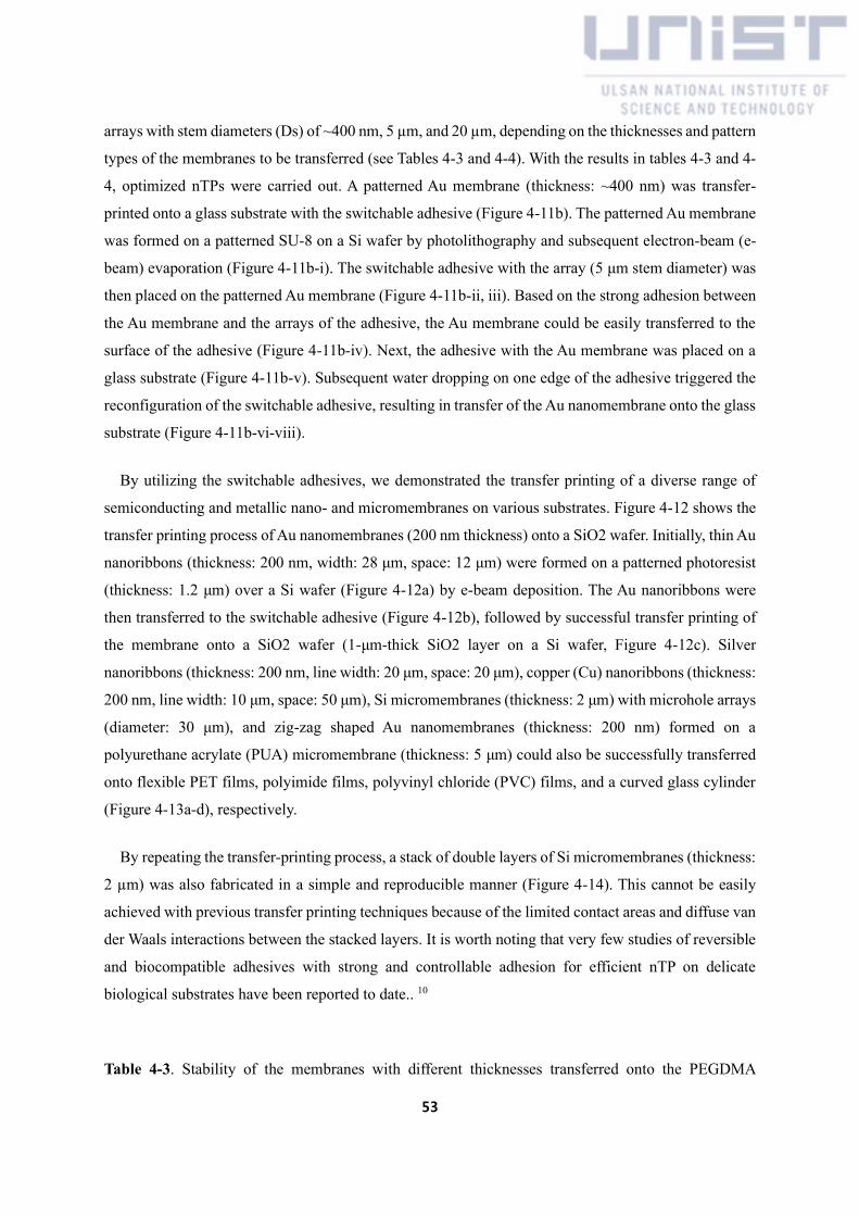
53
arrays with stem diameters (Ds) of ~400 nm, 5 µm, and 20 µm, depending on the thicknesses and pattern
types of the membranes to be transferred (see Tables 4-3 and 4-4). With the results in tables 4-3 and 4-
4, optimized nTPs were carried out. A patterned Au membrane (thickness: ~400 nm) was transfer-
printed onto a glass substrate with the switchable adhesive (Figure 4-11b). The patterned Au membrane
was formed on a patterned SU-8 on a Si wafer by photolithography and subsequent electron-beam (e-
beam) evaporation (Figure 4-11b-i). The switchable adhesive with the array (5 μm stem diameter) was
then placed on the patterned Au membrane (Figure 4-11b-ii, iii). Based on the strong adhesion between
the Au membrane and the arrays of the adhesive, the Au membrane could be easily transferred to the
surface of the adhesive (Figure 4-11b-iv). Next, the adhesive with the Au membrane was placed on a
glass substrate (Figure 4-11b-v). Subsequent water dropping on one edge of the adhesive triggered the
reconfiguration of the switchable adhesive, resulting in transfer of the Au nanomembrane onto the glass
substrate (Figure 4-11b-vi-viii).
By utilizing the switchable adhesives, we demonstrated the transfer printing of a diverse range of
semiconducting and metallic nano- and micromembranes on various substrates. Figure 4-12 shows the
transfer printing process of Au nanomembranes (200 nm thickness) onto a SiO2 wafer. Initially, thin Au
nanoribbons (thickness: 200 nm, width: 28 μm, space: 12 μm) were formed on a patterned photoresist
(thickness: 1.2 μm) over a Si wafer (Figure 4-12a) by e-beam deposition. The Au nanoribbons were
then transferred to the switchable adhesive (Figure 4-12b), followed by successful transfer printing of
the membrane onto a SiO2 wafer (1-μm-thick SiO2 layer on a Si wafer, Figure 4-12c). Silver
nanoribbons (thickness: 200 nm, line width: 20 μm, space: 20 μm), copper (Cu) nanoribbons (thickness:
200 nm, line width: 10 μm, space: 50 μm), Si micromembranes (thickness: 2 μm) with microhole arrays
(diameter: 30 μm), and zig-zag shaped Au nanomembranes (thickness: 200 nm) formed on a
polyurethane acrylate (PUA) micromembrane (thickness: 5 μm) could also be successfully transferred
onto flexible PET films, polyimide films, polyvinyl chloride (PVC) films, and a curved glass cylinder
(Figure 4-13a-d), respectively.
By repeating the transfer-printing process, a stack of double layers of Si micromembranes (thickness:
2 µm) was also fabricated in a simple and reproducible manner (Figure 4-14). This cannot be easily
achieved with previous transfer printing techniques because of the limited contact areas and diffuse van
der Waals interactions between the stacked layers. It is worth noting that very few studies of reversible
and biocompatible adhesives with strong and controllable adhesion for efficient nTP on delicate
biological substrates have been reported to date.. 10
Table 4-3. Stability of the membranes with different thicknesses transferred onto the PEGDMA

54
adhesives with different stem diameters (Ds) of 400 nm, 5 µm, and 20 µm.
Thin-film type membranes Ds : 400 nm Ds : 5 μm Ds : 20 μm
Si
membrane
thickness: 200 nm
thickness: 500 nm
thickness: 2 μm
Ag
membrane
thickness: 200 nm
thickness: 500 nm
thickness: 2 μm
Au
membrane
thickness: 200 nm
thickness: 500 nm
thickness: 2 μm
Membrane
Array
Membrane
Array
Membrane
Array

55
Table 4-4. Stability of the ribbon-type membranes with different thicknesses transferred onto the
PEGDMA adhesives with different stem diameters (Ds) of 400 nm, 5 µm, and 20 µm.
Ribbon-type membranes Ds : 400 nm Ds : 5 μm Ds : 20 μm
Si ribbon-
type
membrane
thickness: 200 nm
thickness: 500 nm
thickness: 2 μm
Ag ribbon-
type
membrane
thickness: 200 nm
thickness: 500 nm
thickness: 2 μm
Au ribbon-
type
membrane
thickness: 200 nm
thickness: 500 nm
thickness: 2 μm
Wrinkled

56
Figure 4-12. Optical microscopy and AFM images showing the transfer printing process of Au
nanoribbons (thickness: 200 nm, width: 28 µm, space: 12 µm) from an Si wafer to an SiO2 wafer (1-
µm-thick SiO2 layer on Si wafer) via the PEGDMA adhesive. AFM images show the top- and cross-
sectional views of the Au membrane before and after transfer printing. Before transfer printing, the Au
nanoribbons were formed on a patterned photoresist (thickness: 1.2 µm)

57
Figure 4-13. (a) Ag nanoribbons (thickness: 200 nm, line width: 20 µm, space: 20 µm) transferred onto
a PET film. (b) Cu nanoribbons (thickness: 200 nm, line width: 10 µm, space: 50 µm) transferred onto
a polyimide film. (c) Si micromembranes (thickness: 2 µm) with microhole arrays (diameter: 30 µm)
formed on a PVC film. (d) Zig-zag shaped Au (thickness: 200 nm)-PUA (thickness: 5 µm) composite
membranes transferred onto a curved glass cylinder.
Figure 4-14. SEM images of the double stacked Si line patterns formed by utilizing the PEGDMA
adhesives.
For further demonstration of applicability, we fabricated Si nanoribbon transistors on a SiO2/Si
substrate (Figure 4-15). The Si nanoribbons were transfer-printed onto an SiO2/Si wafer (SiO2 thickness
of 100 nm) based on the nTP with PEGDMA adhesives, followed by electrode formation (100 nm Au)
utilizing e-beam evaporation. The resulting Si nanomembrane transistor exhibited I–V curves that were
identical to the curves measured from the Si transistor directly fabricated by the conventional
photolithographic process, which demonstrated the validity of our approach.

58
Figure 4-15. (a) Conceptual illustration of the Si nanoribbon transistor fabricated on a SiO2/Si substrate
based on nTP with the hydrogel adhesives. (b) SEM image, (c) VGS-IDS curve, and (d) IDS-VDS curve
of the Si nanomembrane FET transistor fabricated by the conventional photolithographic process. (e)
SEM image, (f) VGS-IDS curve, and (g) IDS-VDS curve of the Si nanomembrane FET transistor
fabricated by nTP with PEGDMA adhesives.
It is worth noting that very few studies of reversible and biocompatible adhesives with strong and
controllable adhesion for efficient nTP on delicate biological substrates have been reported to date. The
PEGDMA adhesive is a possible solution to the transfer printing of functional nanomembranes onto
biological surfaces because it is made of a biocompatible hydrogel, and its adhesion can be controlled
with only water or physiological solutions. Figure 4-16a shows Ag nanomembranes with 200 nm
thickness (line width: 25 µm, spacing: 120 µm) transferred onto a plant leaf. The transfer printing of
Pt/SU-8 composite membranes (Pt thickness: 50 nm, SU-8 thickness: 400 nm) onto human skin was
also achieved with the adhesive (Figure 4-16b). Furthermore, Au/SU-8 (Au thickness: 100 nm, SU-8
thickness: 400 nm) membranes could be transferred onto a porcine heart using the hydrogel adhesives
(Figure 4-16c).

59
Figure 4-16. (a) Ag nanoribbons (thickness: 200 nm, line width: 25 µm, space: 120 µm) transferred
onto a plant leaf. (b) Pt (thickness: 50 nm)-SU-8 (thickness: 400 nm) composite membranes transferred
onto human skin. The transferred membrane was firmly attached to the skin during both (i) tension and
(ii) compression of the skin. (c) Au (thickness: 100 nm)-SU-8 (thickness: 400 nm) composite
membranes transferred onto a porcine heart.
4-2-5. Application of the adhesive 2: Transfer printing of nanocrack sensor onto bovine eye
Based on the nTP process utilizing the PEGDMA adhesives, we transferred a strain sensor based on
nanocrack onto a bovine eye for the measurement of the intraocular pressure (IOP). IOP is an important
indicator to evaluate patients at risk of glaucoma.[64] To measure the IOP of the eye, we prepared a
honeycomb-shaped strain sensor based on nanocrack by photolithography and e-beam deposition for
the metal layer. (Figure 4-17a). The sensor consisted of a platinum (Pt) nanomembrane (20 nm thick)
and base SU-8 micromembrane (2 µm thick). (Figure 4-17 d). Nanocracks were fabricated in the Pt
membrane by applying a bending stress. 94-95 The fabricated sensor had nanocracks (100 nm width and
35 nm depth) in the transverse direction to the extension force (Figure 4-17b and d). The nanocrack
sensor fabricated on the silicon donor substrate was stably transferred onto the curved bovine eye from
the adhesive with a drop of saline solution, showing the switchable adhesion and biocompatibility of
the adhesives (Figure 4-17a, c, e). The transferred sensor could measure the IOP based on the resistance
change produced from the strain changes of the cracked Pt membrane in response to the IOP (Figure 4-

60
17c and e). Figure 4-18a shows the resistance during repeating loading and unloading of the bovine eye
to an IOP of 40 mmHg. Figure 4-18b shows the resistance variations measured during the loading and
unloading of different IOPs (sweeping speed: 0.4 mmHg/s). The transferred sensor could measure the
variations of the IOPs with high sensitivity. (Figure 4-18c).
Figure 4-17. (a) Schematic illustration of the fabrication of the nanoscale crack sensor and its
subsequent transfer printing onto a bovine eye using the PEGDMA adhesive with saline solution. (b)
Conceptual illustration of the nanocrack sensor in which nanoscale cracks were formed in the Pt layer
(thickness: 20 nm) coated on the SU-8 layer (thickness: 2 µm). (c) Conceptual illustration of the
detection of the IOP using the sensor (d) Photograph of the fabricated nanocrack sensor. AFM images
on the right show the morphology of the nanocrack. The nanocracks have an average width of ≈100 nm
and depth of ≈35 nm. (e) Photograph of the nanocrack sensor transferred onto a bovine eye.

61
Figure 4-18. (a) Normalized resistance variations measured with the transferred nanocrack sensor
during repetitive cycles of loading and unloading of pressure (40 mmHg). (b) Normalized resistance
variations showing the reversible loading–unloading behaviors at different pressures (10, 20, 30, and
40 mmHg). (c) Normalized resistance variations during loading and unloading as a function of the IOP.

62
4-3. Conclusion
We have developed a smart PEGDMA hydrogel adhesive that enables actively-controllable and
switchable adhesions based on the wet-triggered nano/microscopic and macroscopic shape
transformation of the adhesive films. The PEGDMA adhesives showed a high adhesion strength of
~191 kPa in the dry state and nearly zero adhesion (~0.30 kPa) in the swollen state. With repeated cycles
of swelling and deswelling, the hydrogel adhesives maintained their controllable and switchable
adhesion capabilities without any notable degradation. We demonstrated that this water-responsive and
reconfigurable hydrogel adhesive can be used for the transfer printing of diverse metallic (Au, Ag, Cu,
and Pt) and semiconducting (Si) membranes onto arbitrary surfaces such as flexible plastic films, rigid
Si wafers, curved glass cylinders, and even biological tissues using only water. Furthermore, we showed
that the wet-responsive and reconfigurable adhesives could be used for the transfer printing of a
nanocrack-based strain sensor onto a bovine eye. The transferred nanocrack sensor successfully
detected the IOP with high sensitivity, repeatability, and reversibility. We believe this stimuli-
responsive and shape-transformable hydrogel adhesive could serve as a versatile smart adhesive for the
transfer printing of a diverse range of nanoscale architectures on many different surfaces.
4-4. Experimental Section
4-4-1. Fabrication of the wet-responsive switchable PEGDMA adhesives
PEGDMA solutions with 0.2 wt% of the photoinitiator (Irgacure 2959, Sigma Aldrich) were
deposited onto the master for the fabrication of bioinspired adhesive structures and PET film was placed
onto the deposited PEGDMA solution. PEGDMA solutions of different concentrations were prepared
by mixing PEGDMA (Sigma Aldrich) with DI water at different ratios (PEGDMA wt%: 100, 90, 80,
and 70 wt%). The PEGDMA solutions were crosslinked by UV exposure (λ = 365 nm, dose = 300 mJ
cm−2) and demolded from the master, which produced PEGDMA adhesives with mushroom-shaped
micropillar arrays. The fabricated PEGDMA adhesives were exposed to UV radiation for 6 hours. The
samples were dried at the vacuum condition of 30 °C for the complete dehydration.
4-4-2. Visualization of the PEGDMA microstructures before and after swelling
PEGDMA adhesives were prepared by using 10% PEGDMA (10 wt% MW 6000 PEGDMA mixed
with 90 wt% DI water and 0.2 wt% irgacure 2959). The 10% PEGDMA solutions were dispensed onto
the PDMS mold followed by the placement of a PET film onto the PEGDMA. Subsequent UV exposure

63
(dose: 300 mJ cm–2) resulted in the desired PEGDMA film. The film was dried at a vacuum condition
for SEM imaging of the microstructures of dried PEGDMA. For imaging of the microstructures of
swollen PEGDMA, the film was swollen in DI water for 24 hours. And then, the sample was freeze-
dried by liquid nitrogen. For the imaging, the samples were coated with a Pt layer (~5 nm thick) by
metal sputtering (K575X sputter coater, Quorum Emitech, UK).
4-4-3. Adhesion measurements
The pull-off forces of the switchable adhesives were measured by custom-built equipment. The
equipment consists of a motorized stage along the vertical direction connected with load cells and a
stage for fixation of the samples. An adhesive sample (1 cm2) was attached to a planar glass substrate
under controlled preloads. (0.5 - 50 N) For the measurements of adhesion of the adhesion-off samples,
the switchable adhesive adhered onto the substrate was swollen by dispensing a water droplet on one
edge of the adhered adhesive. The measurements were performed 20 times. For the repeatability tests,
the measurements were repeated 10 times for the adhesion on/off cycles.
4-4-4. Measurements of mechanical properties
The mechanical behaviors of the PEGDMA samples in the adhesive and adhesion-off states were
determined by a universal testing machine (UTM, Instron 5982, Instron Corporation). Testing was
carried out based on the ASTM D638 mode.
4-4-5. Transfer printing of patterned membranes onto diverse substrates
For the transfer printing of metallic nano- or micromembranes, a patterned PR layer was fabricated
on a substrate with photolithography. Metal membranes were deposited on the patterned substrate by e-
beam evaporation. Subsequent attachment of the switchable adhesive onto the deposited metal
membranes resulted in the transfer of the metal membranes from the donor substrates to the switchable
adhesive. And then, the adhesive with the metal membranes was placed on the receiver substrate. Finally,
a small amount of DI water was dispensed to the adhesive to induce the shape reconfiguration of the
PEGDMA. After the metallic membranes were completely released from the adhesive, the substrates
were dried for 10 min in a convection oven or on a hot plate (30 °C). For the transfer printing of the
patterned Si membrane, a patterned PR layer was formed on a silicon-on-insulator (SOI) wafer by
photolithography, followed by deep reactive ion etching (DRIE) for pattern transfer in the Si layer.
Subsequently, the PR layer was removed with acetone, and the sacrificial oxide layer was etched with
buffered oxide for 24 h, causing the patterned Si membranes to float on the etchant. The membranes
were picked up using a silicon wafer and washed with acetone, IPA, and DI water. Next, the prepared

64
silicon membranes were transferred from the Si substrate onto arbitrary substrates using the wet-
responsive switchable adhesives. For the fabrication of Si nanoribbon transistors, Au electrodes were
formed on the transferred Si membranes by electron-beam evaporation.
4-4-6. Transfer printing of the nanocrack sensor onto bovine eye and measurement of IOP
Transfer printing of the nanoscale crack sensor onto bovine eye and measurement of IOP: A honeycomb
pattern was formed on a spin-coated SU-8 layer (thickness: 2 μm) by photolithography. Then, a 30-nm-
thick Pt layer was deposited on the patterned SU-8 layer by sputtering. The Pt-SU-8 hybrid membrane
was transferred onto the PEGDMA adhesive through direct contact between the membrane and adhesive.
Subsequently, nanoscale cracks were formed in the honeycomb-shaped Pt layer by applying a radius of
curvature of 1 mm. Next, the switchable adhesive with the nanocrack sensor was brought into contact
with the bovine eye, followed by the dropping of a saline solution around the adhesive. As the solution
penetrated the adhesive/eye interface, the nanocrack sensor started releasing from the adhesive in a
smooth manner, and eventually the entire sensor layer was successfully transfer-printed onto the eye.
Resistance changes of the nanocrack sensor on the bovine eye were measured using an electrometer
(Figure S13, Model 6430, Keithley, USA) upon application of external pressures on the eye. The
pressure was controlled using a syringe pump (C-300587, Harvard Apparatus, USA).

65
Chapter 5. Conclusion
In this dissertation, we developed a highly adaptable adhesive and actively switchable adhesive based
on wet-responsive hydrogels. The fabricated bioinspired adhesives exhibited effective and versatile
functional adhesion capabilities in response to a small amount of water.
Firstly, we presented a simple and reliable fabrication method with conventional photolithography.
This approach utilized commercially available photoresists and could generate mushroom-shaped
micropillars with precisely controlled tip diameters and thicknesses. Through this method, we obtained
optimized bioinspired adhesives with smart hydrogels, which exhibited superior adhesion strength and
high durability.
Next, we fabricated an ultra-adaptable bioinspired adhesive based on wet-responsive HPC hydrogels.
The adhesive exhibited high adhesion strength for various rough surfaces including human skin owing
to the enhanced adaptability of the HPC microstructures. Furthermore, the adhesive showed reversible
because of the novel shape-memory property of HPC. Moreover, the significant potential of the
adaptable adhesive in wearable devices was demonstrated by applying it to photonic skin. The photonic
skin could stably adhere to diverse rough surfaces including human skin, thus confirming its high
adaptability through reliable sensing performance.
Furthermore, we fabricated an actively controllable and switchable bioinspired adhesive based on
wet-responsive PEGDMA hydrogels. The adhesive exhibited high adhesion strength in the dry state
(adhesion-on), while being easily detached in the swollen state (adhesion-off) with an extremely high
adhesion switching ratio. In addition, it showed stability and durability without any degradation of
adhesion strength. We demonstrated that the switchable adhesives can transfer diverse nanomembranes
and thin active components such as a sensor and semiconductor. Furthermore, considering the
biocompatibility of the material and wet-responsive systems, their applicability to biomedical systems
was demonstrated. The adhesives successfully transferred a thin IOP sensor to a bovine eye and the
sensor stably detected it.
Based on these results, we believe these wet-responsive adhesives could serve as a next-generation
adhesive for a wide range of applications. The adhesives can facilitate the advancement of bioinspired
adhesives toward smart and versatile adhesives.

66
REFERENCES
1. Ho, A. Y. Y.; Yeo, L. P.; Lam, Y. C.; Rodriguez, I., Fabrication and Analysis of Gecko-Inspired
Hierarchical Polymer Nanosetae. ACS Nano 2011, 5 (3), 1897-1906.
2. Cho, W. K.; Choi, I. S., Fabrication of hairy polymeric films inspired by geckos: Wetting and high
adhesion properties. Adv. Funct. Mater. 2008, 18 (7), 1089-1096.
3. Sethi, S.; Ge, L.; Ci, L.; Ajayan, P. M.; Dhinojwala, A., Gecko-inspired carbon nanotube-based self-
cleaning adhesives. Nano Lett 2008, 8 (3), 822-825.
4. Jeong, H. E.; Suh, K. Y., Nanohairs and nanotubes: Efficient structural elements for gecko-inspired
artificial dry adhesives. Nano Today 2009, 4 (4), 335-346.
5. Sealy, C., Self-cleaning gecko feet inspire micromanipulator. Nano Today 2016, 11 (1), 5-6.
6. Autumn, K.; Liang, Y. A.; Hsieh, S. T.; Zesch, W.; Chan, W. P.; Kenny, T. W.; Fearing, R.; Full, R. J.,
Adhesive force of a single gecko foot-hair. Nature 2000, 405 (6787), 681-685.
7. Jeong, H. E.; Lee, J. K.; Kim, H. N.; Moon, S. H.; Suh, K. Y., A nontransferring dry adhesive with
hierarchical polymer nanohairs. P Natl Acad Sci USA 2009, 106 (14), 5639-5644.
8. Carbone, G.; Pierro, E.; Gorb, S. N., Origin of the superior adhesive performance of mushroom-shaped
microstructured surfaces. Soft Matter 2011, 7 (12), 5545-5552.
9. Heepe, L.; Wolff, J. O.; Gorb, S. N., Influence of ambient humidity on the attachment ability of ladybird
beetles (Coccinella septempunctata). Beilstein J Nanotech 2016, 7, 1322-1329.
10. Lee, H.; Um, D. S.; Lee, Y.; Lim, S.; Kim, H. J.; Ko, H., Octopus-Inspired Smart Adhesive Pads for
Transfer Printing of Semiconducting Nanomembranes. Adv. Mater. 2016, 28 (34), 7457-7465.
11. Chen, Y. C.; Yang, H. T., Octopus-Inspired Assembly of Nanosucker Arrays for Dry/Wet Adhesion. ACS
Nano 2017, 11 (6), 5332-5338.
12. Bae, W. G.; Kim, D.; Kwak, M. K.; Ha, L.; Kang, S. M.; Suh, K. Y., Enhanced Skin Adhesive Patch
with Modulus-Tunable Composite Micropillars. Adv. Healthcare Mater. 2013, 2 (1), 109-113.
13. Gorumlu, S.; Aksak, B., Sticking to rough surfaces using functionally graded bio-inspired microfibres.
Roy Soc Open Sci 2017, 4 (6).
14. Drotlef, D. M.; Amjadi, M.; Yunusa, M.; Sitti, M., Bioinspired Composite Microfibers for Skin
Adhesion and Signal Amplification of Wearable Sensors. Adv. Mater. 2017, 29 (28).
15. Kwak, M. K.; Jeong, H. E.; Suh, K. Y., Rational Design and Enhanced Biocompatibility of a Dry
Adhesive Medical Skin Patch. Adv. Mater. 2011, 23 (34), 3949-+.
16. Choi, M. K.; Park, O. K.; Choi, C.; Qiao, S. T.; Ghaffari, R.; Kim, J.; Lee, D. J.; Kim, M.; Hyun, W.;
Kim, S. J.; Hwang, H. J.; Kwon, S. H.; Hyeon, T.; Lu, N. S.; Kim, D. H., Cephalopod-Inspired Miniaturized
Suction Cups for Smart Medical Skin. Adv. Healthcare Mater. 2016, 5 (1), 80-+.
17. Baik, S.; Kim, J.; Lee, H. J.; Lee, T. H.; Pang, C., Highly Adaptable and Biocompatible Octopus-Like
Adhesive Patches with Meniscus-Controlled Unfoldable 3D Microtips for Underwater Surface and Hairy Skin.
Advanced Science 2018, 5 (8).
18. Kroner, E.; Kaiser, J. S.; Fischer, S. C. L.; Arzt, E., Bioinspired polymeric surface patterns for medical
applications. J Appl Biomater Func 2012, 10 (3), 287-292.
19. Yi, H.; Hwang, I.; Lee, J. H.; Lee, D.; Lim, H.; Tahk, D.; Sung, M.; Bae, W. G.; Choi, S. J.; Kwak, M.
K.; Jeong, H. E., Continuous and Scalable Fabrication of Bioinspired Dry Adhesives via a Roll-to-Roll Process
with Modulated Ultraviolet-Curable Resin. ACS Appl. Mater. Interfaces 2014, 6 (16), 14590-14599.
20. Yi, H.; Seong, M.; Sun, K.; Hwang, I.; Lee, K.; Cha, C.; Kim, T. i.; Jeong, H. E., Wet‐Responsive,
Reconfigurable, and Biocompatible Hydrogel Adhesive Films for Transfer Printing of Nanomembranes. Adv.
Funct. Mater. 2018, 28 (18), 1706498.
21. Isla, P. Y.; Kroner, E., A Novel Bioinspired Switchable Adhesive with Three Distinct Adhesive States.
Adv. Funct. Mater. 2015, 25 (16), 2444-2450.
22. Purtov, J.; Frensemeier, M.; Kroner, E., Switchable Adhesion in Vacuum Using Bio-Inspired Dry
Adhesives. ACS Appl. Mater. Interfaces 2015, 7 (43), 24127-24135.
23. Song, S.; Sitti, M., Soft Grippers Using Micro-fibrillar Adhesives for Transfer Printing. Adv. Mater.
2014, 26 (28), 4901-+.
24. Keum, H.; Chung, H. J.; Kim, S., Electrical Contact at the Interface between Silicon and Transfer-
Printed Gold Films by Eutectic Joining. ACS Appl. Mater. Interfaces 2013, 5 (13), 6061-6065.
25. Keum, H.; Yang, Z. N.; Han, K. W.; Handler, D. E.; Nguyen, T. N.; Schutt-Aine, J.; Bahl, G.; Kim, S.,
Microassembly of Heterogeneous Materials using Transfer Printing and Thermal Processing. Sci Rep-Uk 2016, 6.
26. Kim, J.; Hwang, J.; Song, K.; Kim, N.; Shin, J. C.; Lee, J., Ultra-thin flexible GaAs photovoltaics in
vertical forms printed on metal surfaces without interlayer adhesives. Appl Phys Lett 2016, 108 (25).

67
27. Kim, K. H.; Um, D. S.; Lee, H.; Lim, S.; Chang, J.; Koo, H. C.; Oh, M. W.; Ko, H.; Kim, H. J., Gate-
Controlled Spin-Orbit Interaction in InAs High-Electron Mobility Transistor Layers Epitaxially Transferred onto
Si Substrates. ACS Nano 2013, 7 (10), 9106-9114.
28. Kong, D.; Pfattner, R.; Chortos, A.; Lu, C. E.; Hinckley, A. C.; Wang, C.; Lee, W. Y.; Chung, J. W.; Bao,
Z. A., Capacitance Characterization of Elastomeric Dielectrics for Applications in Intrinsically Stretchable Thin
Film Transistors. Adv. Funct. Mater. 2016, 26 (26), 4680-4686.
29. Lee, J.; Wu, J. A.; Shi, M. X.; Yoon, J.; Park, S. I.; Li, M.; Liu, Z. J.; Huang, Y. G.; Rogers, J. A.,
Stretchable GaAs Photovoltaics with Designs That Enable High Areal Coverage. Adv. Mater. 2011, 23 (8), 986-
991.
30. Lee, S.; Kang, B.; Keum, H.; Ahmed, N.; Rogers, J. A.; Ferreira, P. M.; Kim, S.; Min, B.,
Heterogeneously Assembled Metamaterials and Metadevices via 3D Modular Transfer Printing. Sci Rep-Uk 2016,
6.
31. Menguc, Y.; Yang, S. Y.; Kim, S.; Rogers, J. A.; Sitti, M., Gecko-Inspired Controllable Adhesive
Structures Applied to Micromanipulation. Adv. Funct. Mater. 2012, 22 (6), 1246-1254.
32. Yang, S. Y.; Carlson, A.; Cheng, H. Y.; Yu, Q. M.; Ahmed, N.; Wu, J.; Kim, S.; Sitti, M.; Ferreira, P. M.;
Huang, Y. G.; Rogers, J. A., Elastomer Surfaces with Directionally Dependent Adhesion Strength and Their Use
in Transfer Printing with Continuous Roll-to-Roll Applications. Adv. Mater. 2012, 24 (16), 2117-2122.
33. Yoo, B.; Cho, S.; Seo, S.; Lee, J., Elastomeric angled microflaps with reversible adhesion for transfer-
printing semiconductor membranes onto dry surfaces. ACS Appl. Mater. Interfaces 2014, 6 (21), 19247-19253.
34. Kwak, M. K.; Jeong, H. E.; Bae, W. G.; Jung, H. S.; Suh, K. Y., Anisotropic Adhesion Properties of
Triangular-Tip-Shaped Micropillars. Small 2011, 7 (16), 2296-2300.
35. Jin, K. J.; Cremaldi, J. C.; Erickson, J. S.; Tian, Y.; Israelachvili, J. N.; Pesika, N. S., Biomimetic
Bidirectional Switchable Adhesive Inspired by the Gecko. Adv. Funct. Mater. 2014, 24 (5), 574-579.
36. Fischer, S. C.; Arzt, E.; Hensel, R., Composite pillars with a tunable interface for adhesion to rough
substrates. ACS Appl. Mater. Interfaces 2017, 9 (1), 1036-1044.
37. Yi, H.; Hwang, I.; Lee, J. H.; Lee, D.; Lim, H.; Tahk, D.; Sung, M.; Bae, W.-G.; Choi, S.-J.; Kwak, M.
K.; Jeong, H. E., Continuous and scalable fabrication of bioinspired dry adhesives via a roll-to-roll process with
modulated ultraviolet-curable resin. ACS Appl. Mater. Interfaces 2014, 6 (16), 14590-14599.
38. Boesel, L. F.; Greiner, C.; Arzt, E.; Del Campo, A., Gecko‐inspired surfaces: a path to strong and
reversible dry adhesives. Adv. Mater. 2010, 22 (19), 2125-2137.
39. Jeong, H. E.; Lee, J.-K.; Kim, H. N.; Moon, S. H.; Suh, K. Y., A nontransferring dry adhesive with
hierarchical polymer nanohairs. Proc. Natl. Acad. Sci. U. S. A. 2009, 106 (14), 5639-5644.
40. Sameoto, D.; Menon, C., Recent advances in the fabrication and adhesion testing of biomimetic dry
adhesives. Smart Mater. Struct. 2010, 19 (10), 103001.
41. Kasem, H.; Tsipenyuk, A.; Varenberg, M., Biomimetic wall-shaped hierarchical microstructure for
gecko-like attachment. Soft Matter 2015, 11 (15), 2909-2915.
42. del Campo, A.; Greiner, C.; Arzt, E., Contact shape controls adhesion of bioinspired fibrillar surfaces.
Langmuir 2007, 23 (20), 10235-10243.
43. Murphy, M. P.; Kim, S.; Sitti, M., Enhanced Adhesion by Gecko-Inspired Hierarchical Fibrillar
Adhesives. ACS Appl. Mater. Interfaces 2009, 1 (4), 849-855.
44. Seo, S.; Lee, J.; Kim, K. S.; Ko, K. H.; Lee, J. H.; Lee, J., Anisotropic Adhesion of Micropillars with
Spatula Pads. ACS Appl. Mater. Interfaces 2014, 6 (3), 1345-1350.
45. Kim, S.; Sitti, M., Biologically inspired polymer microfibers with spatulate tips as repeatable fibrillar
adhesives. Appl Phys Lett 2006, 89 (26).
46. Gorb, S.; Varenberg, M.; Peressadko, A.; Tuma, J., Biomimetic mushroom-shaped fibrillar adhesive
microstructure. J R Soc Interface 2007, 4 (13), 271-275.
47. Krahn, J.; Menon, C., Characterization of Dry Adhesives Fabricated Using a Novel Mass Production
Manufacturing Technique. Macromol React Eng 2013, 7 (11), 632-637.
48. Murphy, M. P.; Aksak, B.; Sitti, M., Gecko-inspired Directional and Controllable Adhesion. Small 2009,
5 (2), 170-175.
49. Chen, Y. F.; Lu, Z. Q.; Wang, X. D.; Cui, Z.; Pan, G. H.; Zhou, Y.; Munoz, M.; Hao, C.; Lu, Y. H.;
Garcia, N., Fabrication of ferromagnetic nanoconstrictions by electron beam lithography using LOR/PMMA
bilayer technique. Microelectron Eng 2007, 84 (5-8), 1499-1502.
50. Greiner, C.; del Campo, A.; Arzt, E., Adhesion of bioinspired micropatterned surfaces: Effects of pillar
radius, aspect ratio, and preload. Langmuir 2007, 23 (7), 3495-3502.
51. Roca-Cusachs, P.; Rico, F.; Martinez, E.; Toset, J.; Farre, R.; Navajas, D., Stability of microfabricated
high aspect ratio structures in poly(dimethylsiloxane). Langmuir 2005, 21 (12), 5542-5548.
52. Drotlef, D. M.; Amjadi, M.; Yunusa, M.; Sitti, M., Bioinspired composite microfibers for skin adhesion

68
and signal amplification of wearable sensors. Adv. Mater. 2017, 29 (28), 1701353.
53. Choi, M. K.; Park, O. K.; Choi, C.; Qiao, S. T.; Ghaffari, R.; Kim, J.; Lee, D. J.; Kim, M.; Hyun, W.;
Kim, S. J.; Hwang, H. J.; Kwon, S. H.; Hyeon, T.; Lu, N. S.; Kim, D. H., Cephalopod‐Inspired Miniaturized
Suction Cups for Smart Medical Skin. Adv. Healthcare Mater. 2016, 5 (1), 80-87.
54. Chun, S.; Kim, D. W.; Baik, S.; Lee, H. J.; Lee, J. H.; Bhang, S. H.; Pang, C., Conductive and Stretchable
Adhesive Electronics with Miniaturized Octopus‐Like Suckers against Dry/Wet Skin for Biosignal Monitoring.
Adv. Funct. Mater. 2018, 28, 1805224.
55. Gao, W.; Emaminejad, S.; Nyein, H. Y. Y.; Challa, S.; Chen, K. V.; Peck, A.; Fahad, H. M.; Ota, H.;
Shiraki, H.; Kiriya, D.; Lien, D. H.; Brooks, G. A.; Davis, R. W.; Javey, A., Fully integrated wearable sensor arrays
for multiplexed in situ perspiration analysis. Nature 2016, 529 (7587), 509-514.
56. Kaltenbrunner, M.; Sekitani, T.; Reeder, J.; Yokota, T.; Kuribara, K.; Tokuhara, T.; Drack, M.;
Schwodiauer, R.; Graz, I.; Bauer-Gogonea, S.; Bauer, S.; Someya, T., An ultra-lightweight design for
imperceptible plastic electronics. Nature 2013, 499 (7459), 458-463.
57. Hwang, I.; Kim, H. N.; Seong, M.; Lee, S. H.; Kang, M.; Yi, H.; Bae, W. G.; Kwak, M. K.; Jeong, H.
E., Multifunctional smart skin adhesive patches for advanced health care. Adv. Healthcare Mater. 2018, 7 (15),
1800275.
58. Kabiri Ameri, S.; Ho, R.; Jang, H.; Tao, L.; Wang, Y.; Wang, L.; Schnyer, D. M.; Akinwande, D.; Lu,
N., Graphene electronic tattoo sensors. ACS Nano 2017, 11 (8), 7634-7641.
59. Bae, W. G.; Kim, D.; Kwak, M. K.; Ha, L.; Kang, S. M.; Suh, K. Y., Enhanced skin adhesive patch with
Modulus‐Tunable composite micropillars. Adv. Healthcare Mater. 2013, 2 (1), 109-113.
60. King, D. R.; Bartlett, M. D.; Gilman, C. A.; Irschick, D. J.; Crosby, A. J., Creating Gecko‐Like
Adhesives for “Real World” Surfaces. Adv. Mater. 2014, 26 (25), 4345-4351.
61. Cañas, N.; Kamperman, M.; Völker, B.; Kroner, E.; McMeeking, R. M.; Arzt, E., Effect of nano-and
micro-roughness on adhesion of bioinspired micropatterned surfaces. Acta Biomater. 2012, 8 (1), 282-288.
62. Ray, T. R.; Choi, J.; Bandodkar, A. J.; Krishnan, S.; Gutruf, P.; Tian, L.; Ghaffari, R.; Rogers, J. A., Bio-
Integrated Wearable Systems: A Comprehensive Review. Chem. Rev.
63. Habibi, Y.; Lucia, L. A.; Rojas, O. J., Cellulose Nanocrystals: Chemistry, Self-Assembly, and
Applications. Chem. Rev. 2010, 110 (6), 3479-3500.
64. Almeida, A. P.; Canejo, J. P.; Fernandes, S. N.; Echeverria, C.; Almeida, P. L.; Godinho, M. H.,
Cellulose‐based biomimetics and their applications. Adv. Mater. 2018, 30 (19), 1703655.
65. Rofouie, P.; Alizadehgiashi, M.; Mundoor, H.; Smalyukh, I. I.; Kumacheva, E., Self‐Assembly of
Cellulose Nanocrystals into Semi‐Spherical Photonic Cholesteric Films. Adv. Funct. Mater. 2018, 28 (45),
1803852.
66. Song, L. F.; Li, Y. Q.; Xiong, Z. Q.; Pan, L. L.; Luo, Q. Y.; Xu, X.; Lu, S. R., Water-Induced shape
memory effect of nanocellulose papers from sisal cellulose nanofibers with graphene oxide. Carbohydr. Polym.
2018, 179, 110-117.
67. Kamita, G.; Frka‐Petesic, B.; Allard, A.; Dargaud, M.; King, K.; Dumanli, A. G.; Vignolini, S.,
Biocompatible and Sustainable Optical Strain Sensors for Large‐Area Applications. Adv. Opt. Mater. 2016, 4 (12),
1950-1954.
68. Liang, H.-L.; Bay, M. M.; Vadrucci, R.; Barty-King, C. H.; Peng, J.; Baumberg, J. J.; De Volder, M. F.;
Vignolini, S., Roll-to-roll fabrication of touch-responsive cellulose photonic laminates. Nat. Commun. 2018, 9 (1),
4632.
69. Voigt, D.; Gorb, E.; Gorb, S., Hierarchical organisation of the trap in the protocarnivorous plant Roridula
gorgonias (Roridulaceae). J. Exp. Biol. 2009, 212 (19), 3184-3191.
70. Eisenhaure, J.; Kim, S., A review of the state of dry adhesives: Biomimetic structures and the alternative
designs they inspire. Micromachines 2017, 8 (4), 125.
71. Katainen, J.; Paajanen, M.; Ahtola, E.; Pore, V.; Lahtinen, J., Adhesion as an interplay between particle
size and surface roughness. J. Colloid Interface Sci. 2006, 304 (2), 524-529.
72. Rabinovich, Y. I.; Adler, J. J.; Ata, A.; Singh, R. K.; Moudgil, B. M., Adhesion between nanoscale rough
surfaces: I. Role of asperity geometry. J. Colloid Interface Sci. 2000, 232 (1), 10-16.
73. Espinha, A.; Dore, C.; Matricardi, C.; Alonso, M. I.; Goñi, A. R.; Mihi, A., Hydroxypropyl cellulose
photonic architectures by soft nanoimprinting lithography. Nat. Photonics 2018, 12 (6), 343-348.
74. Kim, T. I.; Kim, M. J.; Jung, Y. H.; Jang, H.; Dagdeviren, C.; Pao, H. A.; Cho, S. J.; Carlson, A.; Yu, K.
J.; Ameen, A.; Chung, H. J.; Jin, S. H.; Ma, Z. Q.; Rogers, J. A., Thin Film Receiver Materials for Deterministic
Assembly by Transfer Printing. Chem Mater 2014, 26 (11), 3502-3507.
75. Pan, T. S.; Pharr, M.; Ma, Y. J.; Ning, R.; Yan, Z.; Xu, R. X.; Feng, X.; Huang, Y. G.; Rogers, J. A.,
Experimental and Theoretical Studies of Serpentine Interconnects on Ultrathin Elastomers for Stretchable
Electronics. Adv. Funct. Mater. 2017, 27 (37).

69
76. Pang, C.; Lee, C.; Suh, K. Y., Recent advances in flexible sensors for wearable and implantable devices.
J Appl Polym Sci 2013, 130 (3), 1429-1441.
77. Son, D.; Koo, J. H.; Song, J. K.; Kim, J.; Lee, M.; Shim, H. J.; Park, M.; Lee, M.; Kim, J. H.; Kim, D.
H., Stretchable Carbon Nanotube Charge-Trap Floating-Gate Memory and Logic Devices for Wearable
Electronics. ACS Nano 2015, 9 (5), 5585-5593.
78. Song, J. K.; Son, D.; Kim, J.; Yoo, Y. J.; Lee, G. J.; Wang, L.; Choi, M. K.; Yang, J.; Lee, M.; Do, K.;
Koo, J. H.; Lu, N. S.; Kim, J. H.; Hyeon, T.; Song, Y. M.; Kim, D. H., Wearable Force Touch Sensor Array Using
a Flexible and Transparent Electrode. Adv. Funct. Mater. 2017, 27 (6).
79. Sun, Y. G.; Rogers, J. A., Inorganic semiconductors for flexible electronics. Adv. Mater. 2007, 19 (15),
1897-1916.
80. Vosgueritchian, M.; Tok, J. B. H.; Bao, Z. N., Stretchable LEDS Light-emitting electronic skin. Nat.
Photonics 2013, 7 (10), 769-771.
81. Oh, S.; Park, S. K.; Kim, J. H.; Cho, I.; Kim, H. J.; Park, S. Y., Patterned Taping: A High-Efficiency
Soft Lithographic Method for Universal Thin Film Patterning. ACS Nano 2016, 10 (3), 3478-3485.
82. Chortos, A.; Lim, J.; To, J. W. F.; Vosgueritchian, M.; Dusseault, T. J.; Kim, T. H.; Hwang, S.; Bao, Z.
A., Highly Stretchable Transistors Using a Microcracked Organic Semiconductor. Adv. Mater. 2014, 26 (25),
4253-4259.
83. Um, D. S.; Lim, S.; Lee, Y.; Lee, H.; Kim, H. J.; Yen, W. C.; Chueh, Y. L.; Ko, H., Vacuum-Induced
Wrinkle Arrays of InGaAs Semiconductor Nanomembranes on Polydimethylsiloxane Microwell Arrays. ACS
Nano 2014, 8 (3), 3080-3087.
84. Yeo, W. H.; Kim, Y. S.; Lee, J.; Ameen, A.; Shi, L. K.; Li, M.; Wang, S. D.; Ma, R.; Jin, S. H.; Kang, Z.;
Huang, Y. G.; Rogers, J. A., Multifunctional Epidermal Electronics Printed Directly Onto the Skin. Adv. Mater.
2013, 25 (20), 2773-2778.
85. Sokolov, A. N.; Cao, Y. D.; Johnson, O. B.; Bao, Z. A., Mechanistic Considerations of Bending-Strain
Effects within Organic Semiconductors on Polymer Dielectrics. Adv. Funct. Mater. 2012, 22 (1), 175-183.
86. Tian, L. M.; Li, Y. H.; Webb, R. C.; Krishnan, S.; Bian, Z. G.; Song, J. Z.; Ning, X.; Crawford, K.;
Kurniawan, J.; Bonifas, A.; Ma, J.; Liu, Y. H.; Xie, X.; Chen, J.; Liu, Y. T.; Shi, Z.; Wu, T. Q.; Ning, R.; Li, D. Z.;
Sinha, S.; Cahill, D. G.; Huang, Y. G.; Rogers, J. A., Flexible and Stretchable 3 omega Sensors for Thermal
Characterization of Human Skin. Adv. Funct. Mater. 2017, 27 (26).
87. Jeong, J. W.; Yang, S. R.; Hur, Y. H.; Kim, S. W.; Baek, K. M.; Yim, S.; Jang, H. I.; Park, J. H.; Lee, S.
Y.; Park, C. O.; Jung, Y. S., High-resolution nanotransfer printing applicable to diverse surfaces via interface-
targeted adhesion switching. Nat Commun 2014, 5.
88. Kim, D. H.; Lu, N. S.; Ma, R.; Kim, Y. S.; Kim, R. H.; Wang, S. D.; Wu, J.; Won, S. M.; Tao, H.; Islam,
A.; Yu, K. J.; Kim, T. I.; Chowdhury, R.; Ying, M.; Xu, L. Z.; Li, M.; Chung, H. J.; Keum, H.; McCormick, M.;
Liu, P.; Zhang, Y. W.; Omenetto, F. G.; Huang, Y. G.; Coleman, T.; Rogers, J. A., Epidermal Electronics. Science
2011, 333 (6044), 838-843.
89. Kim, D. H.; Viventi, J.; Amsden, J. J.; Xiao, J. L.; Vigeland, L.; Kim, Y. S.; Blanco, J. A.; Panilaitis, B.;
Frechette, E. S.; Contreras, D.; Kaplan, D. L.; Omenetto, F. G.; Huang, Y. G.; Hwang, K. C.; Zakin, M. R.; Litt,
B.; Rogers, J. A., Dissolvable films of silk fibroin for ultrathin conformal bio-integrated electronics. Nat. Mater.
2010, 9 (6), 511-517.
90. Lim, S.; Son, D.; Kim, J.; Lee, Y. B.; Song, J. K.; Choi, S.; Lee, D. J.; Kim, J. H.; Lee, M.; Hyeon, T.;
Kim, D. H., Transparent and Stretchable Interactive Human Machine Interface Based on Patterned Graphene
Heterostructures. Adv. Funct. Mater. 2015, 25 (3), 375-383.
91. Lee, C. H.; Kim, D. R.; Zheng, X. L., Fabrication of Nanowire Electronics on Nonconventional
Substrates by Water-Assisted Transfer Printing Method. Nano Lett. 2011, 11 (8), 3435-3439.
92. Choi, M. K.; Park, I.; Kim, D. C.; Joh, E.; Park, O. K.; Kim, J.; Kim, M.; Choi, C.; Yang, J.; Cho, K.
W.; Hwang, J. H.; Nam, J. M.; Hyeon, T.; Kim, J. H.; Kim, D. H., Thermally Controlled, Patterned Graphene
Transfer Printing for Transparent and Wearable Electronic/Optoelectronic System. Adv. Funct. Mater. 2015, 25
(46), 7109-7118.
93. Eisenhaure, J.; Kim, S., Laser-Driven Shape Memory Effect for Transfer Printing Combining
Parallelism with Individual Object Control. Adv Mater Technol-Us 2016, 1 (7).
94. Kang, D.; Pikhitsa, P. V.; Choi, Y. W.; Lee, C.; Shin, S. S.; Piao, L. F.; Park, B.; Suh, K. Y.; Kim, T. I.;
Choi, M., Ultrasensitive mechanical crack-based sensor inspired by the spider sensory system. Nature 2014, 516
(7530), 222-226.
95. Park, B.; Kim, J.; Kang, D.; Jeong, C.; Kim, K. S.; Kim, J. U.; Yoo, P. J.; Kim, T. I., Dramatically
Enhanced Mechanosensitivity and Signal-to-Noise Ratio of Nanoscale Crack-Based Sensors: Effect of Crack
Depth. Adv. Mater. 2016, 28 (37), 8130-8137.
96. Karp, J. M.; Yeh, J.; Eng, G.; Fukuda, J.; Blumling, J.; Suh, K. Y.; Cheng, J.; Mahdavi, A.; Borenstein,

70
J.; Langer, R.; Khademhosseini, A., Controlling size, shape and homogeneity of embryoid bodies using
poly(ethylene glycol) microwells. Lab Chip 2007, 7 (6), 786-794.
97. Kim, P.; Jeong, H. E.; Khademhosseini, A.; Suh, K. Y., Fabrication of non-biofouling polyethylene
glycol micro- and nanochannels by ultraviolet-assisted irreversible sealing. Lab Chip 2006, 6 (11), 1432-1437.
98. Rivest, C.; Morrison, D. W. G.; Ni, B.; Rubin, J.; Yadav, V.; Mahdavi, A.; Karp, J. M.; Khademhosseini,
A., Microscale hydrogels for medicine and biology: Synthesis, characteristics and applications. J Mech Mater
Struct 2007, 2 (6), 1103-1119.
99. Hur, J.; Im, K.; Kim, S. W.; Kim, J.; Chung, D. Y.; Kim, T. H.; Jo, K. H.; Hahn, J. H.; Bao, Z. A.; Hwang,
S.; Park, N., Polypyrrole/Agarose-Based Electronically Conductive and Reversibly Restorable Hydrogel. ACS
Nano 2014, 8 (10), 10066-10076.
100. Zhao, W. F.; Glavas, L.; Odelius, K.; Edlund, U.; Albertsson, A. C., A robust pathway to electrically
conductive hemicellulose hydrogels with high and controllable swelling behavior. Polymer 2014, 55 (13), 2967-
2976.
101. Wu, H. S.; Sariola, V.; Zhu, C. C.; Zhao, J. S.; Sitti, M.; Bettinger, C. J., Transfer Printing of Metallic
Microstructures on Adhesion-Promoting Hydrogel Substrates. Adv. Mater. 2015, 27 (22), 3398-3404.
102. Boesel, L. F.; Greiner, C.; Arzt, E.; del Campo, A., Gecko-Inspired Surfaces: A Path to Strong and
Reversible Dry Adhesives. Adv. Mater. 2010, 22 (19), 2125-2137.
103. Chung, J. Y.; Chaudhury, M. K., Roles of discontinuities in bio-inspired adhesive pads. J R Soc Interface
2005, 2 (2), 55-61.
104. Crosby, A. J.; Hageman, M.; Duncan, A., Controlling polymer adhesion with "pancakes". Langmuir
2005, 21 (25), 11738-11743.

71
ACKNOWLEDGMENTS
Firstly, I would like to sincerely thank Dr. Hoon Eui Jeong who is my advisor for the
tremendous help and valuable advice. He has made me grow constantly with considerable
encouragement during my whole graduation course, and I could become an engineer with his
comprehensive training. He is the leader who has the most to learn in my life. I would also like
to thank laboratory members for their many things to learn.
My friends are truthfully thanked for supporting me. All my friends from Daegu, SWF8, and
Ulsan. Without my friends, I would have never finished my doctoral course. Since there are so
many words of gratitude to all, I will express my gratitude to each of them.
Finally, I must thank my parents who are always in my heart. With their endless patience
and sacrifices, I can stand here. To my father Injae Lee and my mother Sung Ok Jang, I owe
infinite grace, and I am heartily grateful for their dedication. Because they have raised me and
supported me until I became an adult, I have achieved many tasks including this work. It is
hard to describe the whole love they have given to me with words. I'll only love you and my
family and do my best.

72

73