Embed Size (px)
Citation preview
深 圳 市 亚 斌 电 子 有 限 公 司 SHENZHEN YABIN ELECTRONICS CO.,LTD
---------------------------------------------------------------------------------------------------------------------------------------------------------
1. FUNCTIONS & FEATURES Features 一 Dot Matrix: 128×64 Dots 一 LCD Mode: STN 一 Controller IC: ST7920or Equivalent 一 Driving Method: 1/64 Duty; 1/6 Bias 一 Viewing Angie: 6 O’clock direction 一 6800 family 8-Bit/4-Bit or serial MPU Interface 一 Backlight: LED 一 Operating Temperature Range: -20 to 70℃; 一 Storage Temperature Range : -30 to 80℃;
Note: Color tone is slightly changed by temperature and driving voltage.
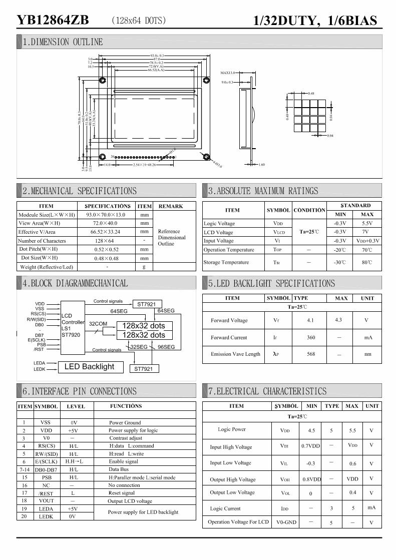
2. MECHANICAL SPECIFICATIONS
ITEM SPECIFICATIONS UNIT
Module Size 93.0L×70.0W×13.0(max)H mm
View Area 72.0×40.0 mm
Effective Area 128×64 dots
Dot Size 0.48×0.48 mm
Dot Pitch 0.52×0.52 mm
深 圳 市 亚 斌 电 子 有 限 公 司 SHENZHEN YABIN ELECTRONICS CO.,LTD
---------------------------------------------------------------------------------------------------------------------------------------------------------
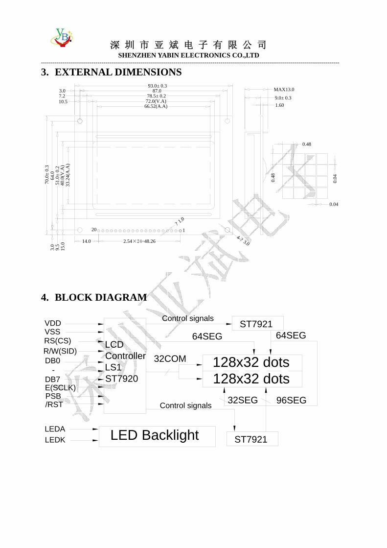
3. EXTERNAL DIMENSIONS
20
9.0± 0.31.60
MAX13.0
70.0
±0.
3
66.52(A.A)72.0(V.A)
87.093.0± 0.3
78.5± 0.2
64.0
0.04
0.04
0.48
0.48
1
33.2
4(A
.A)
40.0
(V.A
)51
.0±
0.2
2.54×24=48.2614.0
? 1.0
4-? 3.0
3.07.210.5
3.0
9.5
15.0
4. BLOCK DIAGRAM
VDDVSS
R/W(SID)RS(CS)
128x32 dots
LED BacklightLEDALEDK
LCDControllerLS1ST7920
ST7921
96SEG
32COM
64SEG
DB0 -DB7E(SCLK)PSB/RST
ST7921
128x32 dots
32SEG
Control signals
Control signals
64SEG
深 圳 市 亚 斌 电 子 有 限 公 司 SHENZHEN YABIN ELECTRONICS CO.,LTD
---------------------------------------------------------------------------------------------------------------------------------------------------------
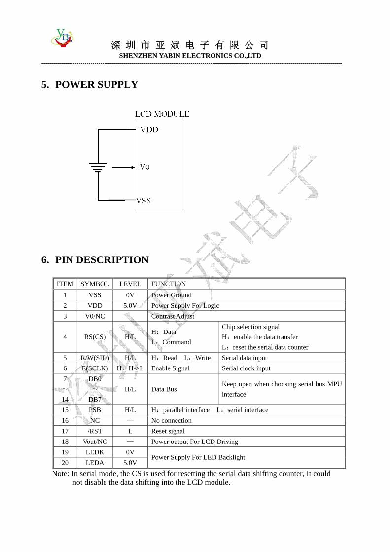
5. POWER SUPPLY
6. PIN DESCRIPTION
ITEM SYMBOL LEVEL FUNCTION 1 VSS 0V Power Ground 2 VDD 5.0V Power Supply For Logic 3 V0/NC — Contrast Adjust
4 RS(CS) H/L H:Data L:Command
Chip selection signal H:enable the data transfer L:reset the serial data counter
5 R/W(SID) H/L H:Read L:Write Serial data input 6 E(SCLK) H,H->L Enable Signal Serial clock input 7 ~ 14
DB0 ~
DB7 H/L Data Bus
Keep open when choosing serial bus MPU interface
15 PSB H/L H:parallel interface L:serial interface 16 NC — No connection 17 /RST L Reset signal 18 Vout/NC — Power output For LCD Driving 19 LEDK 0V 20 LEDA 5.0V
Power Supply For LED Backlight
Note: In serial mode, the CS is used for resetting the serial data shifting counter, It could not disable the data shifting into the LCD module.
深 圳 市 亚 斌 电 子 有 限 公 司 SHENZHEN YABIN ELECTRONICS CO.,LTD
---------------------------------------------------------------------------------------------------------------------------------------------------------
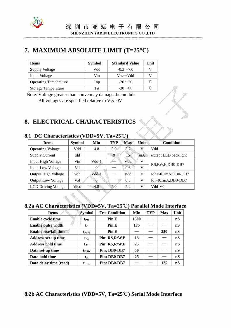
7. MAXIMUM ABSOLUTE LIMIT (T=25°C)
Items Symbol Standard Value UnitSupply Voltage Vdd -0.3~7.0 V Input Voltage Vin Vss~Vdd V Operating Temperature Top -20~70 ℃ Storage Temperature Tst -30~80 ℃
Note: Voltage greater than above may damage the module All voltages are specified relative to VSS=0V
8. ELECTRICAL CHARACTERISTICS 8.1 DC Characteristics (VDD=5V, Ta=25℃)
Items Symbol Min TYP Max Unit Condition Operating Voltage Vdd 4.8 5.0 5.2 V Vdd Supply Current Idd — 8 15 mA except LED backlight Input High Voltage Vin Vdd-1 — Vdd V Input Low Voltage Vil 0 — 0.6 V
RS,RW,E,DB0-DB7
Output High Voltage Voh Vdd-1 — Vdd V Ioh=-0.1mA,DB0-DB7 Output Low Voltage Vol 0 — 0.5 V Iol=0.1mA,DB0-DB7 LCD Driving Voltage Vlcd 4.8 5.0 5.2 V Vdd-V0
8.2 a AC Characteristics (VDD=5V, Ta=25℃) Parallel Mode Interface
Items Symbol Test Condition Min TYP Max Unit Enable cycle time tPW Pin E 1500 — — nS Enable pulse width tC Pin E 175 — — nS Enable rise/fall time tR,tF Pin E — — 250 nS Address set-up time tAS Pin: RS,R/W,E 13 — — nS Address hold time tAH Pin: RS,R/W,E 25 — — nS Data set-up time tDSW Pin: DB0-DB7 50 — — nS Data hold time tH Pin: DB0-DB7 25 — — nS Data delay time (read) tDDR Pin: DB0-DB7 — — 125 nS
8.2 b AC Characteristics (VDD=5V, Ta=25℃) Serial Mode Interface
深 圳 市 亚 斌 电 子 有 限 公 司 SHENZHEN YABIN ELECTRONICS CO.,LTD
---------------------------------------------------------------------------------------------------------------------------------------------------------
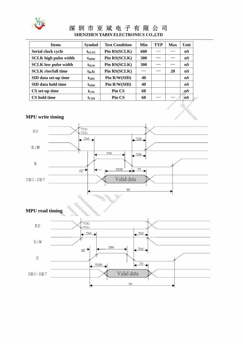
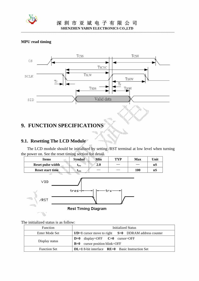
Items Symbol Test Condition Min TYP Max Unit Serial clock cycle tSCYC Pin RS(SCLK) 600 — — nS SCLK high pulse width tSHW Pin RS(SCLK) 300 — — nS SCLK low pulse width tSLW Pin RS(SCLK) 300 — — nS SCLK rise/fall time tR,tF Pin RS(SCLK) — — 20 nS SID data set-up time tSDS Pin R/W(SID) 40 nS SID data hold time tSDH Pin R/W(SID) 40 nS CS set-up time tCSS Pin CS 60 nS CS hold time tCSH Pin CS 60 — — nS
MPU write timing
MPU read timing
深 圳 市 亚 斌 电 子 有 限 公 司 SHENZHEN YABIN ELECTRONICS CO.,LTD
---------------------------------------------------------------------------------------------------------------------------------------------------------
MPU read timing
9. FUNCTION SPECIFICATIONS
9.1. Resetting The LCD Module The LCD module should be initialized by setting /RST terminal at low level when turning
the power on. See the reset timing section for detail. Items Symbol Min TYP Max Unit
Reset pulse width trw 2.0 — — uS Reset start time tres — — 100 nS
The initialized status is as follow:
Function Initialized Status Enter Mode Set I/D=1 cursor move to right S=0 DDRAM address counter
Display status D=0 display=OFF C=0 cursor=OFF B=0 cursor position blink=OFF
Function Set DL=1 8-bit interface RE=0 Basic Instruction Set
深 圳 市 亚 斌 电 子 有 限 公 司 SHENZHEN YABIN ELECTRONICS CO.,LTD
---------------------------------------------------------------------------------------------------------------------------------------------------------
Scroll Or RAM Address select SR=0 CGRAM address access is enable Reverse R1=1,R0=0 First line normal
Extended Function Set G=0 Graphic display OFF
9.2. Using Parallel Interface When PSB=H, the LCD module is in parallel interface mode. 8-bit or 4-bit bus interface could be selected by FUNCTION SET instruction DL bit. In 4-bit bus interface, every 8-bit instruction/data is separated into two parts. First, transfer the higher 4-bit(D7-D4), then transfer the lower 4-bit(D3-D0). They are transferred via DB7-DB4 terminals, where DB3-DB0 are not in used (leave open or pull high).
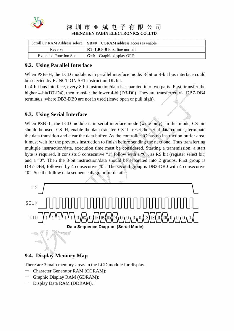
9.3. Using Serial Interface When PSB=L, the LCD module is in serial interface mode (write only). In this mode, CS pin should be used. CS=H, enable the data transfer. CS=L, reset the serial data counter, terminate the data transition and clear the data buffer. As the controller IC has no instruction buffer area, it must wait for the previous instruction to finish before sending the next one. Thus transferring multiple instruction/data, execution time must be considered. Starting a transmission, a start byte is required. It consists 5 consecutive “1” follow with a “0”, as RS bit (register select bit) and a “0”. Then the 8-bit instruction/data should be separated into 2 groups. First group is DB7-DB4, followed by 4 consecutive “0”. The second group is DB3-DB0 with 4 consecutive “0”. See the follow data sequence diagram for detail:
9.4. Display Memory Map There are 3 main memory-areas in the LCD module for display. 一 Character Generator RAM (CGRAM); 一 Graphic Display RAM (GDRAM); 一 Display Data RAM (DDRAM).
深 圳 市 亚 斌 电 子 有 限 公 司 SHENZHEN YABIN ELECTRONICS CO.,LTD
---------------------------------------------------------------------------------------------------------------------------------------------------------
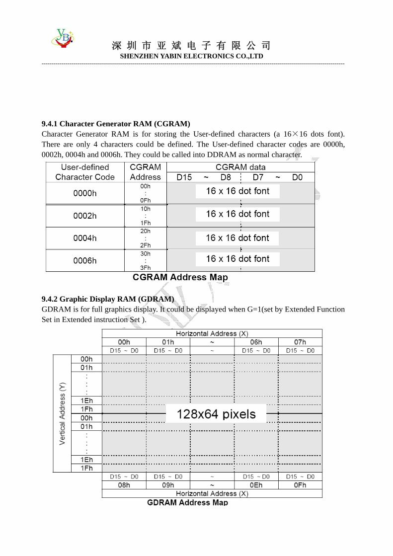
9.4.1 Character Generator RAM (CGRAM) Character Generator RAM is for storing the User-defined characters (a 16×16 dots font). There are only 4 characters could be defined. The User-defined character codes are 0000h, 0002h, 0004h and 0006h. They could be called into DDRAM as normal character.
9.4.2 Graphic Display RAM (GDRAM) GDRAM is for full graphics display. It could be displayed when G=1(set by Extended Function Set in Extended instruction Set ).
深 圳 市 亚 斌 电 子 有 限 公 司 SHENZHEN YABIN ELECTRONICS CO.,LTD
---------------------------------------------------------------------------------------------------------------------------------------------------------
Note: 一 The mapping is based on Vertical Scroll Displacement Address=0; 一 Another 128×64 Graphics display RAM space is not showed. They could be displayed
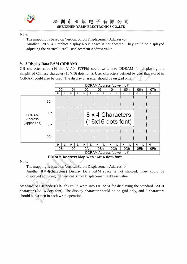
adjusting the Vertical Scroll Displacement Address value. 9.4.3 Display Data RAM (DDRAM) GB character code (16-bit, A1A0h-F7FFh) could write into DDRAM for displaying the simplified Chinese character (16×16 dots font). User characters defined by user that stored in CGRAM could also be used. The display character should be on grid only.
Note: 一 The mapping is based on Vertical Scroll Displacement Address=0; 一 Another 8×4(characters) Display Data RAM space is not showed. They could be
displayed adjusting the Vertical Scroll Displacement Address value. Standard ASCII code (00h-7fh) could write into DDRAM for displaying the standard ASCII character (8×16 dots font). The display character should be on grid only, and 2 characters should be written in each write operation.
深 圳 市 亚 斌 电 子 有 限 公 司 SHENZHEN YABIN ELECTRONICS CO.,LTD
---------------------------------------------------------------------------------------------------------------------------------------------------------
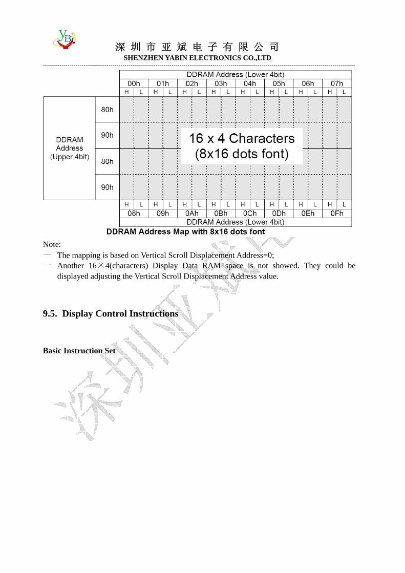
Note: 一 The mapping is based on Vertical Scroll Displacement Address=0; 一 Another 16×4(characters) Display Data RAM space is not showed. They could be
displayed adjusting the Vertical Scroll Displacement Address value.
9.5. Display Control Instructions
Basic Instruction Set
深 圳 市 亚 斌 电 子 有 限 公 司 SHENZHEN YABIN ELECTRONICS CO.,LTD
---------------------------------------------------------------------------------------------------------------------------------------------------------
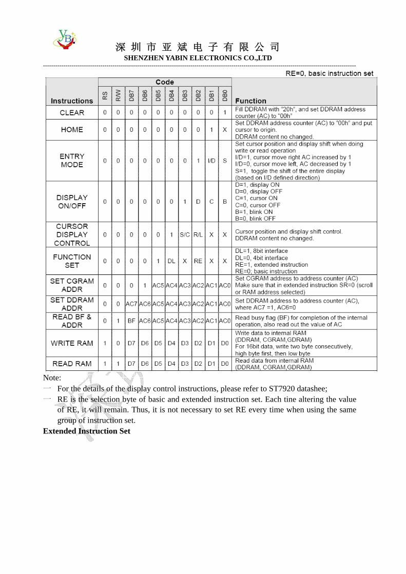
Note: 一 For the details of the display control instructions, please refer to ST7920 datashee; 一 RE is the selection byte of basic and extended instruction set. Each tine altering the value
of RE, it will remain. Thus, it is not necessary to set RE every time when using the same group of instruction set.
Extended Instruction Set
深 圳 市 亚 斌 电 子 有 限 公 司 SHENZHEN YABIN ELECTRONICS CO.,LTD
---------------------------------------------------------------------------------------------------------------------------------------------------------
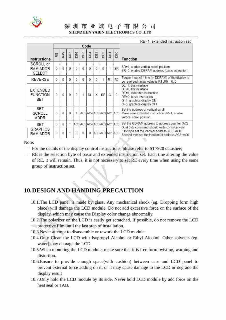
Note: 一 For the details of the display control instructions, please refer to ST7920 datashee; 一 RE is the selection byte of basic and extended instruction set. Each tine altering the value
of RE, it will remain. Thus, it is not necessary to set RE every time when using the same group of instruction set.
10. DESIGN AND HANDING PRECAUTION
10.1. The LCD panel is made by glass. Any mechanical shock (eg. Dropping form high place) will damage the LCD module. Do not add excessive force on the surface of the display, which may cause the Display color change abnormally.
10.2. The polarizer on the LCD is easily get scratched. If possible, do not remove the LCD protective film until the last step of installation.
10.3. Never attempt to disassemble or rework the LCD module. 10.4. Only Clean the LCD with Isopropyl Alcohol or Ethyl Alcohol. Other solvents (eg.
water) may damage the LCD. 10.5. When mounting the LCD module, make sure that it is free form twisting, warping and
distortion. 10.6. Ensure to provide enough space(with cushion) between case and LCD panel to
prevent external force adding on it, or it may cause damage to the LCD or degrade the display result
10.7. Only hold the LCD module by its side. Never hold LCD module by add force on the heat seal or TAB.


![[5936 - 12864]gestao_publica](https://img.pdfslide.tips/doc/110x75/553c1b95550346e0478b4732/5936-12864gestaopublica.jpg)