Embed Size (px)
Citation preview
State Key Lab of ASIC & Systems, Fudan University
Double Patterning
Wai-Shing Luk
State Key Lab of ASIC & Systems, Fudan University
Background
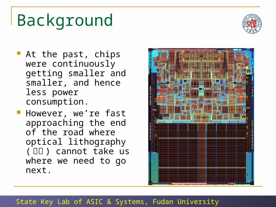
At the past, chips were continuously getting smaller and smaller, and hence less power consumption.
However, we’re fast approaching the end of the road where optical lithography(光刻 ) cannot take us where we need to go next.
State Key Lab of ASIC & Systems, Fudan University
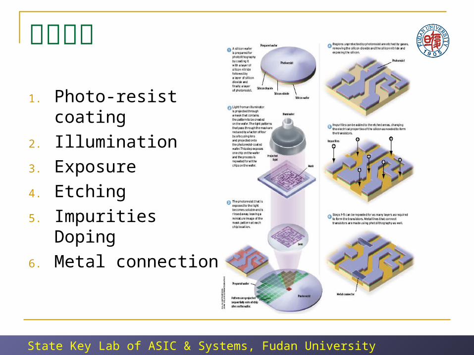
光刻过程
1. Photo-resist coating
2. Illumination
3. Exposure
4. Etching
5. Impurities Doping
6. Metal connection
State Key Lab of ASIC & Systems, Fudan University
Sub-wavelength Lithograph
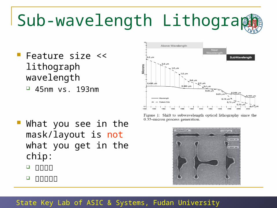
Feature size << lithograph wavelength 45nm vs. 193nm
What you see in the mask/layout is not what you get in the chip: 图形失真 成品率下降
State Key Lab of ASIC & Systems, Fudan University
What is Double Patterning?
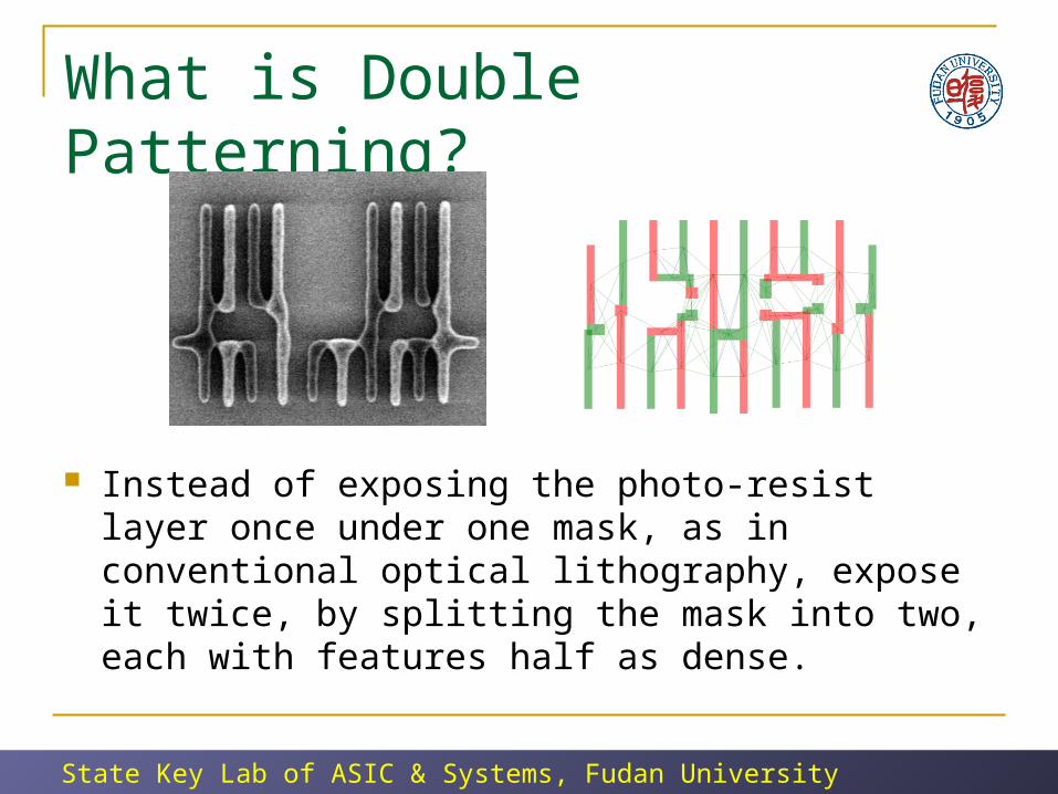
Instead of exposing the photo-resist layer once under one mask, as in conventional optical lithography, expose it twice, by splitting the mask into two, each with features half as dense.
State Key Lab of ASIC & Systems, Fudan University
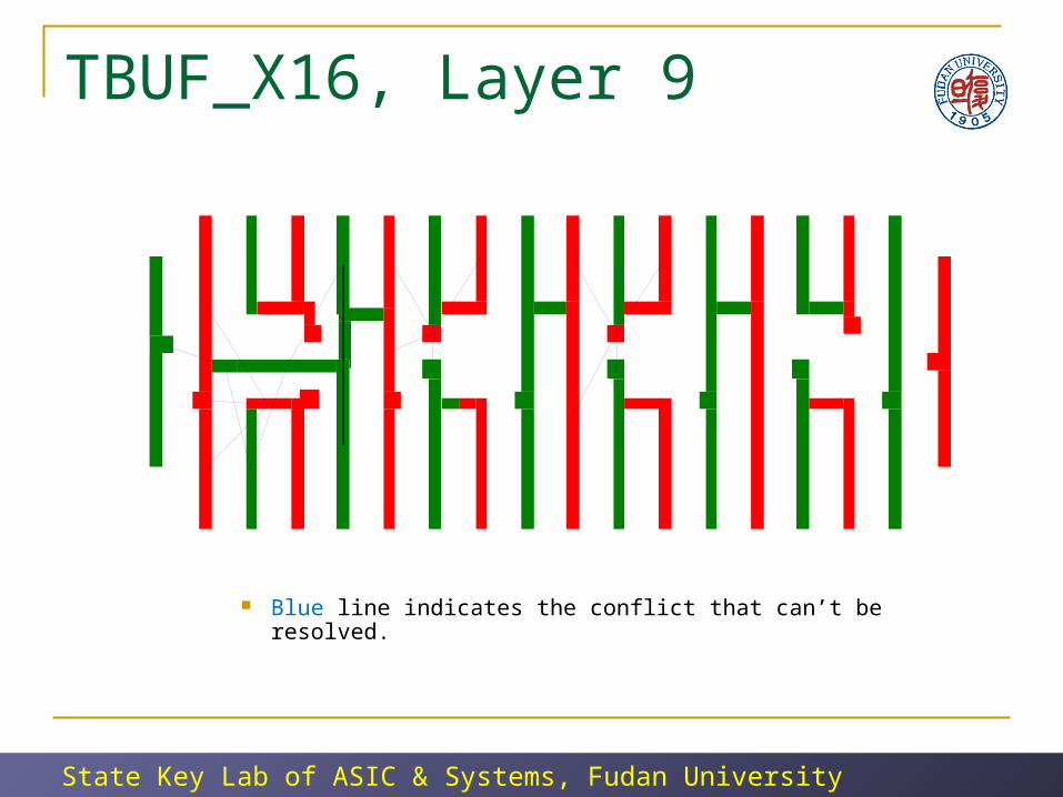
TBUF_X16, Layer 9
Blue line indicates the conflict that can’t be resolved.
State Key Lab of ASIC & Systems, Fudan University
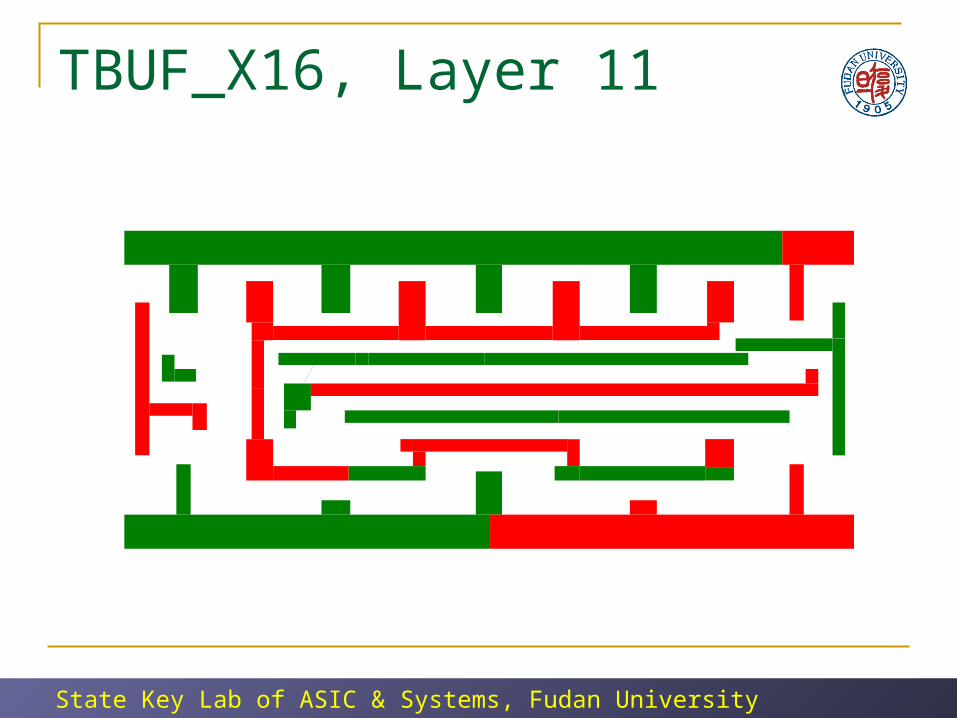
TBUF_X16, Layer 11
State Key Lab of ASIC & Systems, Fudan University
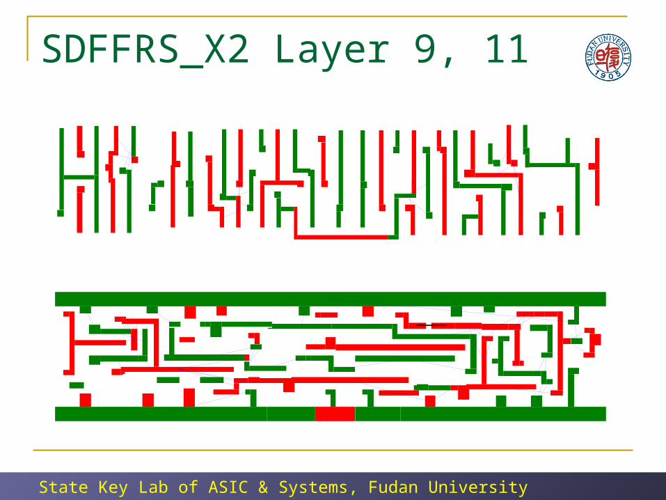
SDFFRS_X2 Layer 9, 11
State Key Lab of ASIC & Systems, Fudan University
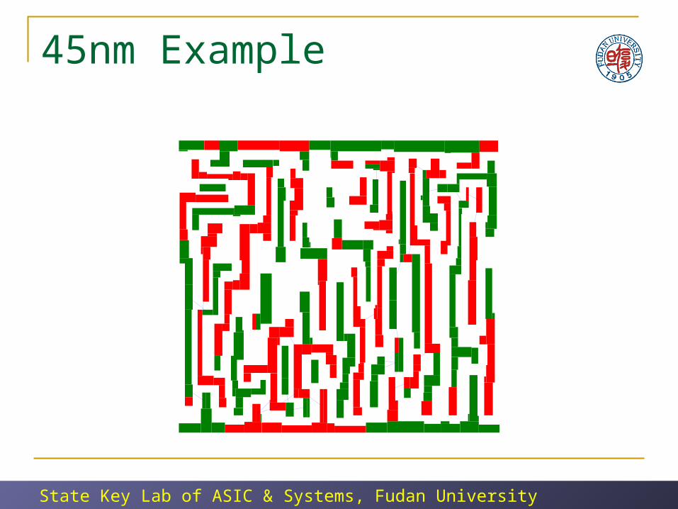
45nm Example
State Key Lab of ASIC & Systems, Fudan University
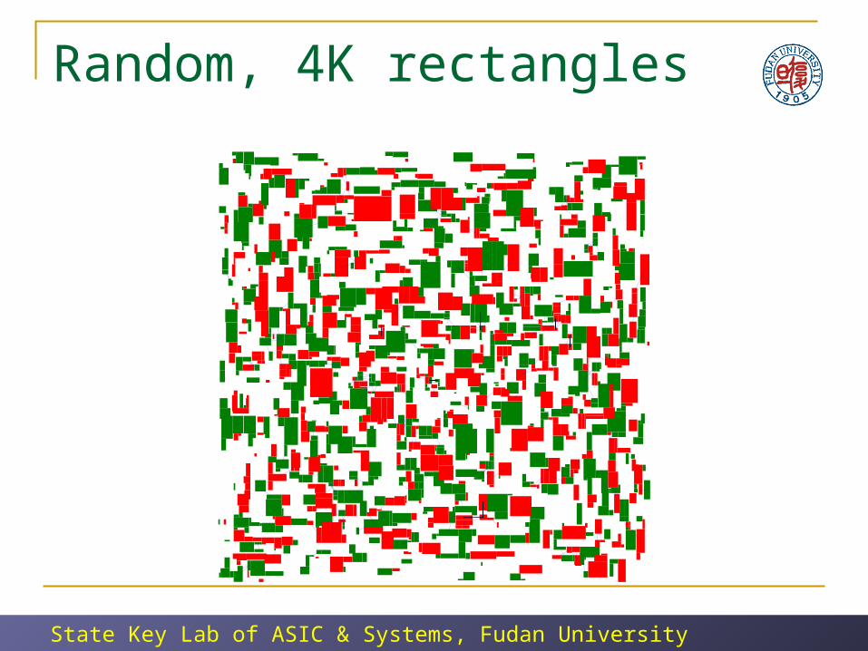
Random, 4K rectangles
State Key Lab of ASIC & Systems, Fudan University
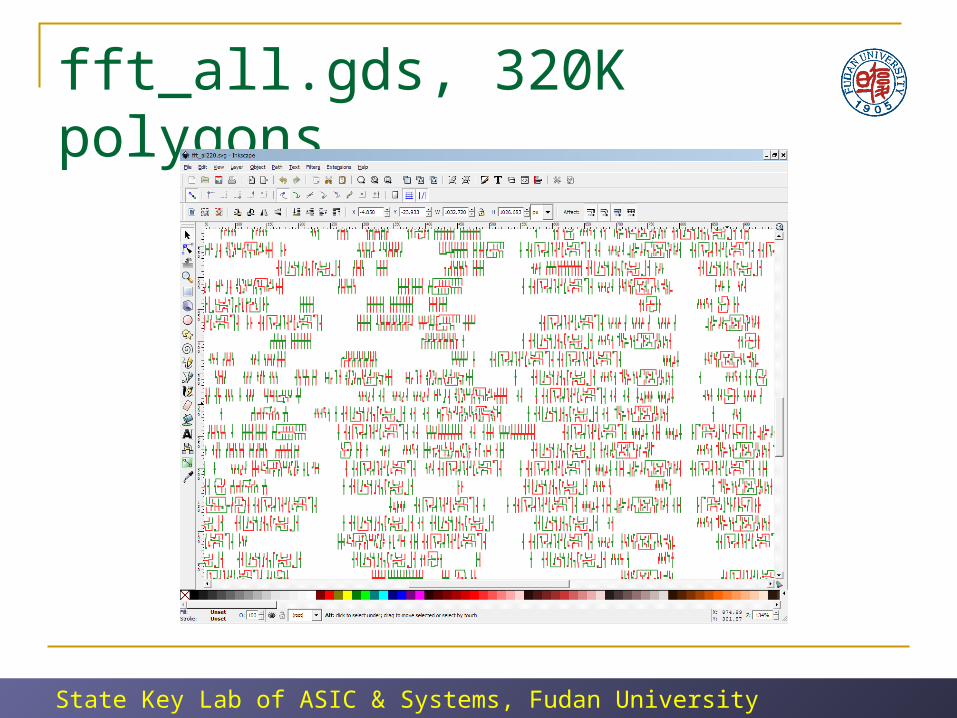
fft_all.gds, 320K polygons
State Key Lab of ASIC & Systems, Fudan University
Current Status of Our SW
fft_all: 320K polygons, 1.3M rectangles Conflict graph construction within 1 minute Color assignment within 9 minutes Compare: 26 minutes for just displaying the result
using “eog” Note: Only g++ 3.4.5 was used, no advanced
compiler optimization has been done yet.
State Key Lab of ASIC & Systems, Fudan University
Key Techniques
Novel polygon cutting algorithm to reduce the number of rectangles and the total cut-length.
Novel dynamic priority search tree for plane-sweeping.
Decompose the underlying conflict graph into its tri-connected components using SPQR-tree
Graph-theoretical approach instead of ILP Recast the coloring problem as a T-join problem and
is then by solved by Hadlock’s algorithm
State Key Lab of ASIC & Systems, Fudan University
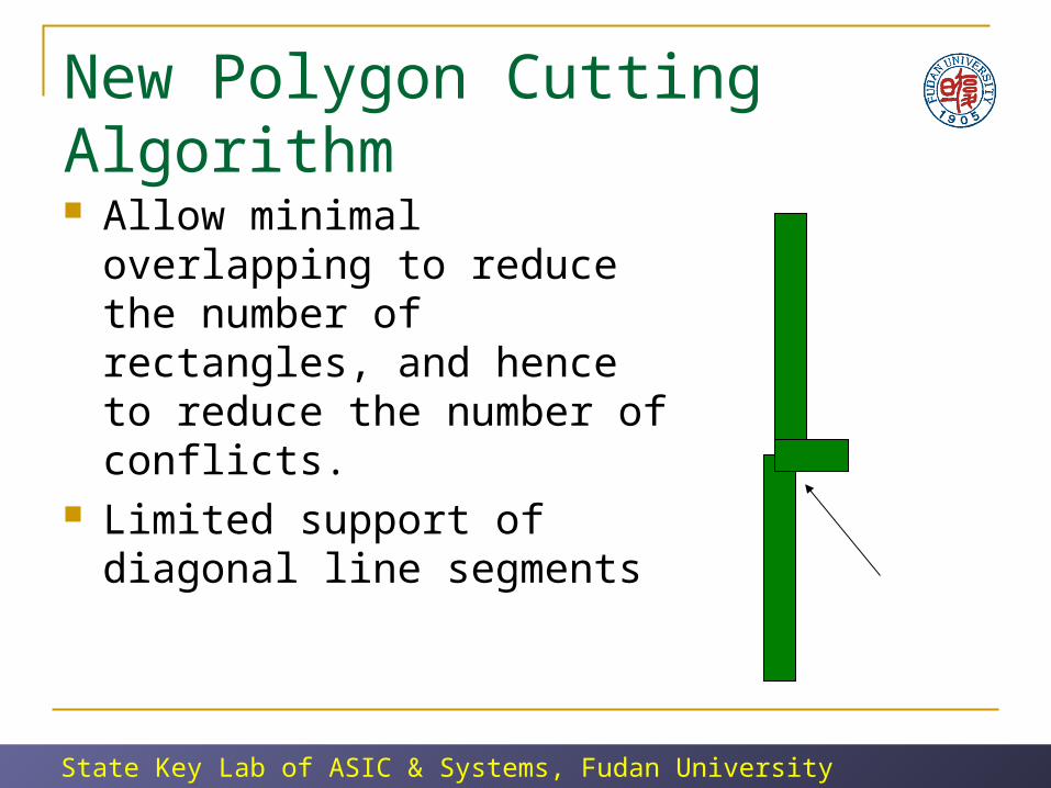
New Polygon Cutting Algorithm Allow minimal overlapping to
reduce the number of rectangles, and hence to reduce the number of conflicts.
Limited support of diagonal line segments
State Key Lab of ASIC & Systems, Fudan University
Dynamic Priority Search Tree In plane sweeping, events are frequently
“inserted” and “deleted” to the scan line. In our PST, all data are stored at the leaf
nodes of PST, making “insert” and “delete” operations very fast (O(1) time for each tree rotation). The payoff is that the “query” operation will be little slower than the traditional PST.
State Key Lab of ASIC & Systems, Fudan University
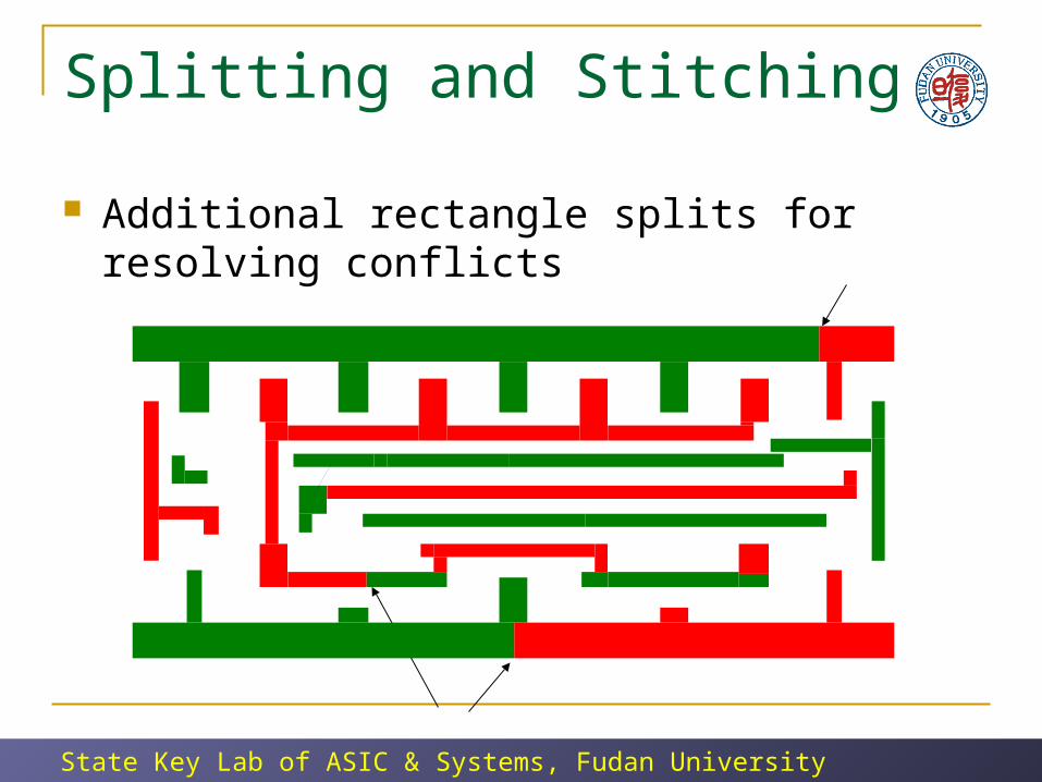
Splitting and Stitching
Additional rectangle splits for resolving conflicts
State Key Lab of ASIC & Systems, Fudan University
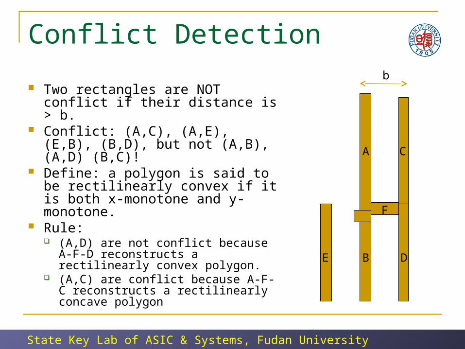
Conflict Detection
Two rectangles are NOT conflict if their distance is > b.
Conflict: (A,C), (A,E), (E,B), (B,D), but not (A,B), (A,D) (B,C)!
Define: a polygon is said to be rectilinearly convex if it is both x-monotone and y-monotone.
Rule: (A,D) are not conflict because A-F-D
reconstructs a rectilinearly convex polygon.
(A,C) are conflict because A-F-C reconstructs a rectilinearly concave polygon
A
B
C
DE
F
b
State Key Lab of ASIC & Systems, Fudan University
Layout Splitting Problem Formulation INSTANCE: Graph G = (V,E) and a weight function w : E N
SOLUTION: Disjoint vertex subsets V0 and V1 where V = V0 ∪ V1
MINIMIZE: the total cost of edges whose end vertices in same color.
Note: the problem is linear-time solvable for bipartite graphs, polynomial-time solvable for planar graphs, but NP-hard in general.
To reduce the problem size, graph partitioning techniques could be used.
State Key Lab of ASIC & Systems, Fudan University
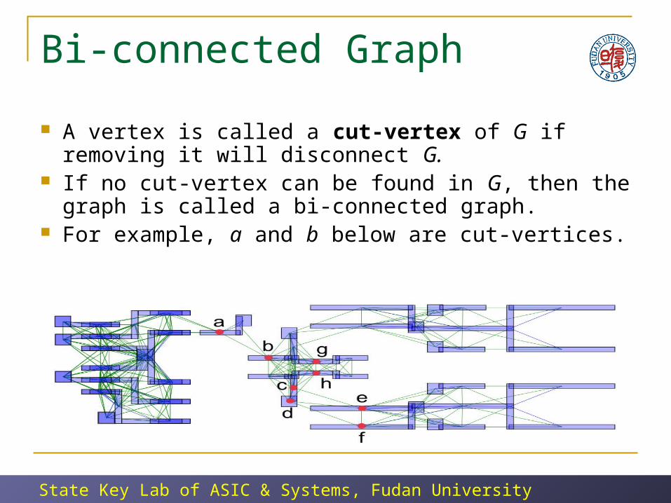
Bi-connected Graph
A vertex is called a cut-vertex of G if removing it will disconnect G.
If no cut-vertex can be found in G, then the graph is called a bi-connected graph.
For example, a and b below are cut-vertices.
State Key Lab of ASIC & Systems, Fudan University
Bi-connected Components
A connected graph can be decomposed into its bi-connected components in linear-time.
Each bi-connected component can be solved independently without affecting the final sol’n.
Question: Is it possible to further decompose the graph?
State Key Lab of ASIC & Systems, Fudan University
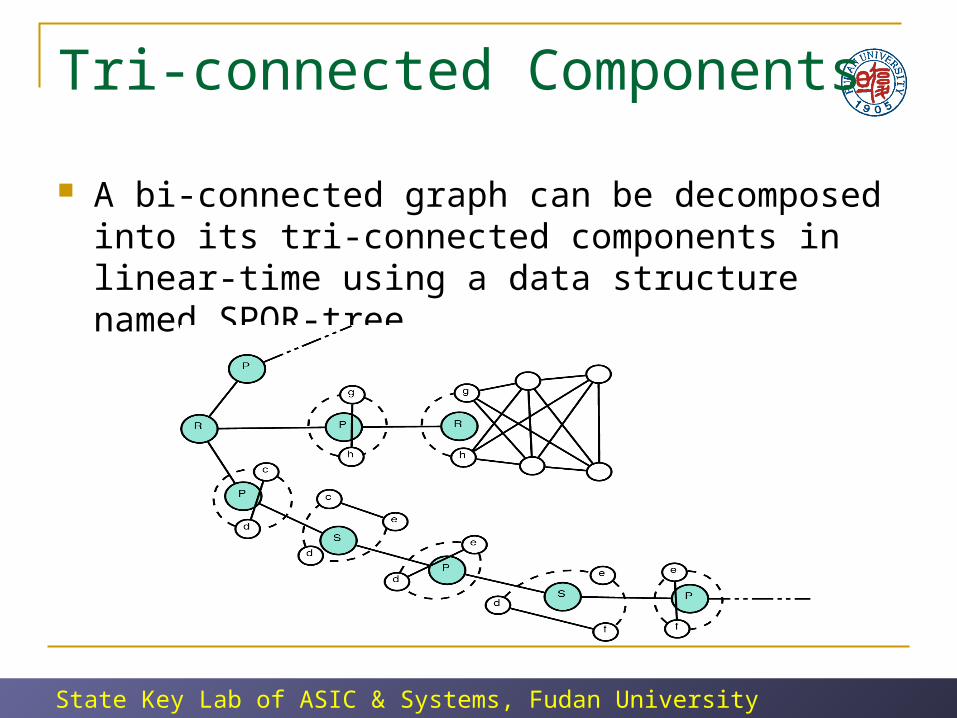
Tri-connected Graph
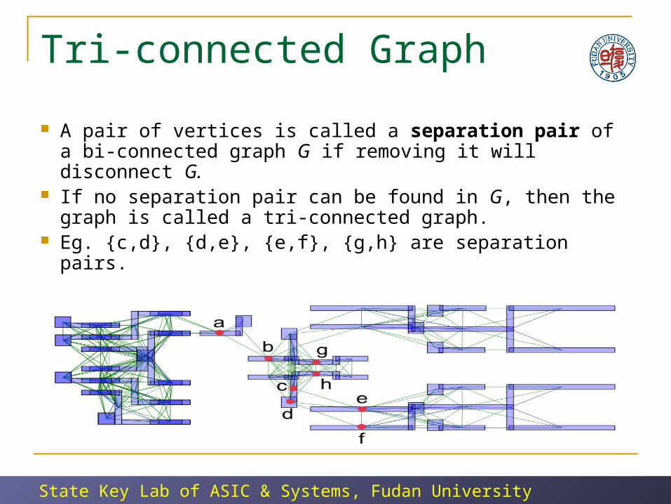
A pair of vertices is called a separation pair of a bi-connected graph G if removing it will disconnect G.
If no separation pair can be found in G, then the graph is called a tri-connected graph.
Eg. {c,d}, {d,e}, {e,f}, {g,h} are separation pairs.
State Key Lab of ASIC & Systems, Fudan University
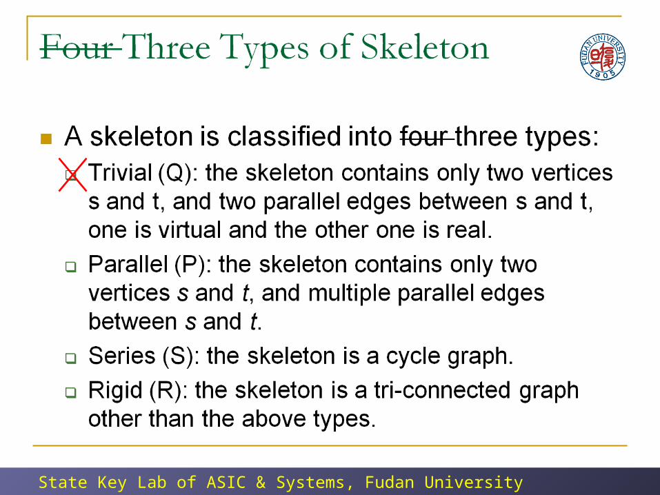
Tri-connected Components
A bi-connected graph can be decomposed into its tri-connected components in linear-time using a data structure named SPQR-tree
State Key Lab of ASIC & Systems, Fudan University
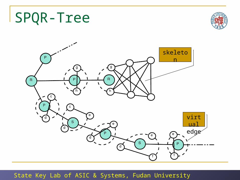
SPQR-Tree
virtual edge
skeleton
State Key Lab of ASIC & Systems, Fudan University
State Key Lab of ASIC & Systems, Fudan University
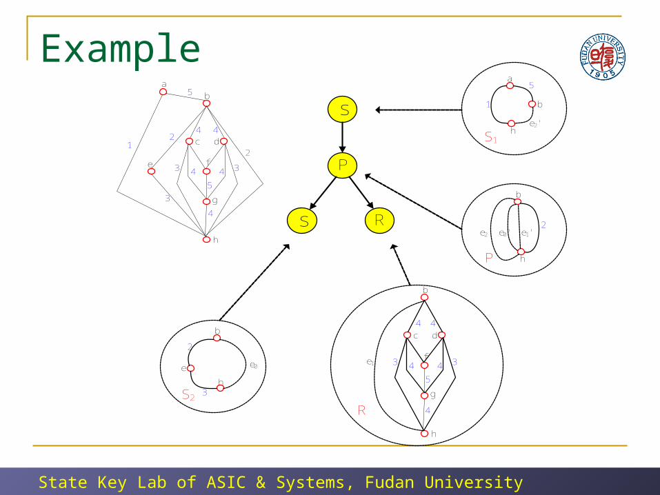
Divide-and-Conquer Method
Three basic steps: Divide a graph into its tri-connected components. Solve each tri-connected components in a
bottom-up fashion. Merge the solutions into a complete one in a top-
down fashion.
We calculate two possible solutions for each components, namely {s, t} in same color and {s, t} in opposite colors.
State Key Lab of ASIC & Systems, Fudan University
Examples
P
s R
b
h
e e0
S2
2
3
S1
a
b
h
1
5
a
b
c d
e f
g
h
12
3
3 4 4 3
2
5
5
4
4 4
b
hP
2e0' e1'
b
c d
f
g
h
3 4 4 3
5
44
R 4
e1
e2
e2'
State Key Lab of ASIC & Systems, Fudan University
More Technical Details
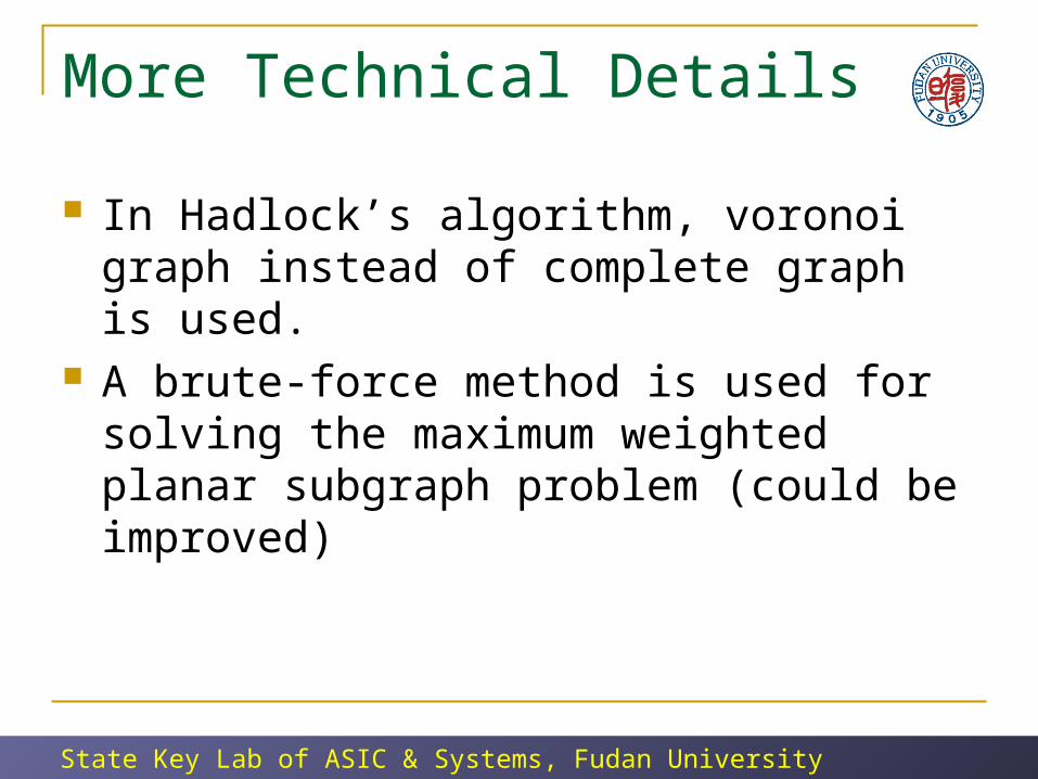
In Hadlock’s algorithm, voronoi graph instead of complete graph is used.
A brute-force method is used for solving the maximum weighted planar subgraph problem (could be improved)
State Key Lab of ASIC & Systems, Fudan University
Conclusions
Experiment results show that our method can achieve 3-10X speedup
We believe that it is a key to the success of 22nm process
Unfortunately we didn’t have chance to try a realistic 32/22nm layout yet
because nearly everything is confidential under 90nm
Foundries may move to EUV if DPL fails.