Embed Size (px)
Citation preview

LT-61515E SERVICE MANUAL CONTENT PART 1:Brief Introduction Of The LT-61515E
Schematic Diagram Printed Circuit
PART 2: Exploded view PART 3:Key Ics And Assemblies PART 4: Detailed Circuit Main Board DVD Board
HI-voltage Board
PART 5: Parts List PART6: Debug Procedure
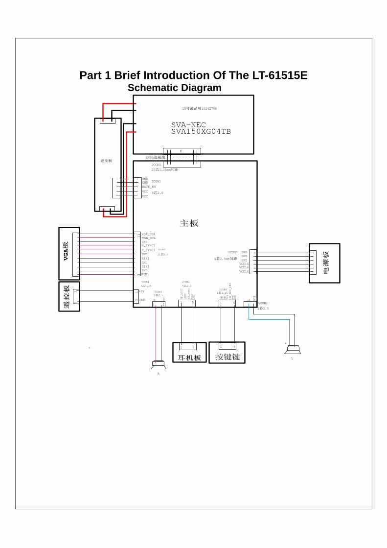
Part 1 Brief Introduction Of The LT-61515E Schematic Diagram
GND
1CON7
61
B
H_SYNC1GND
GND
VCC
1
2芯2.5
GNDGND
GND
5CON1
5芯2.0
VCC16
遥控
板
BIN1
++
耳机板
L
VCC16
2芯2.5
5芯1.25
GND
20芯1.25mm间距
1
6芯1.25
1CON4
GIN1
1CON2
2CON1GN
D
1CON8
GND
GND
VCCGND
VCC16
L
5芯2.0
RIN1
ROUT
SVA-NECSVA150XG04TB
15寸液晶屏1024X768
KEY
_ADC_
IN3
1
GND
+5V
11
SP_R
OUT
3CON1
LVDS连接线
IN3
GND
51
11芯2.0
LOUT
GND
5CON2
逆变板
IN2
按键键
1
1CON1
SP_L
OUT
BACK_EN
IN1
VGA_SDA
主板
6
VG
A板
5
V_SYNC1
GND
1
R
5
VGA_SCL
R
6芯2.5mm间距
2
电源
板
5 1

Printed Circuit Main Board 3912C (Top View)

Main Board 3912C (Bottom view)
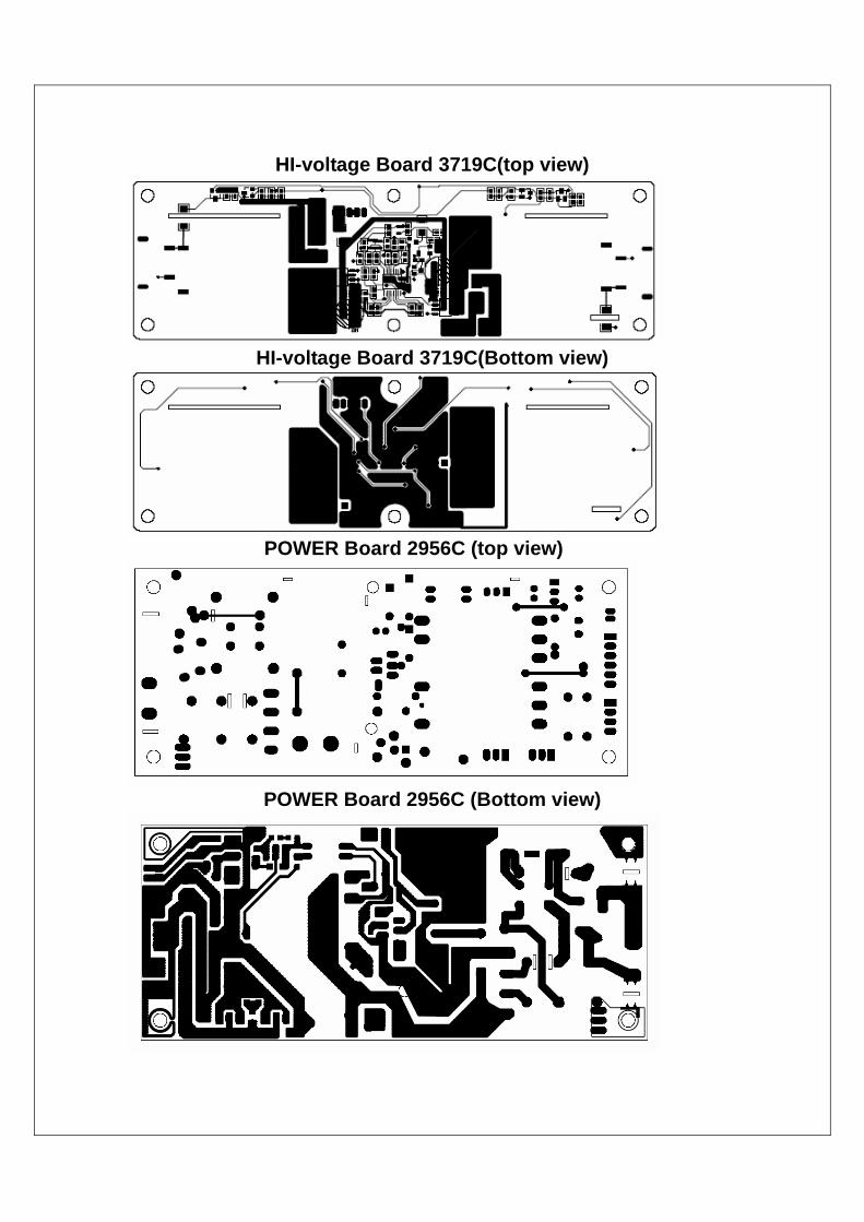
HI-voltage Board 3719C(top view)
HI-voltage Board 3719C(Bottom view)
POWER Board 2956C (top view)
POWER Board 2956C (Bottom view)
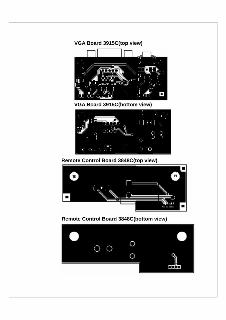
VGA Board 3915C(top view)
VGA Board 3915C(bottom view)
Remote Control Board 3848C(top view)
Remote Control Board 3848C(bottom view)

Earphone board3951C (top view)
Earphone board3951C (bottom view)
Key board3950C (top view)
Key board3950C (bottom view)

PART 2 Exploded view
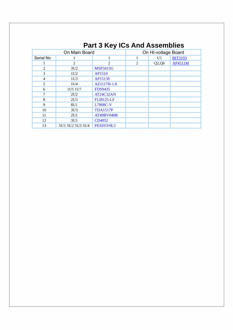
Part 3 Key ICs And Assemblies On Main Board On HI-voltage Board
Serial No 1 1 1 U1 BIT3193 1 2 2 2 Q2,Q6 AP4511M 2 3U2 MSP3415G 3 1U2 AP1510 4 1U3 AP1513S 5 1U4 AZ1117H-1.8 6 1U5 1U7 FDS9435 7 2U2 AT24C32AN 8 2U3 FLI8125-LF 9 8U1 L7808C-V
10 3U3 TDA1517P 11 2U1 AT49BV040B 12 3U1 CD4052 13 5U1 5U2 5U3 5U4 PESD5V0L5

ICS ON MAIN BOARD 1. AP1513
·Block Diagram
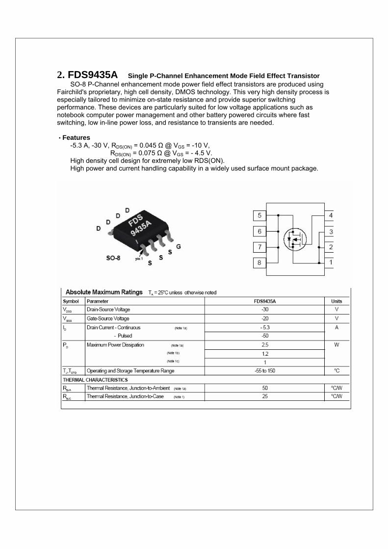
2. FDS9435A Single P-Channel Enhancement Mode Field Effect Transistor SO-8 P-Channel enhancement mode power field effect transistors are produced using
Fairchild's proprietary, high cell density, DMOS technology. This very high density process is especially tailored to minimize on-state resistance and provide superior switching performance. These devices are particularly suited for low voltage applications such as notebook computer power management and other battery powered circuits where fast switching, low in-line power loss, and resistance to transients are needed. ·Features
-5.3 A, -30 V, RDS(ON) = 0.045 Ω @ VGS = -10 V, RDS(ON) = 0.075 Ω @ VGS = - 4.5 V.
High density cell design for extremely low RDS(ON). High power and current handling capability in a widely used surface mount package.
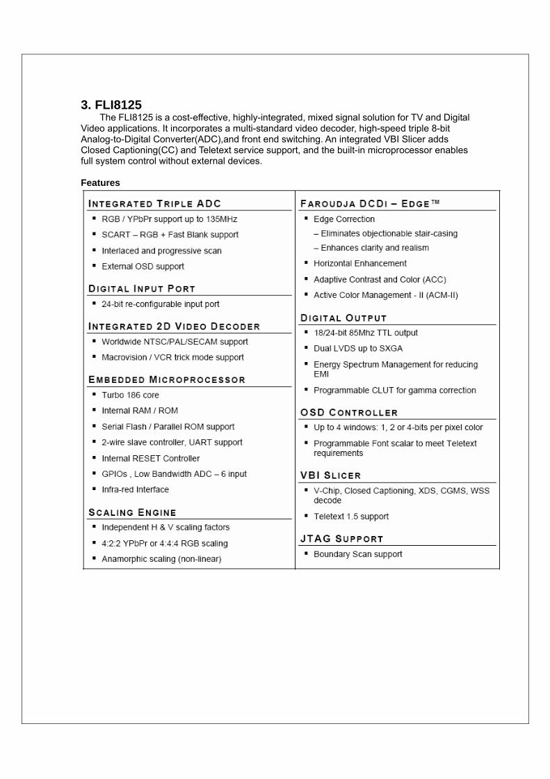
3. FLI8125 The FLI8125 is a cost-effective, highly-integrated, mixed signal solution for TV and Digital
Video applications. It incorporates a multi-standard video decoder, high-speed triple 8-bit Analog-to-Digital Converter(ADC),and front end switching. An integrated VBI Slicer adds Closed Captioning(CC) and Teletext service support, and the built-in microprocessor enables full system control without external devices.
Features
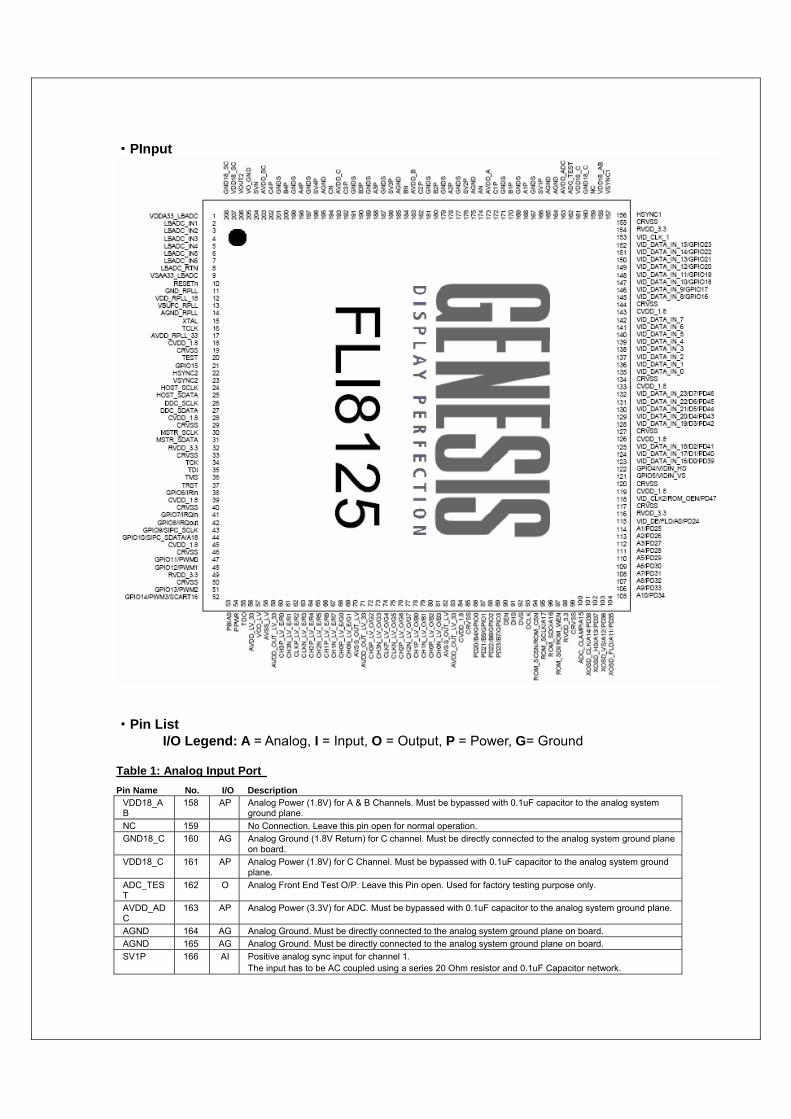
·PInput
·Pin List
I/O Legend: A = Analog, I = Input, O = Output, P = Power, G= Ground
Table 1: Analog Input Port Pin Name No. I/O Description
VDD18_AB
158 AP Analog Power (1.8V) for A & B Channels. Must be bypassed with 0.1uF capacitor to the analog system ground plane.
NC 159 No Connection. Leave this pin open for normal operation. GND18_C 160 AG Analog Ground (1.8V Return) for C channel. Must be directly connected to the analog system ground plane
on board. VDD18_C 161 AP Analog Power (1.8V) for C Channel. Must be bypassed with 0.1uF capacitor to the analog system ground
plane. ADC_TEST
162 O Analog Front End Test O/P. Leave this Pin open. Used for factory testing purpose only.
AVDD_ADC
163 AP Analog Power (3.3V) for ADC. Must be bypassed with 0.1uF capacitor to the analog system ground plane.
AGND 164 AG Analog Ground. Must be directly connected to the analog system ground plane on board. AGND 165 AG Analog Ground. Must be directly connected to the analog system ground plane on board. SV1P 166 AI Positive analog sync input for channel 1.
The input has to be AC coupled using a series 20 Ohm resistor and 0.1uF Capacitor network.
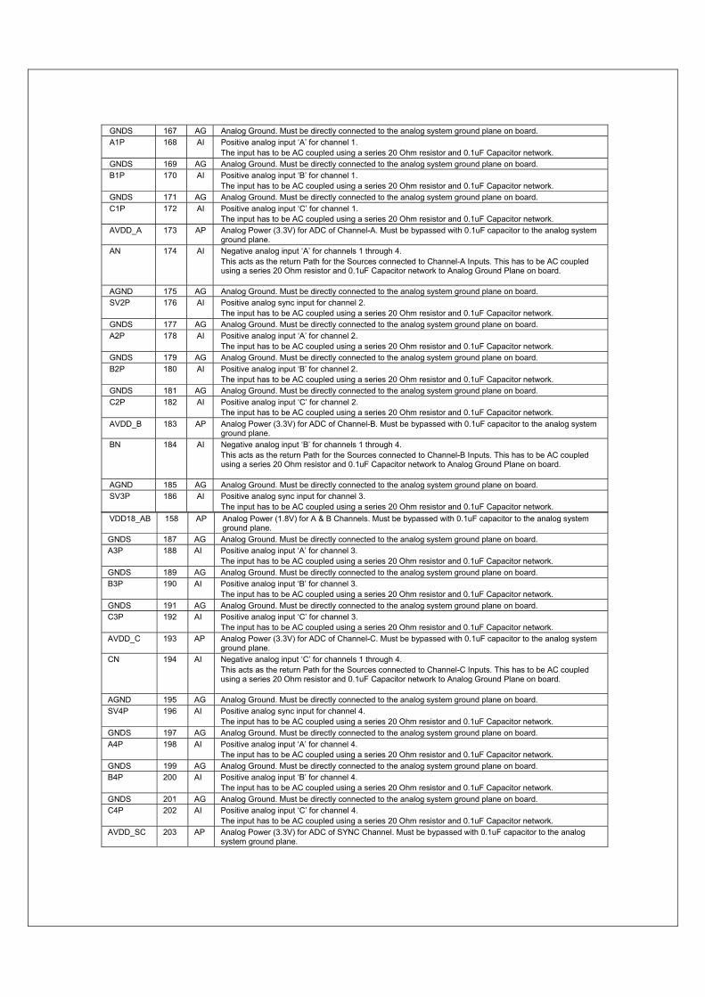
GNDS 167 AG Analog Ground. Must be directly connected to the analog system ground plane on board. A1P 168 AI Positive analog input ‘A’ for channel 1.
The input has to be AC coupled using a series 20 Ohm resistor and 0.1uF Capacitor network. GNDS 169 AG Analog Ground. Must be directly connected to the analog system ground plane on board. B1P 170 AI Positive analog input ‘B’ for channel 1.
The input has to be AC coupled using a series 20 Ohm resistor and 0.1uF Capacitor network. GNDS 171 AG Analog Ground. Must be directly connected to the analog system ground plane on board. C1P 172 AI Positive analog input ‘C’ for channel 1.
The input has to be AC coupled using a series 20 Ohm resistor and 0.1uF Capacitor network. AVDD_A 173 AP Analog Power (3.3V) for ADC of Channel-A. Must be bypassed with 0.1uF capacitor to the analog system
ground plane. AN 174 AI Negative analog input ‘A’ for channels 1 through 4.
This acts as the return Path for the Sources connected to Channel-A Inputs. This has to be AC coupled using a series 20 Ohm resistor and 0.1uF Capacitor network to Analog Ground Plane on board.
AGND 175 AG Analog Ground. Must be directly connected to the analog system ground plane on board. SV2P 176 AI Positive analog sync input for channel 2.
The input has to be AC coupled using a series 20 Ohm resistor and 0.1uF Capacitor network. GNDS 177 AG Analog Ground. Must be directly connected to the analog system ground plane on board. A2P 178 AI Positive analog input ‘A’ for channel 2.
The input has to be AC coupled using a series 20 Ohm resistor and 0.1uF Capacitor network. GNDS 179 AG Analog Ground. Must be directly connected to the analog system ground plane on board. B2P 180 AI Positive analog input ‘B’ for channel 2.
The input has to be AC coupled using a series 20 Ohm resistor and 0.1uF Capacitor network. GNDS 181 AG Analog Ground. Must be directly connected to the analog system ground plane on board. C2P 182 AI Positive analog input ‘C’ for channel 2.
The input has to be AC coupled using a series 20 Ohm resistor and 0.1uF Capacitor network. AVDD_B 183 AP Analog Power (3.3V) for ADC of Channel-B. Must be bypassed with 0.1uF capacitor to the analog system
ground plane. BN 184 AI Negative analog input ‘B’ for channels 1 through 4.
This acts as the return Path for the Sources connected to Channel-B Inputs. This has to be AC coupled using a series 20 Ohm resistor and 0.1uF Capacitor network to Analog Ground Plane on board.
AGND 185 AG Analog Ground. Must be directly connected to the analog system ground plane on board. SV3P 186 AI Positive analog sync input for channel 3.
The input has to be AC coupled using a series 20 Ohm resistor and 0.1uF Capacitor network. VDD18_AB 158 AP Analog Power (1.8V) for A & B Channels. Must be bypassed with 0.1uF capacitor to the analog system
ground plane. GNDS 187 AG Analog Ground. Must be directly connected to the analog system ground plane on board. A3P 188 AI Positive analog input ‘A’ for channel 3.
The input has to be AC coupled using a series 20 Ohm resistor and 0.1uF Capacitor network. GNDS 189 AG Analog Ground. Must be directly connected to the analog system ground plane on board. B3P 190 AI Positive analog input ‘B’ for channel 3.
The input has to be AC coupled using a series 20 Ohm resistor and 0.1uF Capacitor network. GNDS 191 AG Analog Ground. Must be directly connected to the analog system ground plane on board. C3P 192 AI Positive analog input ‘C’ for channel 3.
The input has to be AC coupled using a series 20 Ohm resistor and 0.1uF Capacitor network. AVDD_C 193 AP Analog Power (3.3V) for ADC of Channel-C. Must be bypassed with 0.1uF capacitor to the analog system
ground plane. CN 194 AI Negative analog input ‘C’ for channels 1 through 4.
This acts as the return Path for the Sources connected to Channel-C Inputs. This has to be AC coupled using a series 20 Ohm resistor and 0.1uF Capacitor network to Analog Ground Plane on board.
AGND 195 AG Analog Ground. Must be directly connected to the analog system ground plane on board. SV4P 196 AI Positive analog sync input for channel 4.
The input has to be AC coupled using a series 20 Ohm resistor and 0.1uF Capacitor network. GNDS 197 AG Analog Ground. Must be directly connected to the analog system ground plane on board. A4P 198 AI Positive analog input ‘A’ for channel 4.
The input has to be AC coupled using a series 20 Ohm resistor and 0.1uF Capacitor network. GNDS 199 AG Analog Ground. Must be directly connected to the analog system ground plane on board. B4P 200 AI Positive analog input ‘B’ for channel 4.
The input has to be AC coupled using a series 20 Ohm resistor and 0.1uF Capacitor network. GNDS 201 AG Analog Ground. Must be directly connected to the analog system ground plane on board. C4P 202 AI Positive analog input ‘C’ for channel 4.
The input has to be AC coupled using a series 20 Ohm resistor and 0.1uF Capacitor network. AVDD_SC 203 AP Analog Power (3.3V) for ADC of SYNC Channel. Must be bypassed with 0.1uF capacitor to the analog
system ground plane.

SVN 204 AI Negative analog sync input for channels 1 through 4. This acts as the return Path for the Sources connected to SV Channel Inputs. This has to be AC coupled using a series 20 Ohm resistor and 0.1uF Capacitor network to Analog Ground Plane on board.
VO_GND 205 AG Analog Ground. Must be directly connected to the analog system ground plane on board. VOUT2 206 AO Analog VOUT signal
This is the Analog Video Output from the Decoder in the Composite Video format. This can be amplified and be fed to any video display device.
VDD18_SC 207 AP Analog Power (1.8V) for SYNC Channel. Must be bypassed with 0.1uF capacitor to the analog system ground plane.
GND18_SC 208 AG Analog Ground (1.8V Return) for SYNC channel. Must be directly connected to the analog system ground plane on board.
Table 2: Low Bandwidth ADC Input Port Pin Name No I/O Description VDDA33_LBADC 1 AP Analog Power (3.3V) for Low Bandwidth ADC Block. Must be bypassed with 0.1uF capacitor. LBADC_IN1 2 AI Low Bandwidth Analog Input-1. The Input signal connected to this Pin, must be bypassed with a 0.1uF
capacitor and could be in the range of 0V to 3.3V (peak to peak). LBADC_IN2 3 AI Low Bandwidth Analog Input-2. The Input signal connected to this Pin, must be bypassed with a 0.1uF
capacitor and could be in the range of 0V to 3.3V (peak to peak). LBADC_IN3 4 AI Low Bandwidth Analog Input-3. The Input signal connected to this Pin, must be bypassed with a 0.1uF
capacitor and could be in the range of 0V to 3.3V (peak to peak). LBADC_IN4 5 AI Low Bandwidth Analog Input-4. The Input signal connected to this Pin, must be bypassed with a 0.1uF
capacitor and could be in the range of 0V to 3.3V (peak to peak). LBADC_IN5 6 AI Low Bandwidth Analog Input-5. The Input signal connected to this Pin, must be bypassed with a 0.1uF
capacitor and could be in the range of 0V to 3.3V (peak to peak). LBADC_IN6 7 AI Low Bandwidth Analog Input-6. The Input signal connected to this Pin, must be bypassed with LBADC_RTN 8 AG This Pin provides the Return Path for LBADC inputs. Must be directly connected to the analog system
ground plane on board. VSSA33_LBADC 9 AG Analog Ground for Low Bandwidth ADC Block. Must be directly connected to the analog system ground
plane on board.
Table 3: RCLK PLL Pins Pin Name No I/O Description GND_RPLL 11 DG Digital GND for ADC clocking circuit. Must be directly connected to the digital system ground plane.
VDD_RPLL_18 12 DP Digital power (1.8V) for ADC digital logic. Must be bypassed with capacitor to Ground Plane. VBUFC_RPLL 13 O Test Output. Leave this Pin Open. This is reserved for Factory Testing Purpose. AGND_RPLL 14 AG Analog ground for the Reference DDS PLL. Must be directly connected to the analog system ground
plane. XTAL 15 AO Crystal oscillator output. TCLK 16 AI Reference clock (TCLK) from the 14.3MHz crystal oscillator. AVDD_RPLL_33 17 AP Analog Power (3.3V) for RCLK PLL. Must be bypassed with 0.1uF capacitor.
Table 4: Digital Video Input Port Pin Name No I/O Description VID_CLK_1 153 I Video port data clock input meant for Video Input – 1. Up to 75Mhz
[Input, 5V-tolerant] VIDIN_HS 122 I When Video Input – 1 is in BT656 Mode, this Pin acts as Horizontal Sync Input for Video Input – 2.
OR when Video Input – 1 is in 16 Bit Mode this Pin acts as Horizontal Sync Input for Video Input – 1. OR this Pin acts as Horizontal Sync Input for 24 Bit Video Input
VIDIN_VS 121 I When Video Input – 1 is in BT656 Mode, this Pin acts as Vertical Sync Input for Video Input – 2. OR when Video Input – 1 is in 16 Bit Mode this Pin acts as Vertical Sync Input for Video Input – 1. OR this Pin acts as Vertical Sync Input for 24 Bit Video Input
VID_DATA_IN_0 VID_DATA_IN_1 VID_DATA_IN_2 VID_DATA_IN_3 VID_DATA_IN_4 VID_DATA_IN_5 VID_DATA_IN_6 VID_DATA_IN_7
135 136 137 138 139 140 141 142
IO Input YUV data in 8-bit BT656 of Video Input – 1 [Bi-Directional, 5V-tolerant] OR Input Y Data in case of 16 Bit Video Input (CCIR601) of Video Input – 1 OR Input Red Data in case of 24 Bit Video Input

Pin Name No I/O Description VID_DATA_IN_8 VID_DATA_IN_9 VID_DATA_IN_10 VID_DATA_IN_11 VID_DATA_IN_12 VID_DATA_IN_13 VID_DATA_IN_14 VID_DATA_IN_15
145 146 147 148 149 150 151 152
IO Input Pr / Pb Data in case of 16 Bit Video Input (CCIR601) of Video Input – 1 OR Input Green Data in case of 24 Bit Video Input
VID_DATA_IN_16 VID_DATA_IN_17 VID_DATA_IN_18 VID_DATA_IN_19 VID_DATA_IN_20 VID_DATA_IN_21 VID_DATA_IN_22 VID_DATA_IN_23
123 124 125 128 129 130 131 132
IO Input Blue Data in case of 24 Bit Video Input OR Video Input – 2 in 8-bit with Embedded Sync / Separate Sync Sync in which case VID_DATA_IN_16 acts as the LSB of the 8-bit Video input and VID_DATA_IN_23 acts as the MSB of the 8-bit Video input.
VID_CLK2 118 I Video port data clock input meant for Video Input – 2. Up to 75Mhz [Input, 5V-tolerant]
VID_DE/FLD 115 I Video Active Signal Input or the Field Signal Input from external Digital Video Source.
Note: In case of Multiple Digital Video Input Sources, only one source could be in 8-Bit with embedded Sync (BT656 mode) format. Table 5: System Interface Pin Name No I/O Description RESETn 10 I Hardware Reset (active low) [Schmitt trigger, 5v-tolerant]
Connect to ground with 0.01uF (or larger) capacitor. TEST 20 I For normal mode of operation connect this Pin to Ground. GPIO15 21 IO This pin is available as a general-purpose input/output port. Also it is optionally programmable to
give out the external chip select signal meant for external SRAM. Refer to note below.
HSYNC2 22 I Horizontal Sync signal Input-2. Used when Analog RGB component signal carries separate HSYNC signal.
VSYNC2 23 I Vertical Sync signal Input-2. Used when Analog RGB component signal carries separate VSYNC signal.
HOST_SCLK 24 IO Host input clock or 186 UART Data In or JTAG clock signal. [Input, Schmitt trigger, 5V-tolerant]
HOST_SDATA 25 IO Host input data or 186 UART Data Out or JTAG mode signal. [Bi-directional, Schmitt trigger, slew rate limited, 5V-tolerant]
DDC_SCLK 26 IO DDC2Bi clock for VGA Port [internal 10KΩ pull-up resistor] DDC_SDATA 27 IO DDC2Bi data for VGA Port [internal 10KΩ pull-up resistor] MSTR_SCLK 30 O Clock signal from Master Serial 2 Wire Interface Controller MSTR_SDATA 31 IO Data signal meant for Master Serial 2 Wire interface Controller TCK 34 IO This Pin accepts the Input Clock signal in case of Boundary Scan Mode. TDI 35 IO This Pin accepts the Input Data signal in case of Boundary Scan Mode. TMS 36 IO This Pin accepts the Input Test Mode Select signal in case of Boundary Scan Mode. TRST 37 IO This Pin accepts the Boundary Scan Reset signal in case of Boundary Scan Mode. GPIO6/IRin 38 IO Input from Infra Red Decoder can be connected to this Pin. When not used, this pin is available
as General Purpose Input/output Port. GPIO7/IRQin 41 IO Input Interrupt Request signal can be connected to this Pin. When not used, this pin is available
as General Purpose Input/output Port. GPIO8/IRQout 42 IO This Pin will give out the Interrupt Signal to interrupt external Micro. When not used, this pin is
available as General Purpose Input/output Port. GPIO9/SIPC_SCLK 43 IO This Pin accepts the Clock signal from External Serial 2 Wire interface Bus if FLI8125 is
programmed to be in Slave mode. When not used, this pin is available as General Purpose Input/output Port.
GPIO10/SIPC_SDATA/ A18
44 IO This Pin acts as the Data I/O signal when used with External Serial 2 Wire interface Bus if FLI8125 is programmed to be in Slave mode. Or this Pin is programmable to give out Address # 18 from the Internal Micro when used with 512K External Memory. When not used, this pin is available as General Purpose Input/output Port.
GPIO11/PWM0 47 IO This Pin can be programmed to give out Pulse Width Modulated Output Pulses for external use. When not used, this pin is available as General Purpose Input/output Port.
GPIO12/PWM1 48 IO This Pin can be programmed to give out Pulse Width Modulated Output Pulses for external use. When not used, this pin is available as General Purpose Input/output Port.
GPIO13/PWM2 51 IO This Pin can be programmed to give out Pulse Width Modulated Output Pulses for external use. When not used, this pin is available as General Purpose Input/output Port.

Pin Name No I/O Description GPIO14/PWM3/ SCART16
52 IO This Pin can be programmed to give out Pulse Width Modulated Output Pulses for external use. Or it can be programmed to sense the Fast Blank Input signal from a SCART I/P source. When not used, this pin is available as General Purpose Input/output Port.
TDO 55 O This Pin provides the Output Data in case of Boundary Scan Mode. HSYNC1 156 I Horizontal Sync signal Input-1. Used when Analog RGB component signal carries separate
HSYNC signal. VSYNC1 157 I Vertical Sync signal Input-1. Used when Analog RGB component signal carries separate VSYNC
signal. 101 O Clock Output meant for External OSD Controller 102 O Horizontal Sync Output meant for External OSD Controller XOSD_CLK 103 O Vertical Sync Output meant for External OSD Controller XOSD_HS 104 O Field Signal Output meant for External OSD Controller PD20/B4/GPIO0 PD21/B5/GPIO1 PD22/B6/GPIO2 PD23/B7/GPIO3
86 87 88 89
IO These Pins provide the Panel Data as shown in the TTL Display Interface Table below. These are available as General Purpose Input / Output Pins when not used as Panel Data.
Table 6: LVDS Display Interface Pin Name No I/O Description PBIAS 53 O Panel Bias Control (backlight enable) [Tri-state output, 5V- tolerant] PPWR 54 O Panel Power Control [Tri-state output, 5V- tolerant] AVDD_LV_33 56 DP Digital Power for LVDS Block. Connect to digital 3.3V supply. VCO_LV 57 O Reserved. Output for Testing Purpose only at Factory. AVSS_LV 58 G Ground for LVDS outputs. AVDD_OUT_LV_33 59 DP Digital Power for LVDS outputs. Connect to digital 3.3V supply. CH3P_LV_E 60 O CH3N_LV_E 61 O
These form the Differential Data Output for Channel – 3 (Even).
CLKP_LV_E 62 O CLKN_LV_E 63 O
These form the Differential Clock Output Even Channel.
CH2P_LV_E 64 O CH2N_LV_E 65 O
These form the Differential Data Output for Channel – 2 (Even).
CH1P_LV_E 66 O CH1N_LV_E 67 O
These form the Differential Data Output for Channel – 1 (Even).
CH0P_LV_E 68 O CH0N_LV_E 69 O
These form the Differential Data Output for Channel – 0 (Even).
AVSS_OUT_LV 70 G Ground for LVDS outputs. AVDD_OUT_LV_33 71 DP Digital Power for LVDS outputs. Connect to digital 3.3V supply. CH3P_LV_O 72 O CH3N_LV_O 73 O
These form the Differential Data Output for Channel – 3 (Odd).
CLKP_LV_O 74 O CLKN_LV_O 75 O
These form the Differential Clock Output Odd Channel.
CH2P_LV_O 76 O CH2N_LV_O 77 O
These form the Differential Data Output for Channel – 2 (Odd).
CH1P_LV_O 78 O CH1N_LV_O 79 O
These form the Differential Data Output for Channel – 1 (Odd).
CH0P_LV_O 80 O CH0N_LV_O 81 O
These form the Differential Data Output for Channel – 0 (Odd).
AVSS_OUT_LV 82 G Ground for LVDS outputs. AVDD_OUT_LV_33 83 DP Digital Power for LVDS outputs. Connect to digital 3.3V supply.

18
Table 7: TTL Display Interface Pin Name No I/O Description
For 8-bit panels For 6-bit panels PBIAS 53 O Panel Bias Control (backlight enable) [Tri-state output, 5V- tolerant] PPWR 54 O Panel Power Control [Tri-state output, 5V- tolerant] AVDD_LV_33 56 DP Digital Power for TTL Block. Connect to digital 3.3V supply. VCO_LV 57 O Reserved. Output for Testing Purpose only at Factory. AVSS_LV 58 G Ground for TTL outputs. AVDD_OUT_LV_33 59 DP Digital Power for TTL outputs. Connect to digital 3.3V supply. R0 60 O Red channel bit 0 (Even) Not used. R1 61 O Red channel bit 1 (Even) Not used. R2 62 O Red channel bit 2 (Even) Red channel bit 0 (Even) R3 63 O Red channel bit 3 (Even) Red channel bit 1 (Even) R4 64 O Red channel bit 4 (Even) Red channel bit 2 (Even) R5 65 O Red channel bit 5 (Even) Red channel bit 3 (Even) R6 66 O Red channel bit 6 (Even) Red channel bit 4 (Even) R7 67 O Red channel bit 7 (Even) Red channel bit 5 (Even) G0 68 O Green channel bit 0 (Even) Not used. G1 69 O Green channel bit 1 (Even) Not used. AVSS_OUT_LV 70 G Ground for TTL outputs. AVDD_OUT_LV_33 71 DP Digital Power for TTL outputs. Connect to digital 3.3V supply. G2 72 O Green channel bit 2 (Even) Green channel bit 0 (Even) G3 73 O Green channel bit 3 (Even) Green channel bit 1 (Even) G4 74 O Green channel bit 4 (Even) Green channel bit 2 (Even) G5 75 O Green channel bit 5 (Even) Green channel bit 3 (Even) G6 76 O Green channel bit 6 (Even) Green channel bit 4 (Even) G7 77 O Green channel bit 7 (Even) Green channel bit 5 (Even) B0 78 O Blue channel bit 0 (Even) Not used. B1 79 O Blue channel bit 1 (Even) Not used. B2 80 O Blue channel bit 2 (Even) Blue channel bit 0 (Even) B3 81 O Blue channel bit 3 (Even) Blue channel bit 1 (Even) AVSS_OUT_LV 82 G Ground for TTL outputs. AVDD_OUT_LV_33 83 DP Digital Power for TTL outputs. Connect to digital 3.3V supply. PD20/B4 86 O Blue channel bit 4 (Even) Blue channel bit 2 (Even) PD21/B5 87 O Blue channel bit 5 (Even) Blue channel bit 3 (Even) PD22/B6 88 O Blue channel bit 6 (Even) Blue channel bit 4 (Even) PD23/B7 89 O Blue channel bit 7 (Even) Blue channel bit 5 (Even) DEN 90 O Display Data Enable DHS 91 O Display Horizontal Sync. DVS 92 O Display Vertical Sync. DCLK 93 O Display Pixel Clock PD24 115 O Red channel bit 0 (Odd) Not used. Pin Name No I/O Description
For 8-bit panels For 6-bit panels PD25 114 O Red channel bit 1 (Odd) Not used. PD26 113 O Red channel bit 2 (Odd) Red channel bit 0 (Odd) PD27 112 O Red channel bit 3 (Odd) Red channel bit 1 (Odd) PD28 111 O Red channel bit 4 (Odd) Red channel bit 2 (Odd) PD29 110 O Red channel bit 5 (Odd) Red channel bit 3 (Odd) PD30 109 O Red channel bit 6 (Odd) Red channel bit 4 (Odd) PD31 108 O Red channel bit 7 (Odd) Red channel bit 5 (Odd) PD32 107 O Green channel bit 0 (Odd) Not used. PD33 106 O Green channel bit 1 (Odd) Not used. PD34 105 O Green channel bit 2 (Odd) Green channel bit 0 (Odd) PD35 104 O Green channel bit 3 (Odd) Green channel bit 1 (Odd) PD36 103 O Green channel bit 4 (Odd) Green channel bit 2 (Odd) PD37 102 O Green channel bit 5 (Odd) Green channel bit 3 (Odd) PD38 101 O Green channel bit 6 (Odd) Green channel bit 4 (Odd) PD39 123 O Green channel bit 7 (Odd) Green channel bit 5 (Odd) PD40 124 O Blue channel bit 0 (Odd) Not used. PD41 125 O Blue channel bit 1 (Odd) Not used. PD42 128 O Blue channel bit 2 (Odd) Blue channel bit 0 (Odd) PD43 129 O Blue channel bit 3 (Odd) Blue channel bit 1 (Odd) PD44 130 O Blue channel bit 4 (Odd) Blue channel bit 2 (Odd) PD45 131 O Blue channel bit 5 (Odd) Blue channel bit 3 (Odd)
19
PD46 132 O Blue channel bit 6 (Odd) Blue channel bit 4 (Odd) PD47 118 O Blue channel bit 7 (Odd) Blue channel bit 5 (Odd)
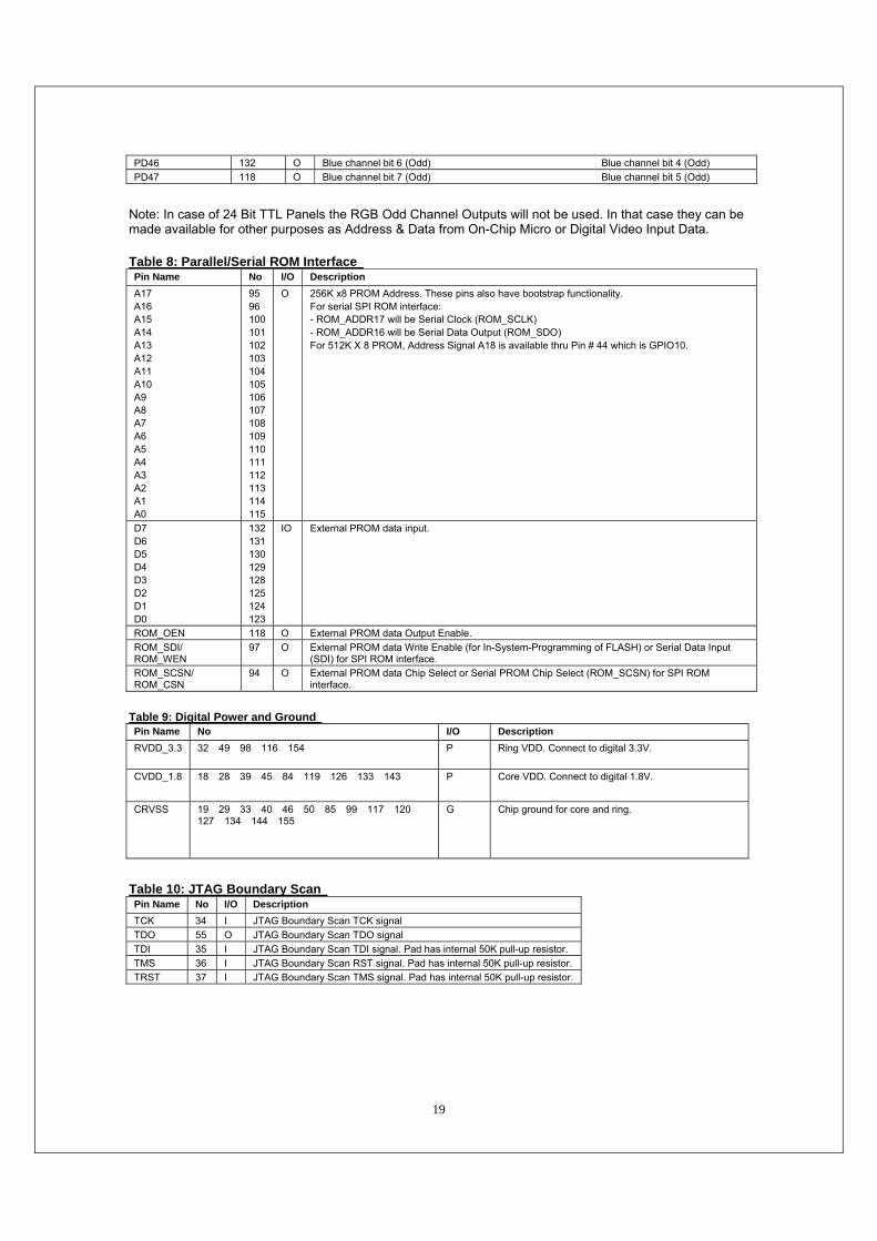
Note: In case of 24 Bit TTL Panels the RGB Odd Channel Outputs will not be used. In that case they can be made available for other purposes as Address & Data from On-Chip Micro or Digital Video Input Data. Table 8: Parallel/Serial ROM Interface Pin Name No I/O Description A17 A16 A15 A14 A13 A12 A11 A10 A9 A8 A7 A6 A5 A4 A3 A2 A1 A0
95 96 100 101 102 103 104 105 106 107 108 109 110 111 112 113 114 115
O 256K x8 PROM Address. These pins also have bootstrap functionality. For serial SPI ROM interface: - ROM_ADDR17 will be Serial Clock (ROM_SCLK) - ROM_ADDR16 will be Serial Data Output (ROM_SDO) For 512K X 8 PROM, Address Signal A18 is available thru Pin # 44 which is GPIO10.
D7 D6 D5 D4 D3 D2 D1 D0
132 131 130 129 128 125 124 123
IO External PROM data input.
ROM_OEN 118 O External PROM data Output Enable. ROM_SDI/ ROM_WEN
97 O External PROM data Write Enable (for In-System-Programming of FLASH) or Serial Data Input (SDI) for SPI ROM interface.
ROM_SCSN/ ROM_CSN
94 O External PROM data Chip Select or Serial PROM Chip Select (ROM_SCSN) for SPI ROM interface.
Table 9: Digital Power and Ground Pin Name No I/O Description RVDD_3.3 32 49 98 116 154 P Ring VDD. Connect to digital 3.3V.
CVDD_1.8 18 28 39 45 84 119 126 133 143 P Core VDD. Connect to digital 1.8V.
CRVSS 19 29 33 40 46 50 85 99 117 120 127 134 144 155
G Chip ground for core and ring.
Table 10: JTAG Boundary Scan Pin Name No I/O Description TCK 34 I JTAG Boundary Scan TCK signal TDO 55 O JTAG Boundary Scan TDO signal TDI 35 I JTAG Boundary Scan TDI signal. Pad has internal 50K pull-up resistor. TMS 36 I JTAG Boundary Scan RST signal. Pad has internal 50K pull-up resistor. TRST 37 I JTAG Boundary Scan TMS signal. Pad has internal 50K pull-up resistor.

20
4. CD4052B The CD4052B is a differential 4-Channel multiplexer having two binary control inputs, A
and B, and an inhibit input. The two binary signals select 1 of 4 pairs of channels to be turned on and connect the analog inputs to the outputs.
·PInputs
.
21
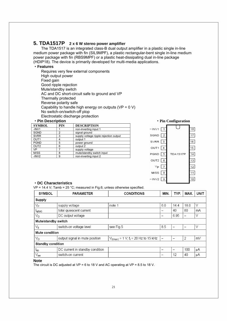
5. TDA1517P 2 x 6 W stereo power amplifier The TDA1517 is an integrated class-B dual output amplifier in a plastic single in-line
medium power package with fin (SIL9MPF), a plastic rectangular-bent single in-line medium power package with fin (RBS9MPF) or a plastic heat-dissipating dual in-line package (HDIP18). The device is primarily developed for multi-media applications. ·Features Requires very few external components High output power Fixed gain Good ripple rejection Mute/standby switch AC and DC short-circuit safe to ground and VP Thermally protected Reverse polarity safe Capability to handle high energy on outputs (VP = 0 V) No switch-on/switch-off plop Electrostatic discharge protection ·Pin Description ·Pin Configuration SYMBOL PIN DESCRIPTION -INV1 1 non-inverting input 1 SGND 2 signal ground SVRR 3 supply voltage ripple rejection output OUT1 4 output 1 PGND 5 power ground OUT2 6 output 2 VP 7 supply voltage M/SS 8 mute/standby switch input -INV2 9 non-inverting input 2 ·DC Characteristics VP = 14.4 V; Tamb = 25 °C; measured in Fig.6; unless otherwise specified.
Note The circuit is DC adjusted at VP = 6 to 18 V and AC operating at VP = 8.5 to 18 V.
22
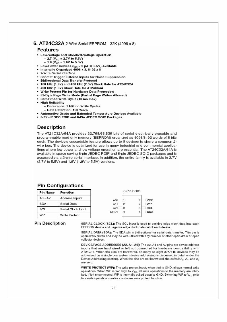
6. AT24C32A 2-Wire Serial EEPROM 32K (4096 x 8)
23
7. AT49BV040B
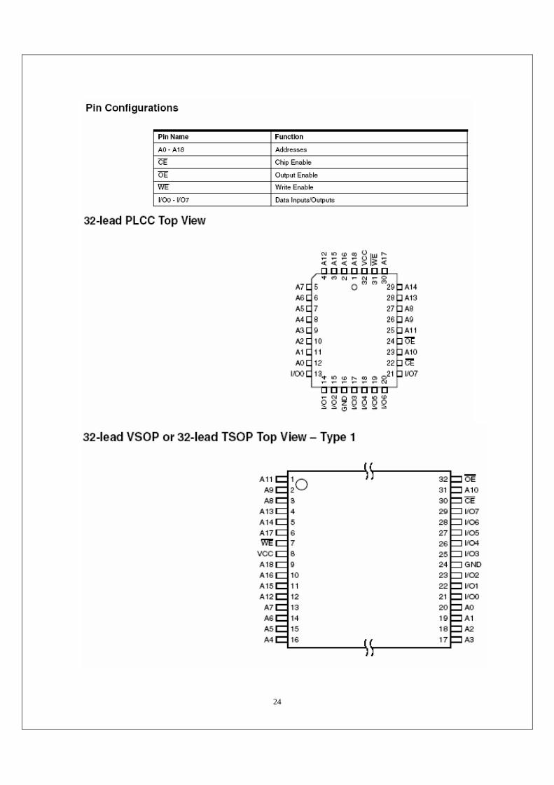
24

25
26
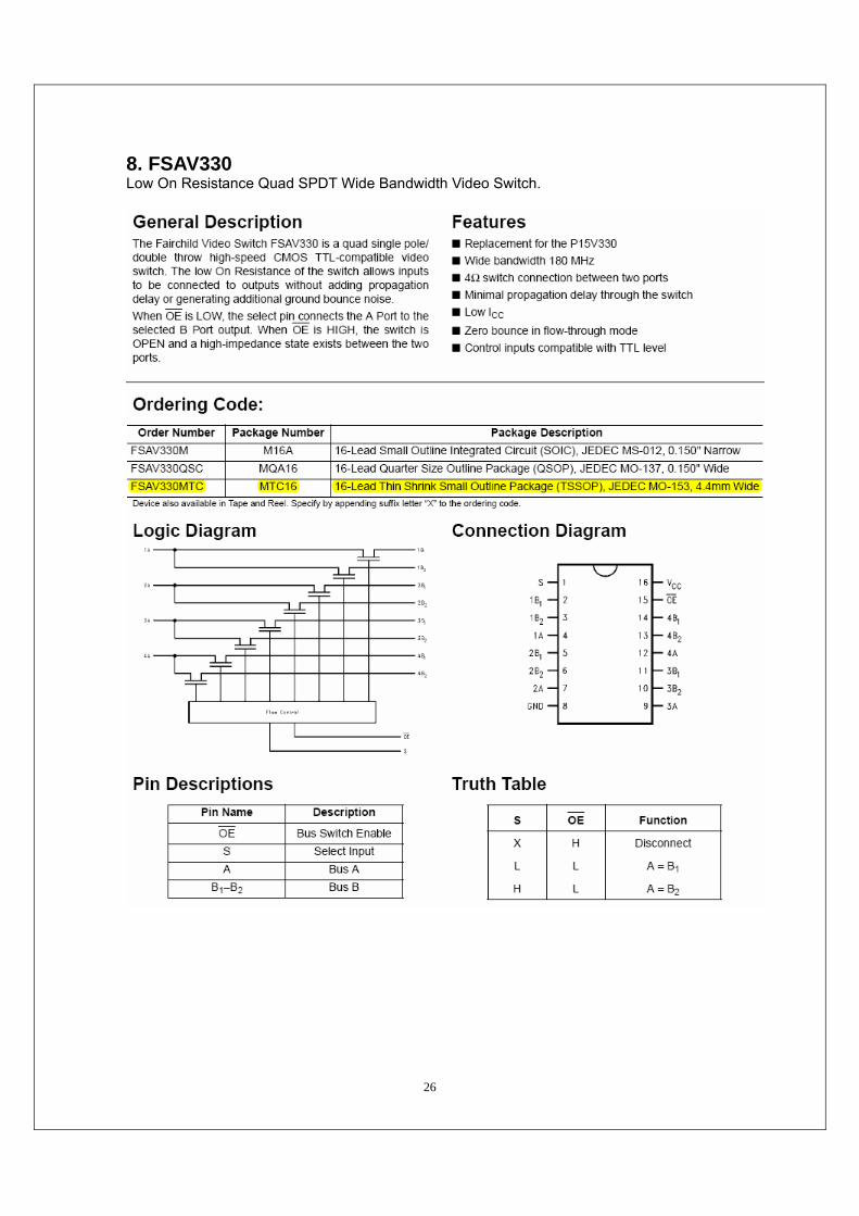
8. FSAV330 Low On Resistance Quad SPDT Wide Bandwidth Video Switch.

27
ICS ON HI-VOLTAGE BOARD 1. BIT3193 High Performance PWM Controller
BIT3193 integrated circuit provides the essential features for general purpose PWM controller in a small low cost 16-pin package. BIT3193 has built-in a low frequency PWM generator for any specified application. BIT3193 includes latched off protection feature may make the system more reliable while compare to other similar products. ·Features ·4.5V ~ 8V operation ·Fixed High Frequency, Voltage Mode PWM Control
·Latched Off Protection ·Build-In Low Frequency PWM Generator ·Build-in UVLO ·Low Power CMOS Process ·Totem Pole Output ·16 Pin Package ·Applications ·DC/DC Converters ·LCD TV ·LCD Monitor ·Notebook Computer ·Tablet PC ·Personal Digital Assistants ·Navigation Phone/ Door Phone ·Portable consumer product ·Recommended Operating Condition:
Supply Voltage 4.5~8V Operating Ambient Temperature 0~70 °C
Operating Frequency 50K~400K Hz
·Pin Layout: 1 16 INN MODSEL CMP ISEN LOAD CLAMP CTOSC PWMDC TIMER CTPWM ONOFF PWMOUT GND VDD NOUT2 NOUT1
8 9 ·Pin Description
Pin No.
Symbol I/O Descriptions
1 INN I/O The inverting input of the error amplifier. 2 CMP O Output of the error amplifier. 3 LOAD I/O A switch that connected to the high frequency triangle wave generator.
This switch is open while ISEN pin <1.3V. An external resistor connected here may change the operation frequency of CTOSC in open load situation.
28
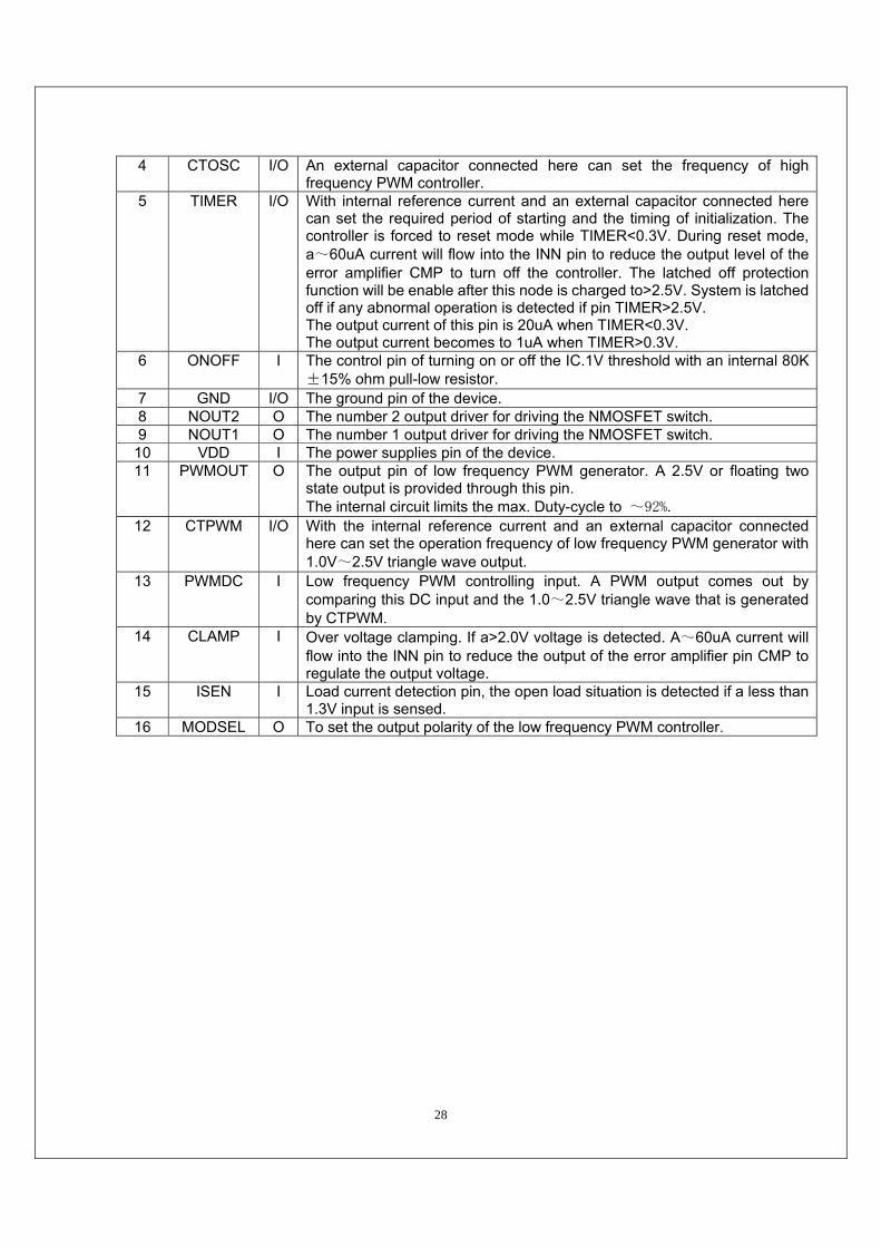
4 CTOSC I/O An external capacitor connected here can set the frequency of high frequency PWM controller.
5 TIMER I/O With internal reference current and an external capacitor connected here can set the required period of starting and the timing of initialization. The controller is forced to reset mode while TIMER<0.3V. During reset mode, a~60uA current will flow into the INN pin to reduce the output level of the error amplifier CMP to turn off the controller. The latched off protection function will be enable after this node is charged to>2.5V. System is latched off if any abnormal operation is detected if pin TIMER>2.5V. The output current of this pin is 20uA when TIMER<0.3V. The output current becomes to 1uA when TIMER>0.3V.
6 ONOFF I The control pin of turning on or off the IC.1V threshold with an internal 80K±15% ohm pull-low resistor.
7 GND I/O The ground pin of the device. 8 NOUT2 O The number 2 output driver for driving the NMOSFET switch. 9 NOUT1 O The number 1 output driver for driving the NMOSFET switch.
10 VDD I The power supplies pin of the device. 11 PWMOUT O The output pin of low frequency PWM generator. A 2.5V or floating two
state output is provided through this pin. The internal circuit limits the max. Duty-cycle to ~92%.
12 CTPWM I/O With the internal reference current and an external capacitor connected here can set the operation frequency of low frequency PWM generator with 1.0V~2.5V triangle wave output.
13 PWMDC I Low frequency PWM controlling input. A PWM output comes out by comparing this DC input and the 1.0~2.5V triangle wave that is generated by CTPWM.
14 CLAMP I Over voltage clamping. If a>2.0V voltage is detected. A~60uA current will flow into the INN pin to reduce the output of the error amplifier pin CMP to regulate the output voltage.
15 ISEN I Load current detection pin, the open load situation is detected if a less than 1.3V input is sensed.
16 MODSEL O To set the output polarity of the low frequency PWM controller.
29
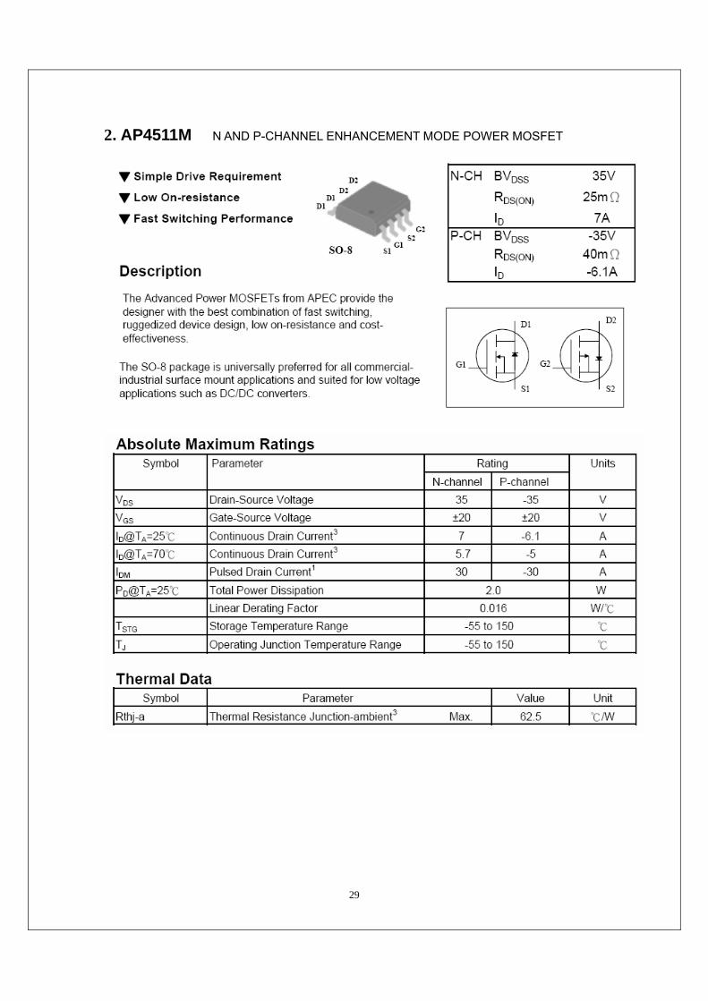
2. AP4511M N AND P-CHANNEL ENHANCEMENT MODE POWER MOSFET

30
Part 4 Detailed Circuit MAIN BOARD
1. Interface
GND
1R20
75
1C55
100n
12
4R81k
2R8
100R
2Q12N3904
1
23
VCC
1R27 47k
+
3EC610uF
IR-SW
AUDIO-SEL1
DISC_CHECK
2R7
0
IR
1L21
1L2047uH/2A
R
AUDIO-SEL0
1C3 100nF
4R1470
LED_G
3R54100K
H_SYNC1
VCC5
VCC16
DVD_CHECK
+
3EC3100u25V
VGA_SCL
1R775R/1%/NC
GND
DVD-PB
2C34
22P
12
2R54.7K
1R12
GIN2
IR-SW
1R24 2.7k
3R53100K
OUT_LVGA-R
GND
VCC5
GIN2
LED_G
GND
GND
+
3EC1410uF
1R21 2.7k
GND
LED_G
GND
+
1EC2
+
3EC510uF
RIN1
VCC8
BIN2
LED_R
VCC
VGA-R
1L1 FB
R0603--
VCC16
DVD_CHECK
1R17
GND
1CON31234
1234
5U1PESD5V0L5
1
2
3456
3R1100K
VGA_SCL
CVBS1
GND
4052-L
GND
DVD_CHECK
GIN1
CVBS1
4052-R
3R61
10K
LED_G
DVD-CVBS
3R58
10K
1R9
75R/1%/NC
1C10
1 2 VGA-L
BIN2
1C46
100n
1 2
AV_L
DVD-Y
4R41k
+
3EC1210uF
4052-R
LED_R
PR
AV_R
V_SYNC1
1R320
YPbPr_L
SP_LOUT
3U1HEF4052SOP16
1
2 34
5
6
7 8
91011
12 131415
16
0Y
2Y Y_OUT3Y
1Y
INH VEE
GN
D BA3X
0X X_OUT1X2X
VC
C
VCCGNDSWADJ
VCC5
3R12 100R
1R8
75R/1%/NC
SP_LOUT
DVD_L
1R28 47k
1R18
75
4052-L
VCC
4052-R
GIN1
IR
1C522pF/NC
+5V
1R23 2.7k
+
3EC1010uF
DVD-IR
4R31k
5U2
PESD5V0L5
1
2
3456
DVD-Y
+1EC1100u16V
SVH-Y
RIN2
1U1FSAV330TSSOP16
14
25
11
36
1013
1
8
15
47912
16
4B1
1B12B13B1
1B22B23B24B2
S GN
D OE
1A2A3A4A
VCC
CVBS-OUT
4052-L
VCC5
SVH-C
3R59
10K
3C1100nF
2R4100
BIN1
GND
1L2
3R2100K
+5V
H_SYNC1
RIN1
1R26 47k
1R575R/1%
LED_G
VGA_SDA
4R210k
GND
5C2100n
1 2
GND
1Q1
2N3904
1
23
5D1BAV99
3
21
+5V
4052-R
YPbPr_R
DVD-IR
IR1C2 100nF
4052-R
8125IR
DVD-PR1CON1
1234567891011
123456789
1011
1R22 2.7k
3R3100K
1C47
100n
1 2
VGA_SCL
DISC_CHECK
AV_L
2Q22N3904
1
23
1R120
1R13
75
到背光板
3R57
10K
AUDIO-SEL0
DVD_R
1R220
1CON4
12345
RIN2
IR-SW
5CON2
12
3EC4100uF/16V
4Q2
2N3904
1
23
VCC8
DVD_CHECKDVD-PR
1R10
10K
3R5
10K
3R4100K
4R610k
3C11100pF
VCC5_STB
Y
1C8
1 2
1C4 100nF
GND
3R710K
VCC16
3C3100n
12
3R6
10K
4052-L
VCC5GND
PB
RIN2
V_SYNC1
1R57
75R/1%/NC
AUDIO-SEL1
GND
DVD-PB
YPbPr_R
3R56100K
1CON51234567891011
123456789
1011
OUT_L
3EC1100uF/16V
3C5
100pF
NC
4Q3
2N3906
1
23
4R5470
3R55100K
OUT_ROUT_L
DVD_CHECK
8125IR
IR
LED_G
1C53
100n
12
1R15
Value = 20
SP_ROUT
OUT_R
2R1100
1C59
22pF/NC
GNDCON7-2
12345678
12345678
3C8
100pF
DVD_R
VGA_SDA
1R11
10K
DVD
VCC5_STB
DVD_CHECK
1CN3A
AUX
12345
GNDY-ALV-AR
NCNC
LED_R
SVH-C
SVH-Y
BACK_EN
GND
3R11 100R+
1EC3
BIN2
1C9
1 2
1C48
100n
1 2
+5V
IR
VCC16
1CN1B
AUX2
1
2
34
5
1CN2A
AUX
531
98
7246
PRPBY
GNDGND
GNDY-LY-RNC
SVH-Y
1L4
CVBS-OUT
3C9100pF
+
1EC5
GND
GIN2
1C722pF/NC
+5V
Y
CVBS1
VCC8
1R675R/1%
3R8
10K
VCC5
VCC5
GIN1
GND
DISC_CHECK
RIN1
1R14
DVD
VCC5_STB
OUT_R
AV_R
1C54
100n
12
3R1010K
4R71k
GND
1R475R/1%
1R16
75
3CON1
12345
1C1
100nF
IR-SW
VGA-L
8125IR
3R910K
+
1EC4
2.2uF/16V
GND
4Q1
2N3906
1
23
1R25 47k
YPbPr_L
1CN1A
AUX2
6
7
89
L
VCC5
GND
2R310K
AUDIO-SEL0
3C10100pF
3Q1
2N39041
23
BACK_EN
3R62
10K
3C4100nF
AUDIO-SEL1
H_SYNC1
1CON212345
12345
5CON1
12
+5V
BACK_PWM
BACK_EN
3L2
2C35
22P
12
3L1
2R610K
1L3
VGA_SDA
BACK_PWM
V_SYNC1
SP_ROUT
1R19
75
1C56
100n
12
SVH-C
3Q22N3904
1
23
3C6
100pF
LED_RIR-SW
PB
4052-L
+5V
VCC8
BIN1
LED_R
8125IR
GND
2R24.7K
3R60
10K
4Q42N3904
1
23
IR
PR
BIN1
DVD_L
GND
1C622pF/NC
+
3EC910uF
5C1100n
12

31
2. Hundson VCC3.3 DVD_CHECK
SCART-CVBS
2C46100n
12
1L22 10u
2C15100n
12
2C50100n
12
2C32100n
12
IR
D2
GND
2C48100n
12
2C25100n
12
2C23100n
12
VCC1.8
A1
GND
+ 2EC1
47u16V
2C21100n
12
2C20100n
12
+2EC1647u16V
2C39100n
1 2
2R58 01 82 73 64 5
POWER_ON
A9
A14
2C5100n
12
2C22100n
12
A8
MU
TE
GIN2
A16D3
2R16 10k
2R28
0NC
LED_G
SCART-R
RESET-TV
SLEEP
D5
2C52100n
12
2R50
75
2C45100n
12
2R2620
RIN1
A6
A13
+2EC5100uF16V
AUDIO-SEL0
RESET-TV
CVBS0
2R23 10k
+1.8V_RPLLH_SYNC1
LED_R
A4
A0
VCC5
2L15
2C37100n
12
BIN2
A11
2L7
CVBS1
LED_G
2R48
75
IR-SW
1POWER_ON
A10
VCC1.8
SLE
EP
VCC3.3_PANEL
D3
D5
2R92.7k
2R53
100
CVBS0
SCART-G
2R49
75
2R102.7k
2R2720
2R51
75
A182R18 10k
2L11
SVH-C
GIN12R4410k
VCC5
+3.3V_RPLL
CVBS-OUT
2C47100n
12
ADC_IN1
PANEL_ON
D0
8125IR
IR-SW
SCART-R
SCART-SW
POWER
A1
D2
VCC3.3
ROM_OEN
H_SYNC1
SCART-G
DISC_CHECK
+2EC347u
16V
V_SYNC1
A16D7
IR-SW
2C7100n
12
2R57 01 82 73 64 5
VCC3.3_PANEL
CVBS0
ADC_IN2
1PO
WER
_ON
2R5210k
+3.3V_I/O_HUDSON
VCC3.3
DVD_CHECK
+2EC11
47u16V
+1.8V_CORE
LED_R
2R41100
2C4
100n
12
BACK_EN
SCL2CON2
1234
+2EC1047u16V
2C53100n
12
IR
2C9100n
12
GIN1
A4
2R13 4.7k/NC
+3.3V_I/O_HUDSON
ADC_IN1
A17
V_SYNC1
A3
A12
2R4510k
2C29100n
12
+2EC15100uF16V
+3.3V_LBADC
2R374.7k/NC
BACK_EN
2R42100
RIN2
A17
AUDIO-SEL0
2R19 10k
+3.3V_RPLL
CVBS-OUT
8125IRAUDIO-SEL1
DVD_CHECK
A6
A15
2R39100
2U1AT49BV040B
3
29 28
4
25 232627
5 6 7 8 9 10 11 1221
20191817
1514
132224
3132
116
30
2
A15
A14
A13
A12
A11
A10A9A8
A7
A6
A5
A4
A3
A2
A1
A0
DQ
7
DQ6DQ5DQ4DQ3
DQ2DQ1
DQ
0C
E#
OE#
WE#VCCA18
VSS
A17
A16
+3.3V_I/O_HUDSON
GND
ROM_CSN
A14
A3
SC
ART-
FB
BIN1
D7
VGA_SDA
A14
A7
+2EC447u16V
SVH-C
SCL
D1
2C26100n
12
VCC5BACK_PWM
2R29
+2EC7100uF16V
8125IR
SCART-G
+2EC17100UF16V
ADC_IN3
+2EC13220uF16V
2L1
2R432.2k
SCART-FB
H_SYNC1
A12
+3.3V_LVDS
A10
ROM_WEN
RIN2
RIN2
DISC_CHECK
A17
LED_R
A5
SCART-B
A0
A18
2R14 4.7k
2R30
2R59 01 82 73 64 5
2C43100n
12
GND
DVD_CHECK
CVBS1
RIN1
A13
+ 2EC1910u16V
2C13100n
12
2C42100n
1 2
2C5830p
VCC3.3_PANEL
SCL
VCC3.3_PANEL
2Y1
19.6608M
2R3220
SCL
2R12 10k
2L8
2C55100n
12
VCC1.8
SCART-R
ADC_IN1
2C33100n
12
+1.8V_RPLL
VCC5
+1.8V_ADC
1POWER_ON
IR
RIN1
VCC3.3
2R2520
VCC3.3
BACK_PWM
SCART-CVBSSDA
AU
DIO
-SEL
0
DISC_CHECK
BIN1
A2
2L9
A8
SC
ART-
SW
+2EC1247u16V
2C11100n
12
2R3320
VGA_SDA
SCART-B
2R15100
2C24100n
12
2L5
2R310
VCC5
A9
2C28100n
12
2C1100n
1 2
2C5730p
A7
A15
2R54100
+1.8V_CORE
VCC5
2C12100n
12
PANEL_ON
1POWER_ON
SVH-Y
2R3410k/NC
SDA
VCC3.3
SCART-FB
A8
POWER_ON
+2EC647u16V
2C51100n
12
2C31100n
12
2C8100n
12
2C27100n
12
2C3
100n
12
GIN2
A11
2C54100n
12
+2EC1847u16V
+3.3V_LVDS
VCC5
LED_G
2R360
2C49100n
12
2C2100n
1 22R20 10k
ROM_CSN
2R3510k/NC
2Q42N3904
1
23
2C56100n
12
SVH-Y
D6
A13
VGA_SCL
ADC_IN3
D1
A9
2C38100n
12
VCC3.3
2U2
24LC32SN
1234 5
678A0
A1A2VSS SI
SCKWP
VCC
2R17100
SVH-C
ADC_IN2
A2
2Q32N3904/NC
1
23
SCART-B
PANEL_ON
BACK_PWM
GIN1
2C19100n1 2
2R5675R/1%/NC
SVH-Y
2C44100n
12
+1.8V_ADC
VCC5
VCC3.3
2R22 10k
2L6
2R11 10k
2C16100n1 2
2C14100n
12
2C17
100n12
2R24 22
1 82 73 64 5
VCC3.3
MUTE
CVBS-OUT
+
2EC247u16V
MUTE
CVBS-OUT
VCC5
BIN1
SDA
VCC5
2U3
FLI8125
9 10 11 13 14 15 16 20 21 22 23 24 25 26 272 3 4 5 6 7 8 4033291912 45392818 32 491 17 30 31 34 35 36 37 38 41 42 43 44 47 48 51 5246 50
180181182183
151
152
153
154
155
156
150
149
148
147
146
145
144
143
142
141
140
139
138
137
136
135
134
133
132
131
130
129
128
127
105
106
107
108
109
110
111
112
113
114
115
116
117
118
119
120
121
122
123
124
125
126
5354555657585960616263646566676869707172737475767778798081828384858687888990
9291
93949596979899100101102103104
169168167166165164163162161160159158157
179178177176175174173172171170
208207206205204203202201200199198197196195194193192191190189188187186185184
VSSA
33_L
BAD
CR
ESET
nG
ND
_RP
LL
VBU
FC_R
PLL
AGN
D_R
PLL
XTAL
TCLK
STI_
TM2
GPI
O15
/ST
I_TM
1/EX
T_C
SSY
NC
2VS
YNC
2H
OS
T_SC
L/U
ART_
DI/J
TAG
_CLK
HO
ST_
SDA/
UAR
T_D
O/J
TAG
_MO
DE
DD
C_S
CL
DD
C_S
DA
LBAD
C_I
N1
LBAD
C_I
N2
LBAD
C_I
N3
LBAD
C_I
N4
LBAD
C_I
N5
LBAD
C_I
N6
LBAD
C_R
TN
RVS
S
RVS
S
RVS
S
RVS
S
VDD
_RPL
L_18
CVD
D_1
8
CVD
D_1
8
CVD
D_1
8
CVD
D_1
8
RVD
D_3
3
RVD
D_3
3
VDD
A33_
LBAD
C
AVD
D_R
PLL
_33
I2C
M_S
CL
I2C
M_S
DA
GPI
O0/
LED
1/T
CK
GPI
O1/
LED
2/T
DI
GPI
O2/
PWR
_CT
RL/
TMS
GPI
O3/
SCAR
T16
_1G
PIO
6/IR
in
GPI
O7/
IRQ
inG
PIO
8/IR
Qou
tG
PIO
9/SI
PC_S
CL
GPI
O10
/SIP
C_S
DA/
A18
GPI
O11
/PW
M0
GPI
O12
/PW
M1
GPI
O13
/PW
M2/
VBI_
VALI
DG
PIO
14/P
WM
3/SC
ART
16_2
RVS
S
RVS
S
B2PGNDSC2PAVDD_B
VID
_D14
/VID
1_14
/GP2
2VI
D_D
15/V
ID1_
15/G
P23
VID
_CLK
_1/V
ID1_
CLK
RVD
D_3
3R
VSS
HSY
NC
1
VID
_D13
/VID
1_13
/GP2
1VI
D_D
12/V
ID1_
12/G
P20
VID
_D11
/VID
1_11
/GP1
9VI
D_D
10/J
TAG
_TD
I/VI
D1_
10/G
P18
VID
_D9/
JTA
G_T
DO
/VID
1_D
9/G
P17
VID
_D8/
JTR
ST/V
ID1_
D8/
GP
16R
VSS
CVD
D_1
8VI
D_D
7/VI
D1_
D7
VID
_D6/
VID
1_D
6VI
D_D
5/VI
D1_
D5
VID
_D4/
VID
1_D
4VI
D_D
3/VI
D1_
D3
VID
_D2/
VID
1_D
2VI
D_D
1/VI
D1_
D1
VID
_D0/
VID
1_D
0R
VSS
CVD
D_1
8VI
D_D
IN23
/D7/
PD
46/V
ID2_
7VI
D_D
IN22
/D6/
PD
45/V
ID2_
6VI
D_D
IN21
/D5/
PD
44/V
ID2_
5VI
D_D
IN20
/D4/
PD
43/V
ID2_
4VI
D_D
IN19
/D3/
PD
42/V
ID2_
3R
VSS
VBI
_D7/
A10/
PD34
/BT2
VBI
_D6/
A9/
PD33
/BT1
VBI
_D5/
A8/
PD32
/BT0
VBI
_D4/
A7/
GP
IO23
/PD
31V
BI_D
3/A
6/G
PIO
22/P
D30
VBI
_D2/
A5/
GP
IO21
/PD
29V
BI_D
1/A
4/G
PIO
20/P
D28
VBI
_D0/
A3/
GP
IO19
/PD
27VB
I_VA
LID
/A2/
GP
IO18
/PD
26VB
I_C
LK/A
1/G
PIO
17/P
D25
VID
_DE/
FLD
/A0/
GP
IO16
/PD
24R
VDD
_33
RVS
SVI
D_C
LK2/
RO
M_O
EN/P
D47
/VID
2_C
LKC
VDD
_18
RVS
SG
PIO
5/VI
D_V
S/V
ID2_
VS/
VID
1_VS
GPI
O4/
VID
_HS/
VID
2_H
S/V
ID1_
HS
VID
_DIN
16/D
0/P
D39
/VID
2_0
VID
_DIN
17/D
1/P
D40
/VID
2_1
VID
_DIN
18/D
2/P
D41
/VID
2_2
CVD
D_1
8PBIASPPWR
BSCAN_TDOAVDD_LV_33
VCO_LVAVSS_LV
AVDD_OUT_LV_33CH3P_LV_E/R0CH3N_LV_E/R1CLKP_LV_E/R2CLKN_LV_E/R3CH2P_LV_E/R4CH2N_LV_E/R5CH1P_LV_E/R6CH1N_LV_E/R7CH0P_LV_E/G0CH0N_LV_E/G1AVSS_OUT_LV
AVDD_OUT_LV_33CH3P_LV_O_G2CH3N_LV_O_G3CLKP_LV_O_G4CLKN_LV_O_G5CH2P_LV_O_G6CH2N_LV_O_G7CH1P_LV_O_B0CH1N_LV_O_B1CH0P_LV_O_B2CH0N_LV_O/B3AVSS_OUT_LV
AVDD_OUT_LV_33CVDD_18
RVSSPD20/B4PD21/B5PD22/B6PD23/B7
DEN/VOP_FLD
DVS/VOP_VSDHS/VOP_HS
DCLK/VOP_CLKROM_SCSN/ROMCSN
ROM_SCLK/A17/OSC_SELROM_SDO/A16/OCM_ROM
ROM_SDI/ROM_WENRVDD_33
RVSSEXT_ADC_CLMP/A15/SPI_EN
XOSD_CLK/A14/PD38/OP_MD1XOSD_HS/A13/PD37/OP_MD0
XOSD_VS/A12/PD36/JT_BSCANXOSD_FLD/A11/PD35/ROM512K
GNDSA1PGNDSSV1PAGNDAGNDAVDD_ADCADC_TESTVDD18_CGND18_CNCVDD18_ABVSYNC1
GNDSA2PGNDSSV2PAGNDANAVDD_AC1PGNDSB1P
GND18_SCVDD18_SCVOUTVO_GNDSVNAVDD_SCC4PGNDSB4PGNDSA4PGNDSSV4PAGNDCNAVDD_CC3PGNDSB3PGNDSA3PGNDSSV3PAGNDBN
VGA_SCL
ROM_OEN
2R38
0
POW
ER
_ON
2R55
690
2C40
100n
12
2L3
2R46100
2L2
AU
DIO
-SEL
1
D0
2L10
2C10100n
12
AUDIO-SEL1SLEEP
A11
DVD
_CH
ECK
SCART-SW
D4
2C41
100n
12
D6
2R21 10k
IR
BIN2
CVBS1
SDA
PO
WER
A5
ADC_IN2
2L13
BIN2
GIN2
V_SYNC1
2L4
2C6100n
12
POWER A12
2R403.3k
RES
ET-T
V
SCART-CVBS
SCART-FB
DVD-CVBS
2C30100n1 2
+
2EC2047u16V
1POWER_ON
CVBS-OUT
+2EC9100UF16V
2R47100
VCC3.3_PANEL
VGA_SCL
A16
VGA_SDA
BACK_EN
ROM_WEN
A10
+2EC847u16V
TO
P
2CON1LVDS20
123456789
1011121314151617181920
2L12
+3.3V_LBADC
A15
ADC_IN3
D4
2C18
100n12
32
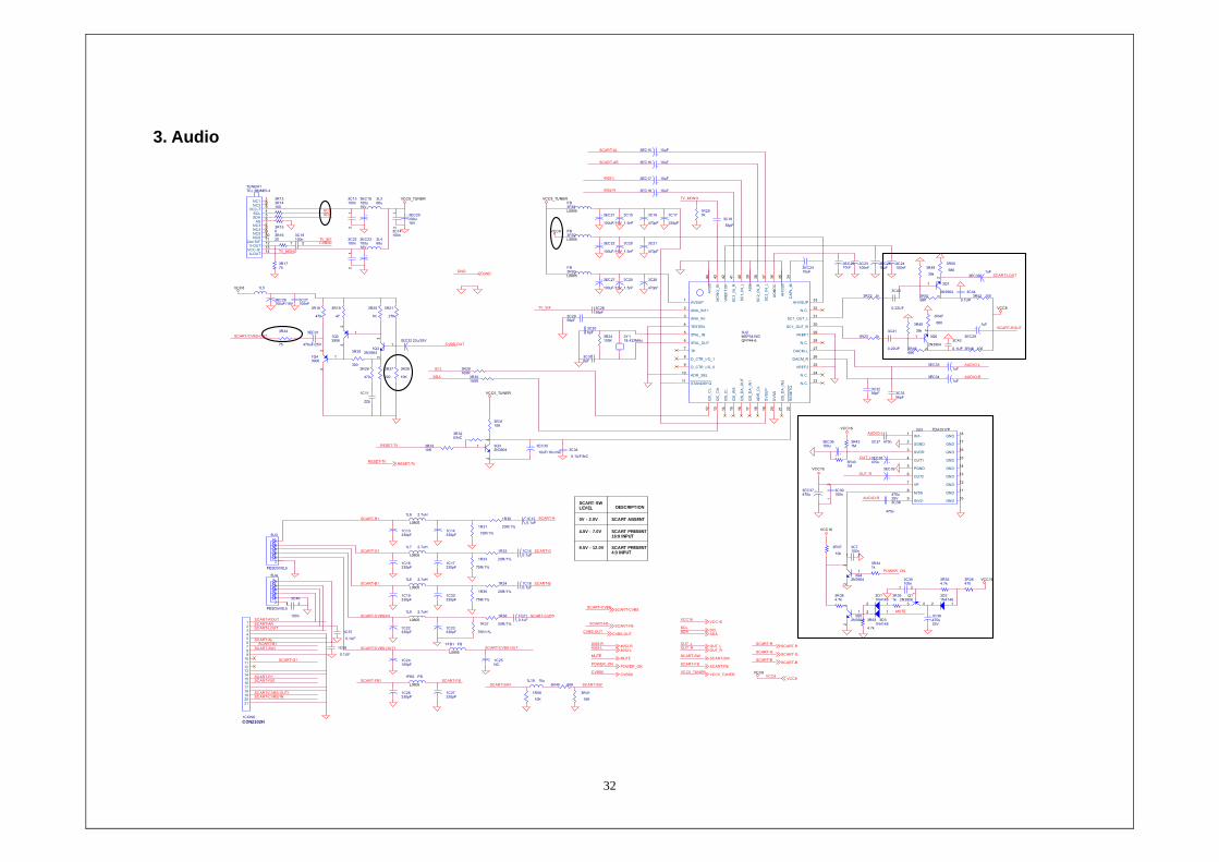
3. Audio
SCART-CVBS
OUT_L
SCART-AL
3R47
680
+ 3EC21
100uF/16V
SCART-SW LEVEL
OUT_R
VCC8
AUDIO-R
1L8 2.7uH
L0805
1C58
0.1UF
SCART-CVBS
3Q7
2N3904
1
23
4.5V - 7.0V
SCART-R
3C15
1.5nF
1R34
20R/1%
+3EC38470u
VCC8
POWER_ON
SCART-LOUT
+
3EC23100u16V
9.5V - 12.0V
3C306pF
1C180.1uF
4052-L
3FB1FB
L0805
SCART-CVBS/IN
VCC5_TUNER
AUDIO-R
3R37
10k
3C13100n
12
3C14100n
12
SCART-B1C24100pF
SCART-SW
1FB1 FB
L0805
SCART PRESENT4:3 INPUT
4052-R
TV_MONO
RESET-TV
3EC2610uF
1C26330pF
1C16330pF
3R27
220
VCC5_TUNER
SCL
SCART-CVBS/IN
VCC16
3R41
10K
+ 3EC27
100uF/16V
SCART-FB
SCL
1C13330pF
3C42
0.1UF
3C44
0.1UF
3C23100nF
1C11
22p
3R320/NC
3R25
300
VCC16
OUT_L
SCART PRESENT16:9 INPUT
VCC8
1R35
75R/1%
3R19
47
CVBS0
SCART-G
3R20
1K
3C21
470pF
+
3EC29
1uF
3C24100nF
Q12N3906
1
23
3D21N4148
2 1
1R30
20R/1%
SCART/CVBS-OUT1
1C210.1uF
SCART-FB
3C25
1.5nF
1R32
20R/1%
+ 3EC35
10uF/16v /NC
3R23 1k
SCART-CVBS
+
3EC36100u
1CON6CON2102H
123456789
101112131415161718192021
VCC5_TUNER
3R354.7k
+ 3EC20100u16V
TV_SIF
SCART-FB
OUT_R
3R44
75
1C25NC
VCC16
1R56
10K
1L7 2.7uH
L0805
1L5
3R29100R
1Q43906
3
1
2
3R63
4.7k
SCART/CVBS-OUT
3C316pF
1C19330pF
+3EC301uF
SCART-R
SCART-SWI
1L6 2.7uH
L0805
1R37
75R/1%
SCART-B
TV_SIF
3D31N4148
2 1
SCART-SW
GND
MUTE
SCL
3R3310K
+3EC16 10uF
+3EC331uF
3R22 1k
3R431M
5U3
PESD5V0L5
1
2
3456
VCC16
4052-R
SCART-AR
3R45
39k
SCART-B1
3FB3FB
L0805
3C39100n
12
3FB2FB
L0805+ 3EC22
100uF/16V
3C35100n
1 2
1C22330pF
CVBS0
SCART-ROUT
3C2856pF
3R3110K
VCC16
1C14330pF
1C20330pF
TV_MONO
4052-R
+3EC18 10uF
5U4
PESD5V0L5
1
2
3456
1C23330pF
SCART ABSENT
4052-L
AUDIO-L
SCL
SCART-SW
3R4668k
3R18
470
SCART-FB1
SCART/CVBS-OUT
3U2MSP3415GQFP44-6
2
3
43 4041 373839
11
10
1312 15 17 2114 16
27
26
31
30
9
8
4
42 36
5
6
34
29
25
20
3544
28
32
24
23
2219
331
7
18
ANA_IN1+
ANA_IN-
MO
NO
_IN
SC1_
IN_L
SC
1_IN
_R
SC2_
IN_L
SC
2_IN
_R
AS
G
STANDBYQ
ADR_SEL
I2C
_DA
I2C
_CL
I2S
_WS
I2S
_DA
_IN
1
I2S
_DA
_IN
2
I2S
_CL
I2S
_DA
_OU
T
DACM_L
DACM_R
SC1_OUT_L
SC1_OUT_R
D_CTR_I/O_0
D_CTR_I/O_1
TESTEN
VR
EF
TO
P
AG
ND
C
XTAL_IN
XTAL_OUT
CA
PL_
M
VREF1
VREF2
DV
SS
AH
VS
S
AV
SS
N.C.
N.C.
N.C.
N.C.
RE
SE
TQ
DV
SU
P
AHVSUPAVSUP
TP
AD
R_C
L
OUT_R
3Q6
2N3904
1
23
1C27330pF
SCART-G
3R21
27K
3C19100n
1 2
0V - 2.0V
SCART-B
3EC2510uF
SCART-SWI
SCART-G1
3C2956pF
3R52 100
1C17330pF
VCC8
3C27100nF
3C20
1.5nF
3C17
220pF
SCART-FB
3R341k
3R13
100
1Q23906
3
1
2
SCART-R1
SCART-FB1
POWER_ON
3R48 100
3R49
39k
3L468u
3R24100K
3R1775
3R30100R
SCART-G
VCC8
MUTE
3R26
470
3C40
100n
1 2
3EC32 22u/25V
1R291K
+3EC15 10uF
3R150
4052-L
POWER_ON
DESCRIPTION
VCC16
RESET-TV
SCART-R1
VCC5_TUNER
CVBS0
+3EC341uF
CVBS-OUT
CVBS-OUT
1R33
75R/1%
+
3EC19100u16V
SDA
3L368u3R14
SCART-B1
3C22100n
12
3C38
470n
CVBS-OUT
SCART-AL
SCART/CVBS-OUT1
3EC2410uF
3U3 TDA1517P
2
1
3
4
5
6
7
8 11
12
13
14
15
16
17
18
9 10
SGND
IN1-
SVRR
OUT1
PGND
OUT2
VP
M/SS GND
GND
GND
GND
GND
GND
GND
GND
INV2- GND
3R5168k
3C26
470pF
3Q42N3904
1
23
3C7100n
1 2
3C43
0.22UF
MUTE
SCART-ROUT3EC31
470uF/25V
3C41
0.22UF
3R36470
SCART-FB
3C3356pF
1R36
20R/1%
3R40 30K
SDA
OUT_L
3R391k
SCART-R
AUDIO-L
SCART-LOUT
3C34
0.1UF/NC
SCART-G1
3R421M
TUNER1TCL MNM05-4
1234567891011121314
NC1NC2
VCC-TSCLSDA
ASNC3NC4NC5NC6
2nd SIFV-OUT
VCC-IFA-OUT
+
3EC39
470u25V
3R384.7k
1L9 2.7uH
L0805
1FB2 FB
L0805
RESET-TV
SDA
VCC8
1R31
75R/1%
+ 3C36470u25V
SCART-AR
+3EC37470u
3C3256pF
3C16
470pF
3R28
10K
1C57
0.1UF
3C18
56pF
VCC5_TUNER
GND
3Y118.432MHz
+3EC17 10uF
3EC28100uF/16V
3Q52N3904
1
23
SDA
1C150.1uF
1C120.1uF
3R50
680
3Q32N3904
1
23
3D11N4148
2 1
3R1620
1Q32N3904
1
23
3C37 470n
1L19 10u

33
4. Power
VCC3.3
1POWER_ON
1U5 FDS94351234 5
678
S1S2S3G D4
D3D2D1
LED_G
IR
GND
LED_G
1U4AIC1117-1.8
1
3 2
GNDVIN OUT
VCC16
+1EC7100u25V
+
1EC11100u16V
4R280/NC
1POWER_ON
GND
4R123.3k
4R29 100/NC
1L16 10u
GND
GND
1R442k
4R19 0/NC
GND
+1EC18
100u16V
VCC16
VCC8
ADC_IN1
VCC5
2L16
4R21 0/NC
4R163.3k
1JP1
DC12V-IN1
2 3
1C60
104
4R20 100/NCVCC3.3_PANEL
IR
GND
GND
1C50
100n12
3L5
VCC3.31R4610k
1C41100n
12
VCC1.8
1C32100n
12
1C36100n
12
LED_R
1R5310k
IR
LOW LEVEL ON
8U1L7808
1 3
2
IN OUT
G
VCC5_STB
VCC16
ADC_IN1
+1EC17100u/NC16V
VCC5
VCC
+
1EC14100u16V
VCC5
PANEL_ON
VCC16
GND
LED_R
1R51100
1R431.2kVCC3.3
VCC5_STB
+
4EC1100u25V
ADC_IN3
4R94.7k
KEY_ADC_IN3
+1EC19100u25V
1Q72N3904/NC
1
23
1CON8
12345
LED_G
VCC5_STB
IR
1L17 10u
2D1
HZ5V1
12 ADC_IN2
PANEL_ON
GND
1U3
AP1513
1234 5
678
FBENOCSETVCC OUT1
OUT2VSS1VSS2
GND
4R25 100/NC
1CON7123456
123456
VCC16
GND
ADC_IN3
1Q62N3904
1
23
1C42100n
12
1R55
10k
1Q52N3904
1
23
1R383.3k
LED_G
IR
1L15
GND
VCC3.3
POWER
4R244.7k/NC
1C30100n
12
2L14
ADC_IN3LED_R
4R18100/NC
VCC3.3_PANEL
VCC3.3_PANEL
GND
GND
4R224.7k/NC
1U2
AP1510
1234 5
678
FBENOCSETVCC OUT1
OUT2VSS1VSS2
1POWER_ON
1C29100n
12
SLEEP
1L18 10u
VCC16
1R413k
1R4010k
4R17 100/NC
3D8 HZ5V11 2
PANEL_ON
ADC_IN2
1C35100n
12
POWER_ON
1C51
100n12
1R45100k
+
1EC9100u16V
VCC3.3
4R134.7k/NC
4R234.7k/NC
VCC5
+1EC16100u16V
1L1147uH/2A
GND
4R27 100/NC
1R471.8k
1C28
104
GND
1C52
100n12
POWER_ON
VCC
1C45100n
12
1C43100n/NC
12
4R260/NC
+
1EC6100u25V
1R39100k
4R104.7k
1C3710n
VCC8
VCC5_TUNER
1R5410k/NC
VCC5
VCC8POWER_ON
1C40100n
12
1C33
100n 12
ADC_IN2
4R154.7k/NC
LED_R
VCC5
1L13
ADC_IN1
+1EC10100u25V
LED_G
POWER
1L10
VCC1.8
VCC5_STB
SLEEP
1L1233uH/2A
1C39100n
12
+
1EC8220u16V
1R481.2k
1C38100n
12
4R114.7k
1L14
1U7FDS9435
12345
678 S1
S2S3GD4
D3D2D1
VCC5_STB
1C3110n
4U1
ATTINY12L
12345
678 PB5
PB4PB3
GNDPB0PB1PB2VCC
IR
+
1EC15100u16V
1D2SS23
21
VCC1.8IR
1C49
100n12
1R5010k/NC
VCC16
+
1EC13220u16V
+1EC12100u16V
VCC16
1D1SK34
21
1R52100/NC
GND
VCC8
4R300/NC
1R42
10k
1C34100n
12
VCC5
VCC5_TUNER
KEY_ADC_IN3
1C44100n
12
4R144.7k/NC
1R4910k
1U6 FDS9435/NC1234 5
678
S1S2S3G D4
D3D2D1
KEY_POWER
SLEEP
VCC5_TUNER
VCC
GND
VCC16
POWER
LED_R
GND

34
HI-VOLTAGE BOAD
Q12N3904
R19103
R20
103
C3106
D6
1SS355
R17474
BAV99
CR2
13
2
Q3
2N3904
C25104
BAV99
CR3
13
2
C24
105
R9104
Q52N70022
31
J1
PH05-2A
12345
R13
153
R18203
D5
1SS355
C11
222
C7223
R3
202
C18222
T21 8
5 7
C14
821
R5
223
R22203
R23
103
R7683
C26104
R4681
OP1
R15683
T1
1 8
5 7
R8
103
F1
3A
BAV99
CR4
13
2
J2
8.0-2A
1
2
R21203OP2
C20NC
NIA19LES018
Q42N3906
C23
105
R16
153
OP1
R11206-102
C17222
C1220uF/25V
D4
1SS355
R11
223
D17.5B
12
R14560
C12472
C210pF/3KV
C8100
C910pF/3KV
IC_VCC
R12
NC
R6560
Q6
AP4511
4
3
1
2
8
7
6
5
C16
104
R2471
Q2
AP4511
4
3
1
2
8
7
6
5
OP2C10106
C5102
D3
1SS355
IC_VCC
BAV99
CR1
13
2
C19474
C4472
U1
BIT3193
1 2 3 4 5 6 7 8910111213141516
INN
CM
P
LOAD
CT
OSC
TIM
ER
ON
/OFF
GN
D
NO
UT
2N
OU
T1
VDD
PWM
OU
T
CT
PWM
PW
MD
C
CLA
MP
ISEN
MO
DSE
L
R10681
C15
105
C22
105
D2
1SS355
C6105
C13102
J3
8.0-2A
1
2

35
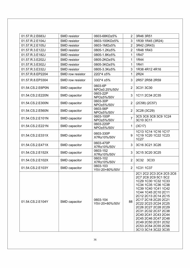
Part 5 Part list of LT-61515E Bom No Part No Part Name QTY
LTD06M-3912C01 02.11.LTD06M3912C01 Main board 1
Part No Name Specification QTY LOCA No
01.57.R.2.E000J SMD resistor 0603-0Ω ±5% 8 2R7 2R31 2R30 2R36 2R38 2R52 3R15 1L22
01.57.R.2.E200F SMD resistor 0603-20Ω 1% 4 1R30 1R32 1R34 1R36
01.57.R.2.E200J SMD resistor 0603-20Ω±5% 121R1 1R2 1R3 1R12 1R14 1R15 2R25 2R26 2R27 2R32 2R33 3R16
01.57.R.2.E470J SMD resistor 0603-47Ω±5% 1 3R19
01.57.R.2.E750F SMD resistor 0603-75Ω±1% 19
1R4 1R5 1R6 1R31 1R33 1R35 1R37 1R13 1R16 1R17 1R18 1R19 1R20 3R17 3R44 1C26 2R49 2R50 2R51
01.57.R.2.E101J SMD resistor 0603-100Ω±5% 19
2R1 2R4 1R51 2R15 2R17 2R39 2R41 2R42 2R46 2R47 3R13 3R14 2R8 3R11 3R12 3R29 3R30 3R48 3R52
01.57.R.2.E221J SMD resistor 0603-220Ω±5% 1 3R27 01.57.R.2.E301J SMD resistor 0603-300Ω±5% 1 3R25 01.57.R.2.E471J SMD resistor 0603-470Ω±5% 3 3R18 3R26 3R36 01.57.R.2.E681J SMD resistor 0603-680Ω±5% 4 3R47 3R50 4R1 (2R55)
01.57.R.2.E102J SMD resistor 0603-1KΩ±5% 10 4R3 4R4 4R7 4R8 3R20 3R22 3R23 3R34 3R39 4R5
01.57.R.2.E222J SMD resistor 0603-2.2KΩ±5% 1 2R43
01.57.R.2.E272J SMD resistor 0603-2.7KΩ±5% 8 2R9 1R21 1R22 1R23 1R24 2R10 2R53 2R54
01.57.R.2.E332J SMD resistor 0603-3.3KΩ±5% 1 2R40
01.57.R.2.E472J SMD resistor 0603-4.7KΩ±5% 8 2R2 2R5 2R14 3R35 3R38 4R9 4R10 4R11
01.57.R.2.E103J SMD resistor 0603-10KΩ±5% 47
2R3 2R6 3R5 3R6 3R7 3R8 3R9 4R2 4R6 1R10 1R11 1R40 1R46 1R49 1R53 2R11 2R12 2R16 2R18 2R19 2R20 2R21 2R22 2R23 2R44 2R45 3R10 3R31 3R33 3R37 3R41 1R55 3R28 3R53 3R54 3R55 3R56 3R1 3R2 3R3 3R4 3R57 3R58 3R59 3R60 3R60 3R62
01.57.R.2.E273J SMD resistor 0603-27KΩ±5% 1 3R21 01.57.R.2.E303J SMD resistor 0603-30KΩ±5% 1 3R40 01.57.R.2.E393J SMD resistor 0603-39KΩ±5% 2 3R45 3R49 01.57.R.2.E473J SMD resistor 0603-47KΩ±5% 4 1R25 1R26 1R27 1R28
36
01.57.R.2.E683J SMD resistor 0603-68KΩ±5% 2 3R46 3R51 01.57.R.2.E104J SMD resistor 0603-100KΩ±5% 3 1R39 1R45 (3R24) 01.57.R.2.E105J SMD resistor 0603-1MΩ±5% 2 3R42 (3R43) 01.57.R.3.E122J SMD resistor 0805-1.2K±5% 2 1R48 1R43 01.57.R.3.E182J SMD resistor 0805-1.8K±5% 1 1R47 01.57.R.3.E202J SMD resistor 0805-2KΩ±5% 1 1R44 01.57.R.3.E302J SMD resistor 0805-3KΩ±5% 1 1R41 01.57.R.3.E332J SMD resistor 0805-3.3K±5% 3 1R38 4R12 4R16 01.57.R.8.EP2204 SMD row resistor 22Ω*4 ±5% 1 2R24
01.57.R.8.EP3304 SMD row resistor 33Ω*4 ±5% 3 2R57 2R58 2R59
01.54.CS.2.E6P0N SMD capacitor 0603-6P NPO±0.25%/50V 2 3C31 3C30
01.54.CS.2.E220N SMD capacitor 0603-22P NPO±5%/50V 3 1C11 2C34 2C35
01.54.CS.2.E300N SMD capacitor 0603-30P NPO±5%/50V 2 (2C58) (2C57)
01.54.CS.2.E560N SMD capacitor 0603-56P NPO±5%/50V 2 3C28 (3C29)
01.54.CS.2.E101N SMD capacitor 0603-100P NPO±5%/50V 7 3C5 3C6 3C8 3C9 1C24
3C10 3C11
01.54.CS.2.E221N SMD capacitor 0603-220P NPO±5%/50V 1 (3C17)
01.54.CS.2.E331X SMD capacitor 0603-330P X7R±10%/50V 9
1C13 1C14 1C16 1C17 1C19 1C20 1C22 1C23 1C27
01.54.CS.2.E471X SMD capacitor 0603-470P X7R±10%/50V 3 3C16 3C21 3C26
01.54.CS.2.E152X SMD capacitor 0603-152 X7R±10%/50V 3 3C15 3C20 3C25
01.54.CS.2.E102X SMD capacitor 0603-102 X7R±10%/50V 2 3C32 3C33
01.54.CS.2.E103Y SMD capacitor 0603-103 Y5V-20+80%/50V 2 1C31 1C37
01.54.CS.2.E104Y SMD capacitor 0603-104 Y5V-20+80%/50V 88
2C1 2C2 2C3 2C4 2C5 2C6 2C7 2C8 2C9 5C1 5C2 1C29 1C30 1C32 1C33 1C34 1C35 1C36 1C38 1C39 1C40 1C41 1C42 1C44 1C45 2C10 2C11 2C12 2C13 2C14 2C15 2C17 2C18 2C20 2C21 2C22 2C23 2C24 2C25 2C26 2C27 2C28 2C29 2C31 2C32 2C37 2C38 2C40 2C41 2C43 2C44 2C45 2C46 2C47 2C48 2C49 2C50 2C51 2C52 2C53 2C54 2C55 2C56 3C13 3C14 3C22 3C35

37
3C39 3C40 1C1 3C1 3C3 3C4 3C23 3C24 3C27 3C34 1C28 1C46 1C47 1C48 3C42 3C44 1C49 1C50 1C51 1C52 1C60
01.54.CS.2.E104X SMD capacitor 0603-104 X7R±10%/50V 16
1C8 1C9 1C10 1C2 1C3 1C4 3C19 2C16 2C19 2C30 2C39 2C42 1C12 1C15 1C18 1C21
01.54.CS.2.E224Y SMD capacitor 0603-224 Y5V-20+80%/16V 5 3C38 3C37 3C41 3C43
3C18
01.34.CL.D.E1U16VC electrolyse capacitor CD110-1UF/16V 5*11 2 3EC33 3EC34
01.34.CL.D.E2U216VC electrolyse capacitor CD110-2.2UF/16V 5*11 4 1EC2 1EC3 1EC4 1EC5
01.34.CL.D.E10U16VC electrolyse capacitor CD110-10UF/16V 5*11 16
3EC5 3EC6 3EC9 3EC10 3EC12 3EC14 3EC15 3EC16 3EC17 3EC18 3EC24 3EC25 3EC26 2EC19 3EC29 3EC30
01.34.CL.D.E22U25V0C electrolyse capacitor CD110-22UF/25V 5*11 1 3EC32
01.34.CL.D.E47U16VC electrolyse capacitor CD110-47UF/16V 5*11 12
2EC1 2EC2 2EC3 2EC4 2EC6 2EC8 2EC10 2EC11 2EC12 2EC16 2EC18 2EC20
01.34.CL.D.E100U16VC electrolyse capacitor CD110-100UF/16V 5*11 22
1EC1 1EC9 1EC11 1EC12 1EC14 1EC15 1EC16 1EC18 3EC19 3EC20 3EC23 2EC5 2EC7 2EC9 2EC15 2EC17 3EC1 3EC4 3EC21 3EC22 3EC27 3EC28
01.34.CL.D.E220U16VD electrolyse capacitor CD110-220UF/16V 6.3*12 4 1EC6 1EC8 1EC13 2EC13
01.34.CL.D.E100U25VD electrolyse capacitor CD110-100UF/25V 6.3*12 6 1EC7 1EC10 3EC3 4EC1
3EC36 1EC19
01.34.CL.D.E470U25VE electrolyse capacitor CD110-470UF/25V 8*14 5 3C36 3EC37 3EC38 3EC39
3EC31
01.13.L.Z.ESB50 SMD magnetism bead 0805-50Ω 9 1FB1 1FB2 3FB1 3FB2
3FB3 1L2 1L4 1L5 1L19
01.13.L.Z.ESB50P SMD magnetism bead 0805-50Ω PB 14
1L10 1L13 2L1 2L2 2L3 2L4 2L5 2L6 2L7 2L8 2L9 2L10 2L11 2L12
01.13.L.Z.ESA50 SMD magnetism bead 0603-50Ω 1 1L1
01.13.L.Z.ESC50 SMD magnetism bead 1206-50Ω 4 1L14 2L14 2L15 2L16
01.13.L.Z.ED50A DIP magnetism bead 50Ω(3.5*6.0*0.8) 3 3L1 3L2 3L5
01.13.L.L.S.E002 SMD inductor 0603-10UH 3 1L16 1L17 1L18

38
01.13.L.L.S.E010 SMD inductor 0805-2.7UH 4 1L6 1L7 1L8 1L9
01.13.L.L.S.E085 SMD jar install inductor
SLF12575T-470M2R7 2 1L11 1L20
01.13.L.L.D.E150 DIP inductor LH0608-33UH 1 1L12 01.13.L.L.D.E038 Color code inductor 33UH DIP 2 3L4 3L3 01.41.D.WS.E5V1 SMD zener diode 5.1V 2 3D8 2D1 01.41.D.PS.ELL4148 Diode LL4148 SMD 3 3D1 3D2 3D3 01.41.D.PS.EBAV99 Diode BAV99LT1 SMD 1 5D1
01.42.Q.S.E2N3904 Audion 2N3904 SMD 161Q1 1Q3 1Q5 1Q6 2Q1 2Q2 2Q4 3Q1 3Q2 3Q3 3Q4 3Q5 3Q6 3Q7 4Q2 4Q4
01.42.Q.S.E2N3906 Audion 2N3906 SMD 5 Q1 4Q1 4Q3 1Q2 1Q4 01.41.D.PS.ESS24 Diode SS24 SMD 1 1D2 01.41.D.PS.ESK34 Diode SK34 SMD 1 1D1
01.00.JZ.E18432A DIP oscillator 18.432MHZ-49S-12P 1 3Y1
01.00.JZ.E196608A DIP oscillator 19.6608MHZ-49S-20P 1 2Y1
01.44.IC.S.EV330 IC FSAV330 SMD 1 1U1
01.44.IC.S.E3415 IC MSP3415G SMD 1 3U2 01.44.IC.S.EAP1510 IC AP1510 SMD 1 1U2 01.44.IC.S.E1513S IC AP1513S SMD 1 1U3
01.44.IC.S.EA11171V8 IC AZ1117H-1.8 SMD 1 1U4
01.44.IC.S.ES9435 IC FDS9435 SMD 2 1U5 1U7
01.44.IC.S.E24C32 IC AT24C32AN SMD 1 2U2
01.44.IC.S.E8125 IC FLI8125-LF SMD 1 2U3
01.44.IC.D.EL7808 IC L7808C-V DIP 1 8U1
01.44.IC.D.ETDA1517P IC TDA1517P DIP 1 3U3
01.46.IC.EAT49BV IC AT49BV040B SMD 1 2U1
01.44.IC.S.E4052 IC CD4052 SMD 1 3U1 01.44.IC.S.EPESD5V0L5 IC PESD5V0L5
SMD 4 5U1 5U2 5U3 5U4
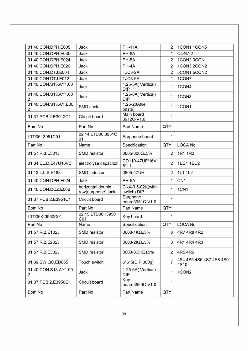
01.31.GPT.E063 Tuner MPE05-1-E DIP 1 TUNER1 01.40.CON.DCZ.E001 Jack DASW-8 DIP 1 1CN1 01.40.CON.DCZ.E331 SCART Jack CS112 DIP 1 1CON6 01.40.CON.DCZ.E347 Same core Jack AV5-8.4-13/PB-27 1 1CN2 01.40.CON.DCZ.E167 Same core Jack AV2-8.4-13/PB 1 1CN3
01.40.CON.DCZ.E018 Power jack DDK2.5 DIP 1 1JP1
39
01.40.CON.DPH.E005 Jack PH-11A 2 1CON1 1CON5 01.40.CON.DPH.E035 Jack PH-8A 1 CON7-2 01.40.CON.DPH.E024 Jack PH-5A 2 1CON2 3CON1 01.40.CON.DPH.E020 Jack PH-4A 2 1CON3 2CON2 01.40.CON.DTJ.E004 Jack TJC3-2A 2 5CON1 5CON2 01.40.CON.DTJ.E012 Jack TJC3-6A 1 1CON7 01.40.CON.S13.AY1.001 Jack 1.25-5A( Vertical)
DIP 1 1CON4
01.40.CON.S13.AY1.002 Jack 1.25-6A( Vertical)
DIP 1 1CON8
01.40.CON.S13.AY.E002 SMD Jack 1.25-20A(lie
paste) 1 2CON1
01.37.PCB.2.E3912C1 Circuit board Main board 3912C-V1.0 1
Bom No Part No Part Name QTY
LTD06I-3951C01 02.14.LTD06I3951C01 Earphone board 1
Part No Name Specification QTY LOCA No
01.57.R.3.E301J SMD resistor 0805-300Ω±5% 2 1R1 1R2
01.34.CL.D.E47U16VC electrolyse capacitor CD110-47UF/16V 5*11 2 1EC1 1EC2
01.13.L.L.S.E188 SMD inductor 0805-47UH 2 1L1 1L2
01.40.CON.DPH.E024 Jack PH-5A 1 CN1
01.40.CON.DCZ.E066 horizontal double row(earphone) jack
CKX-3.5-02K(with switch) DIP 1 1CN1
01.37.PCB.2.E3951C1 Circuit board Earphone board3951C-V1.0 1
Bom No Part No Part Name QTY
LTD06K-3950C01 02.15.LTD06K3950C01 Key board 1
Part No Name Specification QTY LOCA No
01.57.R.2.E102J SMD resistor 0603-1KΩ±5% 3 4R7 4R8 4R2
01.57.R.2.E202J SMD resistor 0603-2KΩ±5% 3 4R1 4R4 4R3
01.57.R.2.E332J SMD resistor 0603-3.3KΩ±5% 2 4R5 4R6
01.39.SW.QC.ED665 Touch switch 6*6*5(DIP 300g) 7 4S4 4S5 4S6 4S7 4S8 4S9 4S10
01.40.CON.S13.AY1.002 Jack 1.25-6A( Vertical)
DIP 1 1CON2
01.37.PCB.2.E3950C1 Circuit board Key board3950C-V1.0 1
Bom No Part No Part Name QTY
40
LTD06I-3915C01 02.14.LTD06I3915C01
VGA interface board 1
Part No Name Specification QTY LOCA No 01.57.R.2.E000J SMD resistor 0603-0Ω ±5% 6 1R1 1R2 1R3 1C1 1C2 1C301.57.R.2.E101J SMD resistor 0603-100Ω±5% 6 1R4 1R5 5R1 5R2 5R3 5R401.57.R.2.E222J SMD resistor 0603-2.2KΩ±5% 2 5R8 5R9 01.57.R.2.E272J SMD resistor 0603-2.7KΩ±5% 4 1R6 1R7 5R10 5R11 01.57.R.2.E473J SMD resistor 0603-47KΩ±5% 2 1R8 1R9
01.57.R.3.E000J SMD resistor 0805-0Ω ±5% 5 5L1 5L2 5L3 5L4 5L5
01.54.CS.2.E104Y SMD capacitor 0603-104 Y5V-20+80%/50V 3 1C4 5C5 5C6
01.34.CL.D.E2U216VC electrolyse capacitor CD110-2.2UF/16V 5*11 2 1EC1 1EC2
01.34.CL.D.E100U16VC electrolyse capacitor CD110-100UF/16V 5*11 1 1EC3
01.41.D.PS.ELL4148 Diode LL4148 SMD 2 5D2 5D1
01.40.CON.DPH.E005 Jack PH-11A 1 1CON1
01.40.CON.DPH.E020 Jack PH-4A 1 1CON2
01.40.CON.DCZ.E007 VGAJack EV-015FC/15 pin DIP 1 5CON1
01.40.CON.DCZ.E102 Perch earphpne jack CKX-3.5-02(without switch) DIP 1 5CON2
01.46.IC.E24C02 IC 24C02 SMD 1 5U2 01.44.IC.S.EPESD5V0L5 IC PESD5V0L5
SMD 2 5U1 5U3
01.37.PCB.2.E3915C2 Circuit board VGA interface board3915C-V2.0 1
Bom No Part No Part Name QTY
LTD06P-2956C01 02.19.LTD06P2956C01 Power board 1
Part No Name Specification QTY LOCA No 01.57.R.3.E681J SMD resistor 0805-680Ω±5% 1 R9 01.57.R.3.E472J SMD resistor 0805-4.7KΩ±5% 1 R13 01.57.R.3.E222J SMD resistor 0805-2.2KΩ±5% 1 R12 01.57.R.3.E123J SMD resistor 0805-12KΩ±5% 2 R3 R11 01.57.R.4.E4R7J SMD resistor 1206-4.7Ω±5% 1 R6 01.57.R.4.E390J SMD resistor 1206-39Ω±5% 2 R7 R8 01.57.R.4.E222J SMD resistor 1206-2.2KΩ±5% 1 R10 01.57.R.4.E514J SMD resistor 1206-510KΩ±5% 2 R1 R2 01.57.R.4.E392J SMD resistor 1206-3.9KΩ±5% 1 R15
01.57.R.C.EC105 Carbon film resistor RT1/6W-1MΩ 1 R4
01.57.R.C.EG563 Carbon film resistor RT2W-56KΩ 1 R5

41
01.57.R.R.E5D11 Hot agile resistor NTC-5D-11 1 TH1
01.57.R.Y.E10K Press agile resistor 10K.471 1 VR1
01.54.CS.3.E104X SMD capacitor 0805-104 X7R±10%/50V 2 C13 C10
01.54.CS.3.E473X SMD capacitor 0805-473 X7R±10%/50V 1 C5
01.54.CS.4.E102X200V SMD capacitor 1206-102 X7R±10%/200V 1 C6
01.34.CL.D.E150U400V electrolyse capacitor150uF/400V 18*36 ±20% 105 Low ESR
1 C1
01.34.CL.D.E1000U25V electrolyse capacitor1000uF/25V 10*20 ±20% 105 Low ESR
2 C7 C8
01.34.CL.D.E470U25V electrolyse capacitor470uF/25V 8*20 ±20% 105 Low ESR
1 C9
01.00.CD.CP.E1031KV Ceramic capacitor 103/1KV 1 C2
01.00.CD.CP.E2221KVA Ceramic capacitor 222/1KV 1 C3
01.00.CD.GY.E104275V Hi-voltage capacitor 104/275V X2 1 CX2
01.00.CD.GY.E224275V Hi-voltage capacitor 224/275V X2 1 CX1
01.00.CD.GY.E471400V Hi-voltage capacitor 471/400V Y1 2 CY1 CY2
01.00.CD.GY.E222400V Hi-voltage capacitor 222/400V Y1 1 CY3
01.34.CL.D.E22U35VB electrolyse capacitor CD11X-22UF/35V 5*7(105 ) 1 C4
01.13.L.L.D.E155 Filter LCL-401 1 Lc1
01.13.L.L.D.E180 Filter LCL-203B DIP 1 Lc2
01.13.L.L.D.E181 Inductor L620-3uH DIP 1 L1
01.13.L.Z.ED50B DIP magnetism bead 50Ω(3.5*4.7*0.8) 1 L2
01.41.D.PD.E1U08 Diode 1U08 DIP 1 D1
01.41.D.PD.EFR107 Diode FR107 DIP 1 D1
01.41.D.PD.EFR104 Diode FR104 DIP 1 D2
01.41.D.PD.ESF20NC15 Diode SF20NC15M
DIP 2 D3 D4
01.41.D.PD.E2015CT Diode MBRF20150CT DIP 2 D3 D4
42
01.41.D.WD.E10V DIP zenzer diode 10V 1 ZD1
01.41.D.WD.E20V DIP zenzer diode 20V 1 ZD2
01.44.IC.D.EM0765 IC FSCM0765RGWDTU DIP 1 U5
01.44.IC.D.EPC817 IC PC817 DIP 1 U2
01.44.IC.D.EKA431A IC KA431AZ DIP 1 U3
01.41.D.PD.EUS4K80 Diode US4K 80R DIP 1 BD1
01.41.D.PD.EGBU406 Diode GBU406 DIP 1 BD1
01.41.D.PD.EGBU408 Diode GBU408 DIP 1 BD1
01.41.D.PD.EPQ322001 Transformer BCK-PQ3220-01 DIP 1 TR1
01.40.CON.DCZ.E129 Connector VH 1 CN1
01.40.CON.DTJ.E008 Jack TJC3-4A 1 CN3
01.40.CON.DTJ.E012 Jack TJC3-6A 1 CN4
01.38.FUSE.D.E3K315 Fuse 3K 3.15A 250V DIP 1 F1
01.38.FUSE.D.E32S315 Fuse 32S 3.15A 250V DIP 1 F1
01.38.FUSE.D.E315A250V Fuse ICP 3.15A250V 1 F1
01.00.FZ.ZZ.E010 J line 15mm 2 J1 J5
01.00.FZ.ZZ.E003 J line 10mm 2 J2 J3
01.00.FZ.ZZ.E007 J line 12.5mm 1 J4
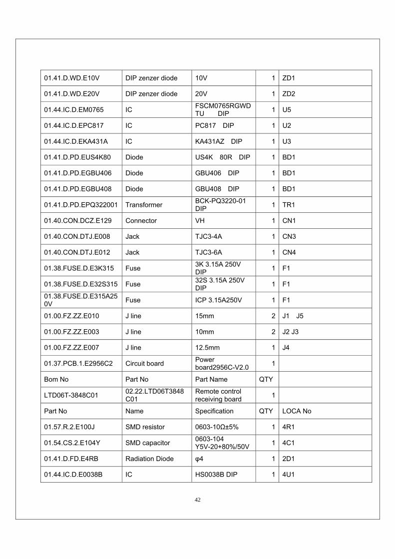
01.37.PCB.1.E2956C2 Circuit board Power board2956C-V2.0 1
Bom No Part No Part Name QTY
LTD06T-3848C01 02.22.LTD06T3848C01
Remote control receiving board 1
Part No Name Specification QTY LOCA No
01.57.R.2.E100J SMD resistor 0603-10Ω±5% 1 4R1
01.54.CS.2.E104Y SMD capacitor 0603-104 Y5V-20+80%/50V 1 4C1
01.41.D.FD.E4RB Radiation Diode φ4 1 2D1
01.44.IC.D.E0038B IC HS0038B DIP 1 4U1

43
01.40.CON.S13.AY1.001 Jack 1.25-5A( Vertical)
DIP 1 1CON1
01.37.PCB.2.E3848C3 Circuit board Remote control receiving board3848C-V3.0
1
Bom No Part No Part Name QTY
MINV15-07SVA1B02 02.07.MINV1507SVA1B02 Inverter 1
Part No Name Specification QTY LOCA No
01.57.R.4.E471J SMD resistor 1206-470Ω±5% 1 R2
01.57.R.2.E152J SMD resistor 0603-1.5KΩ±5% 1 R1
01.57.R.2.E561F SMD resistor 0603-560Ω±1% 2 R6 R14
01.57.R.2.E681J SMD resistor 0603-680Ω±5% 2 R4 R10
01.57.R.2.E202J SMD resistor 0603-2KΩ±5% 1 R3
01.57.R.2.E103J SMD resistor 0603-10KΩ±5% 2 R19 R8
01.57.R.2.E153J SMD resistor 0603-15KΩ±5% 2 R13 R16
01.57.R.2.E203J SMD resistor 0603-20KΩ±5% 1 R18
01.57.R.2.E223J SMD resistor 0603-22KΩ±5% 2 R5 R11
01.57.R.2.E683J SMD resistor 0603-68KΩ±5% 2 R7 R15
01.57.R.2.E104J SMD resistor 0603-100KΩ±5% 1 R9
01.57.R.2.E474J SMD resistor 0603-470KΩ±5% 1 R17
01.54.CS.2.E101N SMD capacitor 0603-100P NPO±5%/50V 1 C8
01.54.CS.2.E821N SMD capacitor 0603-820P NPO±5%/50V 1 C14
01.54.CS.2.E222X SMD capacitor 0603-222 X7R±10%/50V 3 C11 C17 C18
01.54.CS.2.E472X SMD capacitor 0603-472 X7R±10%/50V 2 C12 C4
01.54.CS.2.E102X SMD capacitor 0603-102 X7R±10%/50V 2 C5 C13
01.54.CS.2.E223X SMD capacitor 0603-223 X7R±10%/50V 1 C7
01.54.CS.2.E104X SMD capacitor 0603-104 X7R±10%/50V 1 C16
01.54.CS.2.E474Y SMD capacitor 0603-474 Y5V+80-20%/50V 1 C19

44
01.54.CS.2.E105Y16V SMD capacitor 0603-105 Y5V-20+80%/16V 4 C6 C15 C22 C23
01.54.CS.2.E225Y SMD capacitor 0603-225 Y5V-20+80%/10V 1 C24
01.35.CC.E121010U25VX
SMD ceramic capacitor
C3225X5R1E106KT 2 C10 C3
01.54.CS.6.E100 SMD capacitor 1808-10P/3KV NPO±5% 2 C2 C9
01.34.CL.D.EKW220U25VO electrolyse capacitor KW-220UF/25V
8*9 2 C1 C21
01.41.D.WS.EUDZ7V5B Diode UDZ7V5B(7.5V) 1 D1
01.41.D.PS.E1SS355 Diode 1SS355 SMD 3 D2 D3 D4
01.41.D.PS.EBAV99 Diode BAV99LT1 SMD 4 CR1 CR2 CR3 CR4
01.42.Q.S.E2N3904 Audion 2N3904 SMD 2 Q3 Q1
01.42.Q.S.E2N3906 Audion 2N3906 SMD 1 Q4
01.42.Q.S.E2N7002 Transistor 2N7002 SMD 1 Q5
01.44.IC.S.EAP4511GM Transistor AP4511GM SMD 2 Q2 Q6
01.13.L.R.E114 Transformer NIA19LES021 2 T1 T2
01.00.YS.TZ.T.E747 Transformer label Label001 2 label
01.38.FUSE.S.EF1206HI3000 Fuse F1206HI-3000
SMD 1 F1
01.38.FUSE.S.E66002 Fuse 0466002.NR 1 F1
01.44.IC.S.E3193 IC Bit3193 SMD 1 U1
01.40.CON.DPH.E058 Jack PH-5A 1 CN1
01.40.CON.S80.E001 SMD hi-voltage Jack BHR-2VS 2 CN2 CN3
01.37.PCB.2.E3719C1 Circuit board Inverter board3719C-V1.0 1

45
Part 6 Debugging Procedures 1. Signal process diagram

46
2. Debugging Strategy
A
IR and Keys are All Ok?
Check communications betweenIR,Key mode and FLI8125
Check periphery circuitOf IR,Keypad,drive IC
Check wiring circuit ofIR,KeypadEnd debugging
NO
47
3. Tips Of Some Typical Troubleshooting
White screen First check voltage in HI-voltage Board; otherwise check the voltage of MAIN board , if abnormal , the problem occurs in 1U2. If the voltage is OK, check the LVDS. At last the connection between the main board and drive board may be the target for troubleshooting.
Black screen
This problem often arise from the voltage input to the screen, so the first step is to check the voltage of invert circuit. Otherwise check if the status is standby. If in TV mode, check the power for tuner is correct. No color
Check if the connection with the external device is correct. Otherwise make sure the saturation is not zero. At last the problem may arise from the FLI8125. Abnormal picture
Check if the range of the signal input to FLI8125 is correct. If no, the problem may be in the AFE(Analog Front End). Otherwise make sure the color system is correct. Then check the LVDS and the LCD Screen. Pictures with no sound Firstly, make sure the speakers works well. If so, the trouble mostly occurred in TDA1517 in 3U3 in main board, then MSP3415G in 3U2. Sounds with no picture
Check if any signal inputs to FLI8125, if yes, the problem may be in the AFE. Otherwise check the LVDS.