Embed Size (px)
Citation preview
User’s M
anual
E1 Emulator Additional Document for User’s Manual
(Notes on Connection for RL78)
Supported Devices: RL78 Family RL78/G13 RL78/G14 RL78/I1A
All information contained in these materials, including products and product specifications, represents information on the product at the time of publication and is subject to change by Renesas Electronics Corp. without notice. Please review the latest information published by Renesas Electronics Corp. through various means, including the Renesas Electronics Corp. website (http://www.renesas.com).
www.renesas.com Rev.1.00 July 2011

Contents
R20UT0763EJ0100 Rev.1.00 Page 3 of 22 July 15, 2011
Contents
1. Outline.................................................................................................................................................................................................. 4
1.1 Features................................................................................................................................................................................................................. 4 1.2 Configuration of Manuals .................................................................................................................................................................................... 4
2. Designing the User System ................................................................................................................................................................. 5
2.1 Connecting the Emulator with the User System.................................................................................................................................................. 5 2.2 Pin Assignments of the Connector on the User System ...................................................................................................................................... 6 2.3 Recommend Circuit between the Connector and the MCU ................................................................................................................................ 7 2.3.1 Recommend Circuit Connection ..............................................................................................................................................................7 2.3.2 Regarding Connection of RESET ............................................................................................................................................................8
3. Setting of Security ID and Securing of debugging resources ............................................................................................................ 11
3.1 Setting of Security ID......................................................................................................................................................................................... 11 3.2 Setting of On-chip debug option byte ................................................................................................................................................................ 13 3.3 Securing of area for debugging .......................................................................................................................................................................... 14
4. Specifications..................................................................................................................................................................................... 17
5. Notes on Usage ................................................................................................................................................................................. 18
5.1 Lists .................................................................................................................................................................................................................... 18 5.2 Details................................................................................................................................................................................................................. 19
Outline
1. Outline
1.1 Features E1 Emulator is an on-chip debug emulator with flash programming function, which is used for debugging and programming a program
to be embedded in on-chip flash memory microcontrollers. This product can debug with the target microcontroller connected to the user
system, and can write programs to the on-chip flash memory of microcontrollers.
1.2 Configuration of Manuals Documentation for the E1/E20 emulator manual is in two parts: the E1/E20 Emulator User’s Manual and the E1/E20 Emulator
Supplementary Document for the User’s Manual (this manual). Different versions of the latter correspond to different sets of MCU. Be
sure to read both of the manuals before using the E1/E20 emulator (hereinafter referred to as "the emulator").
(1) The E1/E20 emulator user’s manual has the following contents:
Components of the emulators
Emulator hardware specification
Connection to the emulator and the host computer and user system
(2) The E1/E20 Emulator Supplementary Document for the User’s Manual has the following contents:
For use in hardware design, an example of connection and the interface circuit required to connect the emulator.
Notes on using the emulator
Software specifications and so on for using each microcomputers
R20UT0763EJ0100 Rev.1.00 Page 4 of 22 July 15, 2011
Designing the User System
2. Designing the User System
To connect the E1 emulator (hereinafter referred to as the emulator), a connector for the user system interface cable must be mounted
on the user system. When designing the user system, read this section of this manual and the hardware manual for the MCUs.
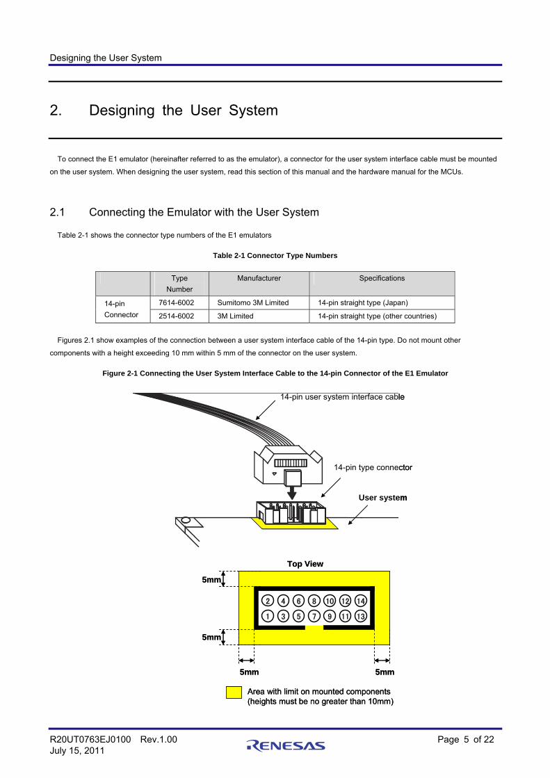
2.1 Connecting the Emulator with the User System
Table 2-1 shows the connector type numbers of the E1 emulators
Table 2-1 Connector Type Numbers
Type
Number
Manufacturer Specifications
7614-6002 Sumitomo 3M Limited 14-pin straight type (Japan) 14-pin
Connector 2514-6002 3M Limited 14-pin straight type (other countries)
Figures 2.1 show examples of the connection between a user system interface cable of the 14-pin type. Do not mount other
components with a height exceeding 10 mm within 5 mm of the connector on the user system.
Figure 2-1 Connecting the User System Interface Cable to the 14-pin Connector of the E1 Emulator
14-pin user system interface cable
14-pin type connector
User system
1 3 5 7 9 11 13
2 4 6 8 10 12 14
5mm
5mm
5mm 5mm
Area with limit on mounted components(heights must be no greater than 10mm)
Top View
14-pin user system interface cable
14-pin type connector
User system
1 3 5 7 9 11 13
2 4 6 8 10 12 14
5mm
5mm
5mm 5mm
Area with limit on mounted components(heights must be no greater than 10mm)
Top View
R20UT0763EJ0100 Rev.1.00 Page 5 of 22 July 15, 2011
Designing the User System
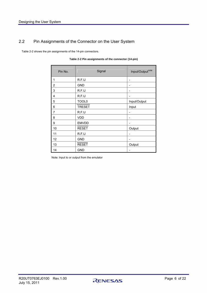
2.2 Pin Assignments of the Connector on the User System
Table 2-2 shows the pin assignments of the 14-pin connectors.
Table 2-2 Pin assignments of the connector (14-pin)
Pin No. Signal Input/Outputnote
1 R.F.U -
2 GND -
3 R.F.U -
4 R.F.U -
5 TOOL0 Input/Output
6 TRESET Input
7 R.F.U -
8 VDD -
9 EMVDD -
10 RESET Output
11 R.F.U -
12 GND -
13 RESET Output
14 GND - Note: Input to or output from the emulator
R20UT0763EJ0100 Rev.1.00 Page 6 of 22 July 15, 2011
Designing the User System
2.3 Recommend Circuit between the Connector and the MCU
2.3.1 Recommend Circuit Connection
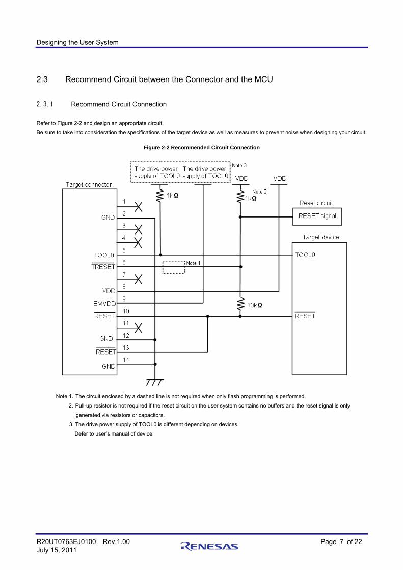
Refer to Figure 2-2 and design an appropriate circuit.
Be sure to take into consideration the specifications of the target device as well as measures to prevent noise when designing your circuit.
Figure 2-2 Recommended Circuit Connection
Note 1. The circuit enclosed by a dashed line is not required when only flash programming is performed.
2. Pull-up resistor is not required if the reset circuit on the user system contains no buffers and the reset signal is only
generated via resistors or capacitors.
3. The drive power supply of TOOL0 is different depending on devices.
Defer to user’s manual of device.
R20UT0763EJ0100 Rev.1.00 Page 7 of 22 July 15, 2011
Designing the User System
2.3.2 Regarding Connection of RESET
This section describes the connection of the reset pin, for which special attention must be paid, in the circuit connection example shown in
the previous section.
During on-chip debugging, a reset signal from the user system is input to the emulator, masked, and then output to the target device.
Therefore, the reset signal connection varies depending on whether the emulator is connected.
For flash programming, the circuit must be designed so that the reset signals of the user system and the emulator do not conflict.
Select one of the following methods and connect the reset signal in the circuit. The details of each method are described on the following
pages.
(1) Automatically switching the reset signal via series resistor (recommended; described in recommended circuit connection in the
previous section)
(2) Manually switching the reset signal with jumper
(3) Resetting the target device by power-on reset (POR) only
R20UT0763EJ0100 Rev.1.00 Page 8 of 22 July 15, 2011
Designing the User System
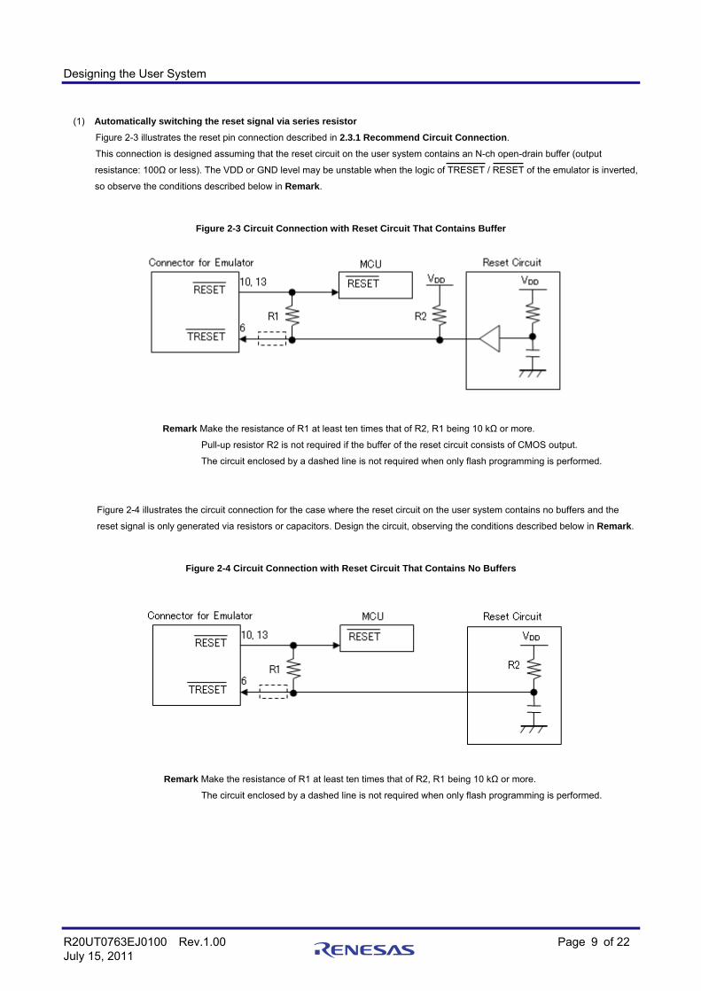
(1) Automatically switching the reset signal via series resistor
Figure 2-3 illustrates the reset pin connection described in 2.3.1 Recommend Circuit Connection.
This connection is designed assuming that the reset circuit on the user system contains an N-ch open-drain buffer (output
resistance: 100Ω or less). The VDD or GND level may be unstable when the logic of TRESET / RESET of the emulator is inverted,
so observe the conditions described below in Remark.
Figure 2-3 Circuit Connection with Reset Circuit That Contains Buffer
Remark Make the resistance of R1 at least ten times that of R2, R1 being 10 kΩ or more.
Pull-up resistor R2 is not required if the buffer of the reset circuit consists of CMOS output.
The circuit enclosed by a dashed line is not required when only flash programming is performed.
Figure 2-4 illustrates the circuit connection for the case where the reset circuit on the user system contains no buffers and the
reset signal is only generated via resistors or capacitors. Design the circuit, observing the conditions described below in Remark.
Figure 2-4 Circuit Connection with Reset Circuit That Contains No Buffers
Remark Make the resistance of R1 at least ten times that of R2, R1 being 10 kΩ or more.
The circuit enclosed by a dashed line is not required when only flash programming is performed.
R20UT0763EJ0100 Rev.1.00 Page 9 of 22 July 15, 2011
Designing the User System
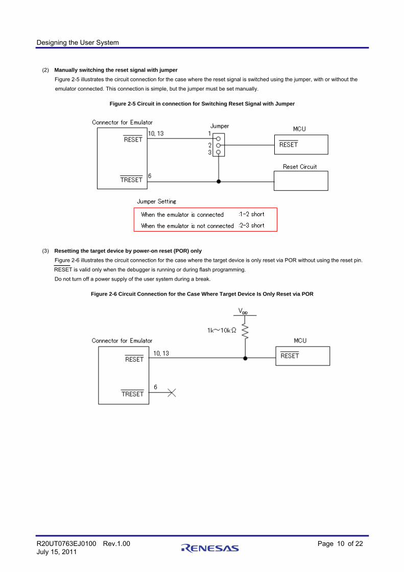
(2) Manually switching the reset signal with jumper
Figure 2-5 illustrates the circuit connection for the case where the reset signal is switched using the jumper, with or without the
emulator connected. This connection is simple, but the jumper must be set manually.
Figure 2-5 Circuit in connection for Switching Reset Signal with Jumper
(3) Resetting the target device by power-on reset (POR) only
Figure 2-6 illustrates the circuit connection for the case where the target device is only reset via POR without using the reset pin.
RESET is valid only when the debugger is running or during flash programming.
Do not turn off a power supply of the user system during a break.
Figure 2-6 Circuit Connection for the Case Where Target Device Is Only Reset via POR
R20UT0763EJ0100 Rev.1.00 Page 10 of 22 July 15, 2011
Setting of Security ID and Securing of debugging resources
3. Setting of Security ID and Securing of debugging resources
The user must prepare the following to perform communication between E1 emulator and the target device and implement each debug
function. Refer to the descriptions on the following sections and set these items in the user program or using the build tool property.
When C-SPY manufactured by IAR Systems is used, read also the following material.
- IAR C-SPY Hardware Debugger Systems User Guide issued by IAR Systems
3.1 Setting of Security ID
This setting is required to prevent the memory from being read by an unauthorized person. Embed a security ID at addresses 0xC4 to
0xCD in the internal flash memory. The debugger starts only when the security ID that is set during debugger startup and the security ID
set at addresses 0xC4 to 0xCD match. If the ID codes do not match, the debugger manipulates the target device in accordance with the
value set to the on-chip debug option byte area (refer to Table 3-2).
If the user has forgotten the security ID to enable debugging, erase the flash memory and set the security ID again.
Caution Do not set all F ("FFFFFFFFFFFFFFFFFFFF") as security ID.
[How to set security ID]
A setting method of the security ID is following. When both (a) and (b) methods are done at a time, method (b) has a priority.
(a) Embed the security ID at addresses 0xC4 to 0xCD in the user program.
(b) Setting of the security ID by build tool common options. (In case of CubeSuite+)
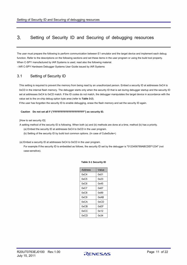
(a) Embed a security ID at addresses 0xC4 to 0xCD in the user program.
For example If the security ID is embedded as follows, the security ID set by the debugger is ″0123456789ABCDEF1234″ (not
case-sensitive).
Table 3-1 Security ID
Address Value
0xC4 0x01
0xC5 0x23
0xC6 0x45
0xC7 0x67
0xC8 0x89
0xC9 0xAB
0xCA 0xCD
0xCB 0xEF
0xCC 0x12
0xCD 0x34
R20UT0763EJ0100 Rev.1.00 Page 11 of 22 July 15, 2011
Setting of Security ID and Securing of debugging resources
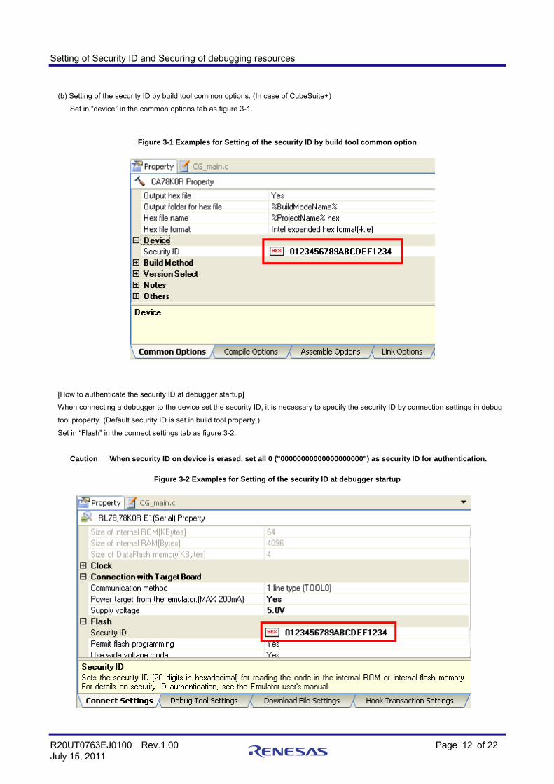
(b) Setting of the security ID by build tool common options. (In case of CubeSuite+)
Set in “device” in the common options tab as figure 3-1.
Figure 3-1 Examples for Setting of the security ID by build tool common option
[How to authenticate the security ID at debugger startup]
When connecting a debugger to the device set the security ID, it is necessary to specify the security ID by connection settings in debug
tool property. (Default security ID is set in build tool property.)
Set in “Flash” in the connect settings tab as figure 3-2.
Caution When security ID on device is erased, set all 0 ("00000000000000000000") as security ID for authentication.
Figure 3-2 Examples for Setting of the security ID at debugger startup
R20UT0763EJ0100 Rev.1.00 Page 12 of 22 July 15, 2011
Setting of Security ID and Securing of debugging resources
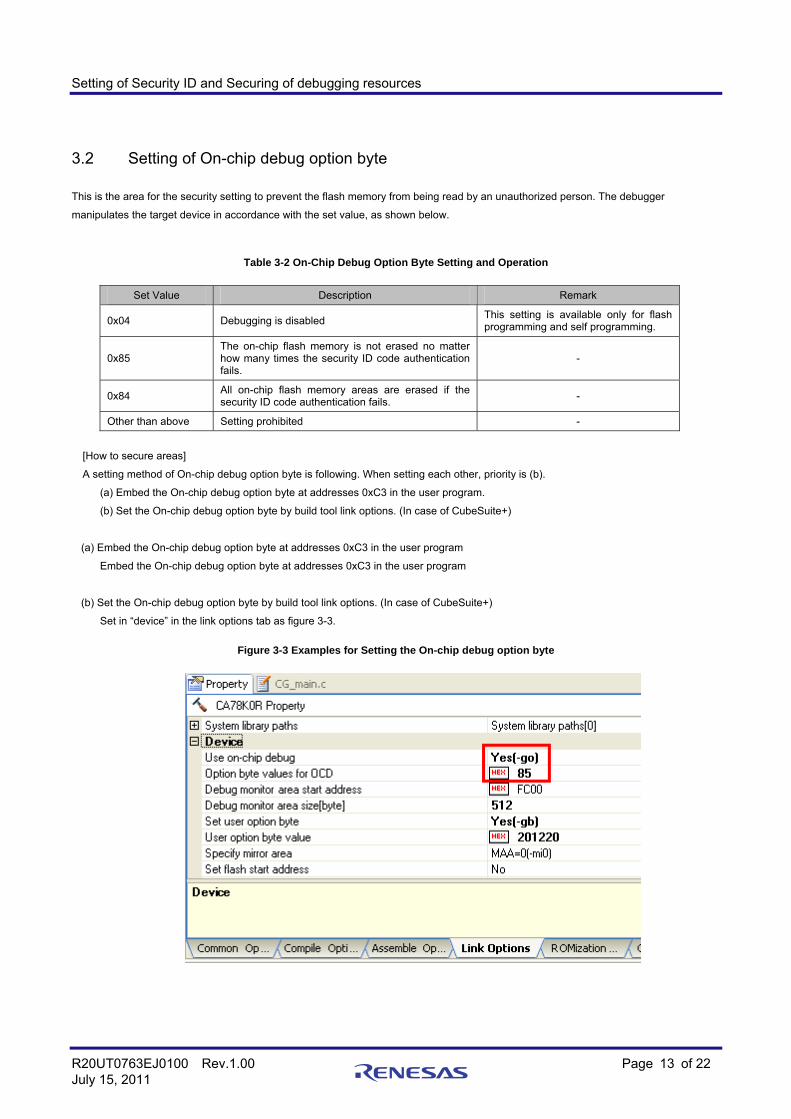
3.2 Setting of On-chip debug option byte
This is the area for the security setting to prevent the flash memory from being read by an unauthorized person. The debugger
manipulates the target device in accordance with the set value, as shown below.
Table 3-2 On-Chip Debug Option Byte Setting and Operation
Set Value Description Remark
0x04 Debugging is disabled This setting is available only for flash programming and self programming.
0x85 The on-chip flash memory is not erased no matter how many times the security ID code authentication fails.
-
0x84 All on-chip flash memory areas are erased if the security ID code authentication fails.
-
Other than above Setting prohibited -
[How to secure areas]
A setting method of On-chip debug option byte is following. When setting each other, priority is (b).
(a) Embed the On-chip debug option byte at addresses 0xC3 in the user program.
(b) Set the On-chip debug option byte by build tool link options. (In case of CubeSuite+)
(a) Embed the On-chip debug option byte at addresses 0xC3 in the user program
Embed the On-chip debug option byte at addresses 0xC3 in the user program
(b) Set the On-chip debug option byte by build tool link options. (In case of CubeSuite+)
Set in “device” in the link options tab as figure 3-3.
Figure 3-3 Examples for Setting the On-chip debug option byte
R20UT0763EJ0100 Rev.1.00 Page 13 of 22 July 15, 2011

Setting of Security ID and Securing of debugging resources
3.3 Securing of area for debugging
The yellow portions in Figure 3-4 are the areas reserved for placing the debug monitor program, so user programs or
data cannot be allocated in these spaces. These spaces must be secured so as not to be used by the user program.
Moreover, this area must not be rewritten by the user program.
Secure the resources for debugging with the contents explained by (a) and (b).
Figure 3-4 Memory Spaces Where Debug Monitor Programs Are Allocated
R20UT0763EJ0100 Rev.1.00 Page 14 of 22 July 15, 2011
Setting of Security ID and Securing of debugging resources
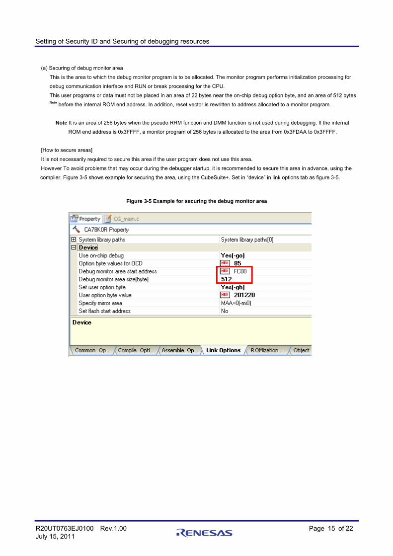
(a) Securing of debug monitor area
This is the area to which the debug monitor program is to be allocated. The monitor program performs initialization processing for
debug communication interface and RUN or break processing for the CPU.
This user programs or data must not be placed in an area of 22 bytes near the on-chip debug option byte, and an area of 512 bytes Note before the internal ROM end address. In addition, reset vector is rewritten to address allocated to a monitor program.
Note It is an area of 256 bytes when the pseudo RRM function and DMM function is not used during debugging. If the internal
ROM end address is 0x3FFFF, a monitor program of 256 bytes is allocated to the area from 0x3FDAA to 0x3FFFF.
[How to secure areas]
It is not necessarily required to secure this area if the user program does not use this area.
However To avoid problems that may occur during the debugger startup, it is recommended to secure this area in advance, using the
compiler. Figure 3-5 shows example for securing the area, using the CubeSuite+. Set in “device” in link options tab as figure 3-5.
Figure 3-5 Example for securing the debug monitor area
R20UT0763EJ0100 Rev.1.00 Page 15 of 22 July 15, 2011
Setting of Security ID and Securing of debugging resources
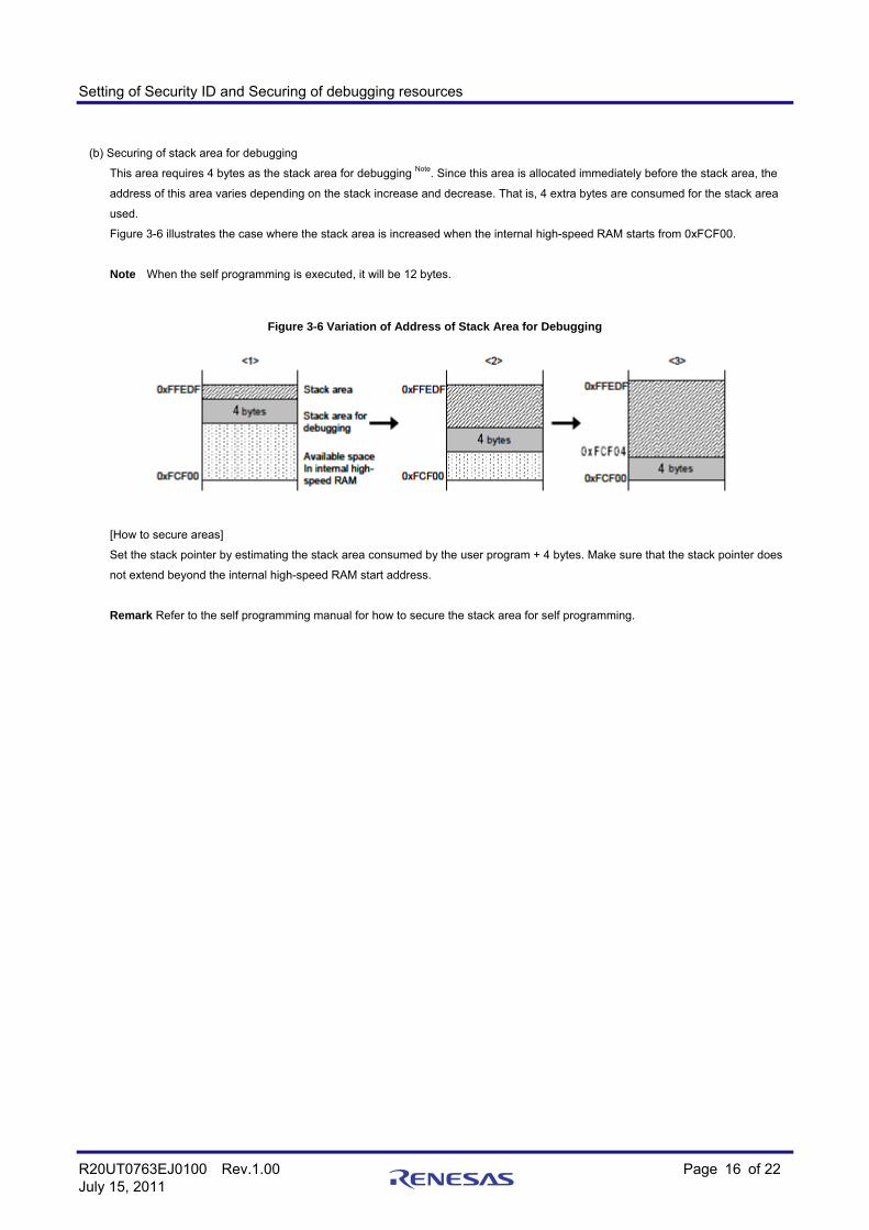
(b) Securing of stack area for debugging
This area requires 4 bytes as the stack area for debugging Note. Since this area is allocated immediately before the stack area, the
address of this area varies depending on the stack increase and decrease. That is, 4 extra bytes are consumed for the stack area
used.
Figure 3-6 illustrates the case where the stack area is increased when the internal high-speed RAM starts from 0xFCF00.
Note When the self programming is executed, it will be 12 bytes.
Figure 3-6 Variation of Address of Stack Area for Debugging
[How to secure areas]
Set the stack pointer by estimating the stack area consumed by the user program + 4 bytes. Make sure that the stack pointer does
not extend beyond the internal high-speed RAM start address.
Remark Refer to the self programming manual for how to secure the stack area for self programming.
R20UT0763EJ0100 Rev.1.00 Page 16 of 22 July 15, 2011
Specifications
4. Specifications
Specifications are below table.
Large Item Middle Item Small Item Specification
Target host machine Computer equipped with a USB port
OS is due to the software tool.
User system interface 14-pin connector
Host machine interface USB2.0 (Full speed/ High speed)
Connection to the user system Connection by the provided user-system interface cable
Power supply function 3.3V or 5.0V, set in software tool, can be supplied to the user system from VDD pin of the emulator (with current up to 200 mA)
Hardware Common
Power supply for the emulator No need (the host computer supplies power through the USB)
Software break 2000 points
Hardware break 1points (commonly used by execution and access)
Break
Forced break Available
Number of events 1points (commonly used by execution and access) Event
Available function Only hardware break
Trace Unavailable
Measurement item From run to break Performance measurement
Performance Resolution 100us, Max. measurement time 100 hour
Real time RAM monitor Available (CPU is used when monitoring)
Direct memory modification Available (CPU is used when executing)
Hot plug-in Unavailable
Related debugging
Security 10-byte ID code authentication
Clock supply Clock mounted on the user system can be used
Security flag setting Available
Related programming
Standalone operation Unavailable (must be connected to host machine)
R20UT0763EJ0100 Rev.1.00 Page 17 of 22 July 15, 2011
Notes on Usage
5. Notes on Usage
Make sure to notes on usage in this section.
5.1 Lists
Table 5-1 Lists of notes on usage
No Item
1 Handling of device that was used for debugging
2 Flash self programming
3 Operation after reset
4 Operation when debugger starts
5 Operation at voltage with which flash memory cannot be written
6 On-chip debug option byte setting (address C3H)
7 Pseudo real-time RAM monitor function
R20UT0763EJ0100 Rev.1.00 Page 18 of 22 July 15, 2011
Notes on Usage
R20UT0763EJ0100 Rev.1.00 Page 19 of 22 July 15, 2011
5.2 Details
No.1 Handling of device that was used for debugging
Do not mount a device that was used for debugging on a mass-produced product, because the flash memory was rewritten during
debugging and the number of rewrites of the flash memory cannot be guaranteed.
Moreover, do not embed the debug monitor program into mass-produced products.
No.2 Flash self programming
If a space where the debug monitor program is allocated is rewritten by flash self programming, the debugger can no longer
operate normally. This caution also applies to boot swapping for such an area.
No.3 Operation after reset
After an external pin reset or internal reset, the monitor program performs debug initialization processing. Consequently, the time
from reset occurrence until user program execution differs from that in the actual device operation. If “No” is selected in the Permit
Flash Programming of the debug tool property, the time until the user program is executed compared with the time when “Yes” is
selected is delayed several 100 ms.
No.4 Operation when debugger starts
When the debugger is started, if there are no the debug monitor program in device for debugging, the internal flash memory is
erased.
No.5 Operation at voltage with which flash memory cannot be written
If any of the following debugger operations <1> to <7>, which involve flash memory rewriting, is performed while flash memory
cannot be rewritten, the debugger automatically changes the register setting so as to enable flash memory rewriting, and restores
the register setting after the operation is completed. If any of the following operations <1> to <7> is performed while flash memory
rewriting has been disabled or operation is performed at a voltage with which flash memory cannot be rewritten, however, the
debugger outputs an error and the operation is ignored.
<1> Writing to internal flash memory
<2> Setting or canceling of software breakpoint
<3> Starting execution at the set software breakpoint position
<4> Step execution at the set software breakpoint position
<5> Step-over execution, Return Out execution
<6> Come Here
<7> If permit is selected in the Flash Programming area in the Configuration dialog box, the following operations cannot be
performed.
a) Setting, changing, or canceling of hardware breaks
b) Masking/unmasking of internal reset
c) Switching of peripheral breaks
No.6 On-chip debug option byte setting (address C3H)
The on-chip debug option byte setting is rewritten arbitrarily by the debugger.
No.7 Pseudo real-time RAM monitor function
Note the following points when using the pseudo real-time RAM monitor function.
<1> Standby mode (HALT or STOP) may be cancelled during monitoring.
<2> The pseudo real-time RAM monitor function does not operate while the CPU operating clock is stopped.
<3> The pseudo real-time RAM monitor function does not operate while the self programming execution.
E1 Emulator Additional Document for User's Manual (Notes on Connection for RL78)
Publication Date: July 15th, 2011 Rev.1.00
Published by: Renesas Electronics Corporation

http://www.renesas.comRefer to "http://www.renesas.com/" for the latest and detailed information.
Renesas Electronics America Inc. 2880 Scott Boulevard Santa Clara, CA 95050-2554, U.S.A.Tel: +1-408-588-6000, Fax: +1-408-588-6130Renesas Electronics Canada Limited1101 Nicholson Road, Newmarket, Ontario L3Y 9C3, CanadaTel: +1-905-898-5441, Fax: +1-905-898-3220Renesas Electronics Europe LimitedDukes Meadow, Millboard Road, Bourne End, Buckinghamshire, SL8 5FH, U.KTel: +44-1628-585-100, Fax: +44-1628-585-900Renesas Electronics Europe GmbHArcadiastrasse 10, 40472 Düsseldorf, Germany Tel: +49-211-65030, Fax: +49-211-6503-1327 Renesas Electronics (China) Co., Ltd.7th Floor, Quantum Plaza, No.27 ZhiChunLu Haidian District, Beijing 100083, P.R.China Tel: +86-10-8235-1155, Fax: +86-10-8235-7679Renesas Electronics (Shanghai) Co., Ltd.Unit 204, 205, AZIA Center, No.1233 Lujiazui Ring Rd., Pudong District, Shanghai 200120, China Tel: +86-21-5877-1818, Fax: +86-21-6887-7858 / -7898 Renesas Electronics Hong Kong LimitedUnit 1601-1613, 16/F., Tower 2, Grand Century Place, 193 Prince Edward Road West, Mongkok, Kowloon, Hong KongTel: +852-2886-9318, Fax: +852 2886-9022/9044Renesas Electronics Taiwan Co., Ltd.13F, No. 363, Fu Shing North Road, Taipei, TaiwanTel: +886-2-8175-9600, Fax: +886 2-8175-9670Renesas Electronics Singapore Pte. Ltd. 1 harbourFront Avenue, #06-10, keppel Bay Tower, Singapore 098632Tel: +65-6213-0200, Fax: +65-6278-8001Renesas Electronics Malaysia Sdn.Bhd. Unit 906, Block B, Menara Amcorp, Amcorp Trade Centre, No. 18, Jln Persiaran Barat, 46050 Petaling Jaya, Selangor Darul Ehsan, MalaysiaTel: +60-3-7955-9390, Fax: +60-3-7955-9510Renesas Electronics Korea Co., Ltd.11F., Samik Lavied' or Bldg., 720-2 Yeoksam-Dong, Kangnam-Ku, Seoul 135-080, KoreaTel: +82-2-558-3737, Fax: +82-2-558-5141
SALES OFFICES
© 2011 Renesas Electronics Corporation. All rights reserved.
Colophon 1.1
E1 EmulatorAdditional Document for User’s Manual
(Notes on Connection for RL78)