Embed Size (px)
Citation preview

8/3/2019 Ee08b097 Akshay Paper
http://slidepdf.com/reader/full/ee08b097-akshay-paper 1/32
Introduction
A fully integrated 2X1 Dual Band DirectConversion Mobile WiMAX tranceiver.
• Features :
–Dual Mode Fractional Divider
– Noise Shaping Transimpedance Amplifier
– 65nm CMOS technology
Presented by
Akshay Bhardwaj
EE08B097
PAPER-PRESENTATION

8/3/2019 Ee08b097 Akshay Paper
http://slidepdf.com/reader/full/ee08b097-akshay-paper 2/32
Outline
Introduction
Transceiver Architecture
Frequency Planning
Circuit DesignMeasurement results
Conclusions

8/3/2019 Ee08b097 Akshay Paper
http://slidepdf.com/reader/full/ee08b097-akshay-paper 3/32
Introduction
WiMAX (Worldwide Interoperability for MicroWave Access) provides
wireless HIGH speed INTERNET service globally.
Mobile WiMAX uses:
• MIMO technique.
• OFDMA modulation scheme.
• High Data rates.
Challenges :• Single chip implementation.
• Low power Consumption
• Floor Planning.
8/3/2019 Ee08b097 Akshay Paper
http://slidepdf.com/reader/full/ee08b097-akshay-paper 4/32
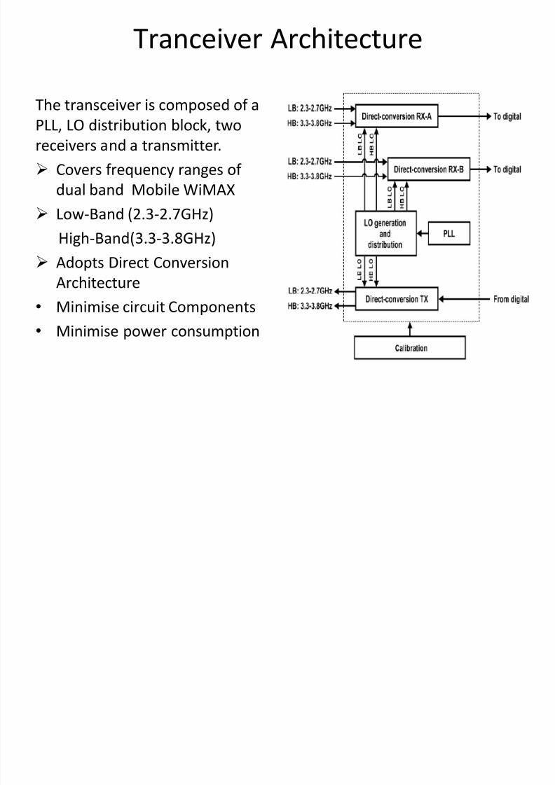
Tranceiver Architecture
The transceiver is composed of a
PLL, LO distribution block, two
receivers and a transmitter.
Covers frequency ranges of
dual band Mobile WiMAX Low-Band (2.3-2.7GHz)
High-Band(3.3-3.8GHz)
Adopts Direct Conversion
Architecture• Minimise circuit Components
• Minimise power consumption

8/3/2019 Ee08b097 Akshay Paper
http://slidepdf.com/reader/full/ee08b097-akshay-paper 5/32
Direct Conversion Receiver Receiver has two RF paths for LOW and HIGH band respectively
RF input first amplified by cascoded common source LNA with LC
tank and down-converted to baseband I/Q signals by I/Q mixers.
The receiver adopts passive mixers to reduce the flicker noise from
switching transistors.
Then, flicker noise from the following TIA op-amp becomesdominant , hence a noise shaping TIA is proposed to improve the
noise figure(NF) of receiver.
In each I/Q path , the down-converted signals are filtered and
amplified by noise shaping TIA, an LPF andd two variable gain
amplifiers.
Finally, signals converted to digital signals by ADCs.

8/3/2019 Ee08b097 Akshay Paper
http://slidepdf.com/reader/full/ee08b097-akshay-paper 6/32
Receiver Block Diagram

8/3/2019 Ee08b097 Akshay Paper
http://slidepdf.com/reader/full/ee08b097-akshay-paper 7/32
Direct Conversion Transmitter The transmitter has two output paths for dual band
operations.Digital I/Q signals are converted to analog baseband
I/Q signals by current steering DACs in I/Q paths.
Next, baseband signals are filtered by reconstructionLPFs and up-converted to RF signal by I/Q mixers.
To reduce circuit components , I/Q mixers are shared
in the LB and HB paths by employing wide-band
passive mixers. The output power of the up-converted RF signal is
controlled by programmable gain stages.

8/3/2019 Ee08b097 Akshay Paper
http://slidepdf.com/reader/full/ee08b097-akshay-paper 8/32
Transmitter Block Diagram

8/3/2019 Ee08b097 Akshay Paper
http://slidepdf.com/reader/full/ee08b097-akshay-paper 9/32
Frequency Planning The single VCO in the PLL is covers frequency tuning range of 8.8-10.8
GHz. The operating frequency of the VCO is divided by 2 and LO signal of 4.4-
5.4Ghz is globally distributed.
LB operation:
For LB ,global LO signal is divided by 2 just before passive mixers in thereceiver and the transmitter.
HB operation:
For HB, global LO signal is divided by 4/3 and then the HB LO signal of
3.3-4.05 G Hz is obtained.
Process : Global LO signal of 4.4-5.4GHz is divided by 2 locally and mixed
with global LO signal to generate LO signal of 6.6-8.1GHz and finally
divided by 2 to generate 3.3-4.05GHz.

8/3/2019 Ee08b097 Akshay Paper
http://slidepdf.com/reader/full/ee08b097-akshay-paper 10/32
Frequency Plan

8/3/2019 Ee08b097 Akshay Paper
http://slidepdf.com/reader/full/ee08b097-akshay-paper 11/32

8/3/2019 Ee08b097 Akshay Paper
http://slidepdf.com/reader/full/ee08b097-akshay-paper 12/32
Circuit Design
Totally three key circuits.
Noise shaping TIA – for mitigating flicker noise
of scaled CCMOS devices
Dual Mode fractional divider – employed in
the inductor less LO distribution path.
Wide-band passive mixer –employed in the
transmitter

8/3/2019 Ee08b097 Akshay Paper
http://slidepdf.com/reader/full/ee08b097-akshay-paper 13/32
A. Noise shaping transimpedance amplifier
In the receiver design , passive mixer topology is adopted toreduce flicker noise , thus reducing the flicker noise from the
TIA becomes very important.
Large Input transistor size of Op-amp can be straightaway
used but it may make Op-amp design much more complex
due to other constraints
- gain, bandwidth, linearity and stability issues.

8/3/2019 Ee08b097 Akshay Paper
http://slidepdf.com/reader/full/ee08b097-akshay-paper 14/32
Basic TIA
Block Diagram :

8/3/2019 Ee08b097 Akshay Paper
http://slidepdf.com/reader/full/ee08b097-akshay-paper 15/32
Noise Shaping TIA
2.

8/3/2019 Ee08b097 Akshay Paper
http://slidepdf.com/reader/full/ee08b097-akshay-paper 16/32
NS-TIA with feedback cap
2.

8/3/2019 Ee08b097 Akshay Paper
http://slidepdf.com/reader/full/ee08b097-akshay-paper 17/32
NS-TIA contd…. I. For basic TIA ,
Signal transfer function(STF) and Noise Transfer Function(NTF) are derived.
• GI =conductance seen from mixer output
• GF = feedback conductance of TIA
• AV = Voltage gain of op-amp
• Vn2 = input referred noise of op-amp

8/3/2019 Ee08b097 Akshay Paper
http://slidepdf.com/reader/full/ee08b097-akshay-paper 18/32
NS-TIA contd…. II ) To suppress flicker noise , we place an additional gain component
before the
op-amp and as input referred noise is suppressed by that gain.
• Ya in the first block is replaced by Yb which is subdivided into Ya and
which is additional gain component.
III ). Since the actual implementation of TIA has 1st
order LPF characteristics ,weconsider
influence of feedback capacitance.
Cf reduces impedance at node X and noise is selectively suppressed only at low
frequencies and NTF is shape into a high pass characteristic.

8/3/2019 Ee08b097 Akshay Paper
http://slidepdf.com/reader/full/ee08b097-akshay-paper 19/32
NS-TIA contd….
• STF and NTF :

8/3/2019 Ee08b097 Akshay Paper
http://slidepdf.com/reader/full/ee08b097-akshay-paper 20/32
NS-TIA contd…. • With the aid of the additional gain boost by , the
STF of the noise-shaping TIA becomes closer tothe ideal low-pass characteristics than the onewithout the gain boost.
• Since the negative conductance cell is placedbetween the virtual ground nodes of the TIA,linearity of the negative conductance cell itself isnot critical.
• Linearity of the proposed TIA is better than aconventional one without the negativeconductance cell because the open loop gain of the TIA is larger

8/3/2019 Ee08b097 Akshay Paper
http://slidepdf.com/reader/full/ee08b097-akshay-paper 21/32
B. Dual-Mode Fractional Divider• It is composed of the divide-by-2 circuit, the gm-cell and the mixer.
• For suppressing the lower side-band spur generated by the mixer in the high-band
operation, we have adopted single side-band (SSB) mixer architecture.

8/3/2019 Ee08b097 Akshay Paper
http://slidepdf.com/reader/full/ee08b097-akshay-paper 22/32
C. Wide-Band Passive Mixer in Transmitter
• Actual implementation is the double-balanced topology for both I/Q
paths.
• The mixer is composed of resistors R1 , a capacitor C1 for AC coupling anda switching transistor M1 . The resistor R1 is the termination resistor as a
load of the mixer, which is also used for biasing the following
programmable gain stage.
• Wideband characteristics are achieved by making small enough to exclude
the effect of parasitic capacitance on impedance at the node X.

8/3/2019 Ee08b097 Akshay Paper
http://slidepdf.com/reader/full/ee08b097-akshay-paper 23/32
Measurement results
By enabling the noise-shaping function, 4 dB
improvement of the receiver output noise at
7 kHz is achieved
Difference of STF is negligibly
small with or without the noise-shaping
function

8/3/2019 Ee08b097 Akshay Paper
http://slidepdf.com/reader/full/ee08b097-akshay-paper 24/32
contd…. • In TIA , by making delta small, we can improve the noise
suppression ratio but we cannot make it too small as when GNbecomes larger than GI + GF , polarity of delta becomes
negative nad the feedback loop becomes unstable.

8/3/2019 Ee08b097 Akshay Paper
http://slidepdf.com/reader/full/ee08b097-akshay-paper 25/32
Layout of the compact dual-mode fractional divider
• The size is 56 um by 118 um
• It is laid out to minimize the lower side-band spur of 1/3*fc
caused by the device mismatches and layout asymmetry of
the single-gate mixers employed in the dual-mode fractional
divider.
• As a result of “fractional-then-distribute” plan all the spurs
become very small.
• All the spur levels are below 60 dBc.

8/3/2019 Ee08b097 Akshay Paper
http://slidepdf.com/reader/full/ee08b097-akshay-paper 26/32
Wide-band spectrum measured at transmitter output.

8/3/2019 Ee08b097 Akshay Paper
http://slidepdf.com/reader/full/ee08b097-akshay-paper 27/32
• Error Vector Magnitudes:
The constellation plots measured at +1 dBm
transmitter output are shown in Figure. Theerror vector magnitudes (EVM) in 2.5 GHz and
3.5 GHz bands are 34.0 dB and 31.0 dB,
respectively

8/3/2019 Ee08b097 Akshay Paper
http://slidepdf.com/reader/full/ee08b097-akshay-paper 28/32
TX constellation plots measured at +1 dBm output.
.

8/3/2019 Ee08b097 Akshay Paper
http://slidepdf.com/reader/full/ee08b097-akshay-paper 29/32
Summary of Transceiver Performance
.

8/3/2019 Ee08b097 Akshay Paper
http://slidepdf.com/reader/full/ee08b097-akshay-paper 30/32
Die micrograph of test chip

8/3/2019 Ee08b097 Akshay Paper
http://slidepdf.com/reader/full/ee08b097-akshay-paper 31/32
Conclusions• A fully integrated 2 RX X 1 TX dual-band direct-conversion mobile WiMAX
transceiver in 65 nm CMOS technology was presented.
• The “distribute-then-fractional” frequency plan is proposed, whichemploys the inductor-less LO distribution with the compact dual-mode
fractional dividers.
• The frequency plan provides higher flexibility for the floor planning of the
long LO distribution path.
• To mitigate the flicker noise of scaled CMOS devices, the noise-shaping TIA
with the negative conductance cell is proposed which keeps signal transfer
function the same and suppresses flicker noise.
• the power consumption of the receiver employing the noise-shaping TIA is
lower than that of the mobile WiMAX transceivers reported previously,
total NF of 3.8 dB and 4.5 dB is achieved in the low-band and the high-band operations , respectively.

8/3/2019 Ee08b097 Akshay Paper
http://slidepdf.com/reader/full/ee08b097-akshay-paper 32/32
THANK YOU

![AKSHAY VENKATESH arXiv:1608.07234v3 …2 AKSHAY VENKATESH algebra”: Hv,S:“ à i Exti (1) SGv pSrGv{Kvs,SrGv{Kvsq Such a construction has been considered by P. Schneider [27] in](https://img.pdfslide.tips/doc/110x75/5ed5d1183e301f01063418a2/akshay-venkatesh-arxiv160807234v3-2-akshay-venkatesh-algebraa-hvsaoe-i.jpg)