Embed Size (px)
Citation preview

EECS130 Integrated Circuit Devices
Professor Ali Javey8/28/2007
Semiconductor FundamentalsLecture 1

Announcements
• Welcome back and happy Fall semester!!!• No discussion sections this week• No HW assignment for this week

Yesterday’s Transistor (1947) Today’s Transistor (2006)
Evolution of Devices

Why “Semiconductors”?• Conductors – e.g Metals• Insulators – e.g. Sand (SiO2 )• Semiconductors
– conductivity between conductors and insulators– Generally crystalline in structure
• In recent years, non-crystalline semiconductors have become commercially very important
Polycrystalline amorphous crystalline

What are semiconductors
Elements: Si, Ge, CBinary: GaAs, InSb, SiC, CdSe, etc.
Ternary+: AlGaAs, InGaAs, etc.

Silicon Crystal Structure
• Unit cell of silicon crystal is cubic.
• Each Si atom has 4 nearest neighbors.
5.43
Electrons and Holes in Semiconductors
Å

Silicon Wafers and Crystal Planes
•
Silicon wafers are usually cut along the (100) plane with a flat or notch to help orient the wafer during IC fabrication.
•
The standard notation for crystal planes is based on the cubic unit cell.
(100) (011) (111)x
y y y
z z z
x x
(100)plane
(011)
flat
Si (111) plane

Bond Model of Electrons and Holes (Intrinsic Si)• Silicon crystal in
a two-dimensionalrepresentation.
Si Si Si
Si Si Si
Si Si Si
Si Si Si
Si Si Si
Si Si Si
Si Si Si
Si Si Si
Si Si Si
• When an electron breaks loose and becomes a conduction electron, a hole is also created.
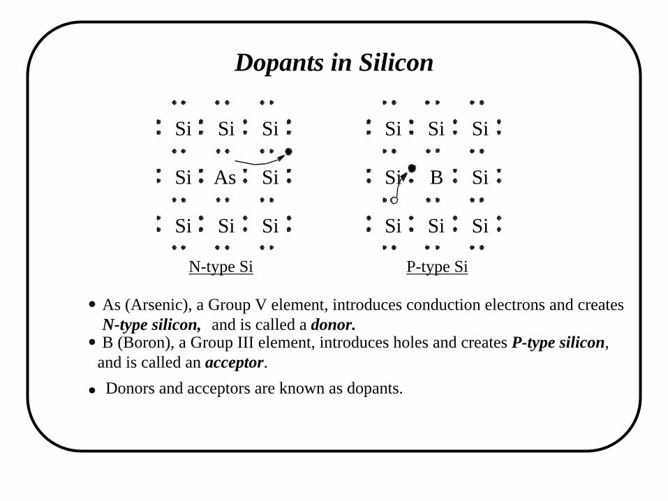
Dopants in Silicon
Si Si Si
Si Si
Si Si Si
Si Si Si
Si Si
Si Si Si
As B
• As (Arsenic), a Group V element, introduces conduction electrons and creates N-type silicon,
• B (Boron), a Group III element, introduces holes and creates P-type silicon, and is called an acceptor.
• Donors and acceptors are known as dopants.
and is called a donor.
N-type Si P-type Si

GaAs, III-V Compound Semiconductors, and Their Dopants
Ga
As
As AsGa
Ga
• GaAs has the same crystal structure as Si.• GaAs, GaP, GaN are III-V compound semiconductors, important for
optoelectronics.• Which group of elements are candidates for donors? acceptors?
GaAs
AsGa Ga

From Atoms to Crystals
• Energy states of Si atom (a) expand into energy bands of Si crystal (b).• The lower bands are filled and higher bands are empty in a semiconductor.• The highest filled band is the valence band.• The lowest empty band is the conduction band .
Decreasing atomic separation
Ener
gy
p
s
isolated atoms lattice spacing
valence band
conduction band

Energy Band Diagram
Conduction band Ec
Ev
Eg Band gap
Valence band
• Energy band diagram shows the bottom edge of conduction band, Ec , and top edge of valence band, Ev .
• Ec and Ev are separated by the band gap energy, Eg .

Measuring the Band Gap Energy by Light Absorption
photons
photon energy: h v > Eg
Ec
Ev
Eg
electron
hole
Bandgap energies of selected semiconductors
• Eg can be determined from the minimum energy (hν) of photons that are absorbed by the semiconductor.
Material PbTe Ge Si GaAs GaP DiamondE g (eV) 0.31 0.67 1.12 1.42 2.25 6.0

Temperature Effect on Band Gap
Decreasing atomic separation
Ener
gy
p
s
isolated atoms lattice spacing
valence band
conduction band
How does the band gap change with temperature?
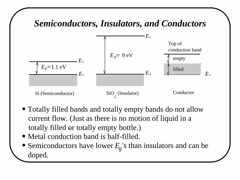
Semiconductors, Insulators, and Conductors
• Totally filled bands and totally empty bands do not allow
• Metal conduction band is half-filled.
E c
Ev
Eg=1.1 eV
E c
Eg= 9 eV empty
Si (Semiconductor) SiO2
(Insulator) Conductor
Ecfilled
Top ofconduction band
E v
current flow. (Just as there is no motion of liquid in a totally filled or totally empty bottle.).
• Semiconductors have lower Eg 's than insulators and can be doped.

Donor and Acceptor Levels in the Band Model
Conduction Band Ec
EvValence Band
Donor Level
Acceptor Level
Ed
Ea
Donor ionization energy
Acceptor ionization energy
Ionization energy of selected donors and acceptors in siliconAcceptors
Dopant Sb P As B Al InIonization energy, E c –E d or E a –E v (meV) 39 44 54 45 57 160
Donors
Hydrogen: Eionm0 q4
13.6 eV==8ε0
2h2

Dopants and Free Carriers
Dopant ionizationenergy ~50meV (very low).
Donorsn-type
Acceptorsp-type
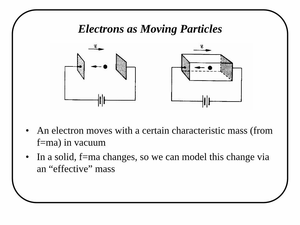
Electrons as Moving Particles
• An electron moves with a certain characteristic mass (from f=ma) in vacuum
• In a solid, f=ma changes, so we can model this change via an “effective” mass

Effective Mass
In an electric field, , an electron or a hole accelerates.
Electron and hole effective massesSi Ge GaAs GaP
m n /m 0 0.26 0.12 0.068 0.82m p /m 0 0.39 0.30 0.50 0.60
electrons
holes
Remember :F=ma=-qE
![FAN7711 Ballast Control Integrated Circuit - Digi-Key Sheets/Fairchild PDFs/FAN7711.pdf · FAN7711 Ballast Control Integrated Circuit) 1 3 0 circuit [.]](https://img.pdfslide.tips/doc/110x75/5acfdb947f8b9a1d328d8e40/fan7711-ballast-control-integrated-circuit-digi-key-sheetsfairchild-pdfsfan7711pdffan7711.jpg)


![Section 8 1-CCD.ppt [Λειτουργία συμβατότητας]tsiatouhas/CCD/Section_8_1-2p.pdf · 1 CMOSCMOS INTEGRATED INTEGRATED CIRCUIT DESIGN TECHNIQUES University of Ioannina](https://img.pdfslide.tips/doc/110x75/5adb58097f8b9a86378e87f8/section-8-1-ccdppt-tsiatouhasccdsection81-2ppdf1.jpg)