Embed Size (px)
Citation preview
ELECTRON BEAM STERILIZATION
NOR RUt HASMA BINTI ABDULLAH
Laporan projek ml dikemukakan sebagai memenuhi
sebahagian daripada syarat
penganugerahan Ijazah Sarjana Kejuruteraan Elektrik
Fakulti Kejuruteraan
Kolej Universiti Teknologi Tun. Hussein Onn
OKTOBER, 2004
UNVERSm M.4 LAYSiA PAI'ANG
No. Peroehan 1,4o. Parggi1an
034450 Tarikh
I.
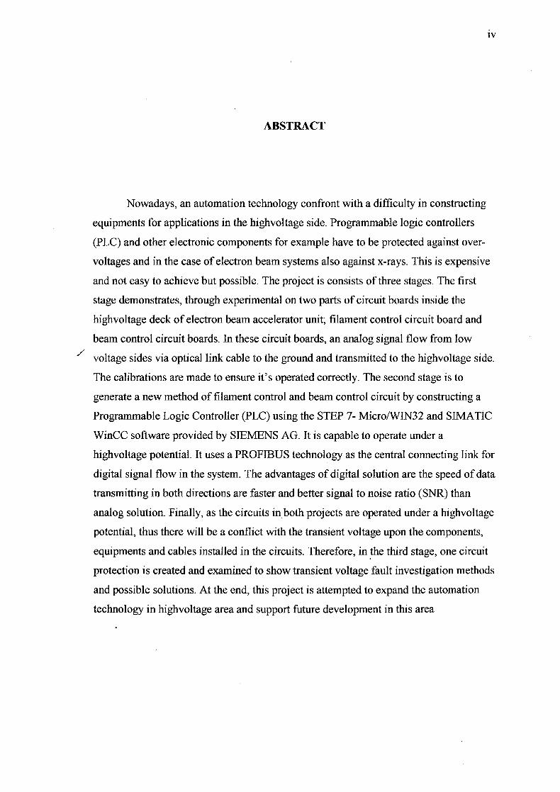
ABSTRACT
Nowadays, an automation technology confront with a difficulty in constructing
equipments for applications in the highvoltage side. Programmable logic controllers
(PLC) and other electronic components for example have to be protected against over-
voltages and in the case of electron beam systems also against x-rays. This is expensive
and not easy to achieve but possible. The project is consists of three stages. The first
stage demonstrates, through experimental on two parts of circuit boards inside the
highvoltage deck of electron beam accelerator unit; filament control circuit board and
beam control circuit boards. In these circuit boards, an analog signal flow from low
/ voltage sides via optical link cable to the ground and transmitted to the highvoltage side.
The calibrations are made to ensure it's operated correctly. The second stage is to
generate a new method of filament control and beam control circuit by constructing a
Programmable Logic Controller (PLC) using the STEP 7- Micro/W1N32 and SIMATIC
WinCC software provided by SIEMENS AG. It is capable to operate under a
highvoltage potential. It uses a PROFJBUS technology as the central connecting link for
digital signal flow in the system. The advantages of digital solution are the speed of data
transmitting in both directions are faster and better signal to noise ratio (SNR) than
analog solution. Finally, as the circuits in both projects are operated under a highvoltage
potential, thus there will be a conflict with the transient voltage upon the components,
equipments and cables installed in the circuits. Therefore, in the third stage, one circuit
protection is created and examined to show transient voltage fault investigation methods
and possible solutions. At the end, this project is attempted to expand the automation
technology in highvoltage area and support future development in this area
lv
ABSTRAK
Kini, teknologi automatifmenghadapi kesukaran dalam mengendalikan pelbagai
peralatan di kawasan bervoltan tinggi. "Programmable Logic Controller (PLC)" dan
peralatan elektonik yang lain sebagai contohnya hendaklah di dii indungi daripada voltan
lampau terutamanya untuk sistem sinaran elektronjuga sinar-x. Pembangunan projek
mi terbahagi kepada tiga peringkat. Peringkat awal projek rnelibatkan pengujian ke atas
dua buah papan litar yang akan dipasang di dalam "dek voltan tinggi", unit pemecut
sinaran elektron; litar kawalan filamen dan litar kawalan sinaran. Isyarat analog
digunakan sebagai agen penghantaran melalui kabel perhubungan optik dari bahagian
/ bervoltan rendah ke bumi sebelum di hantar ke bahagia n bervoltan tinggi.
Penentuukuran di laksanakan untuk memastikan kedua-dua litar beroperasi dengan tepat.
Peringkat kedua melibatkan penghasilan fungsi litar yang sama seperti peringkat
pertama tetapi dilaksanakan melalui kaedah yang baru iaitu dengan mengadaptasi PLC
menggunakan perisian STEP 7 Micro/W1N32 dan SIMATIC WinCC daripada
SIEMENS AG. la rnenggunakan teknologi PROFIBUS sebagai pusat rangkaian
perhubungan untuk isyarat digital dihantar di dalam sistern. Kelebihan isyarat digital
ialah kelajuan penghantaran data di kedua-dua arah dan isyarat-ke-hingar (SNR) lebili
baik daripada isyarat analog. Di sebabkan litar di kedua-dua projek terletak di bahagian
bervoltan tinggi, maka akan wujud permasaalah terhadap voltan lampau ke atas
komponen, peralatan dan kabel yang dipasang di dalam litar.OIeh itu di peringkat ketiga
projek, sebuah litar perlindungan dicipta dan diselidik untuk mengetahui pertahanan
terhadap voltan lampau dan penyelesaiannya. Akhirnya, projek mi berupaya
memperkembangkan penggunaan teknologi automatif ke bahagian bervoltan tinggi dan
menggalakkan penggunaannya di masa akan datang..
V
TABLE OFCONTAINS
vi
/
NO. TITLE PAGE
Acknowledgement ill
Abstract iv
Abstrak v
Table of Contains vi
List of Table xi
List of Figure xii
List of Abbreviation xvii
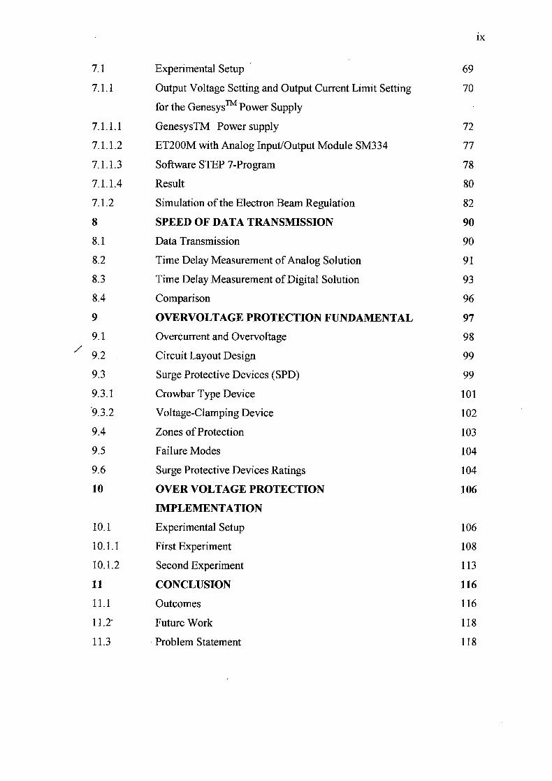
1 INTRODUCTION 1
1.1 Project Aim 1
1.2 Objective 1
1.3 Scope of the Project 2
1.4 Research Methodology 3
1.5 Literature Review 6
1.5.1 General Electron Beam 6
1.5.2 Electron Beam Application 7
1.5.2.1 Sterilization 8
1.5.2.2 Polymerization 8
1.5.2.3 Grafting 9
1.5.2.4 Crosslinking 10
1.5.2.5 Degradation 12
1.5.3 Electron Beam Accelerator 12
2 ELECTRON BEAM STERILIZATION 14
2.1 Project Background 14
V11
/
2.2 Electron Beam Sterilization System 16
2.3 Development of Electron Beam Accelerators 18
2.4 Advantages and Disadvantages 21
2.4 Analog and Digital Signal Transmission 22
2.4.1 Spark Discharges 23
2.4.2 Corona Discharges 24
2.4.3 X-radiation 24
3 PROFIBUS 26
3.1 PROFIBUS Technology 26
3.2 Communication Profiles 27
3.3 Physical Profiles 27
3.4 Basic Characteristics 28
3.5 DP Communication Profile 28
3.6 Device Engineering 29
3.6.1 GSD Files 29
3.7 Further Technical Developments 30
4 APPLICATION OF ANALOG SOLUTION 32
4.1 Circuit BOards Operation 32
4.2 What isRMS? 34
4.3 IDL 100 Data Logger (Intelligent Data Logger Collects 35
Information)
4.3.1 General Information 36
4.4 Function Generator 36
5 APPLICATION OF DIGITAL SOLUTION 37
5.1 Master and Slave 37
5.2 Hardware 38
5.2.1 Programmable Logic Controller (PLC) 39
5.2.1.1 PROFIBUS 40
5.2.1.1 S7400 40
5.2.1.3 ET200M 42
5.2.1.4 PROFIBUS Optical Bus Terminal (OBT) 44
viii
/
5.2.1.5 Inverter 45
5.2.1.6 GENESYS Power Supply 46
5.2.2 Programming Device 46
5.2.2.1 PG740 47
5.2.3 Cable 48
5.2.3.1 IvIPI 48
5.2.3.2 PROFIBUS Cable and Connector 48
5.3 Software 51
5.3.1 Software STEP 7 V 5.1 51
5.3.1.1 Programming Language 51
5.3.1.2 Programming Blocks 53
5.3.2 SIMATIC Windows Control Center (WinCC) 54
6 ANALOGUE SOLUTION IMPLEMENTATION 56
6.1 Filament Control Circuit Board 56
6.2 Experimental Set-up 57
6.2.1 Calibration of V/F Conversion 57
6.2.2 Calibration of FN Conversion 59
6.2.3 Temperature Dependence of FN conversion 60
6.2.3.1 Ceramic Capacitor 62
6.2.3.2 Extended Foil Polystyrene Capacitors 63
Type: EXFS/ HR
6.2.4 Measurement using AD650 (Voltage-to-Frequency and 65
Frequency-to-Voltage Converter)
6.2.4.1 Ceramic Capacitor 66
6.2.4.2 Extended Foil Polystyrene Capacitors 66
Type: EXFS/ HR
6.2.5 Comparison of Standard Ceramic Capacitor (C26) against 67
Extended Foil Polystyrene Capacitors Type EXFS/HR
between ADVC32H and AD650
6.3 Beam Control Circuit Board 67
7 DIGITAL SOLUTION iMPLEMENTATION 69
lx
/
7.1 Experimental Setup 69
7.1.1 Output Voltage Setting and Output Current Limit Setting 70
for the Genesys 'FM Power Supply
7.1.1.1 GenesysTM Power supply 72
7.1.1.2 ET200M with Analog Input/Output Module SM334 77
7.1.1.3 Software STEP 7-Program 78
7.1.1.4 Result 80
7.1.2 Simulation of the Electron Beam Regulation 82
8 SPEED OF DATA TRANSMISSION 90
8.1 Data Transmission 90
8.2 Time Delay Measurement of Analog Solution 91
8.3 Time Delay Measurement of Digital Solution 93
8.4 Comparison 96
9 OVERVOLTAGE PROTECTION FUNDAMENTAL 97
9.1 Overcurrent and Overvoltage 98
9.2 Circuit Layout Design 99
9.3 Surge Protective Devices (SPD) 99
9.3.1 Crowbar Type Device 101
9.3.2 Voltage-Clamping Device 102
9.4 Zones of Protection 103
9.5 Failure Modes 104
9.6 Surge Protective Devices Ratings 104
10 OVER VOLTAGE PROTECTION 106
IMPLEMENTATION
10.1 Experimental Setup 106
10.1.1 First Experiment 108
10.1.2 Second Experiment 113
11 CONCLUSION 116
11.1 Outcomes 116
11.2 Future Work 118
11.3 Problem Statement 118

11.3.1 Analog Solution
11.3.2 Overvoltage Protection
REFERENCE
118
119
121
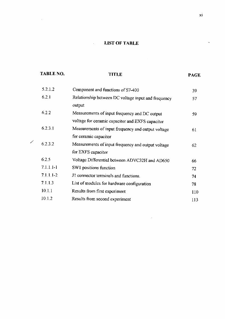
LIST OF TABLE
xi
/
TABLE NO. TITLE PAGE
5.2.1.2 Component and functions of S7-400 39 6.2.1 Relationship between DC voltage input and frequency 57
output
6.2.2 Measurements of input frequency and DC output 59
voltage for ceramic capacitor and EXFS capacitor
6.2.3.1 Measurements of input frequency and output voltage 61
for ceramic capacitor
6.2.3.2 Measurements of input frequency and output voltage 62
for EXFS capacitor
6.2.5 Voltage Differential between ADVC32H and AD650 66 7.1.1.1-1 SW1 positions function 72
7.1.1.1-2 Ji connector terminals and functions. 74 7.1.1.3 List of modules for hardware configuration 78
10.1.1 Results from first experiment 110
10.1.2 Results from second experiment 113
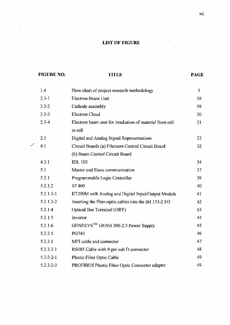
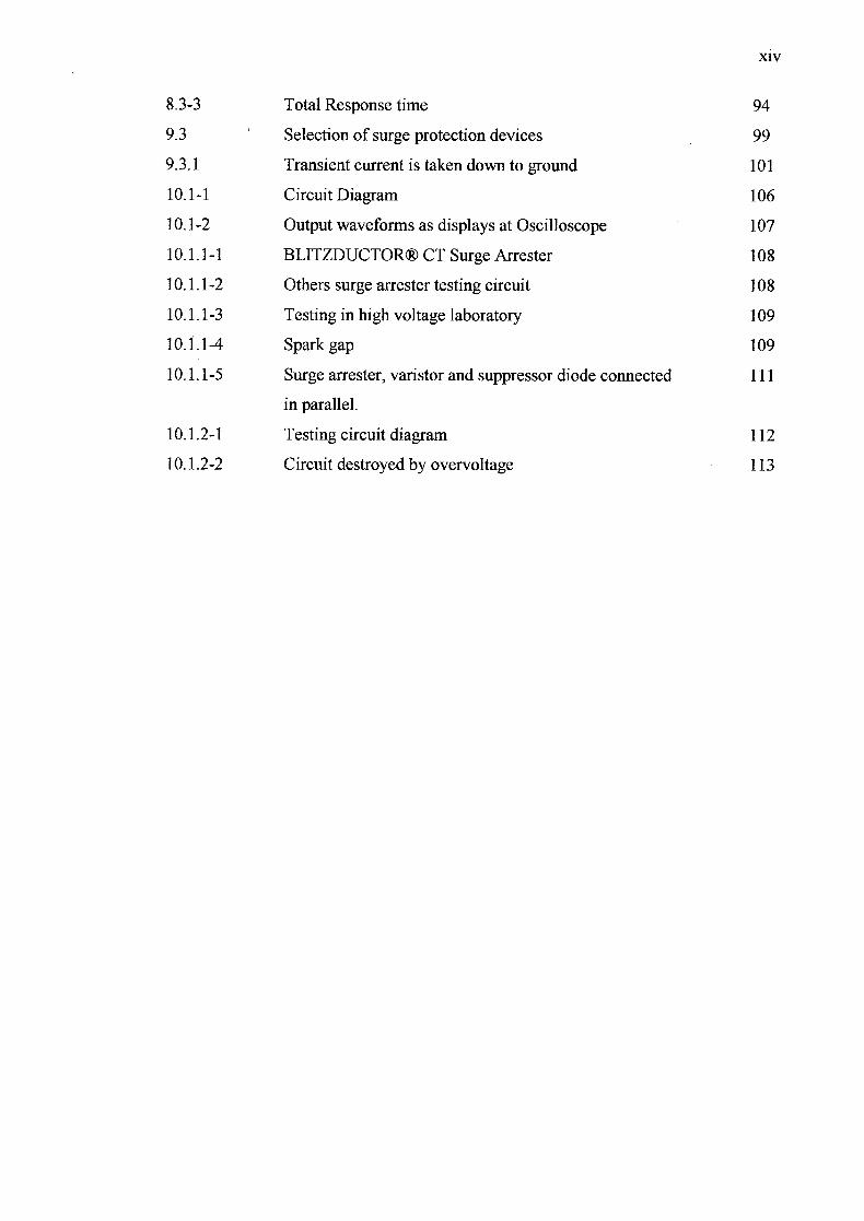
LIST OF FIGURE
FIGURE NO. TITLE PAGE
1.4 Flow chart of project research methodology 5
2.3-1 Electron Beam Unit 19
2.3-2 Cathode assembly 19
2.3-3 Electron Cloud 20
2.3-4 Electron beam unit for irradiation of material from roll 21
to roll
2.5 Digital and Analog Signal Representations 22 / 4.1 Circuit Boards (a) Filament Control Circuit Board 32
(b) Beam Control Circuit Board
4.3.1 IDL 100 34
5.1 Master and Slave communication 37
5.2.1 Programmable Logic Controller 39
5.2.1.2 S7400 40
5.2.1.3-1 ET200M with Analog and Digital Input/Output Module 41
5.2.1.3-2 Inserting the fiber-optic cables into the IIVI 153-2 FO 42
5.2.1.4 Optical Bus Terminal (OBT) 43
5.2.1.5 Inverter 44
5.2.1.6 GENESYS GENH 300-2.5 Power Supply 45
5.2.2.1 PG740 46
5.2.3.1 MIFf cable and connector 47
5.2.3.2-1 RS485 Cable with 9-pin sub D connector 48
5.2:3.2-1 Plastic Fiber Optic Cable 49
5.2.3.2-3 PROFIBUS Plastic Fiber Optic Connector adapter 49
xii
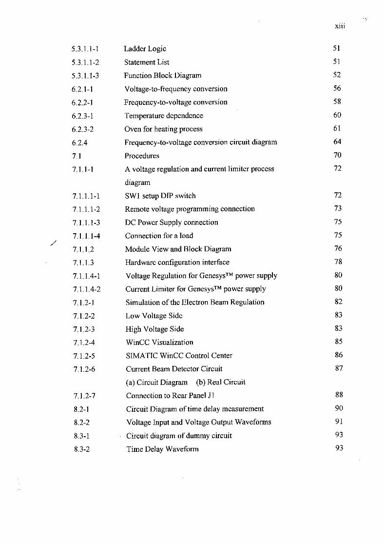
xiii
/
5.3.1.1-1 Ladder Logic 51
5.3.1.1-2 Statement List 51
5.3.1.1-3 Function Block Diagram 52
6.2.1-1 Voltage-to-frequency conversion 56
6.2.2-1 Frequency-to-voltage conversion 58
6.2.3-1 Temperature dependence 60
6.2.3-2 Oven for heating process 61
6.2.4 Frequency-to-voltage conversion circuit diagram 64
7.1 Procedures 70
7.1.1-1 A voltage regulation and current limiter process 72
diagram
7.1.1.1-1 SW1 setup DIP switch 72
7.1.1.1-2 Remote voltage programming connection 73
7.1.1.1-3 DC Power Supply connection 75
7.1.1.1-4 Connection for a load 75
7.1.1.2 Module View and Block Diagram 76
7.1.1.3 Hardware configuration interface 78
7.1.1.4-1 Voltage Regulation for GenesysTM power supply 80
7.1.1.4-2 Current Limiter for GenesysTM power supply 80
7.1.2-1 Simulation of the Electron Beam Regulation 82
7.1.2-2 Low Voltage Side 83
7.1.2-3 High Voltage Side 83
7.1.2-4 WinCC Visualization 85
7.1.2-5 SIMATIC WinCC Control Center 86
7.1.2-6 Current Beam Detector Circuit 87
(a) Circuit Diagram (b) Real Circuit
7.1.2-7 Connection to Rear Panel J 88
8.2-1 Circuit Diagram of time delay measurement 90
8.2-2 Voltage Input and Voltage Output Waveforms 91
8.3-1 Circuit diagram of dummy circuit 93
8.3-2 Time Delay Waveform 93
xlv
8.3-3 Total Response time 94
9.3 Selection of surge protection devices 99
9.3.1 Transient current is taken down to ground 101
10.1-1 Circuit Diagram 106
10.1-2 Output waveforms as displays at Oscilloscope 107
10.1.1-1 BLITZDUCTOR® CT Surge Arrester 108
10.1.1-2 Others surge arrester testing circuit 108
10.1.1-3 Testing in high voltage laboratory 109
10.1.1-4 Spark gap 109
10.1.1-5 Surge arrester, varistor and suppressor diode connected 111
in parallel.
10.1.2-1 Testing circuit diagram 112
10.1.2-2 Circuit destroyed by overvoltage 113
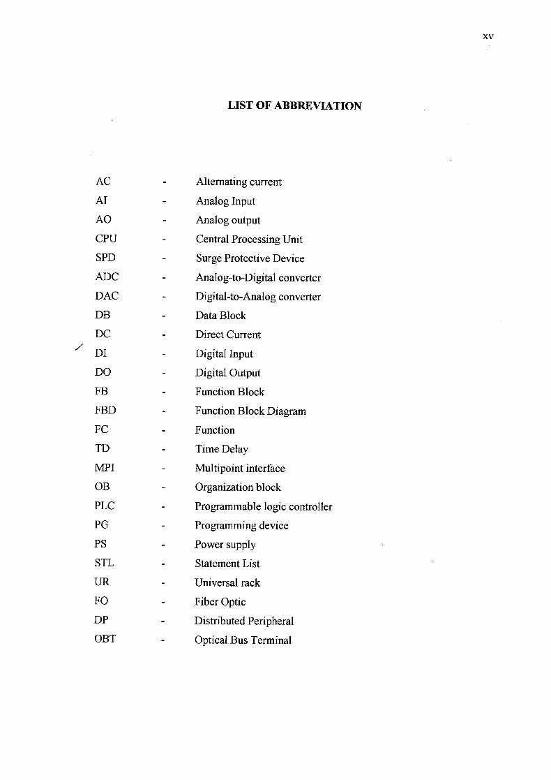
LIST OF ABBREVIATION
AC - Alternating current
Al - Analog Input
AO - Analog output
CPU - Central Processing Unit
SPD - Surge Protective Device
ADC - Analog-to-Digital converter
DAC - Digital-to-Analog converter
DB - Data Block
DC - Direct Current
/ DI - Digital Input
DO - Digital Output
FB - Function Block
FBD - Function Block Diagram
FC - Function
TD - Time Delay
MPJ - Multipoint interface
OB - Organization block
PLC - Programmable logic controller
PG - Programming device
PS - Power supply
STL - Statement List
UR - Universal rack
FO - Fiber Optic
DP - Distributed Peripheral
OBT - Optical Bus Terminal
xv
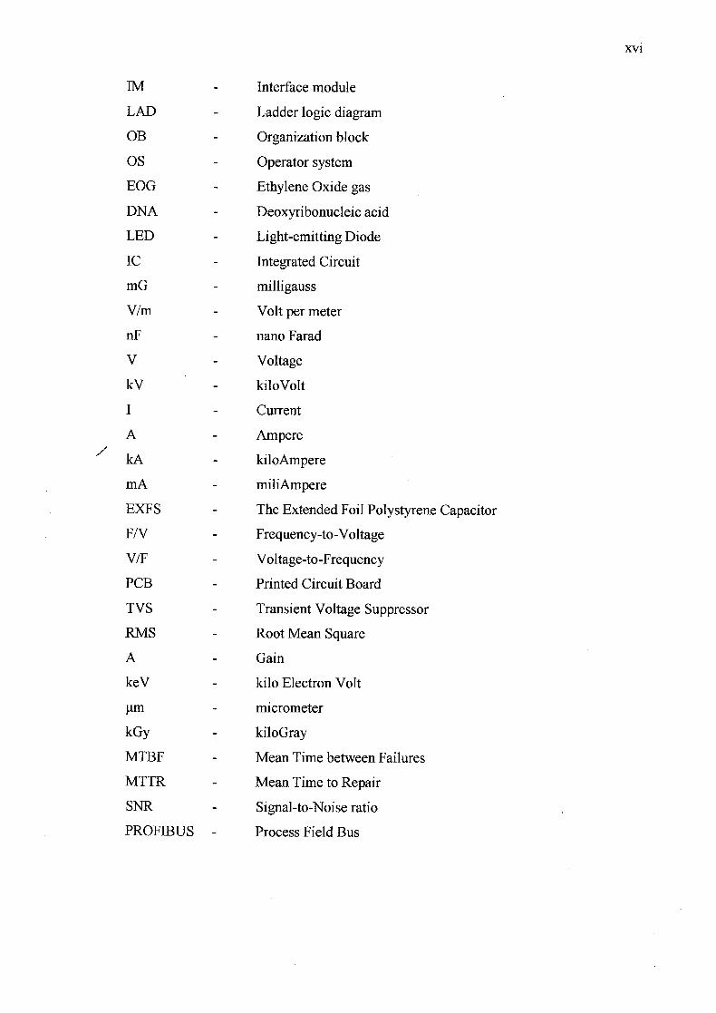
xvi
IM - Interface module
LAD - Ladder logic diagram
OB - Organization block
OS - Operator system
EOG - Ethylene Oxide gas
DNA - Deoxyribonucleic acid
LED - Light-emitting Diode
IC - Integrated Circuit
mG - milligauss
V/rn - Volt per meter
nF - nano Farad
V - Voltage
kV - kiloVolt
I - Current
A - Ampere / kA - kiloAmpere
mA - miliAmpere
EXFS - The Extended Foil Polystyrene Capacitor
F/V - Frequency-to-Voltage
V/F - Voltage-to-Frequency
PCB - Printed Circuit Board
TVS - Transient Voltage Suppressor
RMS - Root Mean Square
A - Gain
keV - kilo Electron Volt
pm - micrometer
kGy - kiloGray
MTBF - Mean Time between Failures
MTTR - Mean Time to Repair
SNR - Signal-to-Noise ratio
PROFIBUS - Process Field Bus
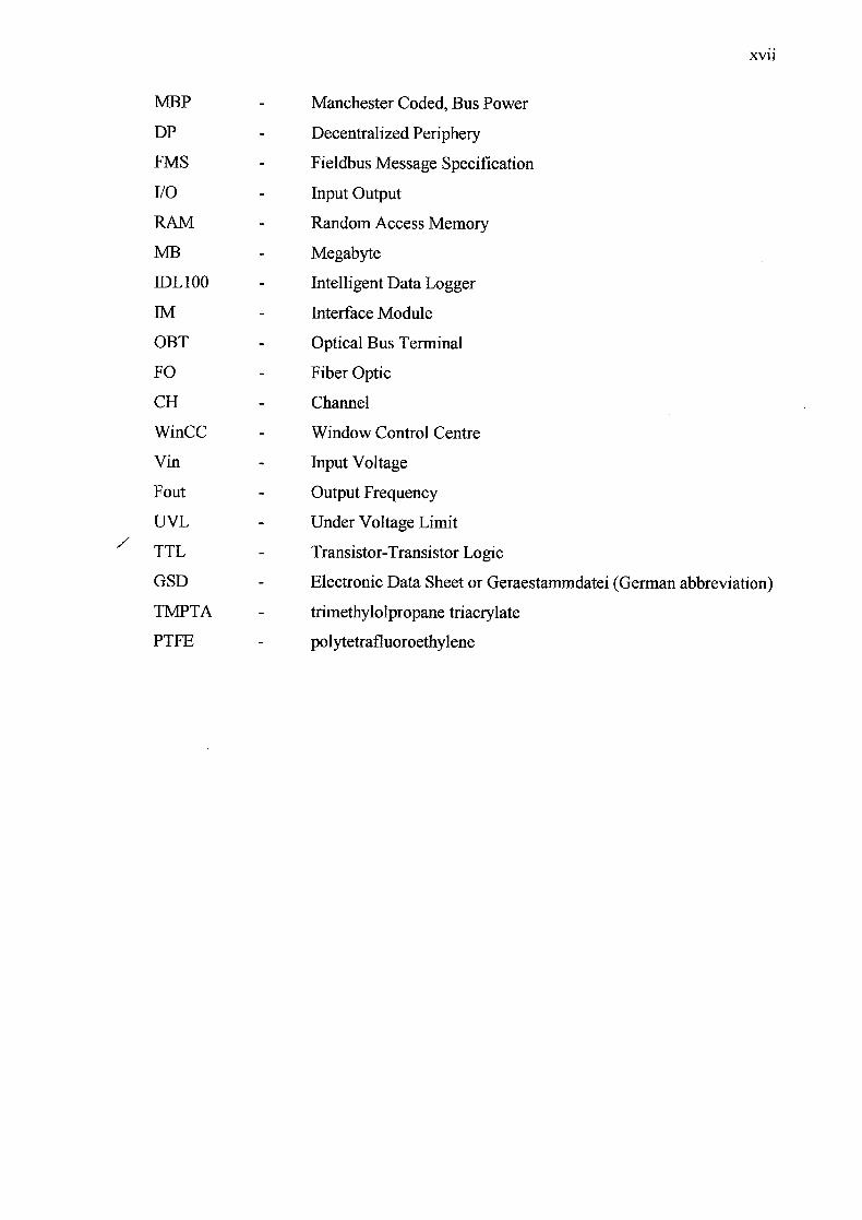
xvii
MBP - Manchester Coded, Bus Power
DP - Decentralized Periphery
FMS - Fieldbus Message Specification
110 - Input Output
RAM - Random Access Memory
MB - Megabyte
IDL 100 - Intelligent Data Logger
ilvI - Interface Module
OBT - Optical Bus Terminal
FO - Fiber Optic
CH - Channel
WinCC - Window Control Centre
Vin - Input Voltage
Fout - Output Frequency
UVL - Under Voltage Limit / TTL - Transistor-Transistor Logic
GSD - Electronic Data Sheet or Geraestammdatei (German abbreviation)
TMPTA - trimethylolpropane triacrylate
PTFE - polytetrafluoroethylene
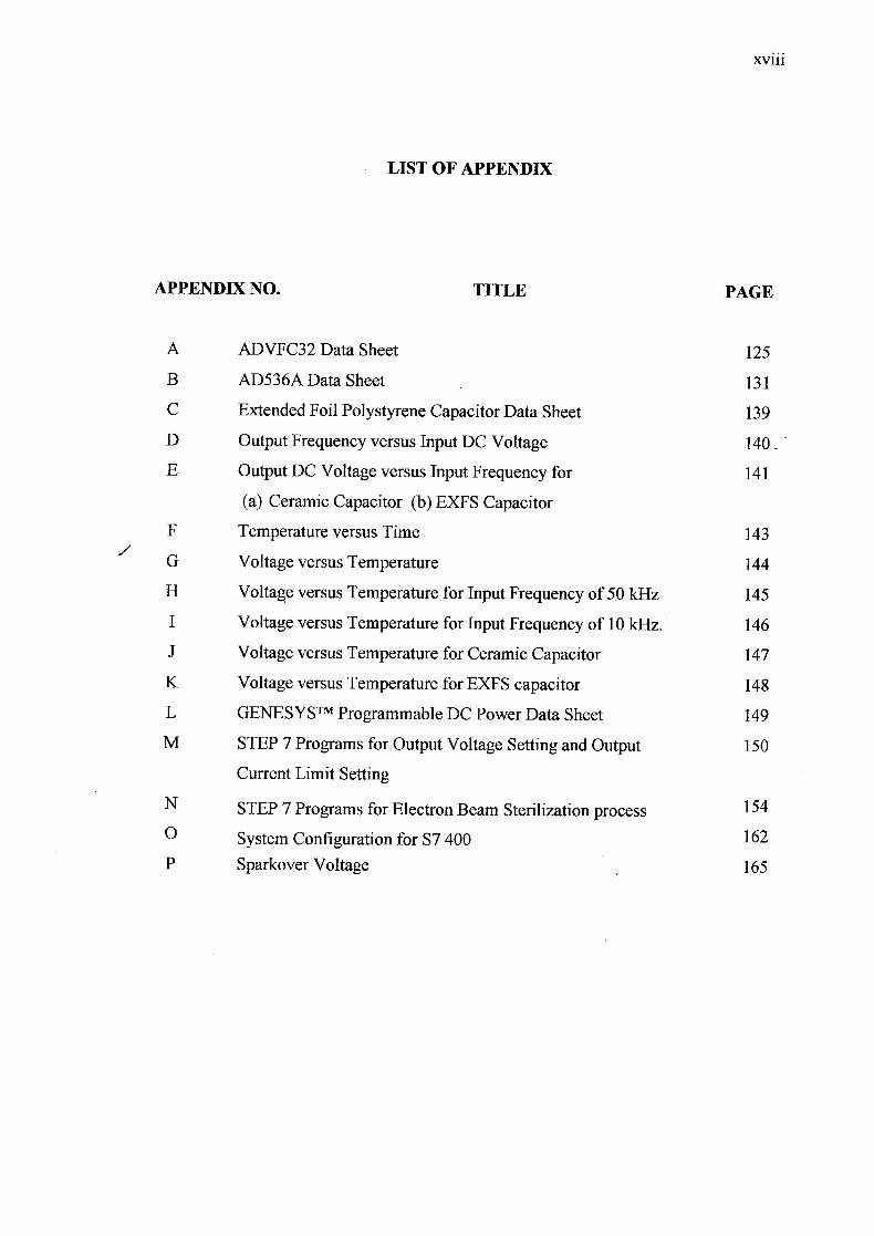
LIST OF APPENDIX
xviii
/
APPENDIX NO. TITLE PAGE
A ADVFC32 Data Sheet 125
B AD536AData Sheet 131
C Extended Foil Polystyrene Capacitor Data Sheet 139
D Output Frequency versus Input DC Voltage 140,
E Output DC Voltage versus Input Frequency for 141
(a) Ceramic Capacitor (b) EXFS Capacitor
F Temperature versus Time 143
G Voltage versus Temperature 144
H Voltage versus Temperature for Input Frequency of 50 kHz 145
I Voltage versus Temperature for Input Frequency of 10 kHz. 146
J Voltage versus Temperature for Ceramic Capacitor 147
K Voltage versus Temperature for EXFS capacitor 148
L GENESYSTM Programmable DC Power Data Sheet 149
M STEP 7 Programs for Output Voltage Setting and Output 150
Current Limit Setting
N STEP 7 Programs for Electron Beam Sterilization process 154
System Configuration for S7 400 162
P Sparkover Voltage 165
CHAPTER I
INTRODUCTION
This chapter is described about the project's introduction. It consists of
objectives, scopes of the project, methodology and literature review.
1.1 Project Aim
The project aims are to compare the performance between the conventional circuits
of filament control and beam control circuit boards with a new application of electron
beam regulation using a standard components and worked correctly under a high voltage
potential.
1.2 Objective
The primary objectives of this thesis are threefold. The first objective is to
analyze the operation of a new filament control and beam control circuit boards inside
the High Voltage Deck of electron beam sterilization unit whether it's running with the
/
correct operation. In this conventional method, data is transmitted or received in analog
2
signal between low voltages to high voltage side. The second objective is to generate a
new method of filament control and beam control circuit by constructing a
Programmable Logic Controller (PLC) that capable to operate in a high voltage side
using standard equipments such as ET200M, PROFIBUS cables, Analog Digital
Converter (ADC) or Digital Analog Converter (DAC) and others. The most important
thing, it uses a PROFIBUS technology as the central connecting link for signal flow in
the system. Hence, this method is compared whether it working similar or had a better
performance than the conventional method. The third objective is to determine the
effects of electric and magnetic fields generated by surge voltage or transient voltage on
electronic measuring circuits for both methods. Therefore finding out the means for
protecting or decreasing the effects of such interferences by choosing the suitable surge
protective devices installed into the circuits.
/ 13 Scope Of The Project
Scope of the project will be converging into a circuit board assembly that consist
of filament control and beam control circuit board. A test is implemented to ensure a
correct circuit operation as it been upgraded with a modem electronic devices to have a
better availability rather than the old circuit boards. Then, it is concentrated in
constructing a simulation of electron beam regulation using PLC with PROFIBUS
communication protocol, STEP 7 and SIMATIC WinCC software, ET200M with
ADC/DAC and tested under high voltage potential without generated an error in data
transmission. Finally, the project is focus on a protection of a dummy circuit created
against surge voltage in a High Voltage Laboratory.
3
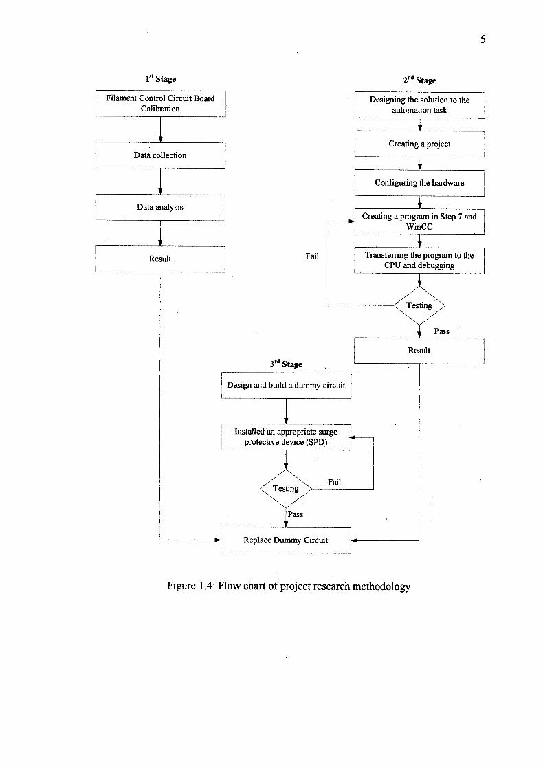
1.4 Research Methodology
Research is needed to define and evaluate suitable methodologies and technique in
order to identify and specify the accuracy of the instrumentations performed by using
exact procedure shows in Fig. 1.4. The procedures are divided into a three different
stages to ensure the proper implementations are established. The project method firstly
established by calibration of the filament control circuit board for two type of capacitor
and compared the performance of the circuit board upon the variation of a temperature.
There are several kinds of experiments that have been accomplished during these
calibrations. It consists of an experimentation of a voltage-to-frequency conversion and
frequency-to-voltage conversion as the frequency of the filament set will be in the range
of 10 kHz to lOOk Hz with DC voltage varying from OV to 1OV and vice versa. It is
important as the circuit will be located under a high voltage potential and confront with
temperature arising cause by spark, corona or x-radiation. The temperature sensor is
/ attached to capacitor for collecting the temperature variation and directly wired to Data
Logger for collection a data. Also, the voltage probe is installed at Pin 7 TL084P to
record the voltage value as the temperature varied Using the data logger software,
ICP 100 the data is downloaded to the computer and exported to a spreadsheet
application such as Microsoft Excel for a data analysis.
In a second stage, the project implementations began by determined the automation
task. The tasks are; to set the voltage regulation and current limiter for the GENESYSTM
power supply by adjusted the DC power supply remotely and;. to simulate the electron
beam regulation using a STEP 7 software and SJMATIC WinCC. The project is created
with the SIMATIC Manager as the central window which becomes active when STEP 7
is started. The project structure is used to store and arrange all the data and programs in
order. Thus, after created a project with SIMATIC station the hardware used for the
project is configured such as PLC, Programming Device, Programming Software and
Connector Cable are assemble on the rail. The hardware is configured with STEP 7.
These configuration data are transferred to the programmable controller later on
"downloading". After the hardware connection is finished, then a software STEP 7-
El
Program is required in order to inform the PLC what instructions it must follow. The
program is created in a standard language Statement List (STL) rather than Ladder Logic
or Function Block Diagram. Thus, before download the program, we have to make sure
the entire components already establish an online connection to the central processing
unit (CPU), the CPU is in RUN or RUN-P mode, and the program is downloading. In
STEP 7, OB 1 is processed cyclically by the CPU. The CPU reads line by line and
executes the program commands. When the CPU returns to the first program line, it has
completed exactly one cycle. The STEP 7 programs of this project are included
organization block (OB), function block (FB) and data block (DB). In an extreme case,
the CPU goes into STOP while processing an S7 program, or the switch of the CPU not
in a RUN mode after downloaded the program. The cause of the error is determined
from the events listed in the diagnostic buffer.
Finally in the third stage, for an overvoltage protection system; a dummy circuit that
consist a combination of integrator and Schmidt Trigger is designed. The experiment is
not implemented to the original circuit used in stage 1 and 2 because the possibility of
damaging the circuit is high. The original circuits or equipment are complicated and the
components used are expensive. Therefore, it is more convenient if using a circuit which
are easy to recreate and cheaper than the original circuits. Furthermore, if this
experiment is able to protect the dummy circuit, then it also possible to protect others
circuits. An appropriate surge protective device is installed in Zone 1 and 3 as the circuit
protection and the experimental is conducted inside a high voltage laboratory for spark
over tested. If the experiment is failed in protecting the dummy circuit, the experiment is
started again by replaced the surge protective device or reconstructed the protection
circuit. If the experiment is successfully protected the dummy circuit, therefore the
replacement of the dummy circuit with a circuits in stage 1 and 2 can be accomplish.
I" Stage
Filament Control Circuit Board 1 Calibration
Data collection
Data analysis
Result
2nd Stage
Designing the solution to the automation task
Creating a project
Configuring the hardware
, Creating a program in Step 7 and WinCC
Fail Transferring the program to the1 CPU and debugging
Testing
Pass
Result 3rd Stage
Design and build a dummy circuit
Installed an appropriate surge protective device (SPD)
TestingFail
Pass
Replace Dummy Circuit
Figure 1.4: Flow chart of project research methodology
1.5 Literature Review
1.5.1 General Electron Beam
For over sixty years the physical and chemical changes induced by absorption of
radiation sufficiently high in energy to produce ionization have been the subject of both
university and industrial research. At this time, the most common commercial sources of
ionizing radiation are 60Co and 137Cs for gamma irradiation and electron accelerators for
e-beam (beta) irradiation (Singh and Silverman, 1992). When the electron-beam
generated by an accelerator is directed at a target consisting of a high-atomic-number
metal, such as tungsten, X-rays with a broad spectrum of energies can also be produced.
Industrial irradiation processes using high-power electron accelerators are attractive
/ because the throughput rates are very high and the treatment costs per unit of product are
often competitive with more conventional chemical processes. The utilization of energy
in electron beam processing is more efficient than typical thermal processing. The
energy is delivered directly to the molecules, thus there is no need to heat the material in
ovens or tools, or to allow for permeation of chemicals into the material being
processed. The use of volatile or toxic chemicals can be avoided. Strict temperature or
moisture controls may not be needed. Irradiated materials are useable immediately after
processing. These capabilities are unique in that beneficial changes can be induced
rapidly in solid materials and preformed products. The amount of electron beam
radiation absorbed by the target is referred to as the dose, which is typically defined in
terms of kiloGrays (where 1 kGy= 1000 J/kg) or MegaRads (where 1 MRad=1,00O,O0O
erg/g) (Bly, 1988). The number of electrons emitted per unit of time is dependant upon
the power of the electron accelerator. This is expressed in kW. According to the
treatment to be carried out, the power of the electron beam may vary from 10 to several
hundreds of kW, for energy of 5 to 10 MeV.
/
7
1.5.2 Electron Beam Application
Crosslinking plastic materials, sterilizing medical products or packaging material
and preserving foods were the earliest developments of electron beam processing.
Processes for curing monomeric coatings and inks were developed somewhat later. The
use of these and other processes has grown and they are widely practiced today. Electron
beam crosslinking is used to produce heat-shrinkable plastic films for packaging foods
and other consumer products, heat-shrinkable plastic tubing, heat-shrinkable plastic film
and plastic pipe. The insulation on electrical wires and the jackets on multi-conductor
cables are crosslinked to increase heat tolerance and to improve the resistance to
abrasion and solvents. Crosslinked plastic pipe is used for hot water distribution
systems. Radiation cured, solvent-free coatings and inks are used for magazines,
newspapers and a variety of packaging materials.
All forms of ionizing radiation interact with matter by transferring energy to the
electrons orbiting the atomic nuclei of target materials. These electrons may then be
either released from the atoms, yielding positively charged ions and free electrons, or
moved to a higher-energy atomic orbital, yielding and excited atom or molecule. These
ions, electrons, and excited species are the precursors of any chemical changes observed
in irradiated material (Cooper, Curry and O'Shea, 1998). Thus, by using ionizing
radiation, it is possible to synthesize, modify, crosslink, and degrade polymers. Electron
beam radiation is a distinct and efficient means of bringing about controlled beneficial
changes in polymeric systems. These beneficial changes include increases in modulus,
tensile and impact strength, hardness, deflection and service temperature, stress-crack
resistance, abrasion resistance, creep and fatigue resistance, and barrier properties
(Gehring and ZybaIl, 1995). In the polymerization for composites material, doses are
usually in the range of 100 to 200 kGy (Berejka and Eberle, 2002, Kerluke and Cheng,
2002). Electron-beam processing offers significant improvements in processing
technique, curing time and cost.
8
1.5.2.1 Sterilization
Likewise, ionizing radiation has the ability to break the chains of DNA in living
organisms, such as bacteria, resulting in microbial death and rendering the space they
inhabit sterile (Bly, 1988). During last years the electron beam treatment is more and
more widely used for the sterilization of various medical devices and preparations. The
electron beam sterilization of disposal syringes is now a norm. But not only syringes, but
the single use devices for blood exchange, gynecologic endings, gloves, disposal cloths
for operations, are now sterilized by electron beam (Auslender, 1994). The machines
with electron energy of 10 MeV are usually used for these purposes. These machines are
rather complicated and expensive. The Budker Institute for Nuclear Physics has
designed and supplied irradiation facilities operating in many countries. One of the
supplies is the automated installation for sterilization of single-use syringes working in
the city of Izhevsk, Russia (Auslender, Polyakov and Golnik, 1993): The technology for
sterilization of syringes permitted to use the electron beam with energy of 2.5-4 MeV.
One of the main technological problems of electron beam sterilization of syringes is the
achievement of maximum possible homogeneity of dose distribution. The high dose
inhomogeneity leads to low quality of sterilization, as the lower dose limit 25 kGy is
determined by the resistivity of microbes, and the greater dose leads to sufficient
degradation of mechanical properties of plastic syringes.
1.5.2.2 Polymerization
(a) Coatings, Adhesives and Inks
Solvent-free coatings, adhesives and inks are cured (polymerized) by treatment with
low-energy electron beams. These materials are combinations of oligomers
(polymers with low molecular weights) and monomers, which control the viscosity
before curing. Volatile solvents are not needed and curing occurs without loss of
material. Typical oligomers are acrylated urethane polyesters, acrylated epoxies and
polyethers. A typical multifunctional monomer is trimethyloipropane tnacrylate
(TIvIPTA). Dose requirements are relatively low, in the range of 10 to 30 kGy, and
line speeds as high as 1500 m/min are achievable at 10 kGy with high-current, low-
energy, multiple-beam electron accelerators (Nablo and Tripp, 1977).
(b) Composite Materials
Fibre-reinforced composite materials are used where greater strength is needed.
Such materials are usually cured with heat, but electron-beam curing offers
significant improvements in processing technique, curing time and cost. Typical
materials are acrylated epoxies with carbon fibers. Doses are usually in the range of
100 to 200 kGy (Berejka and Eberle, 2002, Kerluke and Cheng, 2002). Initial
formulations are mixtures of oligomers and monomers. The radiation curing process
involves a combination of polymerization and crosslinking. The main applications
are in automotive and aerospace industries.
1.5.2.2 Grafting
Grafting is polymerizes a monomer onto the polymer chain; modifies the surface
properties of a polymer substrate; introduces new functionalities. The surface properties
of polymers can be modified by graft copolymerization with different monomers
(Chapiro, 1962). Grafting can be accomplished by electron beam irradiation on common
polymers such as polyethylene, polypropylene and fluoropolymers. Most work has been
done on polymer films, membranes, fibers and natural and synthetic textiles. Some
examples of monomers that can be grafted onto polytetrafluoroethylene (PTFE) films
are styrene, acrylic acid, 4-vinylpyridine and Nvinylpyrrolidone (Chapiro, 1977). Other
applications include ion exchange membranes, fuel cell/battery separator films,
permeation separation membranes, surface adhesion promotion, chelating fibers for sea-
10
water treatment and recovering of precious metals, etc. Some dose requirements may be
less than 10 kGy.
1.5.2.4 Crosslinking
Crosslinking is the most important effect of polymer irradiation because it can
usually improve the mechanical and thermal properties and chemical, environmental and
radiation stabilities of preformed parts as well as bulk materials. It forms a network
among the polymer chains and increases the molecular weight; improves temperature
resistance, chemical resistance, and mechanical properties; Both polymer crosslinking
and degradation by chain scission occur during treatment, but one or the other of these
effects may be predominant in some materials (Silverman, 1981;Charlesby, 1977).
Typical dose requirements for crosslinking are in the range of 50 to 150 kGy. Additives,
typically multifunctional monomers, may be mixed with the basic polymer to enhance
the crosslinking effect and reduce thô dose requirement. Antioxidants, UV stabilizers
and flame retardants may also be added to meet industrial performance specifications.
Such additives may reduce the crosslinking effect. So, the properties of commercial
compounds may be different from those of pure polymers.
(a) Insulated Wire and Cable
The crosslinking of insulation on electrical wires and cables was one of the first
practical applications of electron beam processing. It was introduced by the
Raychem Corporation during the 1950s, and it has been adopted by many other
manufacturers since then. Some polymers used in this application are polyethylene,
polyvinylchloride, ethylene-propylene rubber, polyvinylidene fluoride, and ethylene
tetrafluoroethylene copolymer. Product improvements obtained by irradiation
include increased tolerance to high temperature environments and overloaded
conductors, fire retardation, increased abrasion resistance and tensile strength,