Embed Size (px)
Citation preview
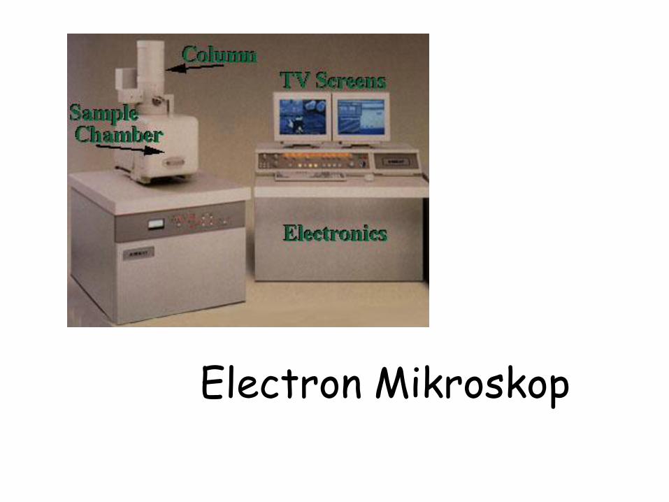
Electron Mikroskop
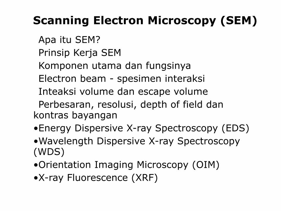
Scanning Electron Microscopy (SEM)
•Apa itu SEM?
•Prinsip Kerja SEM
•Komponen utama dan fungsinya
•Electron beam - spesimen interaksi
•Inteaksi volume dan escape volume
•Perbesaran, resolusi, depth of field dan kontras bayangan
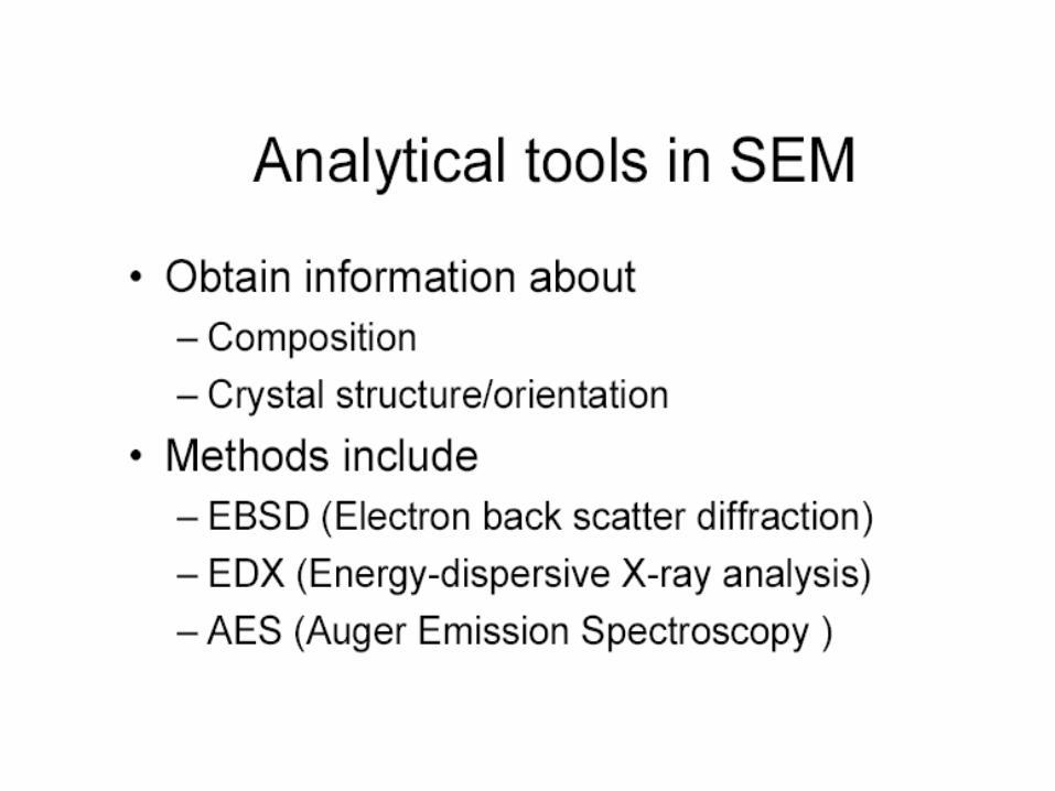
•Energy Dispersive X-ray Spectroscopy (EDS)
•Wavelength Dispersive X-ray Spectroscopy (WDS)
•Orientation Imaging Microscopy (OIM)
•X-ray Fluorescence (XRF)
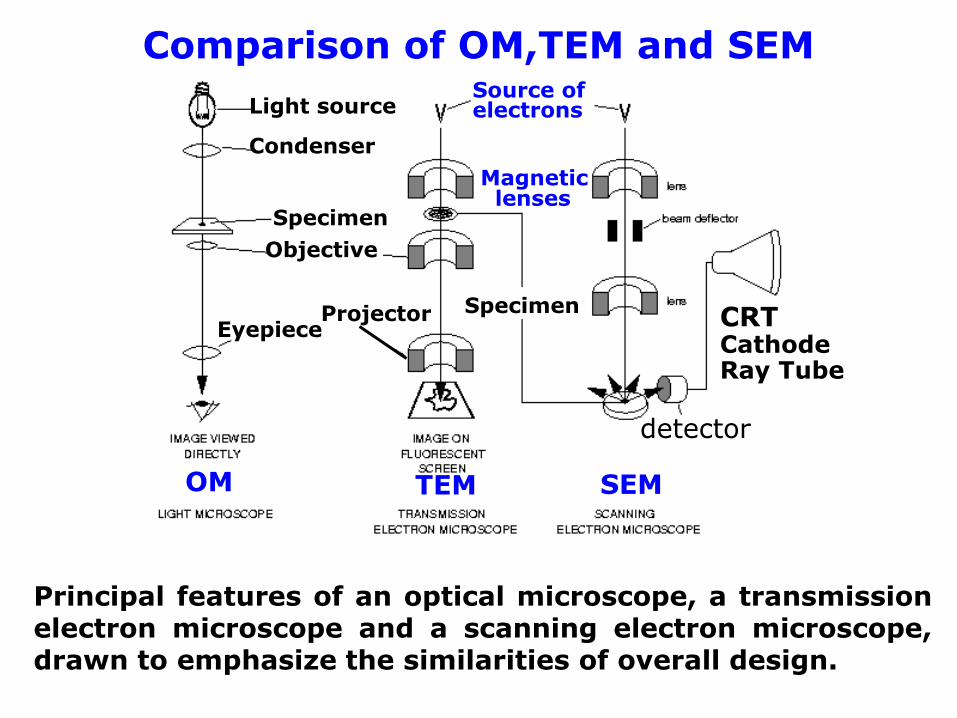
Principal features of an optical microscope, a transmissionelectron microscope and a scanning electron microscope,drawn to emphasize the similarities of overall design.
Comparison of OM,TEM and SEM
OM TEM SEM
Magneticlenses
detector
CRTCathode Ray Tube
Light sourceSource of electrons
Condenser
Specimen
Objective
EyepieceProjector Specimen
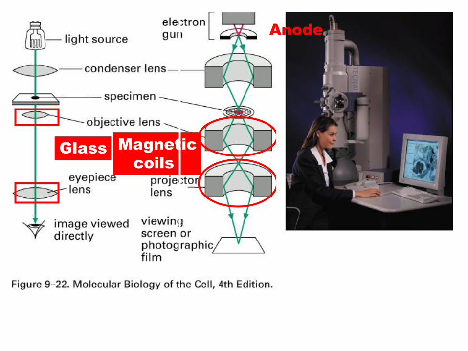
Glass Magnetic
coils
Under vacuum
Anode
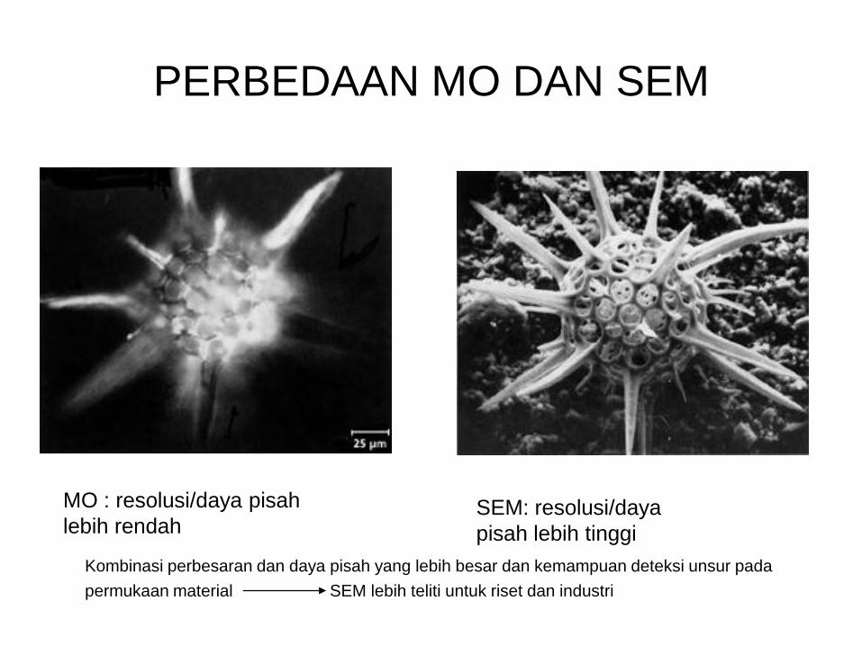
PERBEDAAN MO DAN SEM
MO : resolusi/daya pisah
lebih rendahSEM: resolusi/daya
pisah lebih tinggi
Kombinasi perbesaran dan daya pisah yang lebih besar dan kemampuan deteksi unsur pada
permukaan material SEM lebih teliti untuk riset dan industri
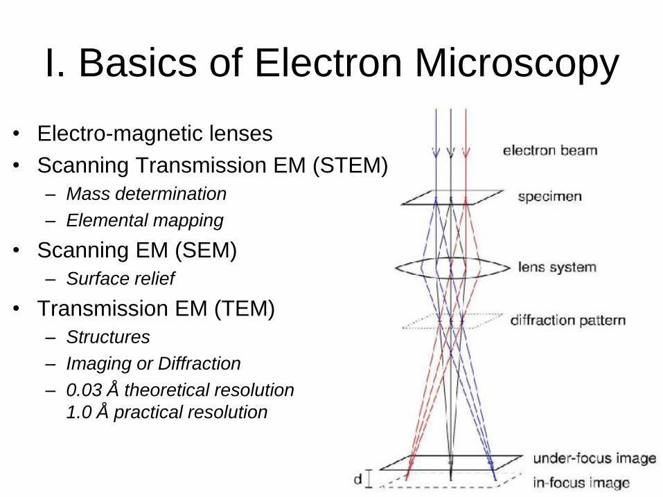
I. Basics of Electron Microscopy
• Electro-magnetic lenses
• Scanning Transmission EM (STEM)
– Mass determination
– Elemental mapping
• Scanning EM (SEM)
– Surface relief
• Transmission EM (TEM)
– Structures
– Imaging or Diffraction
– 0.03 Å theoretical resolution
1.0 Å practical resolution
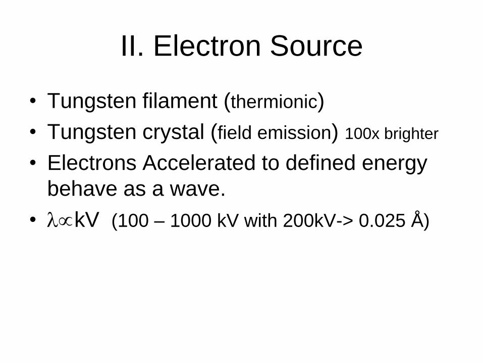
II. Electron Source
• Tungsten filament (thermionic)
• Tungsten crystal (field emission) 100x brighter
• Electrons Accelerated to defined energy
behave as a wave.
• kV (100 – 1000 kV with 200kV-> 0.025 Å)
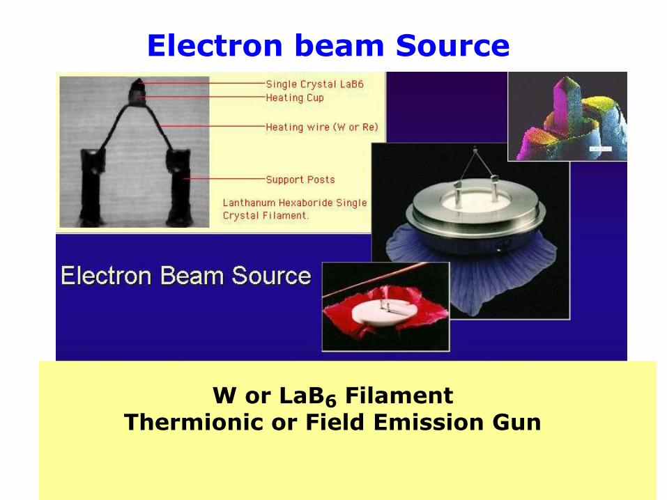
Electron beam Source
W or LaB6 FilamentThermionic or Field Emission Gun
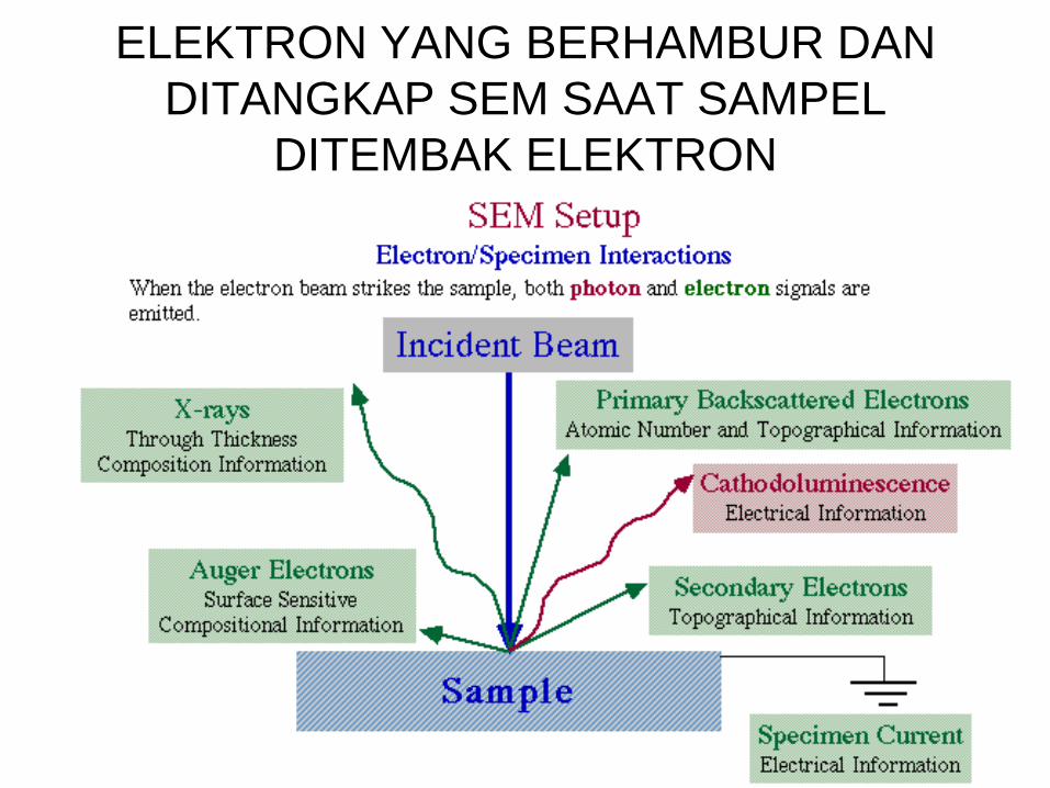
ELEKTRON YANG BERHAMBUR DAN
DITANGKAP SEM SAAT SAMPEL
DITEMBAK ELEKTRON
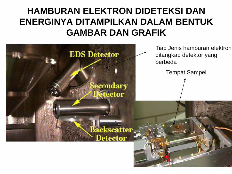
HAMBURAN ELEKTRON DIDETEKSI DAN
ENERGINYA DITAMPILKAN DALAM BENTUK
GAMBAR DAN GRAFIK
Tempat Sampel
Tiap Jenis hamburan elektron
ditangkap detektor yang
berbeda
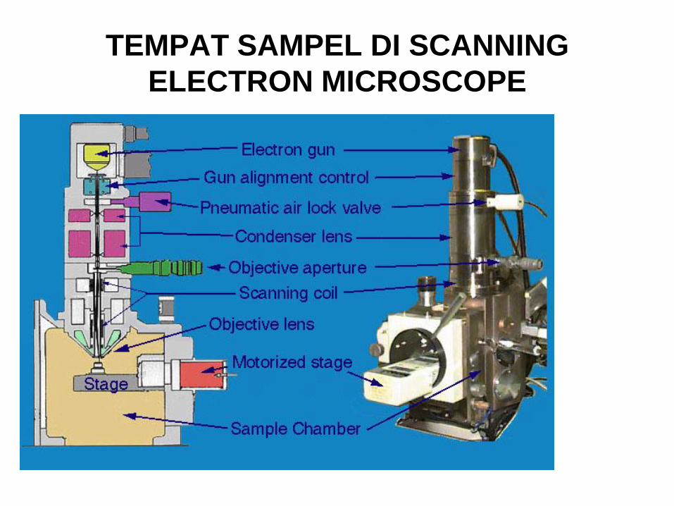
TEMPAT SAMPEL DI SCANNING
ELECTRON MICROSCOPE
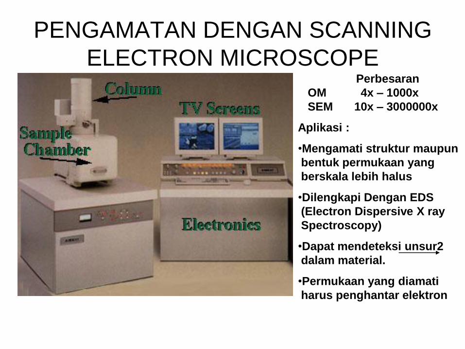
PENGAMATAN DENGAN SCANNING
ELECTRON MICROSCOPEPerbesaran
OM 4x – 1000x
SEM 10x – 3000000x
Aplikasi :
•Mengamati struktur maupun
bentuk permukaan yang
berskala lebih halus
•Dilengkapi Dengan EDS
(Electron Dispersive X ray
Spectroscopy)
•Dapat mendeteksi unsur2
dalam material.
•Permukaan yang diamati
harus penghantar elektron
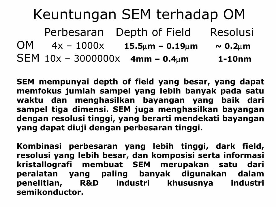
Keuntungan SEM terhadap OMPerbesaran Depth of Field Resolusi
OM 4x – 1000x 15.5mm – 0.19mm ~ 0.2mm
SEM 10x – 3000000x 4mm – 0.4mm 1-10nm
SEM mempunyai depth of field yang besar, yang dapatmemfokus jumlah sampel yang lebih banyak pada satuwaktu dan menghasilkan bayangan yang baik darisampel tiga dimensi. SEM juga menghasilkan bayangandengan resolusi tinggi, yang berarti mendekati bayanganyang dapat diuji dengan perbesaran tinggi.
Kombinasi perbesaran yang lebih tinggi, dark field,resolusi yang lebih besar, dan komposisi serta informasikristallografi membuat SEM merupakan satu dariperalatan yang paling banyak digunakan dalampenelitian, R&D industri khususnya industrisemikonductor.
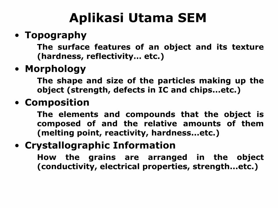
Aplikasi Utama SEM
• Topography
The surface features of an object and its texture(hardness, reflectivity… etc.)
• Morphology
The shape and size of the particles making up theobject (strength, defects in IC and chips...etc.)
• Composition
The elements and compounds that the object iscomposed of and the relative amounts of them(melting point, reactivity, hardness...etc.)
• Crystallographic Information
How the grains are arranged in the object(conductivity, electrical properties, strength...etc.)
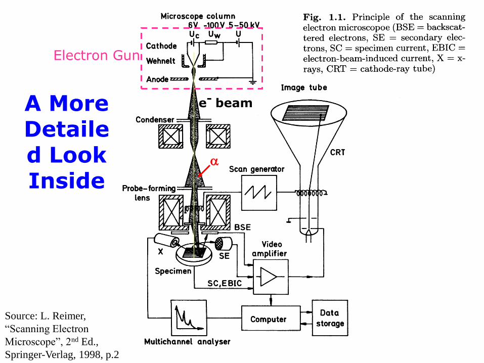
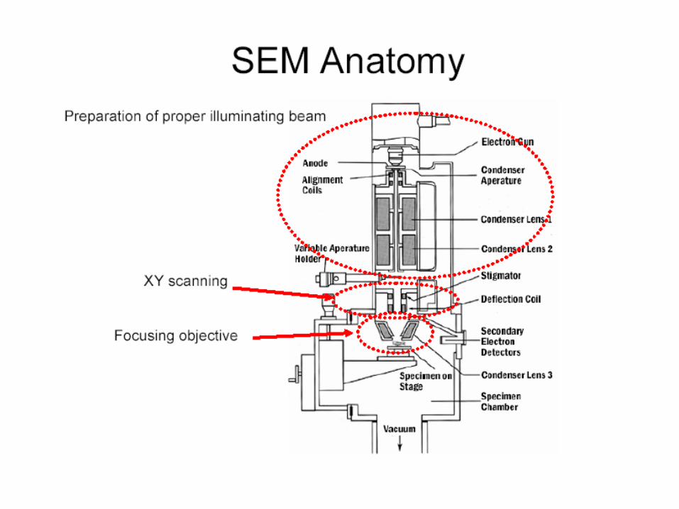
A More Detailed Look Inside
Source: L. Reimer,
“Scanning Electron
Microscope”, 2nd Ed.,
Springer-Verlag, 1998, p.2
Electron Gun
e- beam
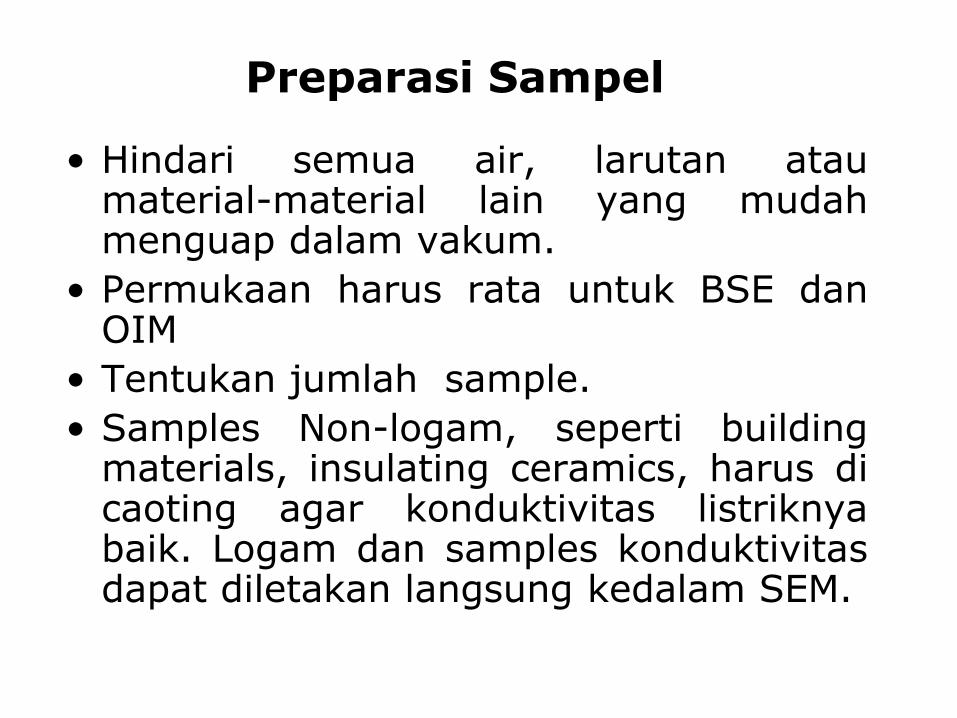
Preparasi Sampel
• Hindari semua air, larutan ataumaterial-material lain yang mudahmenguap dalam vakum.
• Permukaan harus rata untuk BSE danOIM
• Tentukan jumlah sample.
• Samples Non-logam, seperti buildingmaterials, insulating ceramics, harus dicaoting agar konduktivitas listriknyabaik. Logam dan samples konduktivitasdapat diletakan langsung kedalam SEM.
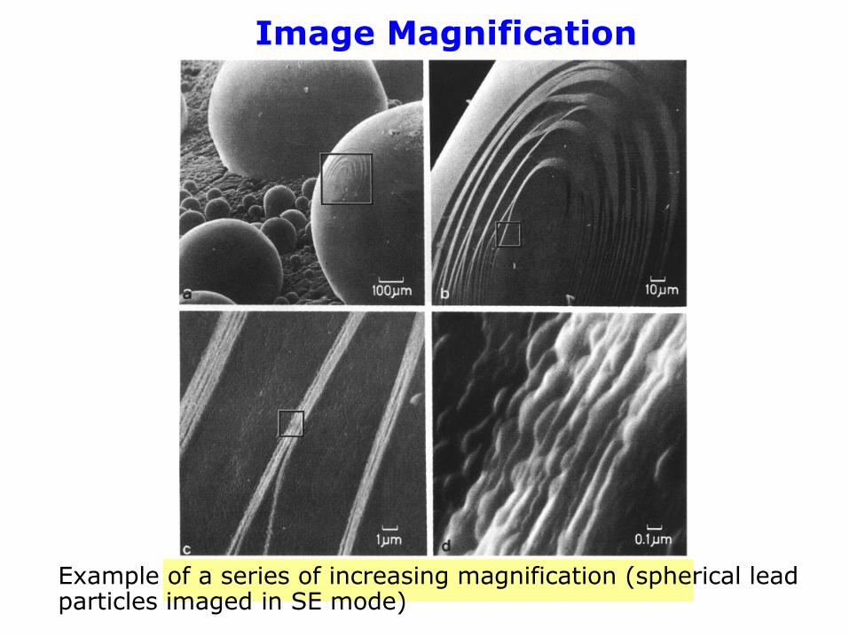
Image Magnification
Example of a series of increasing magnification (spherical lead particles imaged in SE mode)
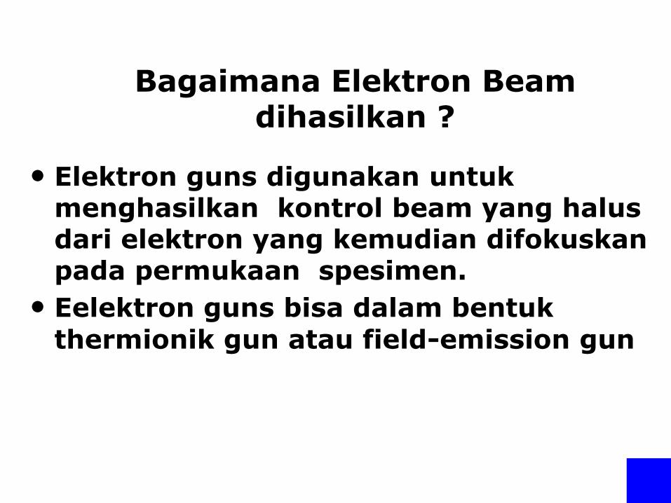
Bagaimana Elektron Beam dihasilkan ?
• Elektron guns digunakan untuk menghasilkan kontrol beam yang halus dari elektron yang kemudian difokuskan pada permukaan spesimen.
• Eelektron guns bisa dalam bentuk
thermionik gun atau field-emission gun
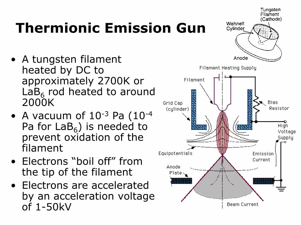
Thermionic Emission Gun
• A tungsten filament heated by DC to approximately 2700K or LaB6 rod heated to around 2000K
• A vacuum of 10-3 Pa (10-4
Pa for LaB6) is needed to prevent oxidation of the filament
• Electrons “boil off” from the tip of the filament
• Electrons are accelerated by an acceleration voltage of 1-50kV
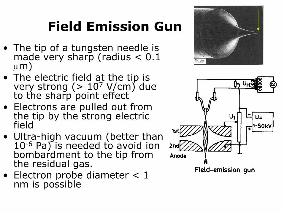
Field Emission Gun
• The tip of a tungsten needle is made very sharp (radius < 0.1 mm)
• The electric field at the tip is very strong (> 107 V/cm) due to the sharp point effect
• Electrons are pulled out from the tip by the strong electric field
• Ultra-high vacuum (better than 10-6 Pa) is needed to avoid ion bombardment to the tip from the residual gas.
• Electron probe diameter < 1 nm is possible
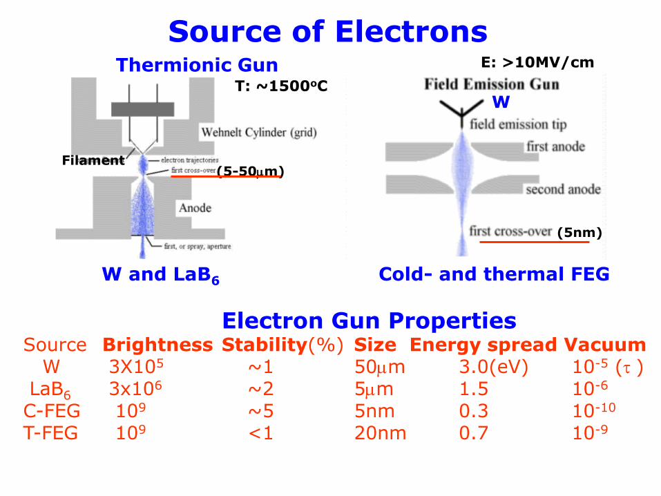
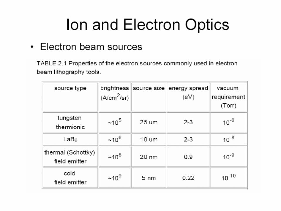
Source of Electrons
T: ~1500oC
Thermionic Gun
W and LaB6 Cold- and thermal FEG
Electron Gun PropertiesSource Brightness Stability(%) Size Energy spread Vacuum
W 3X10⁵ ~1 50mm 3.0(eV) 10-5 (t )LaB6 3x10⁶ ~2 5mm 1.5 10-6
C-FEG 109 ~5 5nm 0.3 10-10
T-FEG 109 <1 20nm 0.7 10-9
(5-50mm)
E: >10MV/cm
(5nm)
Filament
W
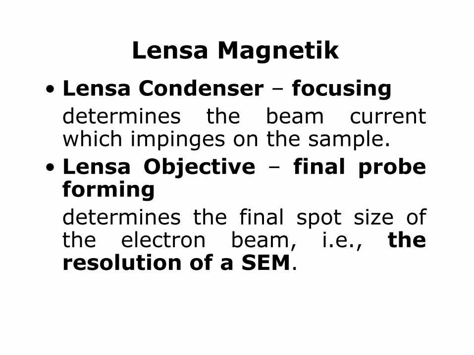
Lensa Magnetik
• Lensa Condenser – focusing
determines the beam currentwhich impinges on the sample.
• Lensa Objective – final probeforming
determines the final spot size ofthe electron beam, i.e., theresolution of a SEM.
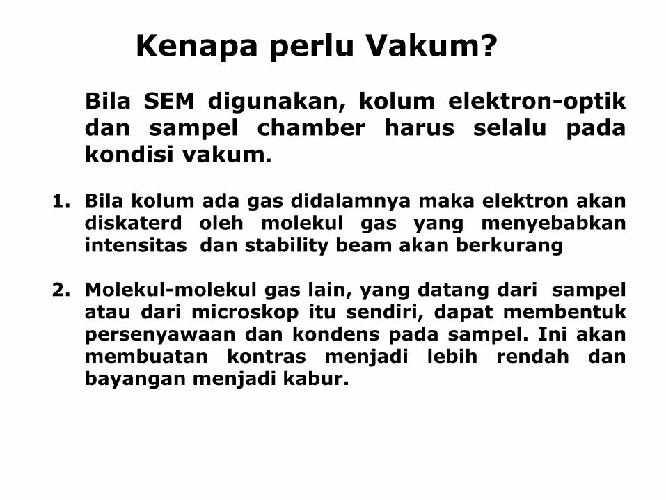
Kenapa perlu Vakum?
Bila SEM digunakan, kolum elektron-optikdan sampel chamber harus selalu padakondisi vakum.
1. Bila kolum ada gas didalamnya maka elektron akandiskaterd oleh molekul gas yang menyebabkanintensitas dan stability beam akan berkurang
2. Molekul-molekul gas lain, yang datang dari sampelatau dari microskop itu sendiri, dapat membentukpersenyawaan dan kondens pada sampel. Ini akanmembuatan kontras menjadi lebih rendah danbayangan menjadi kabur.
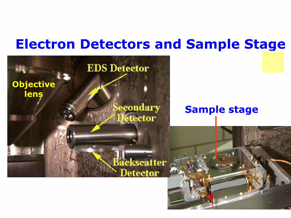
Electron Detectors and Sample Stage
Objectivelens
Sample stage
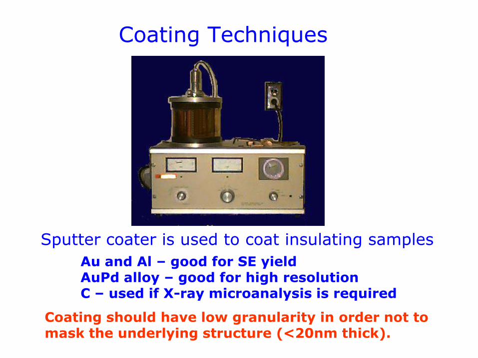
Coating Techniques
Sputter coater is used to coat insulating samples
Au and Al – good for SE yieldAuPd alloy – good for high resolutionC – used if X-ray microanalysis is required
Coating should have low granularity in order not to mask the underlying structure (<20nm thick).
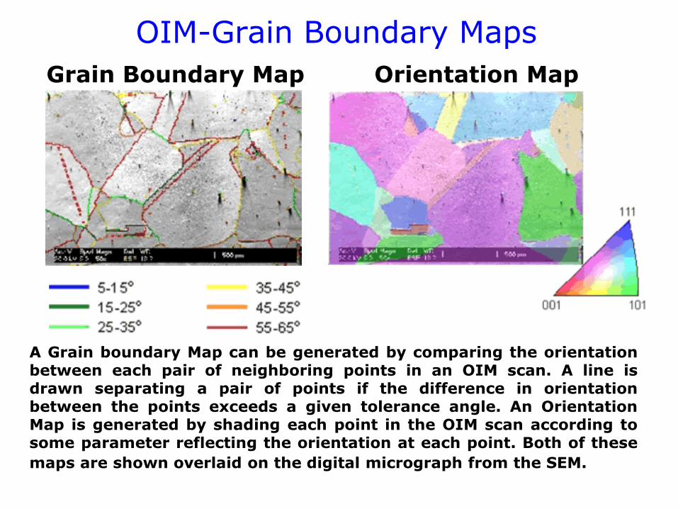
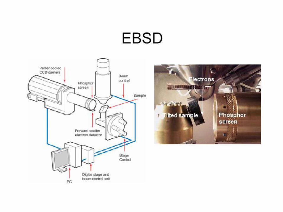
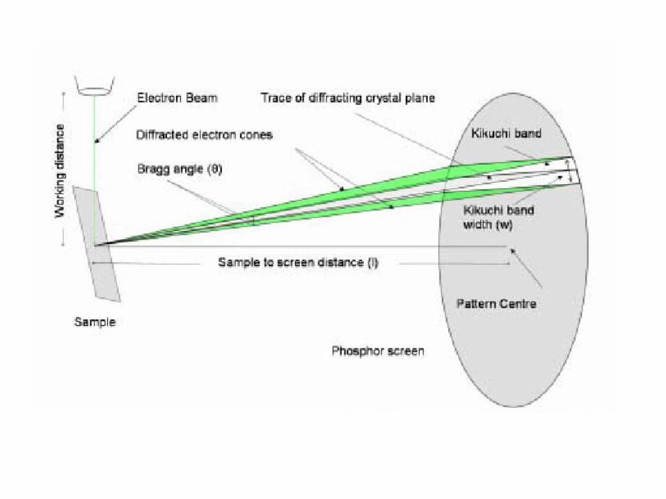
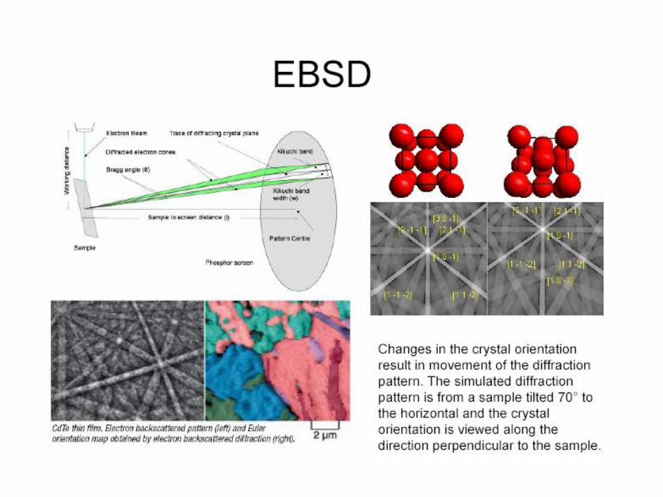
OIM-Grain Boundary Maps
Grain Boundary Map Orientation Map
A Grain boundary Map can be generated by comparing the orientationbetween each pair of neighboring points in an OIM scan. A line isdrawn separating a pair of points if the difference in orientationbetween the points exceeds a given tolerance angle. An OrientationMap is generated by shading each point in the OIM scan according tosome parameter reflecting the orientation at each point. Both of these
maps are shown overlaid on the digital micrograph from the SEM.