Embed Size (px)
Citation preview
S1
Electronic Supplementary Information
Biphenyl end-capped bithiazole co-oligomers for high performance
organic thin film field effect transistors
Kazuaki Oniwa,a Hiromasa Kikuchi,a Thangavel Kanagasekaran,a Hidekazu Shimotani,b Susumu Ikeda,a Naoki
Asao,a Yoshinori Yamamoto,a,c Katsumi Tanigakia,b and Tienan Jin*a
a WPI-Advanced Institute for Materials Research (WPI-AIMR), Tohoku University, Sendai 980-8577, Japan. Fax:
+81-22-217-5979; Tel: +81-22-217-6177; E-mail: [email protected]
b Graduate School of Science, Department of Physics, Sendai 980-8578, Tohoku University, Japan.
c State Key Laboratory of Fine Chemicals, Dalian University of Technology, Dalian 116012, China.
Electronic Supplementary Material (ESI) for ChemComm.This journal is © The Royal Society of Chemistry 2016

S2
General Information
The commercially available compounds and solvent were used as received. 1H NMR and 13C NMR spectra were
recorded on JEOL JNM AL 400 (400 MHz) spectrometers. 1H NMR spectra are reported as follows: chemical shift
in ppm δ relative to the chemical shift of CDCl3 at 7.26 ppm, integration, multiplicities (s = singlet, d = doublet, t =
triplet, q = quartet, m = multiplet, and br = broadened), and coupling constants (Hz). 13C NMR spectra were recorded
on JEOL JNM AL 400 (100.5 MHz) spectrometers with complete proton decoupling, and chemical shift reported in
ppm δ relative to the central line of triplet for CDCl3 at 77 ppm. Scanning electron microscope (SEM) observation
was carried out using a JEOL JSM-6500F instrument operated at an accelerating voltage of 30 kV. UV/Vis absorption
spectra were recorded on a JASCO V-650DS spectrometer. Fluorescence spectra were recorded on a HITACHI F-
7000 spectrophotometer and absolute fluorescence quantum yields were measured by a photon-counting method
using an integration sphere on a Hamamatsu Photonics C9920-02 spectrometer. Elemental analyses were measured
on J-SCIENCE Lab JM-10 and YANAKO YHS-11 in Central Analytical Facility, Institute of Multidisciplinary
Research for Advanced Materials, Tohoku University. DSC was measured by a RIGAKU DSC8230 using N2
atmosphere at a scan rate of 10 K/min. TGA was measured by a RIGAKU TAG8120. X-ray diffractions were
measured by RIGAKU Smart Lab 9SW using Cu-Kα radiation and zero dimensional mode Dte/X as high-speed
detector. The ionization potential (IP) was measured using the photoelectron spectrometer surface analyser (Riken
Keiki, AC-3E). Column chromatography was carried out employing silica gel 60 N (spherical, neutral, 40~100 μm,
KANTO Chemical Co.). Analytical thin-layer chromatography (TLC) was performed on 0.2 mm precoated plate
Kieselgel 60 F254 (Merck).
Synthesis of 2,2'-bithiazole
A mixture of 2-bromothiazole (32 mmol, 2.88 mL), Pd(OAc)2 (10 mol%, 718 mg), n-Bu4NBr (16 mmol, 5.16 g), and
diisopropylethylamine (32 mmol, 5.57 mL) in toluene (12 mL) was stirred for 18 h at 105 °C. The resulting mixture
was poured into water and extracted by CHCl3. After concentration, the residue was purified by silica gel
chromatography, giving the corresponding 2,2'-bithiazole in 90% (2.43 g) yield as a yellow solid. 1H NMR (400 MHz,
CDCl3): δ 7.90 (d, 2H, J = 2.8 Hz), 7.45 (d, 2H, J = 2.8 Hz); 13C NMR (100 MHz, CDCl3): δ 161.54, 143.80, 120.87.
Synthesis of 5,5'-dibromo-2,2'-bithiazole
A mixture of 2,2'-bithiazole (6 mmol, 1.01 g) and NBS (24 mmol, 4.27 g) in DMF (30 mL) was stirred for 12 h at
60 °C. The resulting mixture was poured into water and extracted by CHCl3. After concentration, the residue was
purified by recrystallization using MeOH and CHCl3, giving the corresponding 5,5'-dibromo-2,2'-bithiazole in 95%
(1.85 g) yield as a white solid. 1H NMR (400 MHz, CDCl3): δ 7.75 (s, 2H); 13C NMR (100 MHz, CDCl3): δ 161.79,
145.06, 111.95.
Synthesis of 5,5'-di([1,1'-biphenyl]-4-yl)-2,2'-bithiazole [BP2Tz(in)]
A mixture of 5,5'-dibromo-2,2'-bithiazole (2.5 mmol, 815 mg), [1,1'-biphenyl]-4-ylboronic acid (6.25 mmol, 1.24 g),
K3PO4・nH2O (2.8 g), Pd2(dba)3・CHCl3 (5 mol%, 129 mg), and X-phos (20 mol%, 238 mg) in DMF (18 mL) was
stirred at 120 °C for 18 h. The mixture was filtered and the resulting residue was washed by water, MeOH, and CHCl3.
S3
After sublimation at 330 °C under high vacuum, BP2Tz(in) was obtained as a yellow solid in 40% (470 mg) yield.
Anal. calcd for C30H20N2S2: C 76.24, H 4.27, N 5.93, S 13.57; found: C 75.97, H 4.34, N 5.70, S 13.15%.
Synthesis of 2-([1,1'-biphenyl]-4-yl)thiazole
[1,1'-biphenyl]-4-ylboronic acid (12.2 mmol, 2.42 g), K3PO4・nH2O (6 g), and Pd(PPh3)4 were dissolved in DMF
(20 mL) under nitrogen atmosphere. Then 2-bromothiazole (10.0 mmol, 0.902 mL) was added. The mixture was
stirred for overnight at 100 °C. The resulting mixture was poured into water and extracted by CHCl3. After
concentration, the residue was purified by silica gel chromatography, giving the corresponding 2-biphenylthiazole in
70% (1.66 g) yield as a white solid. 1H NMR (400 MHz, CDCl3): δ 8.06 (d, 2H. J = 8.0 Hz), 7.90 (d, 1H, J = 2.8 Hz),
7.69 (d, 2H, J = 8.0 Hz), 7.64 (d, 2H, J = 8.0 Hz), 7.40 (t, 2H, J = 8.0 Hz), 7.38 (t, 1H, J = 8.0 Hz), 7.36 (d, 1H, J =
2.8 Hz); 13C NMR (100 MHz, CDCl3): δ 167.99, 143.60, 142.71, 140.11, 132.39, 128.82, 127.71, 127.55, 126.96,
118.72.
Synthesis of 2,2'-di([1,1'-biphenyl]-4-yl)-5,5'-bithiazole [BP2Tz(out)]
To a solution of 2-([1,1'-biphenyl]-4-yl)thiazole (2.1 mmol, 577 mg) in anhydrous THF (6 mL) was added bis(2,2,6,6-
tetramethylpiperidine) zinc lithium magnesium chloride complex (3.3 mL of a 0.35 M solution in THF) dropwise
over 30 min at rt. The reaction mixture was stirred at room temperature for 1 h and then cooled to -40 °C. Chloranil
(2.51 mmol, 616 mg) was added portion-wise over 30 min. The reaction mixture was slowly warmed to 0 °C. The
mixture was quenched with sat. NH4Cl solution (3 mL) and filtered. The resulting residue was washed by water,
MeOH, and CHCl3. After sublimation at 325 °C, BP2Tz(out) was obtained as a yellow solid in 72% (340 mg) yield.
Anal. calcd for C30H20N2S2: C 76.24, H 4.27, N 5.93, S 13.57; found: C 76.24, H 4.36, N 5.92, S 13.29%
S4
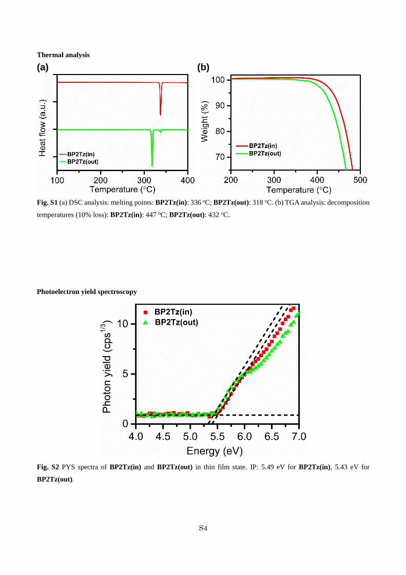
Thermal analysis
(a) (b)
Fig. S1 (a) DSC analysis: melting points: BP2Tz(in): 336 oC; BP2Tz(out): 318 oC. (b) TGA analysis: decomposition
temperatures (10% loss): BP2Tz(in): 447 oC; BP2Tz(out): 432 oC.
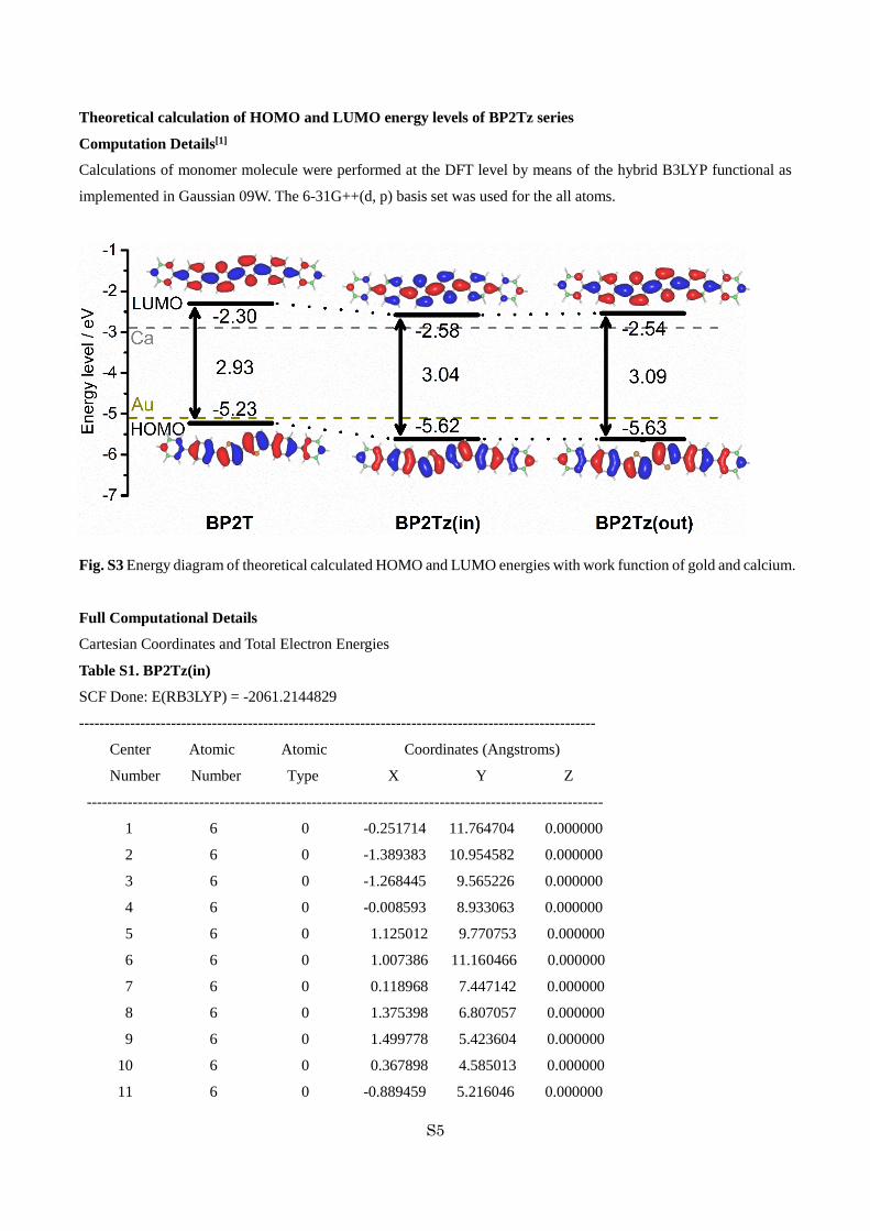
Photoelectron yield spectroscopy
Fig. S2 PYS spectra of BP2Tz(in) and BP2Tz(out) in thin film state. IP: 5.49 eV for BP2Tz(in), 5.43 eV for
BP2Tz(out).
S5
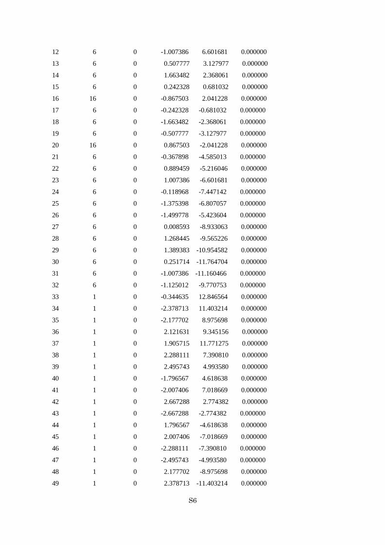
Theoretical calculation of HOMO and LUMO energy levels of BP2Tz series
Computation Details[1]
Calculations of monomer molecule were performed at the DFT level by means of the hybrid B3LYP functional as
implemented in Gaussian 09W. The 6-31G++(d, p) basis set was used for the all atoms.
Fig. S3 Energy diagram of theoretical calculated HOMO and LUMO energies with work function of gold and calcium.
Full Computational Details
Cartesian Coordinates and Total Electron Energies
Table S1. BP2Tz(in)
SCF Done: E(RB3LYP) = -2061.2144829
-----------------------------------------------------------------------------------------------------
Center Atomic Atomic Coordinates (Angstroms)
Number Number Type X Y Z
-----------------------------------------------------------------------------------------------------
1 6 0 -0.251714 11.764704 0.000000
2 6 0 -1.389383 10.954582 0.000000
3 6 0 -1.268445 9.565226 0.000000
4 6 0 -0.008593 8.933063 0.000000
5 6 0 1.125012 9.770753 0.000000
6 6 0 1.007386 11.160466 0.000000
7 6 0 0.118968 7.447142 0.000000
8 6 0 1.375398 6.807057 0.000000
9 6 0 1.499778 5.423604 0.000000
10 6 0 0.367898 4.585013 0.000000
11 6 0 -0.889459 5.216046 0.000000
S6
12 6 0 -1.007386 6.601681 0.000000
13 6 0 0.507777 3.127977 0.000000
14 6 0 1.663482 2.368061 0.000000
15 6 0 0.242328 0.681032 0.000000
16 16 0 -0.867503 2.041228 0.000000
17 6 0 -0.242328 -0.681032 0.000000
18 6 0 -1.663482 -2.368061 0.000000
19 6 0 -0.507777 -3.127977 0.000000
20 16 0 0.867503 -2.041228 0.000000
21 6 0 -0.367898 -4.585013 0.000000
22 6 0 0.889459 -5.216046 0.000000
23 6 0 1.007386 -6.601681 0.000000
24 6 0 -0.118968 -7.447142 0.000000
25 6 0 -1.375398 -6.807057 0.000000
26 6 0 -1.499778 -5.423604 0.000000
27 6 0 0.008593 -8.933063 0.000000
28 6 0 1.268445 -9.565226 0.000000
29 6 0 1.389383 -10.954582 0.000000
30 6 0 0.251714 -11.764704 0.000000
31 6 0 -1.007386 -11.160466 0.000000
32 6 0 -1.125012 -9.770753 0.000000
33 1 0 -0.344635 12.846564 0.000000
34 1 0 -2.378713 11.403214 0.000000
35 1 0 -2.177702 8.975698 0.000000
36 1 0 2.121631 9.345156 0.000000
37 1 0 1.905715 11.771275 0.000000
38 1 0 2.288111 7.390810 0.000000
39 1 0 2.495743 4.993580 0.000000
40 1 0 -1.796567 4.618638 0.000000
41 1 0 -2.007406 7.018669 0.000000
42 1 0 2.667288 2.774382 0.000000
43 1 0 -2.667288 -2.774382 0.000000
44 1 0 1.796567 -4.618638 0.000000
45 1 0 2.007406 -7.018669 0.000000
46 1 0 -2.288111 -7.390810 0.000000
47 1 0 -2.495743 -4.993580 0.000000
48 1 0 2.177702 -8.975698 0.000000
49 1 0 2.378713 -11.403214 0.000000
S7
50 1 0 0.344635 -12.846564 0.000000
51 1 0 -1.905715 -11.771275 0.000000
52 1 0 -2.121631 -9.345156 0.000000
53 7 0 1.512251 1.013883 0.000000
54 7 0 -1.512251 -1.013883 0.000000
-----------------------------------------------------------------------------------------------------
Table S2. BP2Tz(out)
SCF Done: E(RB3LYP) = -2061.2163087
------------------------------------------------------------------------------------------------------
Center Atomic Atomic Coordinates (Angstroms)
Number Number Type X Y Z
------------------------------------------------------------------------------------------------------
1 6 0 -0.236002 11.772640 0.000000
2 6 0 -1.377853 10.968457 0.000000
3 6 0 -1.263874 9.578529 0.000000
4 6 0 -0.007189 8.939968 0.000000
5 6 0 1.130715 9.771878 0.000000
6 6 0 1.020064 11.162112 0.000000
7 6 0 0.113681 7.453107 0.000000
8 6 0 1.369066 6.809145 0.000000
9 6 0 1.488693 5.425535 0.000000
10 6 0 0.347246 4.603205 0.000000
11 6 0 -0.909852 5.229722 0.000000
12 6 0 -1.020064 6.615768 0.000000
13 6 0 0.505124 3.148530 0.000000
14 6 0 1.518579 1.175928 0.000000
15 6 0 0.228000 0.685073 0.000000
16 16 0 -0.878868 2.043826 0.000000
17 6 0 -0.228000 -0.685073 0.000000
18 6 0 -1.518579 -1.175928 0.000000
19 6 0 -0.505124 -3.148530 0.000000
20 16 0 0.878868 -2.043826 0.000000
21 6 0 -0.347246 -4.603205 0.000000
22 6 0 0.909852 -5.229722 0.000000
23 6 0 1.020064 -6.615768 0.000000
24 6 0 -0.113681 -7.453107 0.000000
25 6 0 -1.369066 -6.809145 0.000000
S8
26 6 0 -1.488693 -5.425535 0.000000
27 6 0 0.007189 -8.939968 0.000000
28 6 0 1.263874 -9.578529 0.000000
29 6 0 1.377853 -10.968457 0.000000
30 6 0 0.236002 -11.772640 0.000000
31 6 0 -1.020064 -11.162112 0.000000
32 6 0 -1.130715 -9.771878 0.000000
33 1 0 -0.323444 12.854966 0.000000
34 1 0 -2.364856 11.422166 0.000000
35 1 0 -2.176242 8.993922 0.000000
36 1 0 2.125005 9.341166 0.000000
37 1 0 1.921444 11.768357 0.000000
38 1 0 2.282943 7.390920 0.000000
39 1 0 2.468372 4.960887 0.000000
40 1 0 -1.819001 4.634698 0.000000
41 1 0 -2.016739 7.040255 0.000000
42 1 0 2.406245 0.553514 0.000000
43 1 0 -2.406245 -0.553514 0.000000
44 1 0 1.819001 -4.634698 0.000000
45 1 0 2.016739 -7.040255 0.000000
46 1 0 -2.282943 -7.390920 0.000000
47 1 0 -2.468372 -4.960887 0.000000
48 1 0 2.176242 -8.993922 0.000000
49 1 0 2.364856 -11.422166 0.000000
50 1 0 0.323444 -12.854966 0.000000
51 1 0 -1.921444 -11.768357 0.000000
52 1 0 -2.125005 -9.341166 0.000000
53 7 0 -1.662023 -2.531124 0.000000
54 7 0 1.662023 2.531124 0.000000
------------------------------------------------------------------------------------------------------
S9
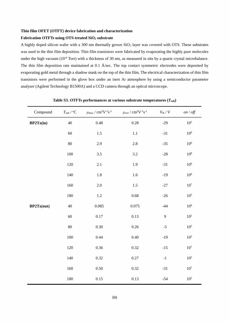
Thin film OFET (OTFT) device fabrication and characterization
Fabrication OTFTs using OTS-treated SiO2 substrate
A highly doped silicon wafer with a 300 nm thermally grown SiO2 layer was covered with OTS. These substrates
was used in the thin film deposition. Thin film transistors were fabricated by evaporating the highly pure molecules
under the high vacuum (10-6 Torr) with a thickness of 30 nm, as measured in situ by a quartz crystal microbalance.
The thin film deposition rate maintained at 0.1 Å/sec. The top contact symmetric electrodes were deposited by
evaporating gold metal through a shadow mask on the top of the thin film. The electrical characterization of thin film
transistors were performed in the glove box under an inert Ar atmosphere by using a semiconductor parameter
analyzer (Agilent Technology B1500A) and a CCD camera through an optical microscope.
Table S3. OTFTs performances at various substrate temperatures (Tsub)
Compound Tsub / oC μmax / cm2V-1s-1 μave / cm2V-1s-1 Vth / V on / off
BP2Tz(in) 40 0.48 0.28 -29 105
60 1.5 1.1 -31 106
80 2.9 2.8 -35 106
100 3.5 3.2 -28 108
120 2.1 1.9 -31 106
140 1.8 1.6 -19 106
160 2.0 1.5 -27 107
180 1.2 0.68 -26 105
BP2Tz(out) 40 0.085 0.075 -44 104
60 0.17 0.13 9 105
80 0.30 0.26 -5 105
100 0.44 0.40 -19 105
120 0.36 0.32 -15 107
140 0.32 0.27 -1 105
160 0.50 0.32 -31 107
180 0.15 0.13 -54 105
S10
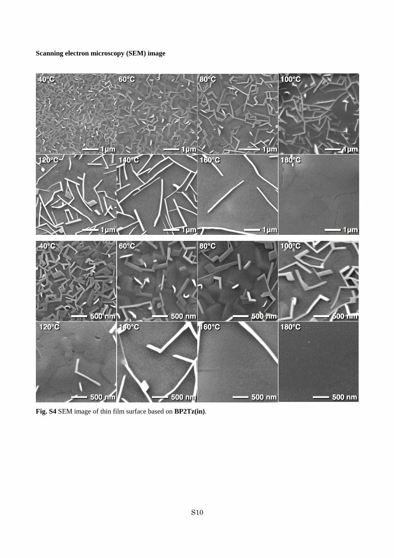
Scanning electron microscopy (SEM) image
Fig. S4 SEM image of thin film surface based on BP2Tz(in).
S11
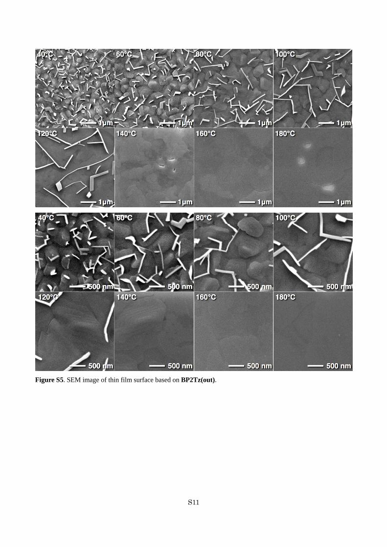
Figure S5. SEM image of thin film surface based on BP2Tz(out).
S12
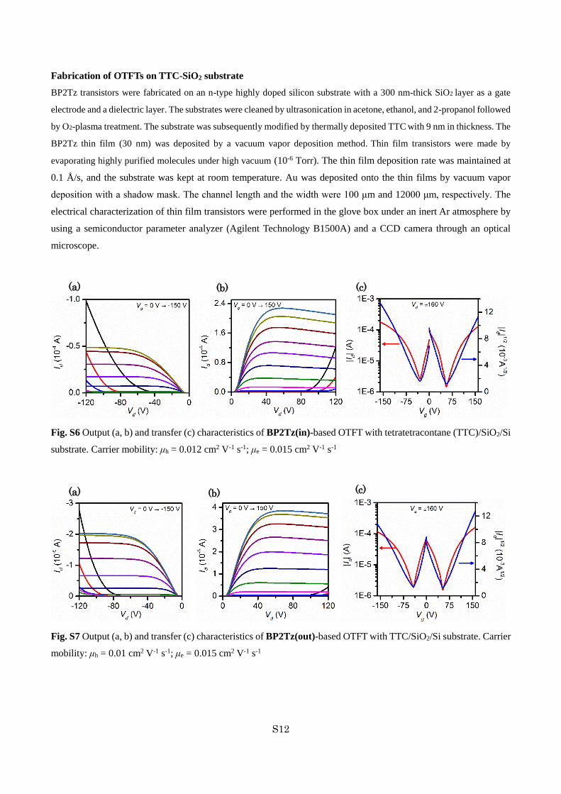
Fabrication of OTFTs on TTC-SiO2 substrate
BP2Tz transistors were fabricated on an n-type highly doped silicon substrate with a 300 nm-thick SiO2 layer as a gate
electrode and a dielectric layer. The substrates were cleaned by ultrasonication in acetone, ethanol, and 2-propanol followed
by O2-plasma treatment. The substrate was subsequently modified by thermally deposited TTC with 9 nm in thickness. The
BP2Tz thin film (30 nm) was deposited by a vacuum vapor deposition method. Thin film transistors were made by
evaporating highly purified molecules under high vacuum (10-6 Torr). The thin film deposition rate was maintained at
0.1 Å/s, and the substrate was kept at room temperature. Au was deposited onto the thin films by vacuum vapor
deposition with a shadow mask. The channel length and the width were 100 μm and 12000 μm, respectively. The
electrical characterization of thin film transistors were performed in the glove box under an inert Ar atmosphere by
using a semiconductor parameter analyzer (Agilent Technology B1500A) and a CCD camera through an optical
microscope.
Fig. S6 Output (a, b) and transfer (c) characteristics of BP2Tz(in)-based OTFT with tetratetracontane (TTC)/SiO2/Si
substrate. Carrier mobility: μh = 0.012 cm2 V-1 s-1; μe = 0.015 cm2 V-1 s-1
Fig. S7 Output (a, b) and transfer (c) characteristics of BP2Tz(out)-based OTFT with TTC/SiO2/Si substrate. Carrier
mobility: μh = 0.01 cm2 V-1 s-1; μe = 0.015 cm2 V-1 s-1
(a) (b) (c)
(a) (b) (c)
S13
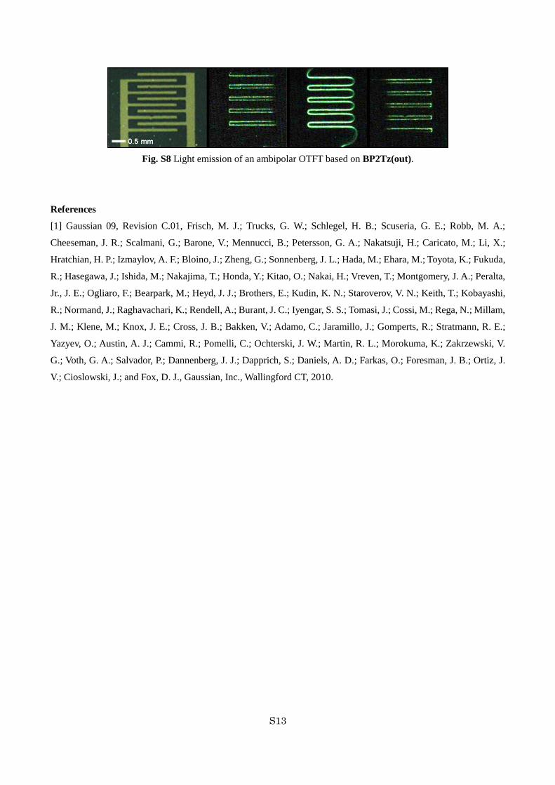
Fig. S8 Light emission of an ambipolar OTFT based on BP2Tz(out).
References
[1] Gaussian 09, Revision C.01, Frisch, M. J.; Trucks, G. W.; Schlegel, H. B.; Scuseria, G. E.; Robb, M. A.;
Cheeseman, J. R.; Scalmani, G.; Barone, V.; Mennucci, B.; Petersson, G. A.; Nakatsuji, H.; Caricato, M.; Li, X.;
Hratchian, H. P.; Izmaylov, A. F.; Bloino, J.; Zheng, G.; Sonnenberg, J. L.; Hada, M.; Ehara, M.; Toyota, K.; Fukuda,
R.; Hasegawa, J.; Ishida, M.; Nakajima, T.; Honda, Y.; Kitao, O.; Nakai, H.; Vreven, T.; Montgomery, J. A.; Peralta,
Jr., J. E.; Ogliaro, F.; Bearpark, M.; Heyd, J. J.; Brothers, E.; Kudin, K. N.; Staroverov, V. N.; Keith, T.; Kobayashi,
R.; Normand, J.; Raghavachari, K.; Rendell, A.; Burant, J. C.; Iyengar, S. S.; Tomasi, J.; Cossi, M.; Rega, N.; Millam,
J. M.; Klene, M.; Knox, J. E.; Cross, J. B.; Bakken, V.; Adamo, C.; Jaramillo, J.; Gomperts, R.; Stratmann, R. E.;
Yazyev, O.; Austin, A. J.; Cammi, R.; Pomelli, C.; Ochterski, J. W.; Martin, R. L.; Morokuma, K.; Zakrzewski, V.
G.; Voth, G. A.; Salvador, P.; Dannenberg, J. J.; Dapprich, S.; Daniels, A. D.; Farkas, O.; Foresman, J. B.; Ortiz, J.
V.; Cioslowski, J.; and Fox, D. J., Gaussian, Inc., Wallingford CT, 2010.