Embed Size (px)
Citation preview
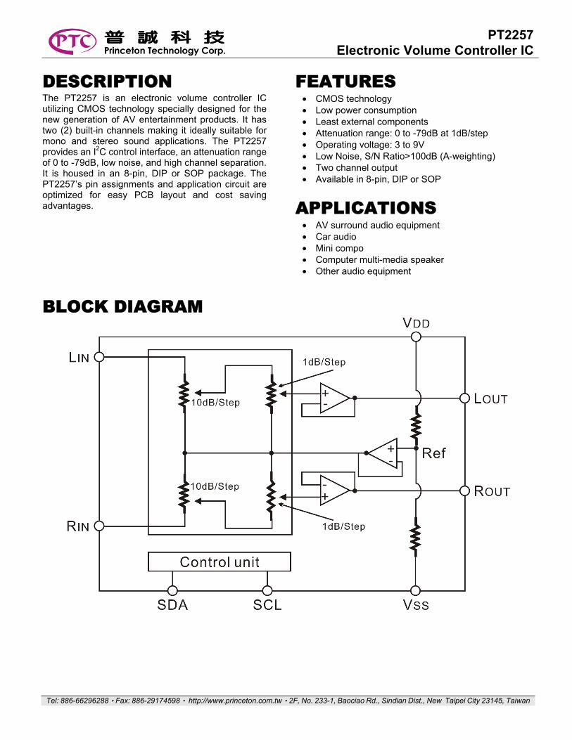
PT2257Electronic Volume Controller IC
Tel: 886-66296288‧Fax: 886-29174598‧ http://www.princeton.com.tw‧2F, No. 233-1, Baociao Rd., Sindian Dist., New Taipei City 23145, Taiwan
DESCRIPTION The PT2257 is an electronic volume controller IC utilizing CMOS technology specially designed for the new generation of AV entertainment products. It has two (2) built-in channels making it ideally suitable for mono and stereo sound applications. The PT2257 provides an I2C control interface, an attenuation range of 0 to -79dB, low noise, and high channel separation. It is housed in an 8-pin, DIP or SOP package. The PT2257’s pin assignments and application circuit are optimized for easy PCB layout and cost saving advantages.
FEATURES • CMOS technology • Low power consumption • Least external components • Attenuation range: 0 to -79dB at 1dB/step • Operating voltage: 3 to 9V • Low Noise, S/N Ratio>100dB (A-weighting) • Two channel output • Available in 8-pin, DIP or SOP
APPLICATIONS • AV surround audio equipment • Car audio • Mini compo • Computer multi-media speaker • Other audio equipment
BLOCK DIAGRAM
PT2257
V1.5 2 March 2013
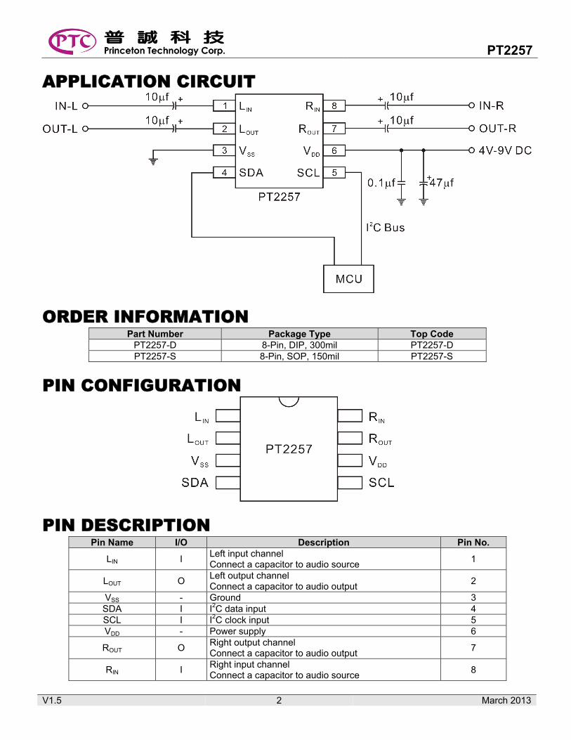
APPLICATION CIRCUIT
ORDER INFORMATION Part Number Package Type Top Code
PT2257-D 8-Pin, DIP, 300mil PT2257-D PT2257-S 8-Pin, SOP, 150mil PT2257-S
PIN CONFIGURATION
PIN DESCRIPTION Pin Name I/O Description Pin No.
LIN I Left input channel Connect a capacitor to audio source
1
LOUT O Left output channel Connect a capacitor to audio output
2
VSS - Ground 3 SDA I I2C data input 4 SCL I I2C clock input 5 VDD - Power supply 6
ROUT O Right output channel Connect a capacitor to audio output
7
RIN I Right input channel Connect a capacitor to audio source
8
PT2257
V1.5 3 March 2013
FUNCTION DESCRIPTION BUS INTERFACE Data are transmitted to and from the microprocessor to the PT2257 via the SDA and SCL. The SDA and SCL make up the BUS Interface. It should be noted that the pull-up resistors must be connected to the positive supply voltage.
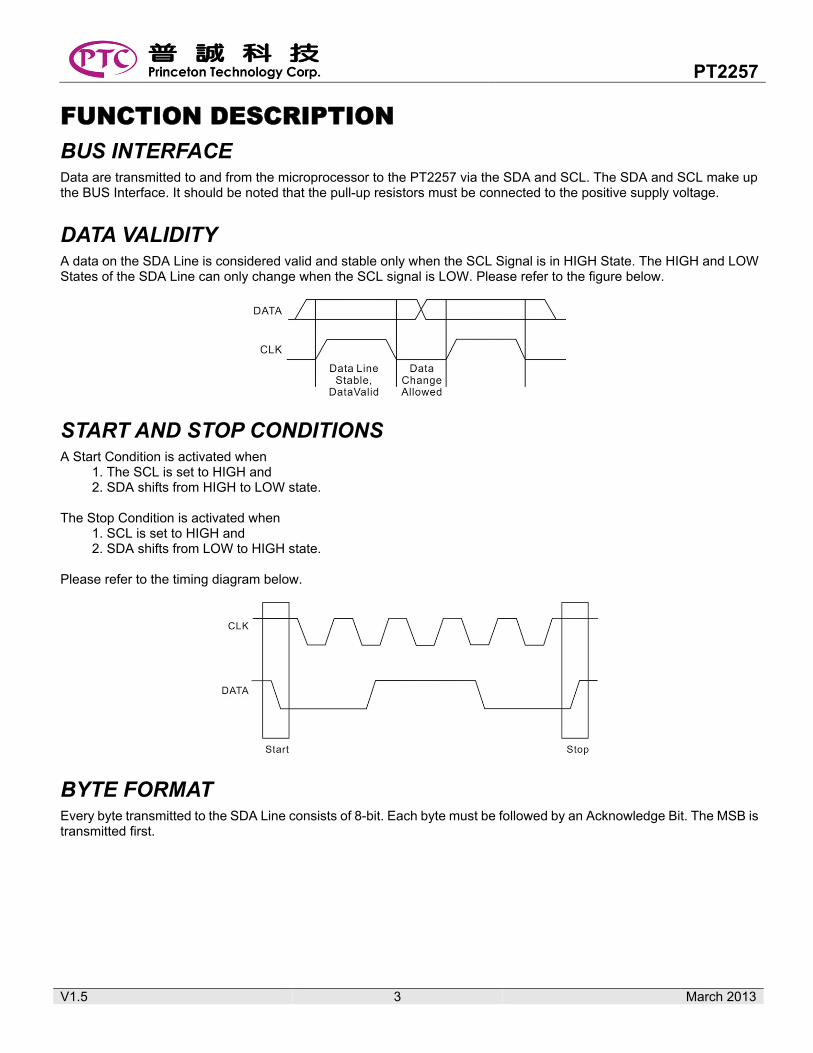
DATA VALIDITY A data on the SDA Line is considered valid and stable only when the SCL Signal is in HIGH State. The HIGH and LOW States of the SDA Line can only change when the SCL signal is LOW. Please refer to the figure below.
START AND STOP CONDITIONS A Start Condition is activated when
1. The SCL is set to HIGH and 2. SDA shifts from HIGH to LOW state.
The Stop Condition is activated when
1. SCL is set to HIGH and 2. SDA shifts from LOW to HIGH state.
Please refer to the timing diagram below.
BYTE FORMAT Every byte transmitted to the SDA Line consists of 8-bit. Each byte must be followed by an Acknowledge Bit. The MSB is transmitted first.
PT2257
V1.5 4 March 2013
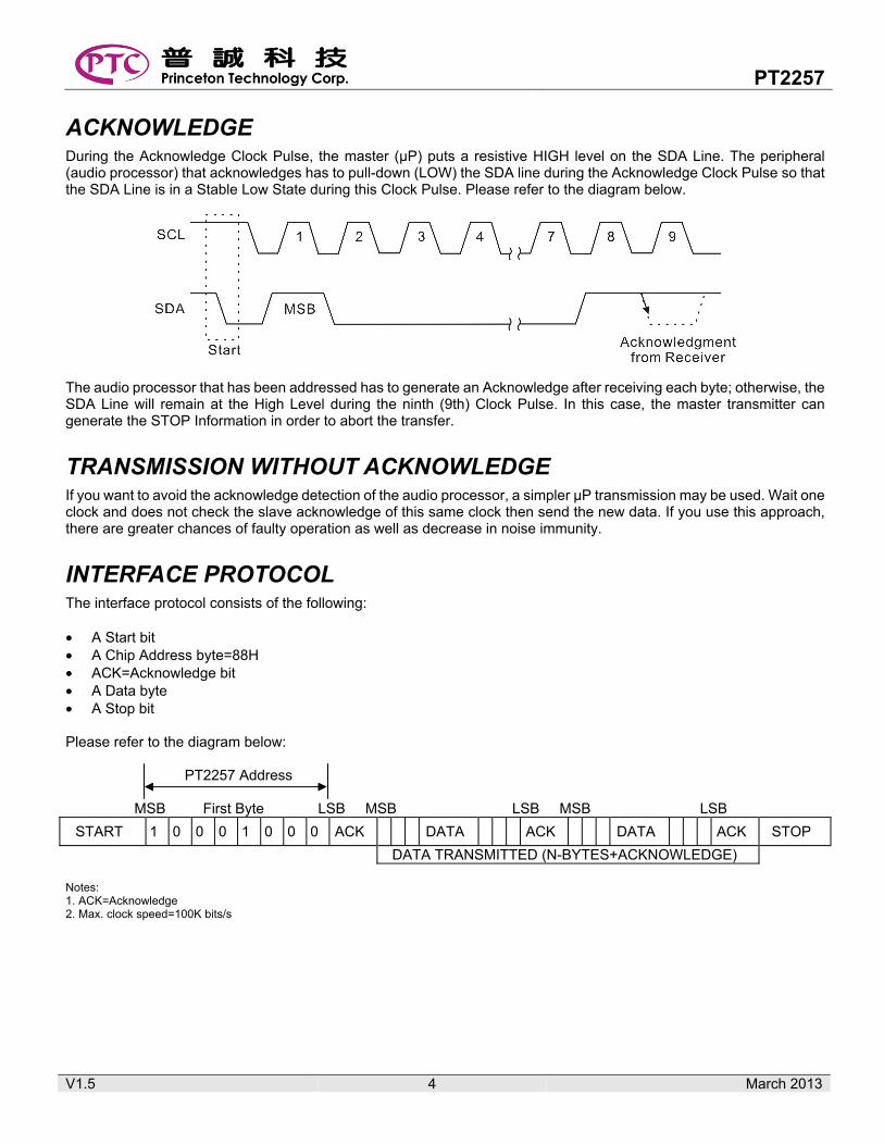
ACKNOWLEDGE During the Acknowledge Clock Pulse, the master (µP) puts a resistive HIGH level on the SDA Line. The peripheral (audio processor) that acknowledges has to pull-down (LOW) the SDA line during the Acknowledge Clock Pulse so that the SDA Line is in a Stable Low State during this Clock Pulse. Please refer to the diagram below.
The audio processor that has been addressed has to generate an Acknowledge after receiving each byte; otherwise, the SDA Line will remain at the High Level during the ninth (9th) Clock Pulse. In this case, the master transmitter can generate the STOP Information in order to abort the transfer.
TRANSMISSION WITHOUT ACKNOWLEDGE If you want to avoid the acknowledge detection of the audio processor, a simpler µP transmission may be used. Wait one clock and does not check the slave acknowledge of this same clock then send the new data. If you use this approach, there are greater chances of faulty operation as well as decrease in noise immunity.
INTERFACE PROTOCOL The interface protocol consists of the following: • A Start bit • A Chip Address byte=88H • ACK=Acknowledge bit • A Data byte • A Stop bit Please refer to the diagram below: PT2257 Address MSB First Byte LSB MSB LSB MSB LSB
START 1 0 0 0 1 0 0 0 ACK DATA ACK DATA ACK STOP
DATA TRANSMITTED (N-BYTES+ACKNOWLEDGE) Notes: 1. ACK=Acknowledge 2. Max. clock speed=100K bits/s
PT2257
V1.5 5 March 2013
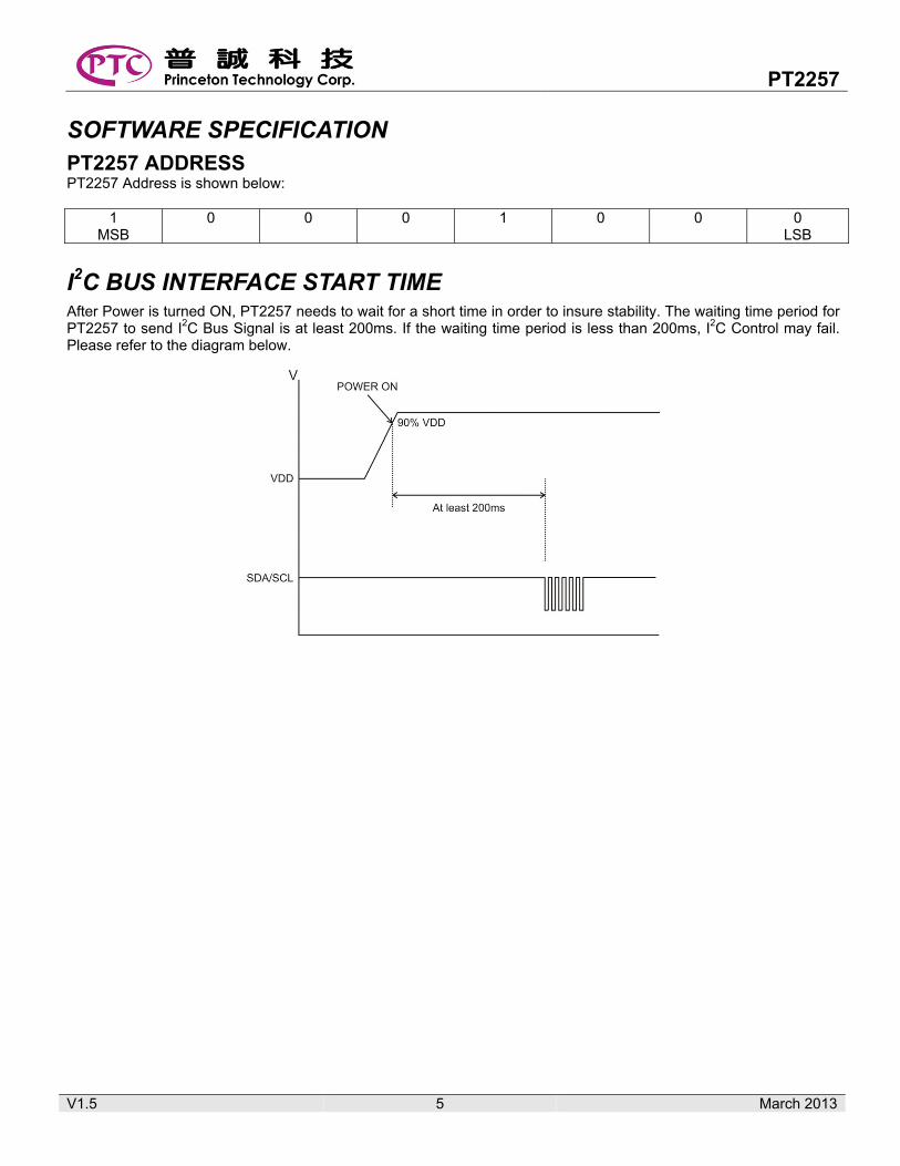
SOFTWARE SPECIFICATION PT2257 ADDRESS PT2257 Address is shown below:
1 MSB
0 0 0 1 0 0 0 LSB
I2C BUS INTERFACE START TIME After Power is turned ON, PT2257 needs to wait for a short time in order to insure stability. The waiting time period for PT2257 to send I2C Bus Signal is at least 200ms. If the waiting time period is less than 200ms, I2C Control may fail. Please refer to the diagram below.
PT2257
V1.5 6 March 2013
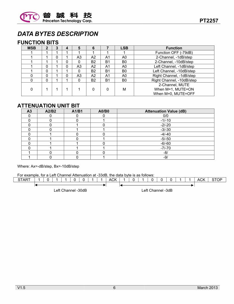
DATA BYTES DESCRIPTION FUNCTION BITS
MSB 2 3 4 5 6 7 LSB Function 1 1 1 1 1 1 1 1 Function OFF (-79dB) 1 1 0 1 A3 A2 A1 A0 2-Channel, -1dB/step 1 1 1 0 0 B2 B1 B0 2-Channel, -10dB/step 1 0 1 0 A3 A2 A1 A0 Left Channel, -1dB/step 1 0 1 1 0 B2 B1 B0 Left Channel, -10dB/step 0 0 1 0 A3 A2 A1 A0 Right Channel, -1dB/step 0 0 1 1 0 B2 B1 B0 Right Channel, -10dB/step
0 1 1 1 1 0 0 M 2-Channel, MUTE
When M=1, MUTE=ON When M=0, MUTE=OFF
ATTENUATION UNIT BIT
A3 A2/B2 A1/B1 A0/B0 Attenuation Value (dB) 0 0 0 0 0/0 0 0 0 1 -1/-10 0 0 1 0 -2/-20 0 0 1 1 -3/-30 0 1 0 0 -4/-40 0 1 0 1 -5/-50 0 1 1 0 -6/-60 0 1 1 1 -7/-70 1 0 0 0 -8/ 1 0 0 1 -9/
Where: Ax=-dB/step, Bx=-10dB/step For example, for a Left Channel Attenuation at -33dB, the data byte is as follows: START 1 0 1 1 0 0 1 1 ACK 1 0 1 0 0 0 1 1 ACK STOP
Left Channel -30dB Left Channel -3dB
PT2257
V1.5 7 March 2013
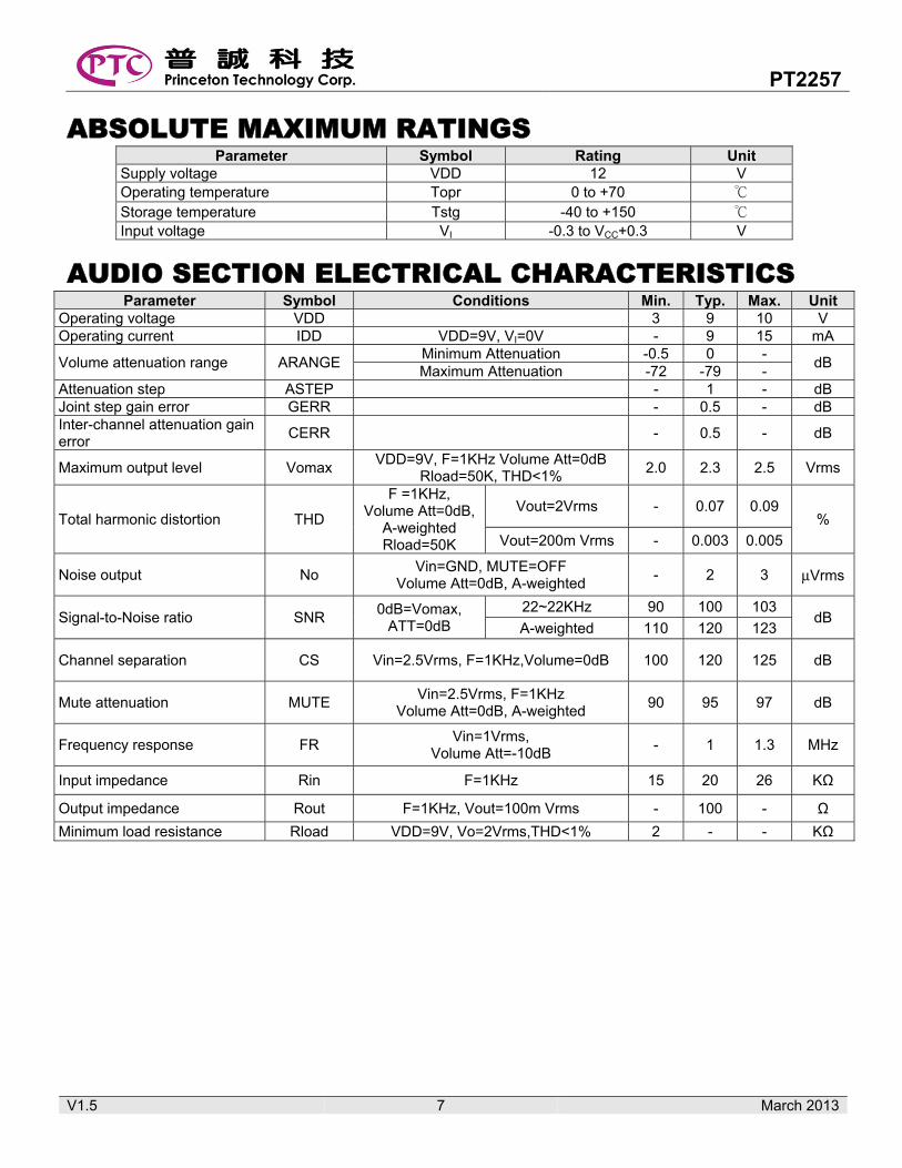
ABSOLUTE MAXIMUM RATINGS Parameter Symbol Rating Unit
Supply voltage VDD 12 V Operating temperature Topr 0 to +70
Storage temperature Tstg -40 to +150 Input voltage VI -0.3 to VCC+0.3 V
AUDIO SECTION ELECTRICAL CHARACTERISTICS Parameter Symbol Conditions Min. Typ. Max. Unit
Operating voltage VDD 3 9 10 V Operating current IDD VDD=9V, VI=0V - 9 15 mA
Volume attenuation range ARANGE Minimum Attenuation -0.5 0 -
dB Maximum Attenuation -72 -79 -
Attenuation step ASTEP - 1 - dB Joint step gain error GERR - 0.5 - dB Inter-channel attenuation gain error
CERR - 0.5 - dB
Maximum output level Vomax VDD=9V, F=1KHz Volume Att=0dB
Rload=50K, THD<1% 2.0 2.3 2.5 Vrms
Total harmonic distortion THD
F =1KHz, Volume Att=0dB,
A-weighted Rload=50K
Vout=2Vrms - 0.07 0.09%
Vout=200m Vrms - 0.003 0.005
Noise output No Vin=GND, MUTE=OFF
Volume Att=0dB, A-weighted - 2 3 μVrms
Signal-to-Noise ratio SNR 0dB=Vomax,
ATT=0dB 22~22KHz 90 100 103
dB A-weighted 110 120 123
Channel separation CS Vin=2.5Vrms, F=1KHz,Volume=0dB 100 120 125 dB
Mute attenuation MUTE Vin=2.5Vrms, F=1KHz
Volume Att=0dB, A-weighted 90 95 97 dB
Frequency response FR Vin=1Vrms,
Volume Att=-10dB - 1 1.3 MHz
Input impedance Rin F=1KHz 15 20 26 KΩ
Output impedance Rout F=1KHz, Vout=100m Vrms - 100 - Ω
Minimum load resistance Rload VDD=9V, Vo=2Vrms,THD<1% 2 - - KΩ
PT2257
V1.5 8 March 2013
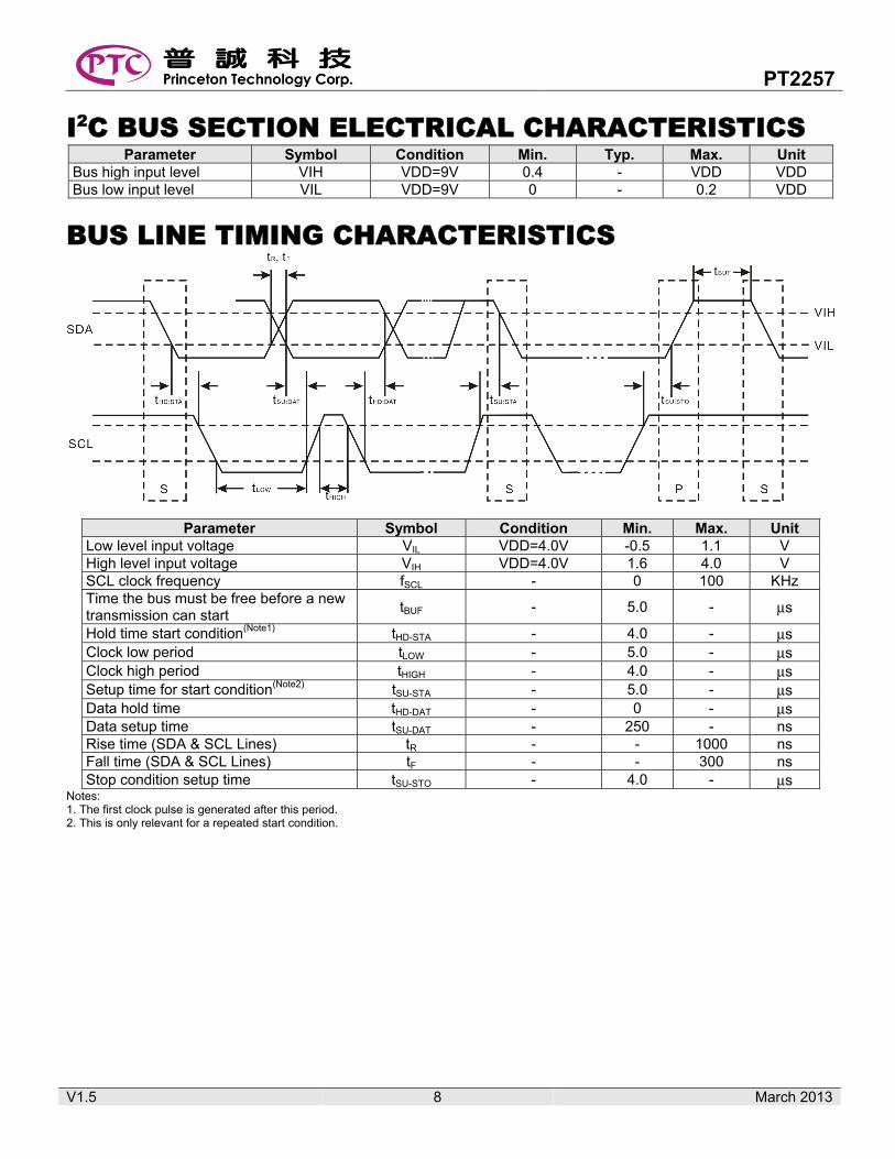
I2C BUS SECTION ELECTRICAL CHARACTERISTICS Parameter Symbol Condition Min. Typ. Max. Unit
Bus high input level VIH VDD=9V 0.4 - VDD VDD Bus low input level VIL VDD=9V 0 - 0.2 VDD
BUS LINE TIMING CHARACTERISTICS
Parameter Symbol Condition Min. Max. Unit Low level input voltage VIL VDD=4.0V -0.5 1.1 V High level input voltage VIH VDD=4.0V 1.6 4.0 V SCL clock frequency fSCL - 0 100 KHz Time the bus must be free before a new transmission can start
tBUF - 5.0 - μs
Hold time start condition(Note1) tHD-STA - 4.0 - μs Clock low period tLOW - 5.0 - μs Clock high period tHIGH - 4.0 - μs Setup time for start condition(Note2) tSU-STA - 5.0 - μs Data hold time tHD-DAT - 0 - μs Data setup time tSU-DAT - 250 - ns Rise time (SDA & SCL Lines) tR - - 1000 ns Fall time (SDA & SCL Lines) tF - - 300 ns Stop condition setup time tSU-STO - 4.0 - μs
Notes: 1. The first clock pulse is generated after this period. 2. This is only relevant for a repeated start condition.
PT2257
V1.5 9 March 2013
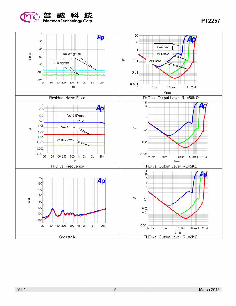
-120
+0
-100
-80
-60
-40
-20
dBV
20 20k50 100 200 500 1k 2k 5k
Hz 0.001
20
0.01
0.1
1
5
%
1m 410m 100m 1 2
Vrms
Residual Noise Floor THD vs. Output Level, RL=50KΩ
0.001
1
0.002
0.005
0.01
0.02
0.05
0.1
0.2
0.5
%
20 20k50 100 200 500 1k 2k 5k
Hz
0.001
20
0.01
0.1
1
10
%
1m 42m 10m 100m 500m 1 2
Vrms
THD vs. Frequency THD vs. Output Level, RL=5KΩ
-140
+0
-120
-100
-80
-60
-40
-20
dB
20 20k50 100 200 500 1k 2k 5k
Hz
0.001
20
0.010.02
0.1
12
510
%
1m 42m 10m 100m 500m 1 2
Vrms
Crosstalk THD vs. Output Level, RL=2KΩ
VCC=3V
VCC=5V
VCC=9V
Vo=2.5Vrms
Vo=1Vrms
Vo=0.2Vrms
No Weighted
A-Weighted
PT2257
V1.5 10 March 2013
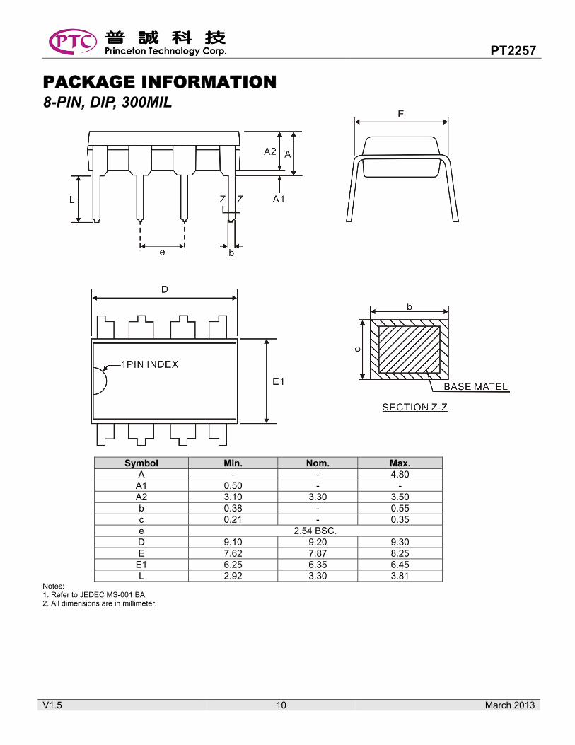
PACKAGE INFORMATION 8-PIN, DIP, 300MIL
Symbol Min. Nom. Max. A - - 4.80
A1 0.50 - - A2 3.10 3.30 3.50 b 0.38 - 0.55 c 0.21 - 0.35 e 2.54 BSC. D 9.10 9.20 9.30 E 7.62 7.87 8.25
E1 6.25 6.35 6.45 L 2.92 3.30 3.81
Notes: 1. Refer to JEDEC MS-001 BA. 2. All dimensions are in millimeter.
PT2257
V1.5 11 March 2013
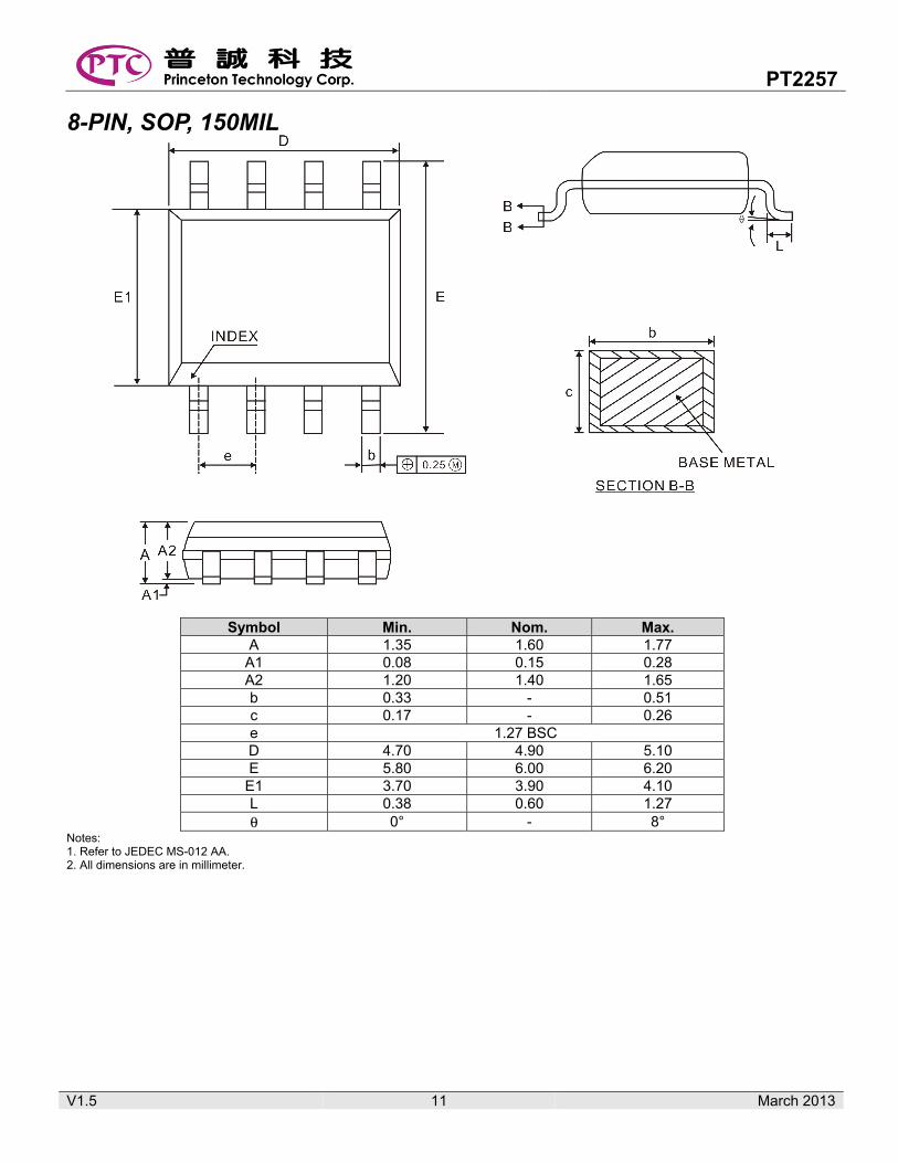
8-PIN, SOP, 150MIL
Symbol Min. Nom. Max. A 1.35 1.60 1.77
A1 0.08 0.15 0.28 A2 1.20 1.40 1.65 b 0.33 - 0.51 c 0.17 - 0.26 e 1.27 BSC D 4.70 4.90 5.10 E 5.80 6.00 6.20
E1 3.70 3.90 4.10 L 0.38 0.60 1.27 θ 0° - 8°
Notes: 1. Refer to JEDEC MS-012 AA. 2. All dimensions are in millimeter.
PT2257
V1.5 12 March 2013
IMPORTANT NOTICE
Princeton Technology Corporation (PTC) reserves the right to make corrections, modifications, enhancements, improvements, and other changes to its products and to discontinue any product without notice at any time. PTC cannot assume responsibility for use of any circuitry other than circuitry entirely embodied in a PTC product. No circuit patent licenses are implied. Princeton Technology Corp. 2F, 233-1, Baociao Road, Sindian Dist., New Taipei City 23145, Taiwan Tel: 886-2-66296288 Fax: 886-2-29174598 http://www.princeton.com.tw


![AC/DC Drivers AC/DC controller IC for LED lighting Included ...rohmfs.rohm.com/jp/products/databook/datasheet/ic/power/...ZT OVP電圧 VZTL 3.250 3.500 3.750 V [ NTC 保護機能 ]](https://img.pdfslide.tips/doc/110x75/60b3a81c87867c7e447abea4/acdc-drivers-acdc-controller-ic-for-led-lighting-included-zt-ovpeoe.jpg)