Embed Size (px)
Citation preview
ELuctmcy aImAcmtrwrIglp 01 G a b SINGLE CItPSUt I10 Dmm SOPWBT OF ns55 PLtm EQPBBILga
(NA,<A-C~-?': eC!*9) E L E C T S I C G L N76- 118d3 C H A " ' ~ . C T E R I Z A ' I I O N O F G a A s S i i 4 G L F C F Y S l A L 2 h I ) L . Y C I SUPIC61 C F R555 FLIGHT E X F E f c : l l E f i T F i n a l T e c h n i c d l ~ l e k c r t ( A ldkdmd univ., Unclas H u n t s v i l l e . ) 6 5 Iic $4.50 C S C L i O r ti3/7b C1897
Final Technical Report
Thls study was supported by the
Space Sciences Laboratory National Aeronautics and Space Admlnietration
Marshall Space Flight Center Harshall Space Flight Center, AL 35812
under Contract NAS8-29542
Depart~ent of Physics School of Graduate Studies and Research The University of Alabm in Runteville
Buntsoille, AL 35807
September 1975
https://ntrs.nasa.gov/search.jsp?R=19760004795 2020-03-22T19:18:16+00:00Z
FINAL TECHNICAL REPORT a3 CONTRACT NAS8-29542
TITLE OF CONTRACT : Elec t r i ca l Characterization of GaAs Single Crystal in
Mrect Support of m55 Flight Experiment
SUBJECT: E lec t r i ca l Characterization of Single Crystal Surfaces
PREPARED BY: J. G. Castle, Principal Invest igator Professor of Physics, UAH
ABSTRACT : The exploration of several nondestructive methods of e l e c t r i c a l characterization of semiconductor s ingle crys ta ls was carr ied out during the period ending May 1974. Two methods of obtaining the microwave skin depth, one for the mapping f l a t surfaces and the o ther fo r analyzing the whole surface OF small s ingle c rys ta l wafers, were developed t o the s tage of working laboratory procedures. The preliminary 35 Qiz data characterizing the two types of space-related s ing le c rys ta l surfaces, f l a t s l i c e s of gallium arsenide and small wafers of germanium selenide, a re discussed. A t h i r d method of nondestructive mapping of donor impurity density i n semiconductor surfaces by scanning with a l i g h t beam was developed f o r GaAs; its tes t ing , done t o a la rge extent without NASA aupport, indicates reasonable pre- cis ion a t reasonable scan r a t e s f o r GaAs surfaces a t room temperature.
SUBMITTED TO : Space Sciences Laboratory, ATTN: ES 12 Lational Aeroanutics and Space Adtlinistration Marshall Space Flight Center Marshall Space Flight Center, AL 35812
SUBMITTED BY : The University of ~ labama i n Huntsville School of Graduate Studies and Research P. 0. Box 1247 Huntsville, AL 35807
September 1975
I..
The author gra teful ly acknwledges the ranp s igni f icant contributions
of h i s supporting s t a f f on t h i s remarkably successful project. Gratitude
goes: t o R. R. Lattanzi, Research Engineer and Paul Zimrerman, Electronic
Technician fo r t h e i r careful learning of some mlcremve techniques,
t o Jaoes H. Roue, Graduate Student, f o r h i s diligence in the success-
f u l op t i ca l scauring of GaAs a t room temperature
t o Michael Valpiani, Senior, f o r h i s e f fec t ive derivation of the
algebra and execution of data reduction fo r the 35 GHz skin e f fec t s f o r
t h i s f i n a l report and
t o Karla Dalton, Sophomore, f o r her mastery of the programing of the
new graphics display terminal s o as t o display the luminescence spectra
automatically ,
but any s h o r t c d n g s i n t h i s report rest with the P. I. The reader is
warned tna t NASA's kindness i n allowing a one-year, no-cost extension fo r
the purpose of improving the write-up does not guarantee the correctness
of the formulae presented herein. The 35 GHz skin depth values were calcu-
la ted from observed power r a t i o s by the use of these formulae for. da ta
reduction and were submitted t o the COR ear ly in the sumner of '74.
TABLE OF CONTENTS
I . INTRODUCTION ............................................... A . Need f o r Nondestructive Method f o r
Elec t r ica l Characterization ............................ B . Noncontacting Techniques fo r High Quality
Single Crystals ........................................ 1 . Use of Radio Frequencies t o Hicrowaves ............ 2 . Use of Optical Radiation ...........................
C . Crystal Selection for this Study ....................... ................................................ D . Purpose
I1 . APPROACH TAKEN ............................................. .................... . A Noncontact ing Techniques Considered
1 . RF Resistance by Coil Loading ...................... 2 . Surface Effects a t 9 6Hz and 35 GHz ................
...................................... . 3 Optical Heans
B . Noncontacting Techniques Used .......................... ............................... . 1 Skin Depth a t 35 Gllz
a . Cavity loading especial ly f o r small s ingle crys ta ls ................................ 1.) The double-arm 35 GHz c i r c u i t used .........
............... 2.) Types of cavity loading used
.......................... b . Waveguide terminat ion
...... 2 . Fluorescence from Electron-Hole Recombination
111 . RESULTS . DEMONSTRATION OF SENSITIVITY OF NONCONTACTMG TEmXQmS ..............................e.............e.s..
................... A . Skin Depths i n GeSe Flake8 a t 35 GHz
B . Skin Depth8 i n G a b Fla t s a t 35 GHz .................... C . Mapping of GaAs Single Crystals by Fluorescence ........
PTR - NAS8-29542
TABLE OF CONTENTS (Contd)
IV. S-Y AND PROGNOSIS ..................................... 29
V. REFERENCES ................................................ 31
APPENDIX A - ASSUMPTIONS FOR EQUATIONS I N APPENDICES B AND C . . 33
APPENDIX B - BASIS FOR LOSS CALCULATIONS FOR CU TEOl REC- TANGULAR CAVITIES FOR f LARGE ENOUGH % SUSTAIN ........................ NORMAL MODE CONFIGURATIONS 38
APPENDIX C - CAVITY LOADING BY SEMICONDUCTOR END W A L L .......... 48
............................ APPENDIX D - GaAe PL DATA REDUCTION 53
PTR - NAS8-29542
I. INTRODUCTION
The NASA program f o r growth of semiconductor s i n g l e c r y s t a l s in the
space environment of Skylab was expected* t o produce c rys t a l s of s i g n i f i -
cant ly higher qua l i ty than a t t a inab le through the same growing processes
on ear th. A s the semiconductor c rys t a l s become more perfect i f undoped
o r more uniform i f doped, t he emphasis in any measurement of them s h i f t s
inczeasingly toward care i n avoiding damage t o t he c r y s t a l by the measurement.
A. Need f o r Nondestructive Method fo r E lec t r i ca l Characterization
E lec t r i ca l character izat ion of a s ing le c rys t a l of semiconductor usual ly
involves "soldering" ohmic contacts in severa l loca t ions i n order t o obtain
some average bulk property (e.g. bulk r e s i s t i v i t y ) f o r the sample piece.
Whenever t he c rys t a l is t o be evaluated f o r use in la rge sca l e integrated
(LSI) c i r cu i t ry , the character izat ion should include a search fo r l o c a l
var ia t ions in e l e c t r i c a l propert ies . Such a search should use a nondestruc-
t i v e method of mapping the surface of the semiconductor.
Clearly, the mapping of e l e c t r i c a l cha rac t e r i s t i c s of high qua l i ty
c rys t a l s , such a s those grown on Skylab f l i g h t s , should be done without
i n f l i c t i n g any damage. To t h i s end, noncontactj.ng methods of mapping were
sought - avoiding the formation of "solder" contacts and avoiding t h e high
l o c a l pressure of point contacts. In addi t ion t o valuable monitoring of
NASA's space processed mater ials , the successful development of s u i t a b l e
noncontacting methods of e l e c t r i c a l measurement would be of considerable
spinoff value t o U. S. semiconductor manufacturers or a t l e a s t t o U. S. semi-
conductor c i r c u i t manufacturers.
*This expectation was real ized many times in ' high qua l i t y semicon- ductor c r y s t a l s grown on the Skylab missions (I . ing 1973 and 1974.
B. Noncontacting Techniques fo r High Quality Single Crys ta l s
The c l a s s of techniques by which the e l e c t r i c a l p roper t ies of
a semiconductor s ing l e c r y s t a l can be observed without contac ts is l imi ted
t o coupling t o t h e c r y s t a l by electromagnetic r ad i a i i on a t frequencies
from r f t o the near uv. The o p t i c a l frequencieshave been used t o probe
the uniformity of ce r t a in types of impur i t i es in semiconductor ~ r ~ s t a 1 s . l
A wide range of rad ia t ion frequencies can be used t o observe the mobi l i t i es
and the concentrations of t he var ious types of charge c a r r i e r s present
near the surface of t h e semiconductor c y r s t a l being examined. For survey-
ing c a r r i e r concentrat ions and mobi l i t i es of t h i n semiconductor shee ts ,
usefu l measureinents of o p t i c a l transmission and r e f l e c t i o n with commercial
instruments have been reported2 with 1.5 mm diameter resolut ion. In
addi t ion, t he impurit ies within t h e semiconductor can of ten be i den t i f i ed
by X-radiation.
Coupling to a semiconductor a t high frequencies implies4 t he react ion
of the semiconductor w i l l take place near t he surface, i .e . , wi thin t he "skin
depth," 6,. The "c lass ica l" appl ica t ion of Maxwell's equations fo r the
case of a f i e l d E, applied t o a plane surface of semi- inf ini te conductor
extending from x = 0 gives t he current densi ty varying with t he depth x
where t h e normal sk in depth, 6,, is defined a s
FTR - NAS8-29542
for p in ohm-meters and f in Hz. The r e s i s t i v i t y , f o r a semicon-
ductor whose dominant charge c a r r i e r has an e f f ec t i ve mass m* and mean-
f r e e time between c o l l i s i o n s of T , can be expreseed6 by the product of T
and t h e c a r r i e r concentration n a s
Usually T and n are each s ign i f i can t i n charac te r iz ing the c rys t a l .
It might be noted in passing tha t t h i s normal sk in depth is small
i n our bes t me ta l l i c conductors even a t power l i n e frequencies. For example,
Equation 2 ind ica tes , as is found i n prac t ice , t h a t 6 2 7 mm in copper and
i n aluminum a t 60 Hz and a t room temperature.
1. Use of h i i o Frequencies t o Microwaves
Returning t o the choice of method t o charac te r ize a f l a t semicon-
ductor c r y s t a l by its r e s i s t i v i t y i n t h e volume encompased by the depth
CC
of x = 6 below the surface, w e can choose t he frequency t o use i n order
t o probe the predetermined depth, 6. Likewise, we can choose t he frequency
t o obtain a -easonable reso lu t ion of t h e mapping s ince t h e minimum sur face
a r ea (= resolut ion element) t ha t can be probed measures approximately one-
half wavelength across. In any case, an instrumental measurement of a
value for the sk in depth a t a given frequency w i l l give, by Equation 2,
t he e f f ec t i ve r e s i s t i v i t y near t he c r y s t a l surface, averaged over t h e a r ea
exposed t o t he rad ia t ion ,
For conducting c rys t a l s , the normal skin e f f e c t app l i e s t o within a
few percent7 with t h e mean-free path of t h e charge c a r r i e r s equal t o one
sk in depth a s given by Equation 2. Values f o r the normal sk in depth a r e ,
by Eq. 2:
For r e s i s t i v i t y of 10 ohm-cm, 6, = 16 amp at 100 MHz,
6, = 1.6 nm a t 10 GHz, and
6 = 0.8 nrm a t 35 GH2. s
For r e s i s t i v i t y of 0.001 ohm-cm, = 0.16 m a t 100 MHz, and
bs = 0.008 mm a t 35 GHz.
Values t o 60 GHz a r e given f o r s i l i c o n i n a recent book by H. F. Matare. 8
Comparison t o c a r r i e r mean-free path, a, can be made by t h e "free electron"
model6 fo r our semiconductor c r y s t a l by est imat ing the Fermi ve loc i ty , vp,
t o be l ( l o 7 ) cm/sec fo r m* = me. The expression f o r mean-free path
is
Values of T = m*wH/e depend on t h e Hal l mobili ty, u ~ . So the values
of mean-free path, 9.. expected f o r "free" e lec t rons i n our semiconductor
a t room temperature a r e estimated t o range from R = 0.4 micron fo r
4 2 yl = 10 cm /Volt s ec t o = 0.04 micron f o r - 1 0 ~ c m ~ / ~ o l t see.
Clearly, we expect a cc 6,.
Therefore, t he c l a s s i c a l expression fo r the sk in depth (6, by Eq. 2)
should be an accurate way of ca lcu la t ing t he r e s i s t i v i t y of f l a t sernicon-
ductor samples from measurement of sk in depth, 6, even a t frequencies
higher than 35 GHz.
Cyclotron resonance and e lec t ron sp in resonance can give useful I
charac te r iza t ion wi th in t h e sk in depth region too. For example, t h e con- 1 i
cent r a t i ons of impuri t ies in G e were recent ly measured9 by cyclotron resonance.
FTR - NAS8-29542
2. Use of Optical Radiation
Coupling t o a semiconductor a t o p t i c a l frequencies can y i e ld elec-
t r i c a l charac te r i s t ica. lo For t h i n semiconductor waf e r e , standard o p t i c a l
( infrared) measurements of r e f l ec t ion and transmission have been used t o
map c a r r i e r concentration and mobility; t he report by Black, e t a1.* indi-
ca tes precision b e t t e r than 10% over a wide range of values f o r GaAs wafers
scanned with a 1.5 mm diameter beam on a Perkin Elmer Model 621 recording
spectrophotometer.
NASA's needs include the a b i l i t y t o character ize t he surface of
more massive semiconductor c rys t a l s - possibly too th i ck t o obta in inf ra red
transmd.ssion values as above. For ce r t a in semiconductors, l ike S i and Ge,
edge contacts w i l l serve t o obtain a map of photovoltaic (PV) response from a
spot of l i gh t impinging on the c r y s t a l surface, reveal ing nonuniformity of
c a r r i e r concentratlon and/or mobil i t ies . Meaningful PV response has
apparently not ye t been a t ta ined on other semiconducror c rys t a l s , such a s
GaAs. For large band gap semiconductors l i k e SIC and G a h , the l i g h t
emitted by electron-hole recombination processes has been used l l s l2 t o i den t i fy
the e l e c t r i c a l l y ac t ive impurity s i t e s present. Our success a t obtaining
impurity concentration i n volumes of GaAs less than a cubic mil l imeter is
mentioned in the Results Section.
Another c l a s s of o p t i c a l techniques which has promise fo r
e l ec t r i ce1 character izat ion involves photo-induced changes. We looked
b r i e f l y for photo-induced conductivity a t room temperature, l3 but our search
was inconclusive. Photo-induced microwave conductivity is s t i l l a poten-
t i a l l y usefu l technique f o r mapping high qua l i ty semiconductor c rys t a l e
without contacts.
C. Crys ta l Select ion f o r t h i s Study
The c r y s t a l s of semiconductors used i n t h i s study of nondastruc-
t ive techniquss fo r observing e l e c t r i c a l c h a r a c t e r i s t i c s were supplied
through the good of f i c e s of t h e NASA Space Sciences Laborator ies, MSFC.
The emphasis during the e a r l i e r port ion was on charac te r iz ing f l a t sur-
feces of G a A s i n preparation f o r t he MS55 Fl igh t Experiment. The emphasis
during t h e l a s t s i x months was on small s i ng l e c r y s t a l l i n e f lakes of vapor-
grown germanium selenide. The comparison of 35 GHz sk in depths w e observed
i n GeSe f lakes grownla on Skylab t o GeSe f lakes grown a t RPI is tabulated
below.
D. Purpose
It was, therefore , t he general purpose of t h i s contract t o demon-
s t r a t e t h e s e n s i t i v i t y of one or more noncontacting methods of e l e c t r i c a l
charac te r iza t ion of s i n g l e c r y s t a l s of t h e semiconductors t o be grown on
Skylab. Spec i f ic goals dea l t a t f i r s t with charac te r iz ing surfcces oC gallium
arsenide s l a b s and dea l t in t h e l a s t ha l f year with small f l akes of germanium
selenide s ing l e c rys ta l s .
Single c r y s t a l samples t o be s tud ied were supplied through the
Space Sciences Lab of NASAIMSFC. The s p e c i f i c approaches t h a t w e inves t i -
gated Included miciowave sk in depth and e-h recombination luminescence. Two L
1
microwave techniques were developed t o t h e point of co l l ec t i ng s t a t i s t i c a l
evidence of sene it i v i t y m d reproducib i l i ty The GaAs lumines cence scanning
technique was developed by an i n t e r e s t ed graduate s tudent J. M. Rare, l a rge ly , !
on h i s o m tine. 1 I
J . -- .< .,, .... -,., . .
FTR - NAS8-29542
11. APPROACH TAKEN
A. Noncontact ing Techniques Considered
RF Resistartce by Coil Loading 1. --
The eddy currents induced i n a semiconductor specimen a r e a spec if!^ I I
i but complicated geometric function of shape of c o i l s and semiconductor and 1
of the uniformity of r e s i s t i v i t y . An example of successful noncontacting 1
measurements of bulk r e s i s t i v i t y by eddy cur ren ts a t 10 MHz was reported
by J. C. Brice and P. Moore i n J. Sci. I n s t . 38 (1961) on page 307. Mapping i i
could be accomplished with s u f f i c i e n t l y small c o i l s but consis tent coupling I is a d i f f i c u l t mechanical problem.
2. Surface Ef fec t s a t 9 GHz and 35 GHz
Preference was given t o 35 GHz because t h e area of t h e mappin8 resolu-
t i on element can be smeller by xl6. We considered the sur face res i s tance
by waveguide termination15 and by cav i ty loading, p r e f e r r ing the l a t t e r f o r
f l a t s wi th high r e s i s t i v i t y and f o r t h e small f lakes . We considered t h e
microwave Hal l e f f ec t . After severa l tries with biomadal c a v i t i e s , we
became more f u l l y appreciat ive of t h e c r i t i c a l need f o r equivalence in t h e
degenerate modes as ca l led f o r by A. M. P o r t i s i n h i s Phys. Rev. pager, a
t r u l y severe mechanical challenge and, therefore , not s u i t a b l e f o r rapid
surveying of f l a t sruaples.
Cyclotron resonance remains a promising prospect9 f o r meamring t h e
l i f e t ime of each type of c a r r i e r provided t h e mapping can be arranged a t
low temperatures.
FTR - NAS8-29542
Phot o-induced changes In microwave conductivity (PC) s imi l a r ly
s tands ar a promising non-contacting way13 of mapping seve ra l e l e c t r i c a l
cha rac t e r i s t i c s with a resolut ion element approaching t h e s i z e of t he
m i n i m u m l i g h t beam. Photo-induced microwave conductivity should be
espec ia l ly useful i n semiconductor samples of very high r e s i s t i v i t y fo r
which the s e n s i t i v i t y of sur face res i s tance measurements is decl ining.
3. Optical Means
Fluorescence from electron-hole recombination is frequent ly a d i r e c t
indicator of the donor impurity d e n s ~ t ~ . l ~ - ~ * The l i t e r a t u r e is l i t e r a l l y
crowded with publ icat ions of such observati.ons f o r semiconductors a t low
temperatures. We found l i t t l e evidence of successful fluorescence a t room
temperature s o we took up t h a t challenge.
Raman s c a t t e r i n g from defect modes a t t he impuri t ies .?f i n t e r e s t
is weak a t room temperature being usual ly not s ens i t i ve enough t o revveal t he
impurity concentrations of i n t e r e s t even a t very low temperatures.
B. Noncontnct ing Techniques I!sed
Each technique fo r noncontacting e l e c t r i c a l cha rac t e r i za t i o r~ of
eemiconductor sur faces was chosen t o demonstrate its r e l i a b i l i t y f o r tibso-
l u t e values in a sample sequence represen ta t ive of t h e sho r t term needs of
NASA's program f o r space c rys t a l l i z a t i on . Repeated subs t i t u t i on of samples
uae employed t o a t t a i n preliminary s t a t i s t i c a l evidence of r e l i a b i l i t y .
It should be noted t h a t t n any sequent ia l subs t i t u t i on method
there a r e sources of dc noise which can be reduced o r eliminated by
properly engineered modulation techniques. Therefore, t he r e l i a b i l i t y or
signa 1-to-noise reported here represent conservative values - euscept i b l e of
improvement by one o r more orders of magnttude with the appropriate engineering.
1-.- -..-....- .- 4 ,-.. . 7 - 4
FTR - NAS8-29542
1. Skin k p t h a t 35 GHz_
Resist ivi ty near a semiconductor surface is related t o the
skin depth, 6,. observed a t the frequency f by Eq. (2) above. The
sens i t iv i ty of the measuring c i r c u i t to small changes in 6, pepends on
the way the semiconductor surface is coupled t o the c i r cu i t . Two s t y l e s
of coupling - cavity loading and waveguide termination - were chosen in
order t o cover a broader range of r e s i s t i v i t y values.
a. Cavity loading, especial ly fo r small s ingle crystals .
The loss introduced in to the c i r cu i t by a sample of semicondu, *tor sur-
face w i l l be a small fract ion of the "no-sample" c i r c u i t losses when
the product1( of the surface area times the skin depth 6, is snall .
This occurs both for small c rys ta ls of normal r e s i s t i v i t y and for
larger sections of large f l a t surfaces of high res i s t iv i ty . Cavity loading
is preferred because i t ra i ses the strength of the electromagnetic f i e l d
a t the semiconductor surface re l a t ive t o its strength i n most other pa r t s
of the detecting c i r cu i t and t h i s leads t o greater sens i t iv i ty t o losses i n
the semiconductor surface than without the cavity.
This sec t ion describes : 1.) the microwave c i r c u i t which
was arranged and cal ibrated t o yield signals r e l i ab ly corresponding t o
absolute cavity parameters and 2.) the type of subs t i tu t ional cavity loading
used. Our analyses fo r converting cavity parameters into value9 of skin
depth of the semiconductor sample a r e given i n the appendices.
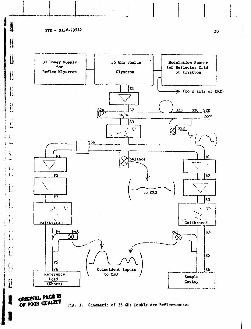
1. ) The double-arm 35 GHz c i r c u i t used. In Fig. 1, the
35 GHz double arm ref lectometer is shown schematically with a r e f l ec t ive
FTR - NAS&-29542
DC Power Supply 35 GHz Source Modulation Source for for Reflector Grid
Reflex Klystron Klystron of Klystron
-. ---.-.-- I-- > ( to x axis of CR
S2C S2D --
I /-
-- ---. ---. ---
. - - 'i- - *' . . --
N- calibrated A
RS
Coincident inputs -,-I... R6 --.
---- --- - -
-& PAGS wm Pig. 1. Schematic of 35 GHz Double-Arm Refleetometer
FTR - NAS8-29542
TABLE 1
COMPONENTS USED I N 35 GHz DEMONSTRATION DOUBLE ARM REFLECTOMETER
Label on Ftgure 1 Item - Function
DC Power Supply
Specif'c Type Mfg. - Model No.
NARDA Model 438
Modulation Source NARDA 438
Kylstron Source of 35 GHz Power Varian VA-9 7
S1 I so l a to r (20 db) TRS A110-95
S2 Direct ional Coupler (20 db) Microline 405A
S2A Matched Load Par t of S2
S2B Frequency Meter (Tunable Cavity) H-P R532A
52C Direct ional Coupler (20db) Elicroline 429A
52D Waveguide Short (Adjustable)
52E Crys ta l Holder (Tunable)
S3 Attenuator (Variable)
S 4 &ic Tee (4 arm)
S5 Crystal Holder (Tunable)
Front Arm
F1
F2
F3
S l ide Screw Tuner ( fo r balancing Tee S4)
I so l a to r (20 db)
I so l a to r (20 db)
Calibrated Attenuator of Rotating Vane
Direct ional Coupler (10 db- broad band)
Demornay Bonardi
Lieco 10V1-26
Demorn~y 3onardi
Demornay Bonardi DBD 919
Uniline by Cascade Res . TRG A110-39
H-P R382A
TRG A561-1C
Table 1 - (Contd)
Label on Figure 1 I t e m - Function --- - F4A Tunable Crys ta l Holder
(Containing MA494 c r y s t a l selected f o r having power response (I vs. Pin) s imi l a r t o t he c r y s t a l i n holder R4A)
Waveguide (connect ion between reference sho r t and f ron t d i r ec t i ona l coupler )
Reference Load - A low lo s s , L g / 4 shor t arranged by F; t o be the same paih length from t h e f ron t F4 d i r ec t i ona l coupler a s t h e sample cavi ty ir is is from the r e a r R4 d i r ec t i ona l coupler.
Spec i f ic Type - Model No. M f g ~ - - - - -
Microwave Associates Mod. 5130
UAH - usual ly included a piece of s t a i n l e s s steel waveguide 20 Xg long 8.448 + .002 inch, h a ~ i n ~ 2 . 2 db round t r i p loss .
UAH - Dug ava i lab le .
Rear Arm - Each correspcnding item is the same model a s i n the f ron t arm, except:
R6 Sample Cavity - usual ly TE015 UAH - assembled copper mode rectangular cav i ty incor- pieces , dugs ava i lab le . porating: 1. Specinl sample holder 2. Fixed (but demountable)
coupling iris.
sample cavi ty on one arm and a high qua l i t y waveguide sho r t on t h e
r e f a l # n c e arm. The list of t h e components used i n t h i s c i r c u i t is given
i n 'liible 1 and points t o t he i den t i ca l cha rac t e r i s t i c s of t he two arms,
i..icluding matching the power response of t h e de tec t ing c r y s t a l s over t h e
Ereqrrency range of some 100 MHz width.
Frequency modulation over one kl:.stron mode piesented
the wo c r y s t a l outputs simultaneously on a double input scope. By
ca re fu l ca l ib ra t ion , including frequent s u b s t i t u t i a ~ l s of standard metal
samples, t h e desired cav i ty r e f l ec t i on coef f ic ien t change was determined
from the change i n t he ca l i b r a t ed a t tenua tor R3 required i n order t o
rematch the CRO t r aces upon each subs t i t u t i on of t he sample. The formulae
used a r e given separa te ly i n an appendix for the d i f f e r e n t types of cav i ty
had ing .
2.) Types of cav i ty loading used. Rectangular TEOlp
mode c a v i t i e s were constructed of milled s ec t ions of copper bc l t ed together
with one s ec t ion carrying a f ixed c i r c u l a r iris1' i n a t h i n (. 020 inch)
w a l l imd one sec t ion mounting the sample. With t h e minimum mil led rad ius of
ins ide corners a t .e l6 inch, we found it necessary t o have the sample
cav i ty a t l e a s t f i v e ha l f wavelengths (p = 5) long. Greater s e n s i t i v i t y
w i l l a c c r u ~ t o sample c a v i t i e s formed t o permit p = 2. The need for t h e
f ixed ris is evident i n the formulae i n the appendices, permit t ing cav i ty
r' dnges upon subs t i t u t i on t o be r e l a t ed so l e ly t o t h e sample. The o r i g i n a l
and still usefu: reference on iris deisgn is MIT Rad Lab Report 43-22 by
H. A. R(?the. 17
FTR - NAS8-29542
Loading of the cavity by a semiconductor surface was done
i n one of two ways: by replacing the end wall o r by adding surface i n
the transverse plane a t one-half wavelength from the end wall. Flat GaAs
surfaces were held a t the end of the rectangular TEOlp mode and leakage
losses were held t o a sa t i s fac to r i ly low level by appropriate choke
joints . Clearly an improved design with much lo re r coupling losses would
involve a sample cavity in the shape of a r ight c i rcular cylinder4 and
the semiconductor f l a t a s i t o end wall o r cent ra l portion thereof.
Thin semiconductor (GeSe) f lakes whose other two dimensions
were under 7 and 3.5 m, respectively, were suspended between two s t r i p s
of p las t i c (sample holder) a t one half wavelength up. Fig. 2 indicates
the microwave magnetic f i e l d pattern in the l a s t two half wavelengths in
the T E o l mode, outlined by the cavity walls and intercepted by the aample
a t one-half wavelength up where the microwave magnetic f i e l d is pa ra l l e l
t o the largest faces of the th in flakes. Our t e s t s indicated no appreciable
mode dis tor t ion by the th in GeSe f lakes used so the obstrved changes in
Q were related t o losses on the GeSe surfaces. We assumed these losses
were conduction losses within the GeSe and calculated the appropriate
skin depths a f t e r integrat ing over the f lake area. 16
b. Waveguide termination. For mapping f l a t semiconductor
surfaces having low r e s i s t i v i t y (below about 1 ohm-cm), the simple termina-
t ion of a waveguide by the sample surface being held across the guide open-
ing w i l l give reasonable sens i t iv i ty . One expects, f o r example, a factor
of 4 in standing wave r a t i o a t 35 GHz for a fac tor of ten i n r e s i s t i v i t y
FTR - NAS8-29542
Fig. 2. One wavelength of the pattern of microwave magnetic f i e ld i n rectangular TEOlp mode sample cavity as viewed through a broad face.
Sample Plane
Credit: George R. Smith for this accurate representation of the H-pattern and its generation using an W 9100 Plotter.
1 - - .... . . - 1
End Wall
FTR - NASd-29542
according t o Lundmayer et a1,15 Aaain, t h e e f f e c t s of leakage on va r i a t i ons
i n the choke coupling can be e f f ec t i ve ly eliminated f o r sur faces f l a t t o
within one o r two degrees over small amp ling a reas by using c i r c u l a r guide.
Our preliminary tests confirmed t h e s u i t a b i l i t y of choke
coupling fo r mapping GaAs f l a t s with a s cu t sur faces when held a s rectangular
waveguide terminations.
2. Fluorescence from Electron-Hole Recombinat ion
The recent surge i n t he semiconductor market for l i g 5 t -
emit t ing diodes fo r o p t i c a l couplers and lasers as w e l l a s f o r d i sp lays has
placed considerable addi t iona l premium on improving semiconductor c r y s t a l
qua l i ty i n t h e category of ga l l ium~luminum phosphide-arsenide. Of spec i a l
i n t e r e s t is thespectrum of luminescence and the dens i ty of donor sites.
Our fluorescence method of surf ace charac te r iza t ion d e a l t d i r e c t l y with
these two propert ies of a GaAs sur face on a reso lu t ion s c a l e of a f r ac t i on of
a mm. Fluorescence measurements a r e inherent ly capable of charac te r iza t ion
on a reso lu t ion s ca l e of t he dimensions of e i t h e r t he c a r r i e r mean-free
path o r the d i f f r a c t i o n limit of t h e o p t i c a l system used t o e x c i t e t h e
c a r r i e r s - whichever is t h e l a rge r fo r t h e sample i n question.
The s t rong market f o r microwave generation and l i g h t
modulation i n Ga-Al-P-As saniconductors merits more d i r e c t measurements of
c a r r i e r l i fe t imes than by standard fluorescence. We suggest op t i ca l l y -
pumped cyclotron resonance should do w e l l .
FTR - NAS8-29542
Our approach was t o use the photoluminescence reported 10.12
f o r gallium arsenide c r y s t a l s a t low temperatures, where the d i f f e r en t kinds
of donor centers can be resolved in the emission spectra , in in t e rp re t ing
the room temperature luminescence. We pumped a spot about 0.5 nnn diameter
on a Gab surface with a l a s e r beam, de l iver ing some 20 mi l l iwat t s a t 632.8 nm,
and col lected the emission over a so l id angle of approximately 0.3 s t e r -
radians not including the angle of specular re f lec t ion . After passing
through a dbuble monochromator a t low resolut ion ( 1 mm s l i t s ) , a narrow band
of t he emitted l i g h t is col lected on a red sens i t i ve photomultiplier tube
(C3893) and t h e output displayed on a chart recorder a s t h e monochr?mator
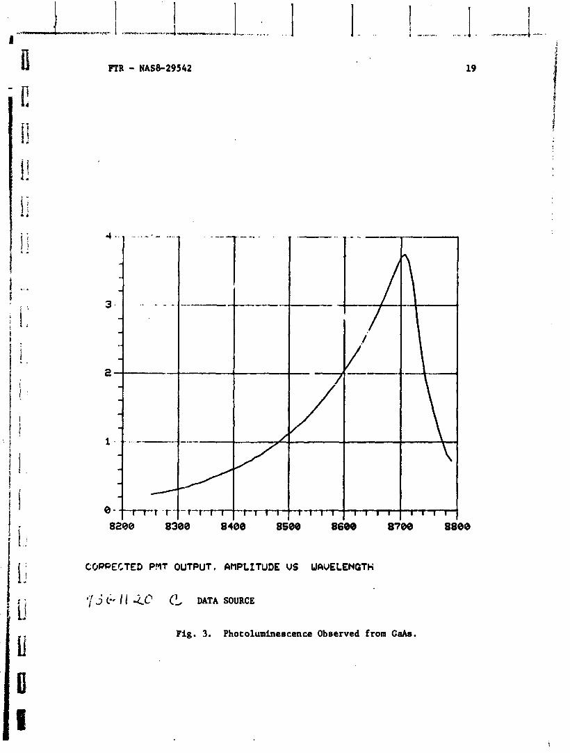
wavelength is scanned from 8200 % t o 8800 1 i n about 10 minutes.
The pr inc ipa l fea tures of a chart record of the room tempera-
t u r e fluorescence from a s ingle spot on GaAs are: t he t o t a l i n t ens i ty , t h e
wavelength of t he maximum in t ens i ty and the widths of the low energy t a i l
and of the high energy s ide . A t yp ica l spectrum from GaAs is displayed in
Fig. 3. Mapping is done e f f ec t ive ly by reposi t ioning the GaAs surface f o r
each spot of i n t e r e s t , with micrometer dr ives .
Credit goes t o Mr. James M. Rowe f o r arranging, ca l ib ra t ing
and tuning up the apparatus t o the s t a t e where w e could scan a s e t of spots
and then get reproducib i l i ty i n t o t a l i n t ens i ty t o within ten percent. The
wavelength fo r t he peak indica tes t he kind of e-h recombination center a c t i v e
(usually a donor s i t e ) . When t h e t a i l s on e i t h e r s i d e a r e narrow, t he t o t a l
i n t ens i ty is r e l a t ed d i r e c t l y t o t h e number of these donor centers being
excited by the pump l i g h t . With the focus and power of t h e pump l i g h t held
constant, the t o t a l emitted in t ens i ty is proport ional t o t he loca!. concentra-
t ion of donors.
Iden t i f i ca t i on of the type of donor s i te by co r r e l a t i on
with the value of the wavelength at t he peak of each spectrum w i l l r equi re
correct ion of t he PMT output t o one proport ional t o t he number of photons
col lected. J. M. Rowe used a standard lamp t o c a l i b r a t e t h e PMT output
and with the a id of Karla Dalton prepared an e f f e c t i v e computer program f o r
carrying out t h i s cor rec t ion procedure. The program's flow char t is given
i n t h e l a s t appendix. The output of t h e program i n i t s present form is
automatic graphing of: t he input spec t r a l da ta , t he corrected PMT output vs. wavelength, and the corrected PKT outprlt vs. energy of t he emitted photons.
Examples of these automatic graphs f o r t h e emission spectrum of one spot
on a GaAs as-cut surface a t room temperature a r e displayed i n Figures 3, 4
and 5.
FTR - NAS8-29542
COPFECTED PMT OUTPUT, 6MPLITUDE US U6VELENGTH
j i- I I L C C, DATA SOURCE
Fig. 3. Phot olumineecence Observed from GaAs .
FTR - NAS8-29542
PMT QUTPUT, AMPLITUDE US WAUELEPCTH
736//.<~; DATA SOURCE
Fig. 4. PL C r ~ m GaAe.
COPPECTEG PVt OUTPUT, AmPLZTUDE US ENERCV(EU2
' I j' &. / I RG ' DATA SOURCE
Fig. 5. PL from GaAe
FTR - NAS8-29542
111. RESULTS - DEMONSTRATION OF SENSITIVITY OF YONCONTACTING TECHNIQUES
In d i r e c t ass i s tance t o the FASA space processing program, t h i s study
has developed three noncontacting technique& in to succe i s fu l laboratory
procedures fo r the nondestructive e l e c t r i c a l charac te r iza t ion of s ing l e
c r y s t a l ~eniconduct ing surfaces . Time permitted only preliminary meamre-
ments with each of the t h r ee procedures, but an ind ica t ion of t h e i r sensi-
t i v i t y is given i n t k - precis ion s t a t e d below f o r t h e measured cha rac t e r i s t i c s .
Valuea obtained f o r t he sk in depth a t 35 GHz and 300 O K i n selected PaAe
sur faces a r e l i s t e d , following a descr ip t ion of t he sk in e f f e c t found i n c.
few of t h e GeSe f lakes grown on S ~ y l a b missions.
A. Skin Depths i n GeSe Flakes a t 35 GHz
The high qua l i ty s ing l e c r y s t a l f l akes protluced by vapor t ransport
in ampules i n Skylab's multipurpose furnace were t h i n p l a t e l e t s a few square
mi l l i ne t e s s i n area. We developed the procedure described above f o r load 1r.g
a room temperature 35 GHz copper cav i ty with one CeSe f l ake a t a time so
t ha t t he cav i ty r e f l ec t i ons could be in te rpre ted t o y i e ld t he r a t i o of t h e
sk in depth averaged over each f l ake t o the skin depth of t he copper wal l s of
the cavi ty . A precis ion measurement of cav i ty Q would then y ie ld a prec ise
value of t h e average 6 in each f lake.
In our preliminary laboratory operat ion, we obtained introductory
information on seve ra l spec i f i c quest ions about t h e use of 35 GHz r ad i a t i on
t o charac te r ize small semiconducting c rys t a l s . F i r s t , our proced;lres a r e
capable of character iz ing without damage the skin depth of each of a la rga
rider ef c r y s t a l s per day. Secondly, center ing of t he sample was judged
v isua l ly and remained one of the p r inc ipa l sources of f l uc tua t ion i n our
FTR - NAS8-29542
observed values. Except f o r more d i f f i c u l t sample handling, the sanre cavi ty
loading procedures work a t l i qu id ni t rogen temperature with the expectation
of even b z t t e r s ens i t i v i ty . Some care must be exercised in the choice of
mater ials fo r holding the sample f lakes in place within the copper cavi ty,
but polyethylene f i lm appears t o serve we l l a t our present s e n s i t i v i t y .
It should a l s o be noted tha t t he sur face cur ren ts induced i n t he f l a t plate-
l e t when properly mounted i n cavi ty are a l l in one d i rec t ion , t he same on
both s ides of the p l a t e l e t , permitting thereby a search f o r anisotropy in
the r e s i s t i v i t y of each semiconductor c rys ta l .
h e operat ional aspect was tes ted - namely the s k i l l l e v e l required
fo r carrying out the cavity loading observations on GeSe a t 35 GHz. After
the selected CeSe f lakes had been measured by a highly experienced operator
(#I ) t o be cer ta in t ha t the loading procedure functioned s a t i s f a c t o r i l y , in
the re r lec t ion cavi ty (A), verbal ins t ruc t ions were given t o a new tech-
nician (operator 2) who had experience with ham radio but none with microwaves.
Operator 2 then surveyed the same samples i n cavi ty A and again in a modified
cavity (B) i n which the end of t he cavi ty had been modified t o permit trans-
miss ion measurements.
The room temperature r e s u l t s a r e summarized i n Tab1.e 2. The r e l a t i v e
Q fac tors (Qs) of each sample t o t h a t (Q,) of the cavi ty wal l s a r e l i s t e d
as an a id t o l a t e r evaluation of t h i s cavi ty loading technique. Pert inent
d e t a i l s a r e l i s t e d i n the appendices.
Inspection of Table 2 shows how the GeSe skin depths vary betweer
these f i v e c rys t a l s by a fac tor of 6. ' h e cor~esponding ra?ge of equivalent
TABLE 2
YaLATIVE Q AND SKIN DBPTHS FOR GeSe RAKES AT 35 CHz AND WOOM TEWERATURE
* Number of ind-yndent substitutions of sauple into cavity.
** Fir& set for operator 2
Calculated with 6,, = 0 . 3 micron
@O Combinations used were Cavity A by operator 1, Cavity A by op?rator 2 , and Cavity B by operator 2.
bulk r e s i s t i v i t i e s is a f ac to r of 36. The unce r t a in t i e s observed would
have been reduced - probably t o - + .003 in %/Qs - by using ten o r s o
independent subst i t u t i-ons of the sample during each run.
The da ta represented i n Table 2 a l s o confirm t h e soundness of our
t heo re t i ca l ana lys i s i n regard t o sample configuration. The absolute
values of t he sk in depth, 6,, l i s t e d in t h e last column of Table 2 con-
firm the v a l i d i t y of t h e f l akes being th i ck compared t o t h e i r own sk in
depth so t h a t t he power l o s s in a f lake is the same kind of product16 of
surface in tegra l s of nT2 a s f o r t he copper wal ls . Secondly, t he f l a k e s were
t h i n enough t o permit using t h e undis tor ted mode values f o r HT across t he
sample.
A f i n a l note about s e n s i t i v i t y of t h i s cav i ty loading subs t i t u t i on
procedure is t h a t when a f l a k e of u l t r a high pur i ty aluminum f o i l was t h e
2 subs t i tu ted load, t he minimum detec tab le a rea was about 3 mm of A l . A s
k . ,
7 ,
the r e s i s t i v i t y of the semiconductor f l ake is increased, our cav i ty loading ; : , . s igna l s become la rger , ind ica t ing t h e capab i l i t y of charac te r iz ing smaller
:
..- f l akes o r of obtaining more precision. For example, t h e observed standard
deviat ions l i s t e d i n Table 2 give: - + 3% f o r a 712 mm2 f l ake having 6, = 1
2 and - + 10% f o r a 1.912 m f l ake having 6, = 6 micron.
B. Skin Depths i n GaAs F l a t s a t 35 GHz
High qua l i t y boules of GaAs glown by M. Rubinstein of Westinghouse
Research snd Development Center i n preparation f o r the M555 Experiment on
Skylab had bee11 s l i c e d fo r character izat ion. Several cu t faces , termed
f l a t s , were mapped f o r sk in depth a t 35 GHz using a reso lu t ion element of
4 x 7 mm as t he rectangular TEOlp cav i ty end wal l i n t he procedure mentioned
above. Cavity r e f l e c t i o n s were interpreted i n accord with t h e ana lys i s out-
l ined i n the appendices i n terms of t h e sk in depth (ts in the GaAs. Some of
t h e average values found f o r bs a r e l i s t e d i n Table 3, taking 6CU 0.35
micron.
TABLE 3
CLASSICAL SKIN DETTH
*A value f o r 6, was not obtainable from t h e data .
Sample
The uncertainty i n the measured v l u e s was much l a r g e r than the l i m i t -
ing uncertainty due s o l e l y t o t he a b i l i t y t o read t h e equipment accurately.
Evidently t he var ia t ions i n r e s i s t i v i t y between t h e a r ea s being sampled a r e
comparable t o but r. )t much l a r g e r than the v a r i a t ~ o n s i n coupling a s an end
wal l i n one posi t ioning of t h e sample. Precis ion improvement of almost one
order of magnitude is expected i n t he same procedure w h e ~ the shape of t he
sample cav i ty is a r i gh t c i r cu l a r cyl inder and the reso lu t ion element of t h e
semiconductor f l a t is t h e c i r cu l a r end wal l o r a concentr ic c i r c u l a r port ion.
1 2 The ac tua l values obtained, however, from the two c a v i t i e s , C s and C s ,
fo r the c l a s s i c a l skin depth of t he samples, a r e i n good agreement. Clear ly
the shor te r cavi ty produces higher precis ion a s expected. Again, when
csl (p=13) 6, (am) cs2 (p-7) 6, (mm)
FTR - NAS8-29542
machining o r e tching techniques a r e used t h a t permit sharper i n s ide
corners (than r = 0.016 inches), then p = 2 c a v i t i e s can be used and
precis ion w i l l be improved over the p = 7 cavi ty .
C. Mapping-of CaAs Single --- Cg-stals by Fluorescence -. -
Photo-induced luminescence of t h e electron-hole recombination radia-
t i on has Laea observed by J. H. Rowe from cut faces ( fLats) of .s.?vercll
high qua l i t y GaAs c r y s t a l s . The technique out l ined above permits mapping
by reposi t ioning the f l a t i n the plane of i t s i r r ad i a t ed face by micrometer
dr ives . A spectrt.m is scanned f o r each posi t ion of t he l a s e r beam spot .
Fig. 3 shows, with t he a i d of automatic graphing on the UNIVAC 1108 computer,
t he t yp i ca l spectrum emitted from a spot on the face of a c r y s t a l doped with
-+1017 donors/cm3. The t o t a l i n t ens i t y (proport ional t c t h e donor concentrb-
10 t i on ) was found t o be reproducible t o + 10% f o r 10 minute s p e c t r a l scans
of the same spot loca t ion and relocat ions. Observed va r i a t i ons across a
sample were occasional ly 50% and were, therefore , a t t r i b u t a b l e t o donor
concentration va r i a t i ons , but no d i r e c t corroboration of t he same surface
p r o f i l e was ava i lab le a t t he t i m e of t h e fluorescence scans. The automatic
correct ion r f Pm output v i a standard lamp ca l ib r a t i on is discussed i n an
appendix and the corrected r e s u l t s p lo t ted i n Fig. 4 and 5 of t h e spectrum
of Fig. 3.
Uniformity of surface roughness probably represen ts t h e u l t imate l i m i t
t c the p r x i s i o n of t h i s high reso lu t ion method of charac te r iz ing t h e donor
concentration. Changes i n t he type of donor w i l l s h i f t t h e peak of t h e
spectrum. For example, ni t rogen donors a r e a few mi l l i e l ec t ron v o l t s below
the band edge a t Eg -1.43 eV. No attempt was made t o c o r r e l a t e peak pos i t ion
FTR - NAS8-29542
with active donor types, but i t is cleat12 that lower temperatures permit
comklete resolution of each type of donor traps.
IV . SUMMARY AND PROGNOSIS
The r e s u l t s of t h i s study of nondestructive methods of e l e c t r i c a l
charac te r iza t ion of t he higher qua l i t y s i n g l e c r y s t a l s of semiconductor
grown i n t he microgravity of space environment include both t h e demon-
s t r a t i o n of successful methods - two microwave and one o p t i c a l - and t h e
measurement of t he r e s i s t i v i t y of a few of t h e small GeSe c r y s t a l s grown
by vapor deposition on Skylab f l i g h t s . The observed s e n s i t i v i t y of t h e
two microwave methods - one f o r mapping l a rge f l a t semiconductor sur faces
and one f o r observing the whole sur face of small t h i n f l a t c r y s t a l s - is
reported f o r a l imited range of r e s i s t i v i t y . The r e l a t i v e skin depth
values f o r the GeSe f l akes s tudied by a sample subs t i t u t i on procedure were
found t o have standard deviat ions around 10% f o r r a the r small c ry s t a l s . The
absolute sk in depth values could r ead i ly have had t h e same precis ion i f
we had made the frequency measurements which lead t o t h e absolute % values.
Our prognosis is opt imis t ic , namely t h a t these room temperature micro-
wave techniques can be car r ied out nondestruct ively using l i g h t weight
apparatus with adequate precis ion f o r weasuring uniformity of r e s i s t i v i t y
of high qua l i t y semiconductor surfaces . Furthermore, r e l a t ed noncontacting
techniques such a s cyclotron resonance and photoinduced wicrowave conduct ivi ty
show promise of being usefu l sources of e l e c t r i c a l c h a r a c t e r i s t i c s of t h e
high qua l i t y semiconductors t o be grown i n space.
The observed reproducib i l i ty of t he fluorescence of room temperature
GaAs under i r r a d i a t i o n a t 632.8 mn of some 10% i n donor dens i ty f o r our
slow scan technique a l so shows promise f o r NASA appl icat ions. Actually,
with the l a rge expansion in t he l i g h t a l u ~ t t i n g diode productian in t h e
FTR - NAS8-29542
past several years, the LED manufacturers very l ikely have a similar
optical scanning technique in regular use by now.
FTR - NAS8-29542
V. REFERENCES
1. c. f . , C. Richard and M. Dugue, "Photoconductivity Associated with Free Excitons in GaAs," Phys. S ta t . Sol. (6) - 50, 263-269 (1972) and references therein.
2. J. F. Black, E. Lanning, and S. Perkowitz, Infrared Physics l0, 125-139 (1970).
3. Consult David P. Nicolas, EC43, MSFCINASA f o r t h e c a p a b i l i t i e s of nondestructiveexaminationby X-ra~ flourescence on h i s scanning e lec t ron microscope.
4. An extended discussion of t h e sk in e f f e c t is given by A. F. Harvey in Microwave Engineering, McGrawfIill Book Co., New York, 1965, p. 256 f f .
5. American I n s t i t u t e of Physics Handbook, D. E. Gray, Ed., McGraw-Hill Book Co., N e w York, 1957, p. 5-85.
6. C. K i t t e l , Introduction t o Solid S t a t e Physics, 4th Ed., J. Wiley and Sons, Inc., New York, 1971, p. 258.
7. AIP Handbook, 1957 Ed., p. 5-200.
8. H. F. Matare, Defect Electronics i n Semiconductors, Wiley I n t e r science, New York, 1971, p. 570.
9. L. E. Blagosklonskaya, E. M. Gersheuzon and Y. P. Lady Zhinskii , "~e termina t ion of the Impurity Concentration i n Germanium by Cyclotron Resonance," i n Soviet Physics - Semiconductors 4 ) 6, 1007 (1970).
10. An exce l len t review of photoluminescence from semiconductors i e pre- sented by H. B. Bebb and E. W, Williams i n Chapter 4 (Theory of Photoluminescence) and Chapter 5 (Photo luminescence i n GaAs) in Vol. 8 of t he book s e r i e s ~emiconductors and Semimetals, R. K. Willardson and A. C. Beer, Ed's., Academic Press, New York, 1972.
11. For SIC, c.f., W. J. Choyke and L. Patr ick, Phys. Rev. B5, 3253 (1972).
12. For GaAs, c.f. E. W. Williams and C. T. E l l i o t t , B r i t . J. App. Phyrr. (J. Phys. D) Ser. 2, Vol. 2, 1657-1665 (1969).
13. Photoconductivity was reported i n r e f . 1 f o r GaAs only at low tempera- tu res .
14. H. Weidemeyer, P, I., Contract NAS8-26146.
15. J. Lindmayer and M. Kutsko, Solid-State Electronics , Pergamon Press, N. Y., 1963, Vol. 6, pp. 377-381.
FTR - NAS8-29542
16. The appropriate integrals are given, for example, by A. F. Harvey in equation 5.2 of ref . 4.
17. c . f . H. A. Bethe, "~umped Constants for Small Irises," MIT Radiation Laboratory Report 43-22, dated March 24, 1943. Unclassif led. 40 pages.
APPENDIX A
ASSUWTIONS FOR EQUATIONS I N APPENDICES B AND C
I f a l l of the microwave energy is stored i n the rectangular
cavity i n only one TE resonant mode, i t is possible t o find a point, O ~ P
E , such tha t the e l e c t r i c f i e l d is 0, independent of the x and y poei- 0
t ions and time. Thue, w e can inse r t a very th in conducting sample a d
a sample holder, made of a d ie l ec t r i c , a t tha t point, with its th in
dimension pa ra l l e l to the z-axis without changing the e l e c t r i c f ie ld .
If ' uH - po, where is the permeability of the s w g i e and
" H is the permeability of the holder, then w e do not change the
magnetic f i e l d and thus the energy stored i n the empty cavity is the
same a s that of the cavity with sample holder with or without the sample.
I f the e l e c t r i c crnd magnetic f i e l d s a r e not a l t e r & within the
cavity by the addition of the sample holder and sample, theu ,ne i n t r i n s i c
Impedance of the cavity has not changed. Thus, the energy r d i a t e d out
the coupling iris, back d m the waveguide should not change. This meane
tha t , fo r case8 (A) through (C) the value of should be the -e.
Similarly, i f , by adding the sample and sample holder t o the empty cavity,
we do not change the current density i n the cavity walle, then the ohlaic
losses due t o the walls is the same i n cases (A) through (C). This can
be done, f o r example, by making the sample holder out of 8 loselees di-
e l e c t r i c so tha t the conducting sample is isolated f r m the walls of the
cavity. A problem can a r i se , however, i n the manner i n which the sample
holder and sample a r e inrerted in to the cavity. I n t h i s par t icular proems,
a s l o t wae cu t in to the r i d e of the cavity. This war that some paver warn
PTR - NAS8-29542
radiated out of the cavity. This l o s s is usual ly neglected in the t o t a l
l o s s of power due t o the wal ls of t he cav i t )~ . We assinnc t h a t adding
the s l o t d id not change the e l e c t r i c and magnetic f i e l d configurat ion
In t h e c a v i t y , and, a s w e a r e i n a T E mode, t h i s m e a m t h a t a t Z o , O ~ P
where t he s l o t was made, the tangent ia l e l e c t r i c and tangent ia l magnetic
f i e l d s a r e both zero. Thus the amount of energy rad ia ted out of t h e
cav i ty is only a small p a r t of the t o t a l wal l losses . Thus, a l t e r i n g
t h i s amount of radiated energy, such a s is cawed by inee r t i ng the
d i e l e c t r i c sample holder i n t o the s l o t , does not s i g n i f i c a n t l y a l t e r t he
t o t a l energy l o s s dueto the wal ls of the cavi ty . Hence the value of
& doesnot change f o r cases (A) through (C). A slmFlar a r g w e n t shows
tha t the value of Q is a l s o a constant f o r cases (D) rhrough (F). W
I f w e assume t h a t the addi t ion of t he second coupling iris does not
change the resonant mode e l e c t r i c and magnetic f i e l d
of t h e s ingle- l ine cavity-coupling system, then QW docs not change from ( ) case (A) through (F) a s the t o t a l energy s tored w i l l be t he same, and the
change i n the energy l o s t due t o the wal l s is not g r e a t l y changed by the
l o s s of t he aurface area, due t o the second coupling iris, from js%2ds,
which is proport ional t o the ohmic energy lo s s per cycle due t o t he wal l s
of t h e cavity,") where HT is the amplitude of the magnetic f i e l d tangent
t o the wal l s of the cav i ty and the i n t e g r a l is taken over t he t o t a l su r f ace
of cavi ty walls. The assumption tha t the addi t ion of the second coupling
i r is does not change the resonant mode is j u s t i f i e d i n the equipment and
c a v i t i e s ueed, by the f a c t t h a t the resonant frequency sh i f t ed by less than
0.1% from the s ingle- l ine cavity-coupling system t o t he two-line cavity-
coupling system.
(1) See E. U. Condon, Rev. Mod. Phyo. 14, P-341 (1942).
Fina l ly , i f the addi t ion of a second coupling iris doe& not change
the e l e c t r i c and magnetic f i e l d s i n the cav i ty , then the value n Qc, 1 is
the same i n cases (A) throu: ' r (C) and caees (D) through (F). Thus, the
values of Qw, Qc, I s 9,. and Qil a r e t he same for cases (A) through (F).
Hence, equation (18) is ju s t i f i ed . It ~ l s o means t ha t t he values of
B1, and B 2 ,
a r e the same i n both t h e s ing le - l ine and two-line cavity-
coupling system, s o t ha t w e can measure bath values by using the s ing le - l ine
cavity-coupling system and use these values i n an equation t h a t is t r u e
fo r a two-line cavity-coupling system. Thus we cen obtain a j u s t i f i a b l e
value fo r Qs using equatiofis (19). (20). and (17) or (17A).
I f w e s t i l l assume t h a t a l l the microwave energy of the rectanaular
cav i ty is s tored i n only one TEOlp mode'and tha t t he e l e c t r i c and magnetic
f i e l d s i n t h i s mode a r e t h e same for t h e coupled cav i ty a s fo r t h e uncoupled
cavity: then the t o t a l energy s tored i n t he empty cav i ty is 1 ly pOH2dv 2
where H is the magnitude of the magnetic f i e l d and the i n t e g r a l i e talcen
over the t o t a l volume of the c a v i t . ~ . I f we i n s e r t our sample and
ohmple holder i n the cavi ty a t the point 2 such t h a t t he e l e c t r i c f i e l d is
zero, then the energy s tored i n the cav i ty with the sample and sample
holder i s the same a s the empty cavity.
A s the sample is conducting, it w i l l c r ea t e an ohmic power l o s s t h a t
w i l l increase the energy lo s s per cycle i n t he cavi ty . The energy l o s s
6 nv per cycle i n the sample is given by . s l8HT2ds where 6, is t h e 2
sk in depth of the sample and H is the magnitude of t he amgnetic f i e l d T
tangent t o t he surface of the sample A and the i n t e g r a l is taken over
the t o t a l surface of the sample. - 2. See Fig . 2 of t h i s report f o r t he shape of the H pa t te rn .
A 8 Qs rn 211(Energy Stored i n t he Cavity) (Energy Lost i n t he sample I n one cycle)
and we have already assumed pa = we ge t ,
Using the so lu t ione fo r the e l e c t r i c and magnetic f i e l d s i n the
TE mode and assuming tha t the *ample i e a rectangular para l le le - O ~ P
piped, we can perform the volume and sur face i n t e g r a l s above, remembering
t h a t t he sample is a t z we ge t , 0'
Where A is the length of the cav i ty along the x-axis, B is the length
along the y-axis, C is the length along the z-axir , Ax i r the length of t h e
sample along the y-axis iy is j t s length along t h e y-axis and y l and
y2 a r e the y posi t ions of the sample i n t h e cavi ty . This r e s u l t a l s o
assumes tha t Az of the sample is s o small that w e cal ignore t h e surface
i n t eg ra l over those port ions of the sur face of the sample t h a t involve Az.
This is j u s t i f i e d i n a l l the GeSe f lakes measured.
Other shapes w i l l ~ r o d u c e other solut ions, however, most shapes can
be approximated by a rectangular paral le lepiped o r a sum of such ehapee,
i n which case, the above equation w i l l s t i l l hold. Otherwi~e , other
4. See Technique of Hicrowave Measurements, Vol 11, edi ted by C. G. Montgmery, P. 295, McGraw-Hill (1947).
coordinate s y s t e m and techniques of in tegra t ion w i l l have t o be used.
Also, note t ha t the Factor of 4 appears i n equation (28), r a t h e r than a
fac tor of 2, t o account for the l o s s 2n t o t h s ides of t he sample, so t?at,
i f a sum of rectangular paral le lepipeds is t o be used as the approxiFa-
t ion, t h i s fac tor can be changed t o 2 and the stm car r ied over both s ides
independently.
Final ly , i f we again have a rectangular paral le lepiped i n which w e
can ignore the Az terms and fur ther , t h a t Ay is s o s m a l l t h a t
s in2 ( i(yl + T)) = sin2(: , then we a r r i v e a t a good approximatior. f o r
Q by assuming tha t Ii2* is a constant over t he t o t a l sur face a rea of t he s
sample; t ha t is
The basic assmpt ion Fn the choke j o i n t cav i ty system is t h a t the
resonant e l e c t r i c and magnetic f i e l d s a r e the same i n a l l four types of
cavi t ies . The same reasoning appl ies i n these s e t s of c a v i t i e s i n
t ransferr ing from the s ing le l i n e cavity-coupling system (cav i t i e s X, Y,
and Z ) t o the two-line cavity-ceupling system (cavi ty T) . Any d i f fe rence
i n microwave energy losses , due t o the choke jo in t , between the 2 cavi ty
and the X cavi ty is taken i n t o account by the Q term. Finally, R, C, H
the same reasoning is used i n ca lcu la t ing the c l a s s i c a l sk in depth, &s'
of the scmple from dw,s,
a s was used i n the proceeding cav i ty system, keeping
i n mind tha t now the sample makes up one c m p l e t e end wal l of the cavity. ?
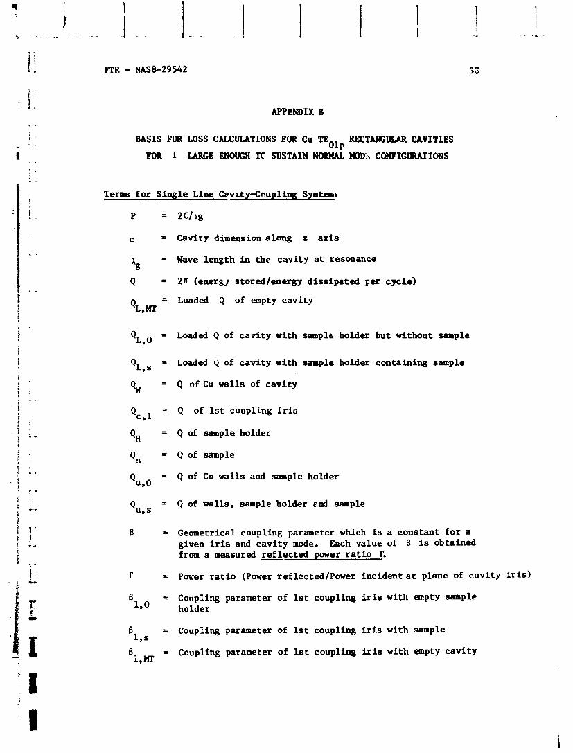
APPENDIX B
BASIS FOR LOSS CALCULATIONS FOR Cu TE RECTANGULAR CAVITIES O ~ F
FOR f LARGE ENOUGH TC SUSTAIN NORMAL, MID?. CONFIG~TIONS
Terms f o r Single Line Cavlty-Coupling Spstesn:
P = 2 c / s
c = Cavity dimension along z a x i s
33 = Wave length i n the cavi ty at resonance
Q = 2n (energ] stored/energy d iss ipa ted per cycle)
= Loaded Q of empty cav i ty Q L , ~
Q ~ , ~
= Loaded Q of cav i ty with sample holder but without sample
QL, s = Loaded Q of cav i ty with sample holder containing sample
QW = Q of Cu w a l l s of cav i ty
Qc , l = Q of 1st coupling iris
QH = Q of sample holder
Qs = Q of sample
QU.0 = Q of Cu wal ls and sample holder
Qu,s = Q of walls, sample holder and sample
B = Geometrical coupling parameter which is a constant f o r a given iris and cav i ty mode. Each value of B is obtained from a measured r e f l ec t ed power r a t i o r.
r = Power r a t i o (Power r e f lccted/Power incident a t plane of cav i ty i r i s )
6 = Coupling parameter of 1st coupling iris with empty sample 1,o holder
B = Coupling parameter of 1st coupling iris with sample 1,s
6 = Coupling parameter of 1st coupling iris with empty cav i ty 1,MT
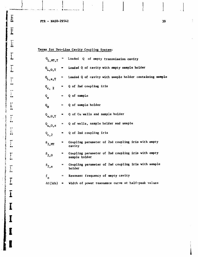
Terms fo r Two-Line Cavity Coupling System:
Q L . ~ , T = Loaded Q of empty transmission cav i ty
QL,O,T = Loaded Q of cav i ty with empty sample holder
QL..,T = Loaded Q of cav i ty with sample holder containing sample
Qc* 2 = Q of 2nd coupling iris
Qs = Q of sample
QH = Q of sample holder
'U,O,T 5 Q of CU wal ls and sample holder
= Q of wal ls , sample holder and sample Qu,o,s
Qc,2 = Q of 2nd coupling iris
'2,m = Coupling parameter of 2nd coupling iris wi th empty
cav i ty
$2,0 = Coupling parameter of 2nd coupling iris with empty
sample holder
B2,s = Coupling parameter of 2nd coupling iris with sample
holder
F = Resonant frequency of empty cav i ty 0
Af(3db) = Width of power resonance curve a t half-peak values
FTR - NAS8-29542
The follawing equations are appl icab le when the lose mechanisms
a r e independent and the microwave energy is s tored i n only one mode.
Basic Equations f o r Single-Line Cavity Coupling System:
A. For the Empty Cavity
B. For Cavity with Bnpty Sample Holder
3. 1 1 - = - + - 1 + - Q1., 0 Qc. 1 Q~ Q~
C. For Cavity with Sample Holder and Sample
7. 1 1 - t - 1 + - 1 + - Qu, s Q~ Q~ Qs
FTR - NAS8-29542
Basic Equations fo r Single-Line Cavity Coupling System (contd)
For t he Empty Cavity
9. 1
I - 1 + - 1 + - Q L , ~ , T Qc, 1 Qw Qc,2
E. For cav i ty with empty sample holder
1 1 = - + - + -- 1 "- QL,O,T
+ - Qc, 1 Qw Qc,2 QH
F. For cav i ty with sample
1 1 14. - = - 1 + - + - 1 + - 1 + -
Q L , ~ , T Qc,1 Qw QH Qs QC, 2
G. Equations fo r ca l cu l a t i ng B
1 . ., 1 *.,, , ." . ,
FTR - NAS8-29542
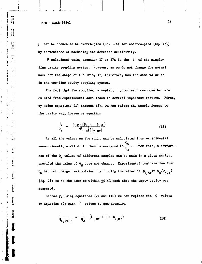
fi can be chosen t o be overcoupled (Eq. 17A) (or undercoupled (Eq. 17))
by convenience of mach in i~a and de tec tor s ens i t i v i t y .
6 calculated using equation 17 or 17A is t h e 6 of t he s ingle-
l i n e cav i ty coupling system. However, a s w e do not change the normal
mode nor t he shape of t he iris, it, therefore , has t he same value as
i n t he two-line cav i ty coupling system.
The f a c t that the coupling parameter, B , f o r each case can be cal-
culated from experimental data leads t o s eve ra l important r e s u l t s . F i r s t ,
by using equations (1) through (8), w e can r e l a t e the sample l o s se s t o
the cav i ty wal l losses by equation
A s a l l the values on the r i g h t can be calculated from experimental
Qw measuresments, a value can thus be assigned t o - . From t h i s , a compari- Qs
son of the Q values of d i f f e r e n t samples can be made i n a given cavi ty , s
provided the value of QW does not change. Experimental confirmation t h a t
had not changed was obtained by f inding the value of B I , ~ ( = Qw/Qc, l )
[Eq. 21) t o be t h e same t o within 9 . 4 % each time the empty cav i ty was
measured.
Secondly, using equations (2) and (10) w e can rep lace t he Q values
i n Equation (9) with 6 values t o ge t equation
As we can ca lcu la te a value f o r ($1 ,nr + 1 + ~ ) , w e c a n t h u s g e t
2 , m a value of Q from a known value of w QL,MT,T . Fina l ly , w e measure t he
value of QL , bfl, T experimentally by using equation
We can a r r i v e a t a value of Q t ha t is W
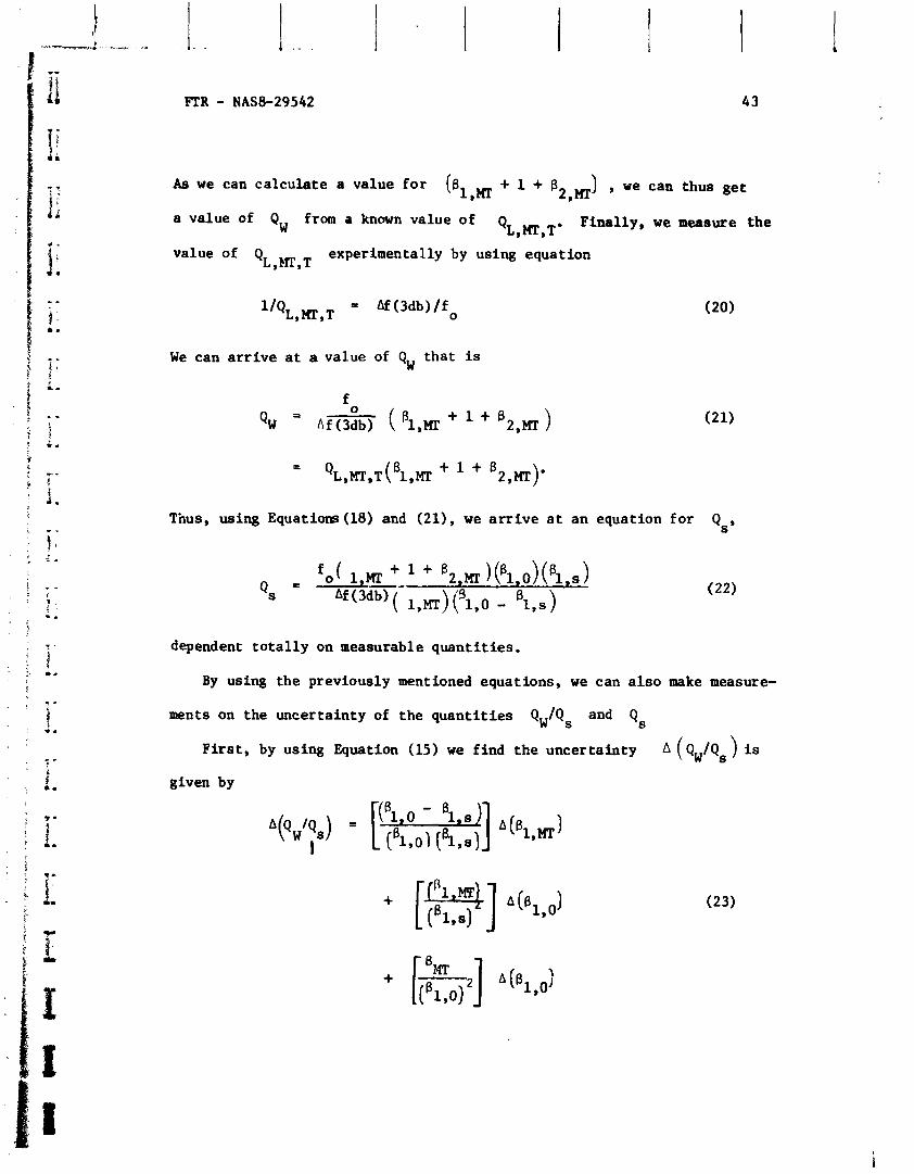
Thus, using Equatiom (18) and (21), we a r r i v e a t an equation f o r Qs,
dependent t o t a l l y on measurable quant i t i es .
By using the previously mentioned equations, w e can a l s o make measure-
ments on the uncertainty of the quan t i t i e s ~ ~ 1 9 , and Qs
F i r s t , by using Equation (15) w e f ind t h e uncer ta in ty A (Q~IQ,) is
given by
FTR - NAS8-29542
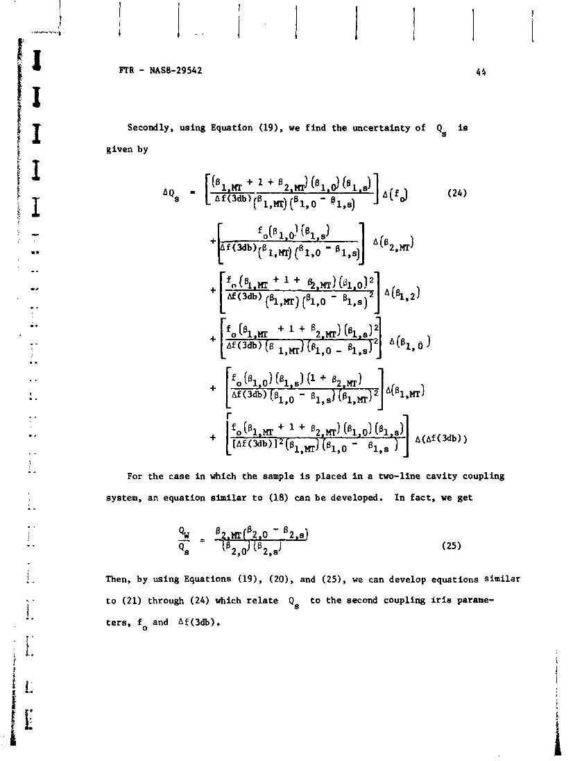
Secondly, using Equation (191, w e f i nd t he uncertainty of Qs is
given by
For t he case i n which the sample is placed i n a two-line cav i ty coupling
system, an equation s imi la r t o (18) can be developed. I n f a c t , we get
Then, by using Equations (191, (20), and ( 2 5 ) , we can develop equations similar
t o (21) through (24) which r e l a t e Qs t o t he second coupling i r i e parame-
t e r s , fo and A f (3db).
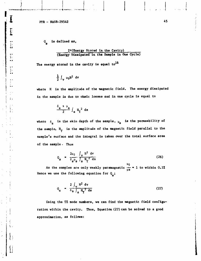
Qs is defined as,
2n(Energy Stored i n . t he Cavity) ( ~ n e r ~ T D i s s i p a t e d i n t h e Sample i n One Cycle)
The energy s tored i n t he cav i ty is equal t o 16
where H is the amplitude of t he magnetic f i e l d . The energy d i s s ipa t ed
i n the sample is due t o ohmic l o s se s and i n one cycle is equal t o
where 6s is the sk in depth of t he sample, us is t h e permeabili ty of
the sample, HT is the amplitude of t h e magnetic f i e l d p a r a l l e l t o the
sample's surface and the i n t e g r a l is taken w e r t he t o t a l sur face a r ea
of t he sample. Thus
lJ 0 A s the samples a r e only weakly paramagnetic - 1 t o within 0.1%
P s Hence w e use t he following equation f o r Q
8 '
Using the TE mode numbers, we can f i nd t h e magnetic f i e l d configu-
r a t i o n within t he cavity. Thus, Equation (27) can be solved t o a good
approximation. a s follows :
( -- . .. . . - . - . - ,, , 3. & .,;uCvn-v -,.
FTR - NAS0-29542
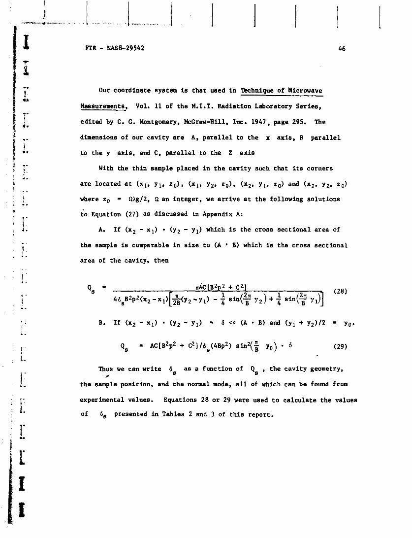
Our coordinate system is t h a t uaed i n 'lkchnique of Hicrawave
Measurements, Vol. 11 of t he M.I.T. Radiation Laboratory Series , - edi ted by C. G. Montgomery, McGraw-Hill, Inc. 1947, page 295. The
dimensions of our cav i ty are A, p a r a l l e l t o the x ax i s , B p a r a l l e l
to the y ax is , and C, p a r a l l e l t o the 2 a x i s
With the t h in sample placed i n t h e cav i ty such tha t its corners
a r e located a t (xl , ~ 1 , z0) , (x l , ~ p , z0) , (x2, ~ 1 , 20) and (xp, ~ 2 , zO)
where z0 = Q&/2, 0 an integer , we a r r i v e a t the following so lu t ions
t o Equation (27) a s discussed Ln Appendix A:
A. I f (x2 - x l ) (y2 - yl) which is the c ross s ec t i ona l area of
t he sample is comparable i n s i z e t o (A B) which is the c ross s ec t i ona l
area of t he cavity, then
B. I f (x2 - x l ) (y2 - yl ) = 6 << (A B) and (yl + y2)/2 = yo.
Qs = A C [ B ~ ~ ~ + ~ ~ ] / 6 ~ ( 4 ~ ~ ~ ) s i n y i yo) 6 (29)
Thus w e can write 6 a s a funct ion of Q t he cav i ty geometry, f
S 8 ' t h e sample posi t ion, and t h e normal mode, a l l of which can be found from
experimental values. Equations 28 o r 29 were uaed t o ca l cu l a t e t he values
of 6s presented i n Tables 2 and 3 of t h i s report .
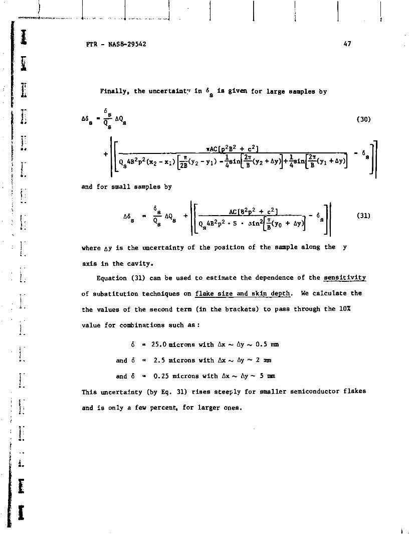
Final ly , the uncertaint:? i n is given f o r l a rge samples by
and f o r small samples by
where ~y is the uncertainty of the pos i t ion of the sample along the y
ax i s i n the cavi ty .
Equation (31) can be used t o es t imate t he dependence of t h e s e n s i t i v i t y
of subs t i t u t i on techniques on f lake s i z e and sk in depth. We ca l cu l a t e t h e
the values of t he second term ( in the brackets) t o pass through the 10%
value fo r combinations such a s :
6 = 25.0micrms with Ax - Ay - 0.5 nun
and 6 = 2.5 microns with Ax - Ay - 2 m
and 6 = 0.25 microns with Ax .- Ay - 5 mm
This uncertainty (by Eq. 31) rises s teep ly f o r smaller semiconductor f l akes
and is only a few percent, f o r l a rger ones.
APPENDIX C
CAVITY LOADING BY SEMICONDUCTOR END WALL
X = The r e f l ec t ive cavi ty with choke and the sample a s an end wa 11
Y = The r e f l e c t i v e cavi ty with choke and a f l a t piece of Cu as an end wall
Z = The r e f l e c t i v e cAvi ty with equal dimensions to X and Y but without a choke
T = The transmission cavi ty
Q c , l = The Q of the f i r s t coupling iris
Qc, 2 = The Q of the second coupling i r is
QR, CH = The Q of the choke jo in t d u e t o microwave energy being
radiated out of the s l o t s of the choke
%,. = The Q of the sample end wall
%. x = The Q of the X cavi ty due t o ohmic losses i n the walls of
the cavi ty except for the sample which a c t s a s an end wall
QW.Y = The Q of the Y cav i ty due t o ohmic losses i n the walls of
the cavi ty except fo r the Cu f l a t , which a c t s a s an end wall
%.z = The Q of the Cu f l a t act ing a s an end wall i n the Y cav i ty
%, end = The Q of the end wall of the Z cav i ty
B = The coupling parameter of the f i r s t coupling i r i s a s 1.u measured i n the cavi ty
= The coupling parameter of the second coupling ir is a s ,e measured i n the cavi ty
FTR - NAS8-29542
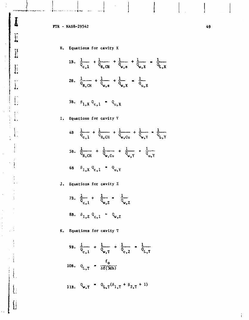
H . Equations for cavity X
3Bw %,x Qc,l P Qu, x
1 I -
Qu, x
I. Equations for cavity Y
3. Equations for cavity Z
K . Equations for cavity T
1 i I. :
-..- --7- - T. - --4 .--Fn..,. *
FTR - NAS8-29542
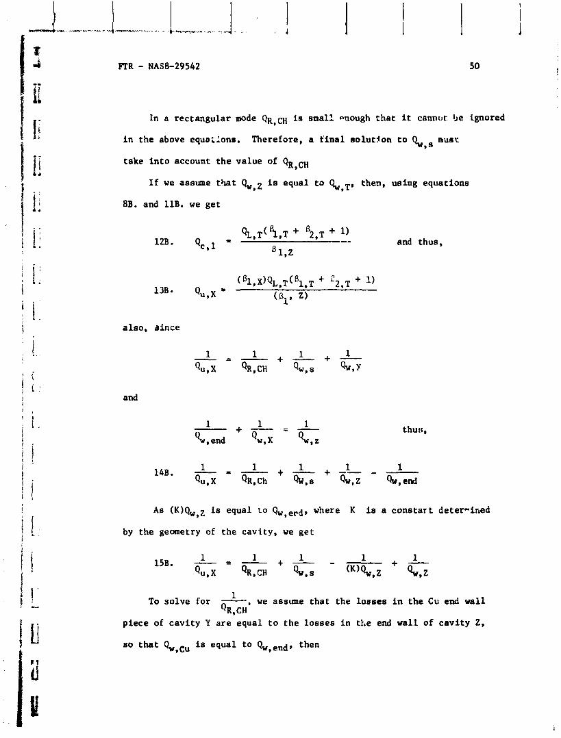
In a rec tangu la r mode QR,cH is smal l nrlough t h a t i t cannut be ignored
i n t h e above equa::ons. Therefore, a f i n a l s o l u t j o n t o must
take i n t o account t h e value of QR,CH
If we assume t b t Qw,Z is equal t o Qw then, us ing equat ions ,T'
88. and 11B. we ge t
a l s o , a i n c e
and thus ,
1 1 1 1 - = - + + - QU,X Q ~ , CH Qw, s Q,
and
1 1 1 + - = - thutl, %I. end Q W , ~ %,z
14B. 1 1 1 1 I -
1 + - + - - - - Qu,x QR, ~h Qw, 8 Qw, z Qw, end
As (K)QWvZ is equal to Qw,ecd, where K i e a constar t determined
by t h e geometry of t h e cav i ty , we g e t
15B. 1 1 1 1 - = - 1 + - - + -
Qu, x QR,CH 9w.s (K)%,z %,z
To so lve f o r - , we assume t h a t t h e l o s s e s i n t h e Cu end w a l l QR,CH
p iece of c a v i t y Y a r e equal t o t h e l o s s e s i n t h e end w a l l of c a v i t y Z,
s o t h a t ssCu is equal t o Qw,end, then
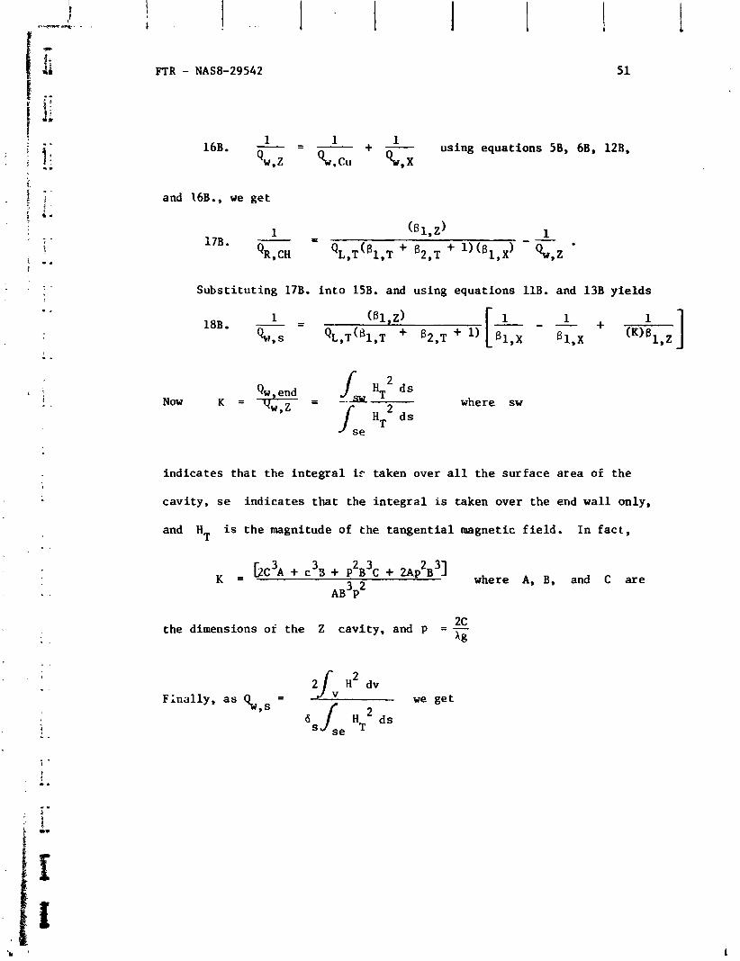
FTR - NAS8-29542
16B. 1 1 - = - 1 + - using equat ions 5B, 6B, 12B,
QW.2 QW.ct1 9Y.x
and IbB., we g e t
S u b s t i t u t i n g 17B. i n t o 1SB. and using equat ions 11B. and 13B y i e l d s
i n d i c a t e s t h a t t h e i n t e g r a l i c taken over a l l t h e s u r f a c e a rea of t h e
cav i ty , se i n d i c a t e s t h a t the i n t e g r a l is taken over t h e end w a l l only,
and H i s t h e magnitude of the t a n g e n t i a l magnetic f i e l d . I n f a c t , T
3 2 3 K = [ ~ c ~ A + c B + P B C + 2Ap2B33] where A, B, and C a r e
A B ~ P ~
2C the dimensions ok t h e Z cav i ty , and P = -
Xg
Finally, a s f /V H* dv
%,s = we g e t
FTR - NAS8-29542
19B. 6s I b2$ + c21 C and
[ s ~ , ~ + c21c 6 - - s 2 2 )2 A(%,s) - - Qw, s * (Qw,s
APPENDIX D
GaAs PL DATA REDUCTION
(by J . M. Rowe)
A computer program has been used t o a i d i n c o r r e c t i n g photolumines-
cence d a t a f o r t h e response of t h e o p t i c a l system, pho tomul t ip l i e r tube
and associa ted e l e c t r o n i c s . Ca l ib ra t ion f a c t o r s obta ined by running a
tungsten ribbon lamp and us ing t h e known emiss iv i ty of tungsten had been
t abu la ted by wavelength every 5 bstween 8010 and 8920 % and were read
i n by t h e computer. The remainder of t h e input cons i s ted of c h a r t r e fe rence
marks and d a t a po in t s i n char t coordinates , a l l taken from t h e record pro-
duced dur ing a d a t a run. Since t h e computer used d a t a i n c h a r t paper
coordinates, much work was saved.
0
During da ta taking, t h e wavelength i n Angstroms was noted at t h e
beginning and end of a run and these po in t s were marked on t h e c h a r t paper.
These wavelengths and t h e i r corresponding coordinates were read i n t o t h e 0
computer and using t h i s t h e computer determined t h e wavelengths i n Angstroms
of d a t a po in t s . This coordinate was taken a s an i n t e g e r f o r convenience.
PL amplitude coordinates were taken as f l o a t i n g point numbers and were
a r b i t r a r y t o wi thin a s c a l e f a c t o r w r i t t e n down dur ing d a t a taking i n c a s e it
would be needed l a t e r .
Each d a t a wavelength was found i n t h e t a b l e us ing l i n e a r i n t e r p o l a t i o n
and the i n t e r p o l a t e d cor rec t ion f a c t o r appl ied. Corrected amplitudes were
each divided by t h e maximum uncorrected amplitude f o r t h e d a t a set t o y i e l d
comparable s c a l e s . This was done f o r convenience. The s c a l e f a c t o r appears
i n t h e p r in tou t and no information was l o s t . The e l e c t r o n v o l t equ iva len t of k
each wavelength was a l s o computed.
FTR - NAS8-29542
The output appears i n tabulated form with f i v e columns. These are:
(1) corrected and scaled amplitude, (2) energy i n e lec t ron v o l t s , (3) wave- a
length i n Angstroms, (4) uncorrected amplitude, and (5) char t coordinate
of wavelength. The l i s t i n g was made i n order of increasing energy, o r
a l t e rna t ive ly fed t o Karla Dalton's program f o r d i sp lay and fo r automatic
graphlng a t t he Tektronix terminal of t he UNIVAC 1108 computer.
The flow chart f o r the PL DATA REDUCTION program is given on the next
page. A l i s t i n g of the program dnd one output t a b l e is at tached, too.
FTR - NAS8-29542
PI, Data Reduction Flow Chart
!Red ca l ibra t ion table (cN!B(I ) ,FAC(I ) ) I I
I
ead char t reference points (FIRST,AFFS T, XLhS T,ALAST) I
d number of d a b s i n t s (NDLITA) 1 \ 1
OF RUN" (STOP
IRead char t coordinates of data points ( ~ ~ P ~ ( I ) , I ~ B ( I ) ) I I
L - - . - . - - -- ---. - - - . -4
(convert coordinates t o hgstrorn u n i t s ( ~ I B ( I ) ) and ( (save maximum - - amplitude ( M ~ x ) 1
I 1 s o r t data by wavelength i n t o increasing order i
I
In terpola te i n t o the table t o f i n d the correc t ion factor . Compute corrected amplitude and divide by AMAX- Call the r e s u l t LU,!P2('L) Compte EHER(I), the electron v o l t equivalent o f -(I). r
Rint "THE SCALE FACTOR ISw A W X
R i n t r e s u l t s ordered by increasing J ~ ~ E R ( I ) .
I Print column h e a d i ~ g s : AMP;!, ENER,XLA:llB,MrP1 , N W . , . - . - -- - - - - --
I
END OF D A U SET" END^
FTR - NAS8-29542
CLAMB ( 1)
FAC( I )
FIRST
AFRST
.!UAST
U S T
NDATA
AMPl(I)
NLAMB (1)
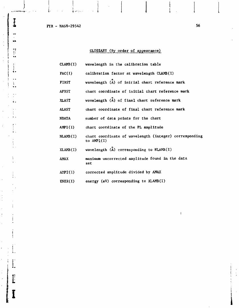
GLOSSARY (By order of appearance)
wavelength i n the ca l ibra t ion t ab l e
ca l ibra t ion fac tor a t wavelength CLAMB(1) 0
wavelength (A) of i n i t i a l chart reference mark
chart coordinate of i n i t i a l chart reference mark
0
wavelength (A) of f i n a l chart reference mark
chart coordinate of f i n a l chart reference mark
number of da ta points f o r the chart
chart coordinate of the PL amplitude
chart coordinate of wavelength ( in teger ) corresponding t o AMPl(1)
wavelength (i) corresponding t o NLAMB(1)
maximum uncorrected amplitude found i n the da t a s e t
corrected amplitude divided by AlWT
energy (eV) corresponding t o XLAMB(1)
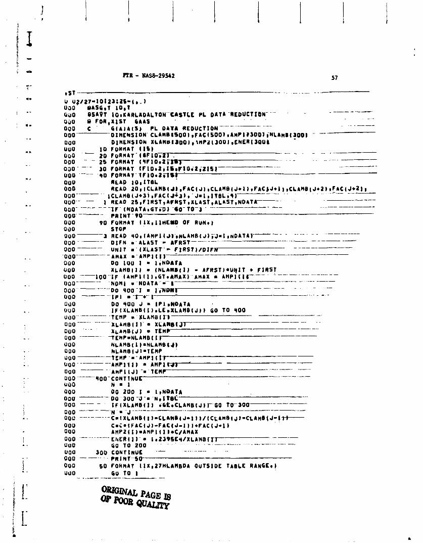
U u 3 / 2 7 - 1 0 t 2 3 $ 2 6 - ( 8 - I 0 3 0 OASG8T 10,T
-. . --.-. - ----. C190 OShVT 108KAULADALtON"'CASTLE -PL OAT& -RLDUCf IPN- "' . - . OdO O FOR,XIST CAAS - -
- .- - ---- 0 0 0 C ‘ - G I A ~ A ~ S J PL DATA R E D U C T ~ O N ~ - - - - - - - - ~ "-- 0 0 0 - D l M E N S l O N ~ C L A M B 1 ~ 0 0 I ~ t A C ~ S O O ~ r A M ? ~ ~ ~ o O ~ ~ ~ L A ~ D ( 3 0 0 ~ - -- 0 0 0 DlMENSION X L A M U ~ ~ ~ ~ I ~ \ M P Z ( ~ ~ ~ ) , E N E ~ I ~ O U ~ 0 0 0 1 0 FORMAT (15) 900 ' - 20 F O R M A T - - I (FIOYZr . 0 0 0 -- --- 2 5 FORMAT ( Y F l O r Z i m
- . - . _ _ _ _ -. _ _--- 0 3 0 - 30 FORMAT ~ F l O v 2 i l S m C l O i 2 i 2 1 5 ~ - -
-- - ....-. ------
0 0 0 ------- 'SO FORMAT- l f 1 0 0 2 f l S t - -.A- -- 0 0 0 RkAD IOmITBL 0 0 0 REAO ~ O ~ I C L A H B ~ J J ~ F A C ( J ) ~ C L A H B ( J + I ~ ~ F A C ~ J + ~ ] ~ C L A H B ( J + ~ ~ ~ ~ A C ( J + ~ I ~ . . . . ... --- 0 0 0 - - - - ~ C L A H ~ ( J * ~ ~ ~ F A C ( J ~ ~ I ~ ~ J ~ ~ ~ I ~ B L ~ Y ~ 000.- '- I REAO 2S8F1RST,AfMSteXLAST8ALAfTiNDATA-- -
.-
0 0 0 - - - - I F - (NDATAr GT.0 8 -60-TO-) - --
---. 0 0 0 ' - - - ?R 1 N T - 9 0 0 3 0 9 0 FOUMAT ( I X o l I H E I D OF RUN.) 0 3 0 STOP 0 0 0 -- 1 READ SO* IAHPI ( J ) *NLAHB( Jli-3.1 i i J D A T A l w e - ' - .
9 0 0 - ----- D fFN m-ALAST.-- A f R S T - - - - I - --
0 0 0 - UNIT r ' l X L A S f ' m F 1 R S T ) / D I F N - .-
' o o o - - - - - - - AMAX = - A M P l t f t - - .-------
000 00 L O O I = I;NDATA 0 0 0 XLAWB(I) r (NLhNS(1 ) - AFRST).UyIT * FIRST 000 '--- 100-IF IAHPI 11 ).GT .&llAX)--AHAX m~ AHPI (It--- -
0 0 0 - - - - - h D H l B -NOATA-6--l-- - - - . - - - - -- - - 0 0 0 - - - - - - ' D O YO0 - 1 . I-#NDI I I
- - - - - - - - . . . - . - -. - -
0 0 0 --.- 1 P I -I--+-t- -----------
0 0 0 0 0 4 0 0 J I P I ~ N D A T A 0 0 0 "00'- *
I F I X L A N B l l J e L E m X L A H B I J ) ) GO 1 0 YO0 t E n P s ~ n r n e c t)
0 0 0 XLAHB( I 1 ' . XL;AllGtJ J --
0 0 0 '
- - - - - -. - - -. x ~ A n e ( J ) - = TEMP
0 0 0 7ERP=NLAMB( 1') -----
0 0 0 N L A H B ( I I = N L A M B ~ J ) 0 0 0 hLAR0( JI.TEMP '
000 ---- TEMP -= 'AMPI I t T -- 0 0 - - - --AHPI I I I = AMP I Mt--L---- ---
0 0 0 --- - A R P I ( J ) - . . T f f l C . - - -. . .
000----'-qOO-CONTlNUE . - - - - - . - -
uiio N . 1 0 0 0 0 0 2 0 0 J * 18NDATA 0 0 9 ---- 0 0 - - 3 0 0 -.a -. . N t a T B ~ -.
0 0 0 - 1F (XLAMB( 1 1 OG&OCLAMB~ JI r G 0 t 0 - - 3 0 U - - - - - 0 0 0
---'- -- N - = --J ----- -- ------- oOg ---.-- C ~ ~ X L A M B I ~ ~ ~ C L A M B ( J - ~ I I / ~ C L L M B ~ J ~ ~ C ~ . A H ~ ~ J ~ ~ ~
0 0 0 C=CelFAC(J)-FACtJ-Ill+FACIJ-II 0 0 0
... . AHP2( I l .AHPI( I l *C/AMAX EIUER ( 1 I . 1 r 2 3 9 S C Y / X L A H B F r 1 - -
0 0 0 .- .. . . .... ..
0 0 0 3 0 0 CON1 INUC - -.... . . .~
0 0 0 ---- - - PR 1 N T--50- - 0 0 0 50 FOHMAT (lX,ZlHLAMBDA OUTSIDE TABLE RANGEr) U0Q Go T O 1 - ----- . --
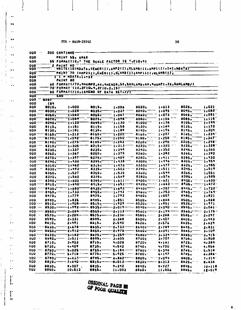
UOO -- 200 CONTINUE 000 PRINT 551 AMAX boo ss F O R M A T ~ I X , * t n ~ SCALE FACTOR IS * , r io .u l OoO - - - . , . - A . - . - - - - - - - - ---- --- ------.- .
000 - - -WRITE I I O I N O A T A ~ ~ E N ~ R ~ ~ I ' ~ A M P ~ ~ ~ ~ ~ ~ L B M B ~ ~ AHPI PI [ I r # I * I - @ N D A ~ A ~ 000- - P R - ~ ~ T - ' ~ o t r n r z t a I , E N L R ~ i ~ ; r i L ~ ~ ~ ~ i ~ i ~ ~ j ~ n ~ r r a J ~ N L A M B I I T i - 000 -1'-m'-NDAf & ,li;h~------------- - -. -- . -- -- 000 r n t n t 80 000 60 ~ O R ~ A T ~ / ~ X ~ ~ ~ A N ? ~ ~ ~ N ~ ~ ~ ~ N ~ R ~ ~ X ~ ~ H X L A ~ ~ ~ ~ X ~ ~ ~ A M ? ~ ~ ~ X ~ ~ H ~ L ~ ~ B / ~ 00U - IO-FORMAT'-t l%c2r'10.q,2F10a2c J S l - - - - .- .-----
000- -
80 ~ O R H A T ~ ~ ~ X ~ ~ ~ H E U O Of DATA SETT/l l 000 LNO 000 --axat 000 1 8q 000 OOlOr l r 000 8OISr 1rOOb 8 0 2 0 ~ 1.013 802Sr 1,021 000 -8030, 1-0028- 1035 r 037---- 80~0,-- 1 a045 801)Srp - l r 0 5 f - 0 0 0 - 8050 a I s 0 6 7 8 0 5 5 7 liO47- 80604--- 1 a073---- 8065r------ 19081- 0 0 0 - 8 0 7 0 1 1 r 0 I l . - 1 0 7 5 r - 1 i 098--- 8080i--- 1 a 106 -- 8 0 8 5 7 - I t 1 1 5 - 000--- 8 0 1 0 7 1 PI 22- 8 0 9 5 7 - l a 1 3 0 ' - ‘ - - ' 8 1 0 0 ( - - - l r 1 3 8 - - OlOSr--. l a l q 9 - 000 8110, l a151 a 1 15a 1 r l S 8 8120b 1.169 a i z s , I r l 7 2 000 8130, l a181 8135e la189 81901 1 a 196 8l '+Sa 1920‘l 000--8 I 5 0 r 1 a 2 1 ~ - 8 i ~ ~ 7 1-a 22O--- 8 160 (--- la227 '- 8165a------ la239- 0 0 0 - 8 1.7 0 7 - 1 a 2 S-P----d 1 7 5 7 T<ZSO- -- 8 180 *-- 1 a 258------ 8185;- 1 267- 000 -1-8 1 9 0 7 I c275- a 1-9 s r 17282- 82oob----- l a290 8 i o 5 r - 1 a 298- OOO-"- - 8 2 1 0 1 - 1 a 305- 8 2 1 S - a 6 l-a-313--- u2zob--- I a 3 Z O - - - 8225;-.-- - la328- 000 8230, 1 a 337 8235, 1 a3rt4 a290, 1 0 352 82Y5r l tJ6O 000 8250, 1 a367 8255r 1 a374 82609 la382 82651 1 a390 O O O - - 8 2 7 0 7 1 a397- 3 2 7 5 7 - l-iq04- - 8280;----- l a 9 1 la--- 8285a------- 1 r 420 0 0 0 ' 8 2 9 0 r 1 ~ a q 3 o - a 2 9 5 a ~ ' a 9 3 8 -' 83006 - - - " ' la996---.- 8305*------ ) r 9 5 9 - 0 0 0 ' 8 3 l O a ~-~P&T-- - - IB~~ST--~ i ~ 7 0 - - 832oF----- 1 a47 7--- 8325*'----- 1,985- 000 - - 8330~--1 a'l93-- - 8335 a- , ---- &,3,,0, l a 5 1 1 83qS1 - - - 1.519. 000 0350a 1 ,527 8355a 1 a535 a3bOt 1 a5YY 8365, 1+551 000 83701 1 a560 8375, 1,569 8J80t 1 r 5 ? 6 8385a 4 r585 000 8390,- laboo- 8s95 ,---- 1 ,h i 1 --- - - aqoob--.--- I .621 ----I r 630- 0 0 0 8 4 l O a - - 8 5 1 ~655--- &,420+---- 1 a663 -- 84%*.-- 11672- 0 0 0 - - - 8 q 3 0 7 . ) i 6 8 7 0 9 3 5 - a - l r 6 9 3 - 8 1 ( 9 0 ) ' ~ ~ * 7 0 7 - - ~ 8995,------ 1.722- 000 - 8950a-- 1 ,733-- I)YS5~---lr742---- 896Utd-- - 1 a753 -*- 8865a----- . 1 ,764- 000 8970a l a779 84751 la793 8q8Ob 19807 8985a la821 000 8990, 1,835 8495 a La851 8500a 1.868 8 5 0 s ~ 1a688 000-- 8510a--- 1 *9O@--- OSISa-- Ia929--BS2Ur------ Ia951--- 8525a- - - - - - - Ia971 000 -- 8530,- 3 ~992-- 8535;-2r014-- 8590t--- Z a O Y O --.- - 8595a 29061- 0 0 0 - - 8 5 5 0 7 2 a 084- 6 5 5 5 r - Z a . t l - ~ - 8 5 6 0 b----- f a 199- 8565;----. 29 175- 000 -- 8570,--- 2 * 204----- 8575--- 21236----. 8580, -- -- - 2a268 - --- 8585,---- 20297 - 000 8590a 2r331 8595 r 21368 8600, zero7 8605 I Za't'43 000 8610. 21991 861Sa 2a590 86201 29576 86251 2,629 000 .- -- --8430*-- 2,678-- 0 6 3 5 ~ 3 a 733--- 869 0 b---- 20789 86$5*--- ' - - - 2a 831 - 000----86SOrp 2r)t-2- 8455 r- ?1?7b-- 9b6Or---- 3a041- 8 6 6 5 ,----- 3a109- UOO ---8670;- 3 c 1 8 2 8 b 7 S i - - 3 ~ tSP---8b8~1-- ja33Y--- 8685;----3eq15- U00 - . 8690.-- - 3r51 a695e--- 3a 605 8790t - - 3a707- - - 8795a 3a808 000 07101 3 r t b 3 07150 4.028 a7201 9.161 8725, 90289 000 8730, '41909 a735a 9,592 87qOa 9 r 700 8795a 9 a 856 U00 -- 8750;-.-5r025--- 8 7 5 5 7 50 189- 87606.- - -- SaJYb . - - 876Sa. - . SaSlU- OUU - 8770r--- 5,718 --- 0775,----- - 5 r 9 2 5 . 87LIOr- 61 1q7 @7@5a 6 a 386- UQO - - - - 8 7 1 0 ; i - 6 0 LS?- 0795a- 6 a 8 6 2 - - ~ - ~ 8 8 0 0 ~ ' - - - - ~ 7 a 0 9 ~ 88051- 7 r319 - 000 -- O l l O r - - - - - - 7,690--- @815-ileOl3- 88204-- 8*313-- 8925*-- Or636 000 8830, 9,007 . 08359 9,392 88YOb 9,727 8895r l O @ l l @ 000 8850, 10e513 0855r 11a003 8860, 11aSOb 8865, I a a 0 1 1
-
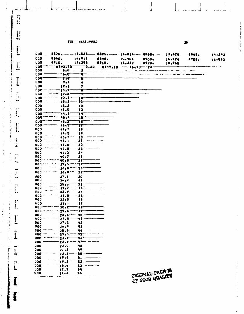
-"..- *.. . I 1 I* ..,'". 1. h. r r.. <+*.:.*a* ,i-.rc=l , .-.. . +. 1 I .I , . I
000 --- [email protected] 1 2 9 b a L - 88IOo -- la*OL1---- 8860,--- . 13r42S. @Yo%, IYr2'42 000 88901 l Y r t l 7 O@tSo 15r *01 0900) 16092y @)O%r 1 b * S L I 000 89100 17m392 'O*lSr C@e232 -6920, 1)rObL uoo- --- 8 7 t t a P b O - - 2 - - 7 5 r l r - -7 3 --- - 000 - - s.0 --. )--- -- ----- -- --- . - ---.-- -------.- - --- . ..- - ~
000 ..
4 *Q '1 - -- -- - -- - .
o o u * w 000 t 6 b 000 1a.l i 00Q 19.7 m 000 - --- A
17.0- I
ooo - - - 22ia-lo 000 - - - -20*s--t! 000 3sr2 i 2 000 41.0 13 000- - 7 i 000 ' I 5 * 1 - 1 $ 0 0 0 - - T S r n 1.' 000 - ------ ' I s . P I - 000 'IY.7 I@ ' 000 TYr2 I t 000 --'-- - 4 3 0 7 " - 2 0 0 0 0 - 3 - 2 1 - 000 ----- 'I2 r-b---2- oo*-.--.- 42*o-- z3---
000 $1.3 29 UOO ooo-. . 9 0 0 7 25
-- $0 0'-- 2 6 - 000 " - 39 *s ---2- 000 . . - 38rO-'-- 211
--- 1800-.'29--
300 37r l 3 0 000 3br2 31 000 '--- - ' -.- . -. --- -a 2----
. 3'4.7 33 OoO -. . .
COO 33 9 oOO- 3 3 r 0 3 7 000 3200 3 6 UUO 3 1 r I 3 7 000 - - - - 30 r 2-30 "oO .- ' . - 29 rs-39 000 2 8 * 6 - - $ 0 UOO 27 08---T1 000 27r2 l a 000 26.S 'I 3 0 0 0 - I - 250 3---- TY 000 - - 2 S r S Y S - - - 000 23. 7- Y4 UOO --. 22rV--Y- 000 22rO Y @ 000 21r2 Y t 000 2ll.a-- . 5 9 000 19.0 51 --------.- uoo )Vr2-----S. 000------ lOrl)-S* 000 17r9 SY 000 17.3 5s
-.
---- --- .- - -. ----
.-A
NOWC -- AccT U A H X X X X X X X X X - PROJECT I QSQSQI------ -.--