Embed Size (px)
Citation preview

FABRICACIÓN Y CARACTERIZACIÓN DECONTACTOS METAL-SEMICONDUCTOR PARA
MICROELECTRÓNCA
Marta Gómez Fernández
Trabajo de Fin de GradoEscuela de Ingeniería de Telecomunicación
Grado en Ingeniería de Tecnologías de Telecomunicación
TutoresStefano Chiussi
María José Moure Rodríguez
2017

Escola de
Enxeñaría de
Telecomunicación
Grao en Enxeñaría de
Tecnoloxías de
Telecomunicación
Mención:
Sistemas Electrónicos
FABRICACIÓN Y CARACTERIZACIÓN DE
CONTACTOS METAL-SEMICONDUCTOR PARA
MICROELECTRÓNICA
Autora: Marta Gómez Fernández
Tutores: Stefano Chiussi, María José Moure
Curso: 2016-2017

1. Introducción
La importancia de los contactos metal-semiconductor reside en que todos los dispositivos electrónicos
basados en semiconductores están unidos a sus terminales externos o a otros dispositivos en el interior de
un circuito integrado a través de contactos de este tipo. Existen dos tipos principales de contacto en
función de las características de la interfase: contacto Schottky y contacto óhmico.
El contacto Schottky presenta un comportamiento rectificante, similar al de la unión p-n, mientras que el
contacto óhmico se caracteriza por presentar un comportamiento lineal (de ahí que se llame “óhmico”,
pues cumple la Ley de Ohm) y una resistencia prácticamente despreciable en comparación con el resto del
dispositivo, de forma que la existencia de este contacto no interfiera en las características eléctricas del
dispositivo.
Los contactos Schottky (también llamados de barrera o rectificantes) tienen importantes aplicaciones como
los diodos Schottky o los transistores MESFET. La principal característica de los contactos rectificantes es
que permiten trabajar a altas velocidades, y por ello, son muy utilizados en aplicaciones de alta frecuencia
como conmutadores. También se utilizan como diodos rectificadores de potencia ya que disipan fácilmente
el calor a través del contacto metálico.
Los contactos óhmicos se utilizan para unir los terminales metálicos de salida de un dispositivo electrónico
al semiconductor, de forma que la resistencia del contacto sea muy baja y no se vean afectadas las
características eléctricas por la existencia del contacto metálico. Por esta razón los contactos óhmicos
suelen ser omitidos en los esquemas o diagramas, ya que están pensados para no influir en el
comportamiento dispositivo.
Figura 1. Estructura de un dispositivo electrónico con contactos óhmicos
Teóricamente, para lograr un contacto óhmico entre un metal y un semiconductor tipo n, la condición que
se debe cumplir es que la función de trabajo del metal sea menor que la del semiconductor (o mayor, en el
caso de que sea un semiconductor tipo p). Por desgracia, existen muy pocas combinaciones que cumplan
este requisito y por ello, la alternativa más común es crecer una capa fuertemente dopada sobre el
semiconductor, para que el espesor de la región de carga espacial sea muy pequeño así como el espesor de
la barrera de potencial, de forma que se permite fácilmente el paso de los electrones a través de la barrera
por efecto túnel, es decir, la barrera de potencial en la interfase metal-semiconductor es tan pequeña que
los electrones puedan atravesarla en lugar de sobrepasarla. Generalmente, la capa fuertemente dopada se
consigue por reacción a alta temperatura del semiconductor con una aleación del metal de contacto y otro
elemento que actúe de impureza donadora o aceptadora [1].
El estudio de los contactos metal-semiconductor se basa en el modelo de afinidad electrónica (EAM), que a
pesar de ser un modelo puramente teórico explica adecuadamente ciertos aspectos y es por ello por lo que
se sigue utilizando. Sin embargo, en la práctica los contactos reales no se ajustan a este modelo y la
corriente es controlada por el ancho de la barrera de potencial en lugar de la altura, como se explica en el
modelo EAM [2].
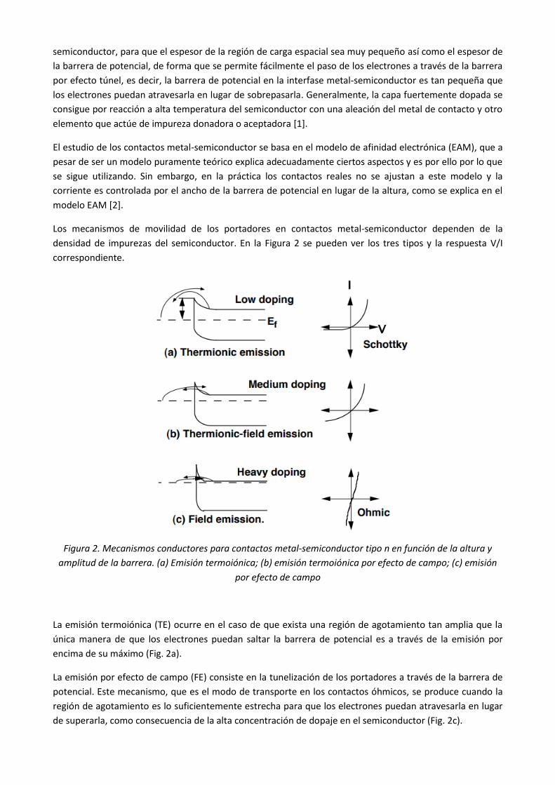
Los mecanismos de movilidad de los portadores en contactos metal-semiconductor dependen de la
densidad de impurezas del semiconductor. En la Figura 2 se pueden ver los tres tipos y la respuesta V/I
correspondiente.
Figura 2. Mecanismos conductores para contactos metal-semiconductor tipo n en función de la altura y
amplitud de la barrera. (a) Emisión termoiónica; (b) emisión termoiónica por efecto de campo; (c) emisión
por efecto de campo
La emisión termoiónica (TE) ocurre en el caso de que exista una región de agotamiento tan amplia que la
única manera de que los electrones puedan saltar la barrera de potencial es a través de la emisión por
encima de su máximo (Fig. 2a).
La emisión por efecto de campo (FE) consiste en la tunelización de los portadores a través de la barrera de
potencial. Este mecanismo, que es el modo de transporte en los contactos óhmicos, se produce cuando la
región de agotamiento es lo suficientemente estrecha para que los electrones puedan atravesarla en lugar
de superarla, como consecuencia de la alta concentración de dopaje en el semiconductor (Fig. 2c).
El ancho de la región de deplexión, Xd, en la interfase metal-semiconductor se calcula a partir de la
siguiente fórmula:
Para conseguir el efecto túnel, Xd debe ser del orden de 3 nm o inferior, con lo cual, la concentración de
dopantes mínima necesaria se calcula despejando Nd en la anterior expresión.
Se trata de un valor relativamente fácil de conseguir en la fabricación de dispositivos, por lo que es la forma
habitual en que se realizan los contactos en circuitos integrados [2, 6, 15, 16].
Una explicación más detallada sobre contactos metal-semiconductor a nivel teórico se encuentra en el
Anexo 1.
2. Objetivos
El objetivo de este Trabajo de Fin de Grado es fabricar y caracterizar por primera vez contactos óhmicos
metal-semiconductor en el laboratorio del Grupo de Nuevos Materiales (FA3) del Departamento de Física
Aplicada de la Escuela de Ingeniería Industrial.
Este objetivo se divide en pequeñas fases que se han ido cumpliendo durante el desarrollo del trabajo:
1. Determinar los requisitos de la oblea (conductividad, concentración de dopantes).
2. Determinar el espesor mínimo de aluminio que garantice la resistencia de contacto mínima.
3. Desarrollar un sistema de medida que permite obtener la curva V/I.
4. Calcular la resistencia de contacto usando una versión adaptada del método TLM.
5. Validar el proceso de fabricación (limpieza, evaporación, recocido).
La motivación de este TFG surge tras las investigaciones del Grupo de Nuevos Materiales sobre elementos
del grupo IV. Los objetivos de estas investigaciones en un futuro a largo plazo son mejorar la velocidad de
computación y minimizar el calentamiento de dispositivos CMOS, entre otros, mediante nuevas aleaciones
del grupo IV, como el GeSn, que ya se ha producido en el laboratorio mediante procesos asistidos por
técnicas láser.
Pero antes de poner la vista tan lejos, es necesario probar por primera vez que las técnicas de crecimiento y
estructuración por láser funcionan para fabricar dispositivos con materiales conocidos como el Silicio o
Germanio. Se inicia así una serie de pasos que basándose cada uno en los resultados de los anteriores se
encaminan a conseguir fabricar dispositivos con los materiales recientemente descubiertos y cuyo primer
paso es la fabricación de contactos metal-semiconductor.
En el Anexo 2 se profundiza un poco sobre el estado del arte de este TFG.

Por último, en términos más generales, otros objetivos subyacentes del trabajo son la familiarización con la
sala blanca y sus protocolos de trabajo, el manejo de diversas técnicas e instrumentos de laboratorio
utilizados en procesos de fabricación microelectrónica y comprender la importancia de trabajar en un
entorno ambientalmente controlado y libre de impurezas, cumpliendo diferentes partes de la norma ISO
14644.
3. Metodología
3.1. Sala blanca
La fabricación de dispositivos semiconductores microelectrónicos requiere disponer de unas instalaciones
ambientalmente controladas y libres de contaminantes. Los procesos de fabricación de dichos dispositivos
se ven afectados por la contaminación debida a polvo o microorganismos presentes en la atmósfera. Estos
contaminantes pueden impedir que el dispositivo funcione correctamente, modificar sus propiedades o
reducir su fiabilidad, ya que una partícula, de tamaño en torno a un 10% del tamaño total del circuito,
depositada sobre él, provocaría la destrucción o inutilización del circuito en la mayoría de los casos. Por
ello, se hace necesario disponer de una sala blanca (o sala limpia) en la producción de tecnología
microelectrónica, como la del Departamento de Física Aplicada.
Además, durante el desarrollo de este proyecto se han revisado y mejorado algunos Procedimientos
Normalizados de Trabajo (PNT) del laboratorio, todos ellos redactados en inglés para facilitar la
incorporación de alumnos Erasmus e investigadores. Todos los PNTs que se usaron y revisaron se citan más
adelante.
En el Anexo 3 se amplía la información sobre qué es una sala blanca, sus características, clasificación,
protocolos, control de partículas, etc.
3.2. Corte y limpieza de las muestras
Se utilizaron diferentes obleas de silicio monocristalino, cuyas características se detallan en la tabla III. El
proceso de preparación de las muestras comienza por cortar las obleas en cuadrados de aproximadamente
1x1 pulgadas, numerarlas y por último limpiarlas (Anexo 11, Figura 1). En el anexo 4 se detalla este
procedimiento.
La limpieza de las muestras se hace en dos fases: la primera tiene como objetivo eliminar cualquier tipo de
residuo orgánico y la segunda, eliminar la capa de óxido nativo (SiO2) presente en la superficie del silicio.
Para eliminar la contaminación orgánica se introducen las muestras en una solución piranha, formada por
ácido sulfúrico y peróxido de hidrógeno (H2SO4: 30% H2O2; en proporción 3:1) durante 10 minutos; a
continuación, se enjuagan con agua desionizada (R > 10 M·) y se hacen dos baños de ultrasonidos de 5
minutos cada uno; por último, se secan con la pistola de nitrógeno (99.96%).
La segunda fase de la limpieza consiste en introducir las muestras en una disolución de ácido fluorhídrico al
8% (40%HF: H2O; 1:5) durante unos 20 segundos o hasta que comprobemos que el óxido ha sido eliminado
observando el cambio de hidrofobicidad de la superficie. Después se enjuagan nuevamente con agua
desionizada un par de veces y por último se secan con N2.

Esta fase de limpieza previa al depósito del metal es de vital importancia para lograr un buen contacto
óhmico entre el metal y el semiconductor ya que depende en gran medida de las características de la
interfase entre ambos materiales. [5].
En el anexo 5 se completa la información del proceso de limpieza de Si, así como en los anexos 6 y 7 se
explica cómo realizar las citadas disoluciones.
3.3. Depósito de aluminio
En el proceso de fabricación de componentes microelectrónicos una de las fases más importantes es la
metalización, esto es, la deposición de una capa de metal sobre el sustrato para la creación de contactos o
pistas de interconexión entre los diferentes elementos. La mayor parte de los fallos que se producen en los
circuitos integrados son debidos a defectos en el proceso de metalización, por ello, la elección del metal
adecuado es la base del éxito de este proceso.
Para este trabajo se ha utilizado el aluminio, ya que es uno de los metales más usados para crear contactos
óhmicos principalmente debido a su baja barrera de potencial, alta conductividad y bajo precio.
La técnica de metalización más utilizada en general, y elegida en este proyecto, es la deposición física en
fase vapor (PVD, según sus siglas en inglés, Physical Vapor Deposition). Es una de las técnicas más sencillas
para crear capas delgadas (hasta 2 µm) sobre un sustrato. El principio físico utilizado en la deposición es la
evaporación térmica al vacío, que consiste en calentar el aluminio en una cámara de vacío hasta su
evaporación, de forma que los átomos de aluminio en estado gaseoso se adhieran por condensación sobre
el sustrato colocado encima.
Antes de hacer el depósito se colocan sobre las muestras las máscaras de electrodos. Se dispone de tres
máscaras con diferentes distancias entre electrodos, las cuales se analizarán posteriormente. Una vez
colocadas las muestras, se procede a preparar la cámara de vacío donde tiene lugar el depósito. Siguiendo
las indicaciones del PNT, al cabo de unos 30 minutos la presión de la cámara baja hasta los 10-7 mbar, y por
tanto, ya se puede realizar el depósito (Anexo 11, Figura 2).
En el Anexo 8 se explica con detalle el proceso de evaporación térmica.
3.4. Caracterización de contactos
Después de haber creado los contactos, es necesario conocer la separación entre ellos, su tamaño y el
espesor de la capa de aluminio, aunque de esto último ya tenemos una aproximación proporcionada por el
sensor de cuarzo instalado en el interior de la cámara de vacío, que proporciona una medida de espesor “in
situ” del proceso de evaporación. Para llevar a cabo medidas de espesor “ex situ” se emplea la técnica de
perfilometría mecánica (Anexo 11, Figura 3).
La perfilometría mecánica o de contacto es una técnica de análisis superficial 2D, basada en una punta de
diamante o estilete (en inglés: stylus) usada para caracterizar topográficamente superficies. La técnica
consiste en la medida del desplazamiento vertical que se produce en el estilete mientras se realiza un
barrido lineal manteniendo constante la fuerza que éste realiza sobre la superficie de la muestra (la
longitud de barrido y la magnitud de la fuerza pueden variarse en función de las características de la

muestra). La punta está conectada a un sistema de medición que graba los desplazamientos verticales que
sufre en su recorrido a lo largo de la superficie de la muestra.
En la realización de este Trabajo se utilizó el perfilómetro de contacto disponible en el laboratorio del
Grupo de Nuevos Materiales, el Dektak3 ST (Veeco). Este equipo dispone de una punta de diamante de
radio 2,5 µm, rango vertical desde 10 nm hasta 131 µm y resolución vertical de hasta 1 nm. La máxima
longitud que permite analizar es 50 mm con un máximo de 8000 puntos.
Se analizaron las muestras FP1-FP12 para determinar la separación entre los contactos, cuyos resultados se
muestran en la tabla I.
Tabla I. Resultado de las medidas de la distancia entre electrodos.
Máscara Valor medio (µm)
“pequeña” 480 ± 16
“media” 700 ± 29
“grande” 1520 ± 39
En la tabla II se detallan los resultados de las medidas del tamaño de los contactos, para las cuales se
analizaron las muestras FP58, FP59, FP78 y FP81.
Tabla II. Resultado de las medidas del tamaño de los electrodos.
Máscara Área contacto
“pequeña” 9 mm2
“media” 9 mm2
“grande” 8 mm2
En el Anexo 9 se explica el uso del perfilómetro Dektak3ST.
3.5. Recocido térmico
El recocido (o thermal annealing, en inglés) es un tratamiento térmico que consiste en calentar los
materiales hasta alcanzar una temperatura determinada y luego enfriarlos lentamente en el interior del
horno hasta alcanzar la temperatura ambiente.
En la realización de este TFG, esta técnica se usa para mejorar el contacto entre el aluminio y el silicio,
puesto que al calentarse el metal sobre el silicio, la interfase entre ambos materiales mejora ya que la capa
de óxido de silicio que puede existir incluso después de la limpieza con HF, al ser sometida a altas
temperaturas se diluye en el aluminio y además se difunde el aluminio en defectos del cristal de silicio
(spiking) y de esta forma se obtiene una mayor adherencia del contacto [3, 12].
La finalidad de este paso es reducir la resistencia de contacto entre metal y semiconductor.

4. Resultados
Para saber si los contactos creados son óhmicos o no y determinar su resistencia de contacto, se obtiene la
curva característica V/I donde se puede comprobar fácilmente si el comportamiento es o no lineal. Para
medir las muestras se ha fabricado una caja aislante con unas puntas de alta conductividad que van
conectadas al analizador de potencia Agilent N6705A DC Power Analyzer del laboratorio de
microelectrónica de la Escuela de Ingeniería Industrial.
4.1. Influencia de la concentración de impurezas de dopaje
Para valorar la influencia de la concentración de impurezas en la obtención de un contacto óhmico es
necesario agrupar las diferentes muestras en función de este parámetro. Se detallan sus características más
relevantes en la tabla III.
Tabla III. Características de las obleas de Si
Nº muestras Tipo dopante Concentración impurezas (a/cm3)
Resistividad (Ω·cm)
1-12 tipo n (P) > 8,9×10¹³ 1-50
57-89 tipo n+ (As) > 2,1×10¹⁹ < 0,005
En la Figura 3 se representa la curva V/I de las 12 muestras correspondientes a la oblea tipo n, con 1013
átomos de fósforo/cm3.
Figura 3. Curvas V/I de diferentes muestras con Si dopado tipo n
A continuación, en la Figura 4 se comparan 4 de las muestras representadas en la imagen anterior junto con
una muestra de la oblea altamente dopada. Se eligieron las muestras FP3, FP6, FP9, FP12 y FP70.
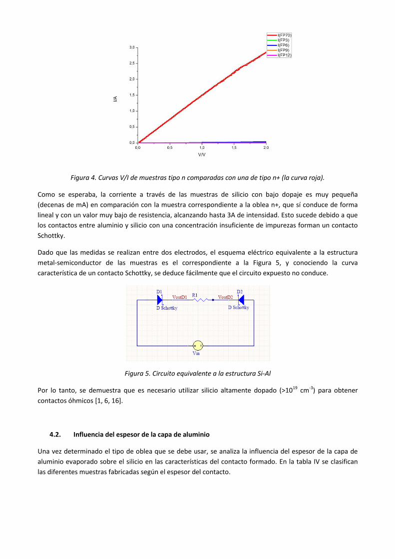
Figura 4. Curvas V/I de muestras tipo n comparadas con una de tipo n+ (la curva roja).
Como se esperaba, la corriente a través de las muestras de silicio con bajo dopaje es muy pequeña
(decenas de mA) en comparación con la muestra correspondiente a la oblea n+, que sí conduce de forma
lineal y con un valor muy bajo de resistencia, alcanzando hasta 3A de intensidad. Esto sucede debido a que
los contactos entre aluminio y silicio con una concentración insuficiente de impurezas forman un contacto
Schottky.
Dado que las medidas se realizan entre dos electrodos, el esquema eléctrico equivalente a la estructura
metal-semiconductor de las muestras es el correspondiente a la Figura 5, y conociendo la curva
característica de un contacto Schottky, se deduce fácilmente que el circuito expuesto no conduce.
Figura 5. Circuito equivalente a la estructura Si-Al
Por lo tanto, se demuestra que es necesario utilizar silicio altamente dopado (>1019 cm-3) para obtener
contactos óhmicos [1, 6, 16].
4.2. Influencia del espesor de la capa de aluminio
Una vez determinado el tipo de oblea que se debe usar, se analiza la influencia del espesor de la capa de
aluminio evaporado sobre el silicio en las características del contacto formado. En la tabla IV se clasifican
las diferentes muestras fabricadas según el espesor del contacto.
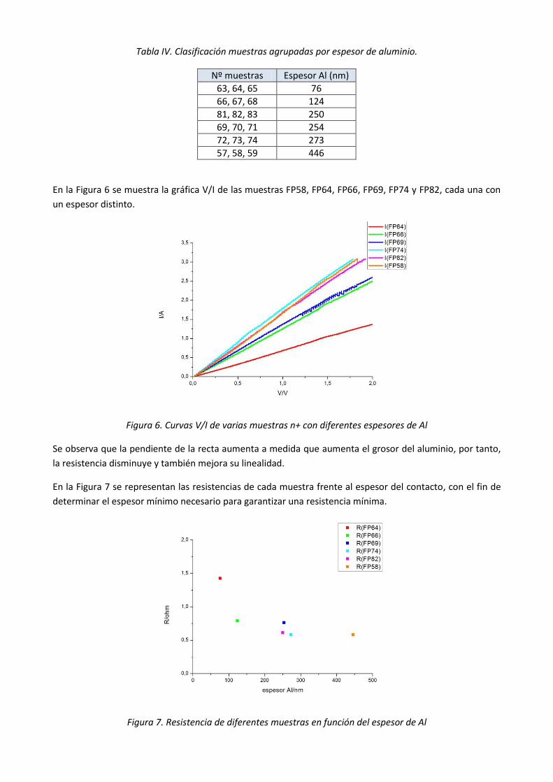
Tabla IV. Clasificación muestras agrupadas por espesor de aluminio.
Nº muestras Espesor Al (nm)
63, 64, 65 76
66, 67, 68 124
81, 82, 83 250
69, 70, 71 254
72, 73, 74 273
57, 58, 59 446
En la Figura 6 se muestra la gráfica V/I de las muestras FP58, FP64, FP66, FP69, FP74 y FP82, cada una con
un espesor distinto.
Figura 6. Curvas V/I de varias muestras n+ con diferentes espesores de Al
Se observa que la pendiente de la recta aumenta a medida que aumenta el grosor del aluminio, por tanto,
la resistencia disminuye y también mejora su linealidad.
En la Figura 7 se representan las resistencias de cada muestra frente al espesor del contacto, con el fin de
determinar el espesor mínimo necesario para garantizar una resistencia mínima.
Figura 7. Resistencia de diferentes muestras en función del espesor de Al
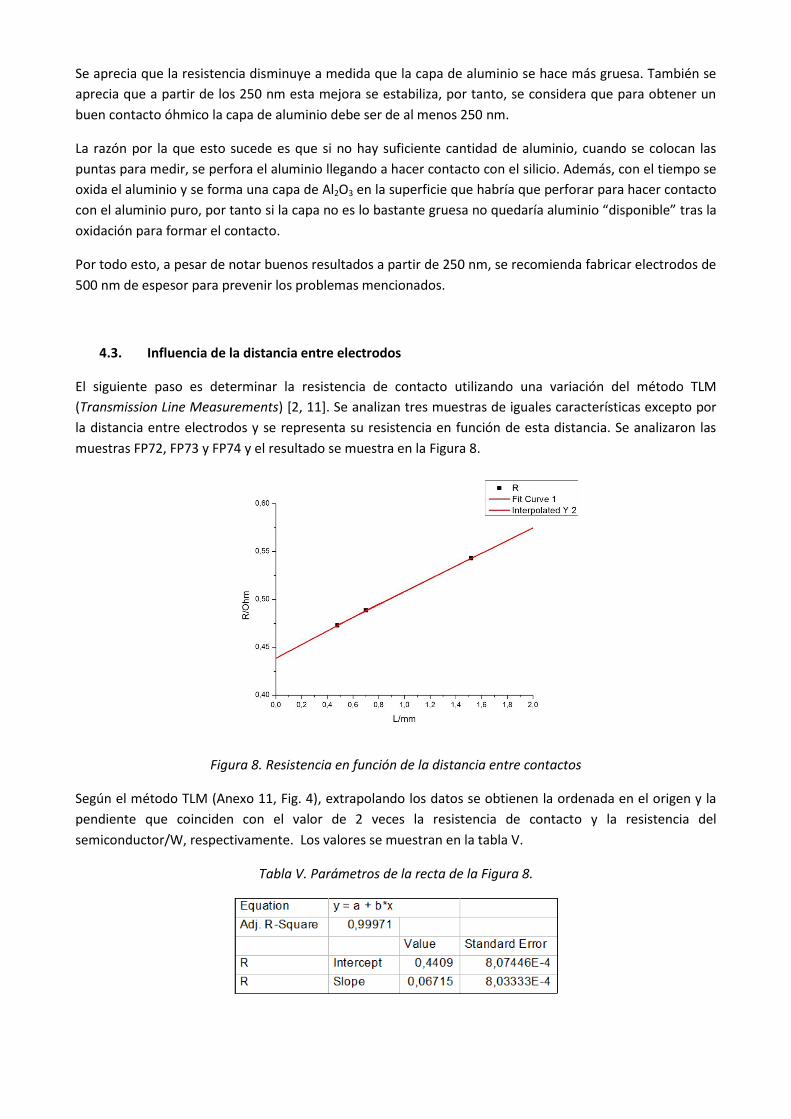
Se aprecia que la resistencia disminuye a medida que la capa de aluminio se hace más gruesa. También se
aprecia que a partir de los 250 nm esta mejora se estabiliza, por tanto, se considera que para obtener un
buen contacto óhmico la capa de aluminio debe ser de al menos 250 nm.
La razón por la que esto sucede es que si no hay suficiente cantidad de aluminio, cuando se colocan las
puntas para medir, se perfora el aluminio llegando a hacer contacto con el silicio. Además, con el tiempo se
oxida el aluminio y se forma una capa de Al2O3 en la superficie que habría que perforar para hacer contacto
con el aluminio puro, por tanto si la capa no es lo bastante gruesa no quedaría aluminio “disponible” tras la
oxidación para formar el contacto.
Por todo esto, a pesar de notar buenos resultados a partir de 250 nm, se recomienda fabricar electrodos de
500 nm de espesor para prevenir los problemas mencionados.
4.3. Influencia de la distancia entre electrodos
El siguiente paso es determinar la resistencia de contacto utilizando una variación del método TLM
(Transmission Line Measurements) [2, 11]. Se analizan tres muestras de iguales características excepto por
la distancia entre electrodos y se representa su resistencia en función de esta distancia. Se analizaron las
muestras FP72, FP73 y FP74 y el resultado se muestra en la Figura 8.
Figura 8. Resistencia en función de la distancia entre contactos
Según el método TLM (Anexo 11, Fig. 4), extrapolando los datos se obtienen la ordenada en el origen y la
pendiente que coinciden con el valor de 2 veces la resistencia de contacto y la resistencia del
semiconductor/W, respectivamente. Los valores se muestran en la tabla V.
Tabla V. Parámetros de la recta de la Figura 8.

Por tanto, se obtiene que el valor de RC es 0,22 Ω y la resistencia del semiconductor es Rsemi = 2.01×10⁻⁴ Ω,
lo cual coincide con lo esperado, ya que las especificaciones de la oblea dicen que la resistividad es <0,005
Ω.cm. El valor de la resistencia de contacto es lo suficientemente bajo para considerar que el contacto es
óhmico.
4.4. Influencia del recocido
El último paso para optimizar los contactos óhmicos es someterlos al recocido y comprobar que la
resistencia de contacto mejora tras el calentamiento.
Se ha sometido la muestra FP89 a un recocido durante 1 hora a 250 C en atmósfera de argón y los valores
de resistencia antes y después del proceso se muestran en la Figura 9.
Figura 9. Resistencia de una muestra antes y después del recocido térmico.
En la gráfica de la Figura 9 se observa claramente como la resistencia disminuye y gana linealidad,
posiblemente debido a la disolución del óxido nativo de silicio entre la superficie de éste y el aluminio, así
como al spiking que mejora la interfase, tal como se comentó en el apartado 3.4 [6, 16].
5. Conclusiones
Tras la realización de este trabajo se han logrado los objetivos propuestos:
- Se ha comprobado que es necesario utilizar un sustrato altamente dopado, de al menos 1019
átomos/cm-3 para tener contacto óhmico.
- Se ha investigado que el contacto mejora cuando la capa de aluminio que se deposita sobre el
silicio es mayor de 250 nm y se recomienda para posteriores trabajos realizar contactos de 500 nm
de espesor para asegurar un buen contacto.
- Se han caracterizado los contactos fabricados tanto físicamente, con la técnica de perfilometría,
como eléctricamente, con las curvas V-I.
- Se calcula la resistencia de contacto usando el método TLM y se obtiene un valor de 0,22 Ω.
- Se han aprendido y utilizado varias técnicas de fabricación microelectrónica, además de mejorar y
actualizar los protocolos de trabajo dentro de la sala blanca.
- Se han puesto en práctica, y mejorado en la medida de lo posible, los procedimientos para fabricar
contactos óhmicos.
En resumen, se ha logrado el objetivo, que era demostrar que es posible fabricar contactos óhmicos y
caracterizarlos; así como demostrar que las técnicas sobre tratamiento de obleas de silicio, fabricación de
dispositivos y caracterización funcionan con materiales conocidos, como el silicio.
Esto es importante de cara a iniciar una serie de pasos, que a largo plazo están encaminados a
experimentar con nuevos materiales como aleaciones de GeSn para dispositivos microelectrónicos más
rápidos y circuitos integrados fotónicos (PICs del inglés Photonic Integrated Circuits).
6. Bibliografía
6.1. Obras citadas
[1] Albella Marín, José María et al. Fundamentos de microelectrónica, nanoelectrónica y fotónica.
Madrid: Pearson Educación, 2005.
[2] Doolittle, Adam. “Semiconductor Device and Material Characterization”. Georgia Tech: Shcool of
Electrical and Computer Engineering. 2017. Web. 21 May. 2017.
[3] Fong, Kean Chern et al. “Contact Resistivity of Evaporated Al Contacts for Silicon Solar Cells”. IEEE
Journal of Photovoltaics. Sep. 2015 (5). 1304 – 1309.
[4] Frutos, Jorge y Miguel Ruiz. “Los nuevos cambios en ISO 14644-1”. Pharmatec. Ene. – Feb. 2016
(20). 90 – 95.
[5] Northrop, D. C. y C. Puddy. “Ohmic Contacts Between Evaporated Aluminium and n-Type Silicon”.
Nuclear Instruments and Methods. North-Holland Publishing Co. 1971 (94). 557 – 559.
[6] Saraswat, Krishna C. “Metal/Semiconductor Ohmic Contacts”. EE311. Stanford University. May.
2006. Web. 10 Jun. 2017.
[7] Sarmiento Arellano, J. “Fabricación, análisis experimental y caracterización de contactos Óhmicos y
Schottky”. Puebla, México: Benemérita Universidad Autónoma de Puebla. Trabajo de Fin de Máster.
[8] Stange, Daniela et al. "Optically Pumped GeSn Microdisk Lasers on Si". ACS Photonics. 24 Jun. 2016
(3). 1279 – 1285.
[9] Stefanov, Stefan et al. "Silicon germanium tin alloys formed by pulsed laser induced
epitaxy". Applied Physics Letters. 14 May. 2012. Web.
[10] Stefanov, Stefan et al. "Structure and composition of Silicon–Germanium–Tin microstructures
obtained through Mask Projection assisted Pulsed Laser Induced Epitaxy". Microelectronic Engineering.
2014 (100). 18 – 21.
[11] Tuttle, Gary. Semiconductor Fabrication. 26 Mar. 2017. Web. 01 Jun. 2017.

[12] Uemura, Eiichi, Hiroshi Onoda y Shoji Madokoro. “High Reliable A1-Si Alloy/Si Contacts by Rapid
Thermal Sintering”. 26th annual proceedings reliability physics. Nueva York: Institute of Electrical and
Electronics Engineers, 1988. 230 – 233.
[13] Wirths, S. et al. "Lasing in direct-bandgap GeSn alloy grown on Si". Nature Photonics. 13 Ene. 2015.
Web.
[14] Wirths, S. et al. "Tensely strained GeSn alloys as optical gain media". Applied Physics Letters. 7 Nov.
2013. Web.
[15] Yu, A. Y. C. “Electron Tunneling and Contact Resistance of Metal-Silicon Contact Barriers”. Solid-
State Electronics. 1970 (13). 239 – 247.
[16] Van Zeghbroeck, B. “Principles of Semiconductor Devices”. Principles of Electronic Devices. 2011.
Web. 15 May. 2017.
6.2. Obras consultadas
Berger, H. H. “Contact Resistance and Contact Resistivity”. Solid-State Science and Technlogy. Abr. 1972
(119). 507 – 514.
Card, Howard C. “Aluminum-Silicon Schottky barriers and Ohmic Contacts in Integrated Circuits”. IEEE
Transactions on Electron Devices. Jun. 1976 (23). 538 – 544.
Chang, C. Y. y K. Fang. “Specific Contact Resistance of Metal-Semiconductor Barriers”. Solid-State
Electronics. 1971 (14). 541 – 550.
Cohen, Simon S. “Contact Resistance and Methods for its Determination”. Thin Solid Films. 1983 (104).
361 – 379.
Galvez, P. et al. “Monitorización de partículas de una sala blanca: requerimientos normativos en
terapias avanzadas”. Universidad de Granada. 19 Jul. 2010. Web. 21 May. 2017.
Halperin, L. E. et al. “Silicon Schottky Barriers and p-n Junctions with Highly Stable Aluminum Contact
Metallization”. IEEE Electron Device Letters. Jun. 1991 (12). 309 – 311.
Katkhouda, Kamal et al. “Quick Determination of Specific Contact Resistance of Metal–Semiconductor
Point Contacts on Highly Doped Silicon”. IEEE Journal of Photovoltaics. Ene. 2015 (5). 299 – 306.
Loh, William M. et al. “Modeling and Measurement of Contact Resistances”. IEEE Transactions on
Electron Devices. Mar. 1987 (34). 512 – 524.
Lou, Yung-Song y Ching-Yuan Wu. “A Self-Consistent Characterization Methodology for Schottky-Barrier
Diodes and Ohmic Contacts”. IEEE Transactions on Electron Devices. Abr. 1994 (41). 558 – 566.
Onoda, Hiroshi. “Dependence of Al-Si/Si Contact Resistance on Substrate Surface Orientation”. IEEE
Electron Device Letters. Nov. 1988 (9). 613 – 615.
Pierret, Robert F. Fundamentos de semiconductores. Wilmington: Addison-Wesley Iberoamericana,
1994.
Piotrowska, A., A. Guivarch y G. Pelous. “Ohmic Contacts to III-V Compound Semiconductors: A Review
of Fabrication Techniques”. Solid-State Electronics. 1983 (26). 179 – 197.

Rideout, V. L. “A Review of the Theory and Technology for Ohmic Contacts to Group III-V Compound
Semiconductors”. Solid-State Electronics. 1975 (18). 541 – 550.
Sze, S. M. y Ng Kwok K. Physics of Semiconductor Devices. Nueva York: John Wiley & Sons, 2006.
Turners, M. J. y E. H. Rhodbrick. “Metal-Silicon Schottky Barriers”. Solid-State Electronics. 1968 (11). 291
– 300.

Anexo 1: Marco teórico
Para explicar el comportamiento de los contactos metal-semiconductor a nivel físico, hay que remontarse
al modelo de bandas de energía.
En los metales, al contrario que los semiconductores, las bandas de conducción y valencia se solapan en
una única banda, con el nivel de Fermi en el interior de ella. Esto quiere decir que una gran proporción de
los electrones están en las proximidades de este nivel, según se aprecia en la función de distribución n(E)
de la Figura 1.1. Por esto, y porque la banda de conducción de los metales suele ser bastante ancha, se
suele representar sólo el nivel de Fermi, (Ef)m , en el diagrama de energía de los metales.
Para el caso de los semiconductores, se representan las bandas de valencia, Ev, y conducción, Ec, con el
nivel de Fermi, (Ef)s, entre ambas, en la llamada banda prohibida, Eg, que en el caso del silicio tiene un valor
de 1.12 eV a temperatura ambiente (300K). Si el semiconductor es tipo n el nivel de Fermi está más
próximo a la banda de conducción, como en la Figura 1.1; mientras que si es tipo p, se aproxima a la banda
de valencia.
Figura 1.1. Diagrama de bandas de energía de un metal y un semiconductor tipo n, antes de entrar en
contacto.
Para poder establecer una comparación entre los niveles de energía de metales y semiconductores, se
necesita de un nivel de referencia. Habitualmente se toma el nivel de vacío, Evac, que es la energía de un
electrón en estado de reposo y alejado de la influencia de los átomos del material de procedencia.
La función de trabajo, qφm para el metal, y qφs para el semiconductor, se define como la energía necesaria
para liberar un electrón situado en el nivel de Fermi a un punto del vacío. Para los semiconductores es
necesario definir otro concepto, la afinidad electrónica, qχ, ya que normalmente no existen electrones en el
nivel de Fermi sino en el fondo de la banda de conducción. Por tanto, la afinidad electrónica es la energía
necesaria para trasladar un electrón desde la parte inferior de la banda de conducción al vacío. Tanto la
función de trabajo como la afinidad electrónica son magnitudes intrínsecas del material.
En la tabla I.I se encuentran los valores típicos de la función de trabajo de algunos metales y en la tabla I.II,
los valores de afinidad electrónica de los semiconductores más utilizados.
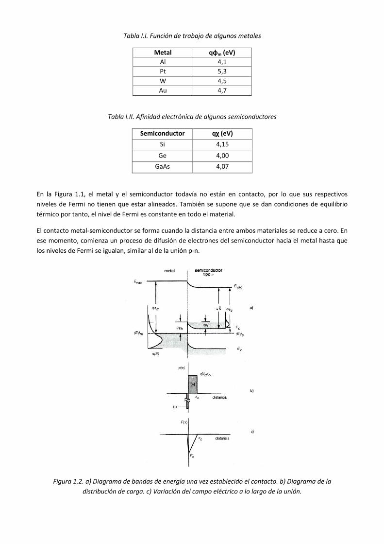
Tabla I.I. Función de trabajo de algunos metales
Metal qφm (eV)
Al 4,1
Pt 5,3
W 4,5
Au 4,7
Tabla I.II. Afinidad electrónica de algunos semiconductores
Semiconductor qχ (eV)
Si 4,15
Ge 4,00
GaAs 4,07
En la Figura 1.1, el metal y el semiconductor todavía no están en contacto, por lo que sus respectivos
niveles de Fermi no tienen que estar alineados. También se supone que se dan condiciones de equilibrio
térmico por tanto, el nivel de Fermi es constante en todo el material.
El contacto metal-semiconductor se forma cuando la distancia entre ambos materiales se reduce a cero. En
ese momento, comienza un proceso de difusión de electrones del semiconductor hacia el metal hasta que
los niveles de Fermi se igualan, similar al de la unión p-n.
Figura 1.2. a) Diagrama de bandas de energía una vez establecido el contacto. b) Diagrama de la
distribución de carga. c) Variación del campo eléctrico a lo largo de la unión.
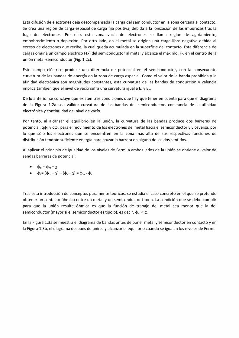
Esta difusión de electrones deja descompensada la carga del semiconductor en la zona cercana al contacto.
Se crea una región de carga espacial de carga fija positiva, debida a la ionización de las impurezas tras la
fuga de electrones. Por ello, esta zona vacía de electrones se llama región de agotamiento,
empobrecimiento o deplexión. Por otro lado, en el metal se origina una carga libre negativa debida al
exceso de electrones que recibe, la cual queda acumulada en la superficie del contacto. Esta diferencia de
cargas origina un campo eléctrico F(x) del semiconductor al metal y alcanza el máximo, F0, en el centro de la
unión metal-semiconductor (Fig. 1.2c).
Este campo eléctrico produce una diferencia de potencial en el semiconductor, con la consecuente
curvatura de las bandas de energía en la zona de carga espacial. Como el valor de la banda prohibida y la
afinidad electrónica son magnitudes constantes, esta curvatura de las bandas de conducción y valencia
implica también que el nivel de vacío sufra una curvatura igual a Ec y Ev.
De lo anterior se concluye que existen tres condiciones que hay que tener en cuenta para que el diagrama
de la Figura 1.2a sea válido: curvatura de las bandas del semiconductor, constancia de la afinidad
electrónica y continuidad del nivel de vacío.
Por tanto, al alcanzar el equilibrio en la unión, la curvatura de las bandas produce dos barreras de
potencial, qφb y qφi, para el movimiento de los electrones del metal hacia el semiconductor y viceversa, por
lo que sólo los electrones que se encuentren en la zona más alta de sus respectivas funciones de
distribución tendrán suficiente energía para cruzar la barrera en alguno de los dos sentidos.
Al aplicar el principio de igualdad de los niveles de Fermi a ambos lados de la unión se obtiene el valor de
sendas barreras de potencial:
φb = φm – χ
φi = (φm – χ) – (φs – χ) = φm - φs
Tras esta introducción de conceptos puramente teóricos, se estudia el caso concreto en el que se pretende
obtener un contacto óhmico entre un metal y un semiconductor tipo n. La condición que se debe cumplir
para que la unión resulte óhmica es que la función de trabajo del metal sea menor que la del
semiconductor (mayor si el semiconductor es tipo p), es decir, φm < φs.
En la Figura 1.3a se muestra el diagrama de bandas antes de poner metal y semiconductor en contacto y en
la Figura 1.3b, el diagrama después de unirse y alcanzar el equilibrio cuando se igualan los niveles de Fermi.

Figura 1.3. Diagrama de bandas entre un metal y un semiconductor tipo n, a) antes de entrar en contacto.
b) después de entrar en contacto.
En este caso, como los electrones del metal tienen más energía que los del semiconductor, el flujo de
electrones se produce en sentido contrario al caso de la figura 1.2a y por tanto, el campo eléctrico se dirige
del metal al semiconductor.
Siguiendo el razonamiento anterior, ahora la carga fija positiva se encuentra del lado del metal y la carga
libre del semiconductor. Esta última se distribuye en una capa muy fina llamada capa de acumulación. Por
tanto, las bandas de energía en el semiconductor ahora se curvan hacia arriba en una zona muy estrecha
formando una pequeña barrera al pasar del nivel de Fermi del metal a la banda de conducción del
semiconductor, que se calcula como q(φs – χ) según la Figura 1.3b.
Por último, hay que resaltar que durante el movimiento de electrones en ambos sentidos no se encuentra
barrera de potencial y que existe una gran concentración de electrones con energía suficiente para cruzar la
barrera, con lo que la resistencia de contacto es despreciable. Cuando esto sucede se dice que el contacto
es óhmico.
Anexo 2: Estado del arte
A lo largo de la última década han cobrado importancia los descubrimientos relacionados con la posibilidad
de obtener dispositivos micro- y optoelectrónicos compatibles con tecnología CMOS, basándose
únicamente en elementos del Grupo IV (Si, Ge, Sn) a pesar de que los primeros dos sean de gap indirecto y,
por tanto, teóricamente son poco eficientes como emisores de luz.
Sin embargo, se ha descubierto que la aleación de Germanio-Estaño sobre Silicio cristalino con interfase de
Germanio, GeSn/Ge/Si(100) tiene gap directo, lo que supone una revolución a nivel científico, ya que las
limitaciones físicas de los elementos de gap indirecto se superan satisfactoriamente y es posible realizar
emisores luz. Esto genera un impacto social y económico, debido a que se podrán reducir costes al utilizar
estos materiales en lugar de los elementos de los Grupos III/V y se podrán fabricar emisores de luz (LEDs,
láser) sobre obleas convencionales de silicio (Si-onChip), abriendo las puertas a la obtención de circuitos
integrados fotónicos (PICs) y Biosensores para LabOnChip.
Para profundizar sobre las investigaciones en curso en este campo se puede acudir a las publicaciones del
Grupo de Nuevos Materiales del Departamento de Física Aplicada de la Escuela de Ingeniería Industrial de
la Universidad de Vigo, citadas en la bibliografía de este trabajo y disponibles online [8, 9, 10, 13, 14].
Este proyecto está situado en el marco de dichas investigaciones dado que permite comprobar la
adecuación de las técnicas de producción microelectrónica conocidas sobre materiales ampliamente
utilizados como el Silicio para, posteriormente, sentar las bases de futuros proyectos que en última
instancia permitan experimentar con la aleación de GeSn.

Anexo 3: Sala blanca
Una sala blanca debe tener ciertos parámetros ambientales controlados, como la humedad, la temperatura
y las partículas en suspensión y estar específicamente diseñada y construida para minimizar la introducción,
generación y retención de partículas en su interior. Según la Federal Standard 209 se define como: “Una
habitación donde la concentración de partículas en el aire está controlada y donde existen una o más zonas
limpias". En ISO 14644-1 (“Sala limpia y entornos controlados asociados - Parte 1: Clasificación de la
limpieza del aire”) una sala blanca se define como “Una habitación en la que la concentración de partículas
en el aire está controlada y la cual es construida y utilizada de modo que se minimice la introducción,
generación y retención de partículas en su interior y en la que otros parámetros relevantes (por ejemplo
temperatura, humedad o presión) están debidamente controlados”.
Para mantener unos niveles de concentración de partículas en el aire dentro de unos límites especificados,
se aplican cuatro reglas fundamentales:
1. Se debe evitar introducir contaminación del exterior.
2. Los equipos y herramientas dentro del entorno controlado no deben generar contaminantes que
entren en contacto con la atmósfera, por ejemplo, como resultado de reacciones químicas,
procesos biológicos o físicos.
3. La contaminación no se puede acumular dentro de la sala.
4. La contaminación existente debe eliminarse en la mayor medida posible y tan rápido como se
pueda.
El nivel de contaminación en el aire depende en gran medida de las actividades que generan partículas en
la estancia, particularmente del personal que trabaja en ella, quien también (y sobre todo) contribuye a
incrementar los niveles de contaminación. Existen cinco fuentes básicas de contaminación:
1. Las propias instalaciones (paredes, suelo, pintura, etc.).
2. Personas (escamas de piel, grasa, pelo, perfumes, cosméticos, etc.).
3. Herramientas (lubricantes, emisiones, escobas, etc.).
4. Fluidos (partículas en suspensión en el aire, bacterias, microorganismos, etc.).
5. El propio producto fabricado/manipulado (dispositivos de silicio, partículas de aluminio, etc.).
Las características básicas que describen una sala blanca son, entre otras, las siguientes:
1. El aire que entra es filtrado para dejarlo libre de microorganismos y partículas. Estos filtros están
continuamente en funcionamiento para renovar y mantener el aire siempre limpio en el interior de
la sala.
2. Es una sala sobrepresurizada, es decir, con una presión ligeramente superior a la del exterior para
así evitar que, en caso de que las puertas se abran, no entre el aire con impurezas del exterior.
3. Está equipada con filtros HEPA o ULPA repartidos por diferentes zonas de la habitación para
capturar partículas y devolver el aire limpio a la sala.
4. Los trabajadores deben utilizar un vestuario específico que no desprenda partículas, el cual no debe
salir de la sala para evitar la contaminación del exterior. Este vestuario se renueva periódicamente,
y está formado principalmente por bata, gorro, calzas o cubrezapatos, guantes, mascarilla y gafas
de protección. En salas de muy alto índice de pureza se necesita utilizar un mono integral en lugar
de la bata y un verdugo que cubra cabeza y hombros.
5. Posee una zona limpia y otra zona de “vestuario”, que están separadas por cortinas, alfombras
adhesivas u otros elementos para poder delimitar la zona.

6. Predominan las esquinas redondeadas para evitar la acumulación de polvo, paredes, suelo y techo
fabricados en materiales específicamente diseñados para salas blancas
3.1. Clasificación
Una sala blanca se clasifica en función de dos criterios: el flujo de aire y la concentración de partículas en
suspensión.
Según la forma en que se distribuye el flujo de aire en su interior, puede ser de:
- Flujo multidireccional o turbulento: el aire entra a la sala por uno o diversos puntos y es aspirado
en otro punto enfrentado al de entrada. El aire entre la entrada y la salida sigue una trayectoria
incontrolada y variable. El aire se mantiene en movimiento constante pero no todo en la misma
dirección, por ello, con este tipo de flujo es imposible evitar la contaminación cruzada y la única
forma de asegurar la calidad del aire es la constante renovación del aire. De este tipo es la sala
blanca que se usó para realizar este TFG.
- Flujo unidireccional o laminar: el aire entra en la sala a través de una superficie vertical u horizontal
a una velocidad constante (0.45m/s±20% según ISO 14644-1) y es expulsado por otra superficie
opuesta a la de entrada. El aire recorre la sala uniformemente realizando un barrido continuo con
efecto pistón. De esta forma, la trayectoria del aire se predice con una exactitud bastante buena y
se garantiza la no contaminación cruzada del producto a pesar de que la presencia de
equipamiento, mobiliario y operarios pueda generar pequeñas turbulencias. En la sala blanca que
se utilizó para realizar este TFG existen varias zonas de este tipo como por ejemplo la campana en
las cuales se marcó, limpió y manipuló las muestras y las máscaras antes de depositar los
electrodos.
Según el número y tamaño de las partículas permitidas por volumen de aire existen diversos estándares.
Uno de ellos es el estándar FED STD 209E (Fig. 3.1) que fue cancelado oficialmente en 2001, aunque todavía
sigue siendo utilizado.
Figura 3.1. Estándar FED STD 209E
Las clases se denominan con números (“1”, “100”, “100000”...) los cuales representan la cantidad máxima
de partículas de 0,5 µm o superior permitida por pie cúbico de aire, esto es, una sala blanca de clase 100
tendrá como máximo 100 partículas por pie cúbico de tamaño 0.5 µm o mayor.

Sin embargo, actualmente se utiliza más la norma ISO 14644 (Fig 3.2), la cual establece una clasificación por
niveles de limpieza del aire en salas blancas y entornos controlados asociados. En 2005 fue revisada y
actualizada, introduciendo algunas novedades, como la posibilidad de establecer clasificaciones
intermedias (por ejemplo se contempla la posibilidad de tener una sala blanca de clase 4.8). También se
define el método estándar de muestreo y el procedimiento para hacer las medidas que determinen la
concentración de partículas en el aire. Las medidas se realizan con unos medidores o contadores de
partículas, que se van colocando por la sala y aspiran aire por un tubo para posteriormente contabilizar las
partículas presentes en él. El número de puntos de medida y su separación entre ellos también se
actualizaron en la revisión de la mencionada norma ISO [4].
Imagen 3.2. ISO 14644-1. Revisión 2015
3.2. Protocolo de limpieza y mantenimiento
Mantener la sala blanca dentro de los niveles de contaminación adecuados requiere realizar
periódicamente limpiezas generales así como un correcto mantenimiento de las instalaciones para que la
sala se mantenga en las mejores condiciones hasta la siguiente limpieza.
La limpieza debe llevarla a cabo personal con conocimientos sobre los requisitos de una sala blanca. Hay
que tener en cuenta una serie de consideraciones al respecto:
1. El orden de limpieza sería empezando por el techo, lámparas, paredes, puertas y marcos y
ventanas, siempre hacia abajo. Así las partículas que se desprendan terminarán en el suelo, de
donde serán eliminadas al final del proceso.
2. Se utilizan materiales específicos para la limpieza de salas blancas, como paños de microfibra,
fregonas o esponjas especiales que no dejan residuos.
3. En general, la limpieza se hace empezando por las zonas con un nivel más crítico de limpieza,
repitiendo el proceso cada vez con el material adecuado para retirar la suciedad más pequeña.
4. Los agentes de limpieza que se utilizan son agua y jabón para la suciedad más gruesa y etanol para
el acabado final.
5. Se combina el uso de la aspiradora con la pistola de nitrógeno o spray de aire a presión para
eliminar polvo de las superficies más inaccesibles.

El mantenimiento básico consiste en llevar en todo momento la ropa adecuada para el trabajo en sala
blanca, un equipamiento compuesto de bata o mono, gorro, calzas o cubrezapatos, guantes, mascarilla y en
ocasiones donde se requiera una mayor protección polainas y verdugo; y mantener la sala
sobrepresurizada.
3.3. Control de partículas
Para saber a qué nivel de la clasificación ISO 14644 pertenece la sala blanca y sus diferentes zonas de
trabajo en la cual se realizó este TFG, y también para llevar un control del estado de la sala, se realizan
periódicamente medidas del nivel de partículas presentes en el aire utilizando un aparato portátil llamado
medidor o contador de partículas. En este caso, el instrumento utilizado es el HANDHELD 3016 de
Lighthouse Worldwide Solutions.
El funcionamiento del medidor consiste en aspirar aire por el tubo metálico de toma de muestra y
contabilizar el número de partículas de diferentes tamaños (de 0,3 µm a 10 µm) en 1 m3 de volumen de aire
aspirado. El instrumento utiliza una fuente de luz láser de diodo y óptica de captación para la detección de
partículas. Las partículas dispersan la luz del diodo láser y la óptica de recolección recoge y concentra la luz
sobre un fotodiodo que convierte las ráfagas de luz en impulsos eléctricos. La altura de pulso es una
medida de tamaño de partícula. Los pulsos son contados y su amplitud se mide para determinar el tamaño
de partícula. Los resultados se muestran como recuentos de partículas en el canal de tamaño especificado.
En los Anexos 10 y 11 se incluyen los procedimientos normalizados de trabajo relativos al control de
partículas.

Anexo 4: Cutting and marking silicon, germanium, quartz and glass Substrates
4.1. Objective The aim of this document is to explain the procedure to cut and mark silicon (Si), germanium (Ge) and
quartz (SiO2) or glass substrates or wafers.
4.2. Scope
This procedure applies to silicon, germanium and quartz or glass substrates that are used in the FA3
laboratories of the Department of Applied Physics.
4.3. References
Not specified.
4.4. Generalities
Silicon, germanium and quartz or glass substrates/wafers are used as substrates to be coated with thin
films in order to analyze the deposited coatings through different characterization techniques, to process
them further by conventional or laser techniques (ELA, PLIE) or to use in microelectronic, photonic or
biomedical devices.
4.5. Materials
4.5.1. Instruments
Diamond-tipped PROXXON engraver.
Diamond-tipped pen, pliers to break the wafers.
Clean room tissue, plastic gloves.
Ruler, permanent universal pen (Staedler).
Teflon tweezers to avoid metal contamination.
4.5.2. Products
Si, Ge Quartz or glass wafer/substrates.
4.6. Safety Warnings
Use gloves and be careful to avoid sharp splinters.
Avoid manipulations of samples and wafer with bare hands and their contamination with greases.
Use Teflon tweezers to avoid metal contamination.
4.7. Procedure
Put on gloves to avoid contaminating the sample with hands fat, and put laboratory tissue on the table to
perform the cutting and marking of the wafers on top of them. Prepare all the other required stuff. In the
pictures we see the diamond-tipped PROXXON engraver, a diamond-tipped pen and the black pliers used to
precisely break the wafers along the crystal axis or the line marked with the diamond pen.

4.7.1. Cutting
Take the wafer out of the box using the tweezers and place it on the laboratory tissue.
Flip the wafer to work on the side with the rough surface.
If you want to achieve rectangular shapes you must make measures taking references. At the end of this procedure you will find a template for cutting Si wafers of different sizes. Use a ruler to measure the samples of the desired size. Take as reference the axis formed by the flat side of the wafer (110 axis for Si(100) wafers). Mark the dimensions of the shape with the permanent pen.
Once the desired dimensions are defined, the cutting can be done in 2 different ways: The easiest way is to draw a continuous line with the diamond-tipped pen and use the
black pliers to break the wafer aligning its white line marked on the pliers with the one drawn with the diamond-tipped pen.
A very efficient way that needs more skills is to press with a very sharp diamond tip on one flat edge. The silicon sample will break following the crystal plane starting at this point and
can be perfect, if the wafer is thin. However, for thicker wafers (>100 m) the breaking edge might split and follow another crystallographic plane. Note that if you use this method starting a round edge, it might break following any crystal plane, making it hard to get rectangular samples.
Store the wafers that are not usable as samples in a plastic bag.
Detail of the white line on the pliers that has to be aligned and image of a cut wafer.
4.7.2. Marking
Before carrying out the cleaning process, samples must be identified. This is done using the diamond-tipped
PROXXON engraver.

Mark the samples by writing little identification characters on the lower right corner of the rough face (backside) of the sample, when aligning the flat to the bottom. This must be done pressing the engraver tip with moderate strength. If you press too softly, identification characters will be almost unrecognizable after cleaning the sample with HF. Pressing too much will increase the likelihood to break the wafer following a crystal plane.
Always leave a reference sample for comparing all processed samples with the original substrate. This sample will not be subjected to the cleaning process. Choose as reference sample, the smallest or the one with most imperfect cutting, but take a representative one (not form the border of the wafer) and store it in the samples box.
ATTENTION: Be careful when connecting the 3 tip cable of the PROXXON engraver as these tips can easily
break.
4.8. Revision history
Rev. Date Author Changes
0
1
2
11-07-2011
11-07-2012
I.García, S.Chiussi
M.Pérez, S.Chiussi
New equipment process optimization.
3 06-06-2016 J.L.Frieiro, M.Gómez, S.Chiussi New PNT format and equipment

Anexo 5: Cleaning of silicon, germanium and quartz substrates
5.1. Objective
The aim of this document is to explain the procedure to clean of silicon, germanium or quartz wafers,
removing organic and inorganic contaminations from the surface of wafers.
5.2. Scope
This procedure applies to silicon, germanium and quartz surfaces or wafers used in the FA3 laboratories of
the Department of Applied Physics.
5.3. References
Not specified.
5.4. Generalities
Silicon, germanium and quartz wafers are used at the LCVD laboratory as substrates to be coated and then
used in microelectronic, photonic or biomedical applications.
5.5. Materials
5.5.1. Instruments
Clean-room tissues
Ultrasonic bath.
Conductivity meter CM35+ (optional).
N2 (4.0 purity) dispensing gun.
Laminar flow box with hood.
Timer.
Teflon holder and tweezers to avoid metal contamination.
Several 250 ml plastic (for HF) and Pyrex (for Piranha and solvents) beakers.
1000 ml Pyrex beaker for waste disposal.
HV/UHV chamber for baking.
Appropriate containers for the generated waste.
5.5.2. Products
General cleaning of all substrates (Silicon, Germanium, Quartz): Acetone (spectroscopy grade) Ethanol, Isopropanol (absolute) Deionized (DI) water.
Specific cleaning processes: o Silicon and Quartz (Strictly forbidden for Germanium):
Piranha solution o Silicon (Strictly forbidden for Quartz and Germanium):
HF (8%) (40%HF/H20 1/5). o Germanium (Strictly forbidden for Quartz):
HF (0.4%) (40%HF/H20 1/100)
5.6. Safety Warnings
Use gloves and protective googles.
Avoid manipulations of samples and wafer with bare hands.
Always use Teflon tweezers.
Be particularly careful when handling HF. It is very dangerous for your health, because it is a neurotoxin and it removes Ca from your bones.

5.7. Procedure
Use gloves to avoid contaminating the sample with hands fat.
When drying with N2, apply the air always from above the sample holder to remove dust and water attached to the samples and avoid contamination of the next cleaning step.
5.7.1. General cleaning of all kind of substrates
Steps A) and B) can be omitted if it is guaranteed that the samples have no traces of fat. However, if you
are not sure, it is better to complete the entire cleaning procedure.
All the cleaning sub-processes with chemical substances must be done inside the flow box.
A) Ethanol and Acetone for removing oil, fats and inks.
For extremely dirty substrates or samples with photoresist.
Soak a clean-room tissue with ethanol and clean all the samples gently rubbing them. In this step and the following one, fat that can be on the sample’s surface should be removed or diluted.
Place the samples in the Teflon samples holder of the appropriate size and immerse it in a glass beaker with ethanol or the more aggressive acetone and in the ultrasonic bath for 5 minutes.
Remove the sample holder and rinse the samples with plenty of deionized water.
Immerse the sample holder in a beaker with approximately 150 ml deionized water.
Dry samples with N2.
Put it for about 30 s in the ultrasonic bath.
Rinse the samples again with plenty of deionized water and dry samples with N2.
Evaluate whether the ethanol or acetone can be reused in another application. If that is not possible pour it in the container of non-halogenated solvents.
B) Isopropanol for removing fats
Use for not extremely dirty substrates or those precleaned with acetone.
Place the Teflon sample holder in a glass beaker with Isopropanol and put it in the ultrasonic generator for 1 minute. This step is expected to remove remaining fats and water soluble contaminations that might dissolve better in Isopropanol than in acetone.
Rinse with plenty of deionized water.
Put it for about 30 seconds on the ultrasonic bath.
Rinse the samples again with plenty of deionized water.
Dry well with the N2 dispensing gun.
Evaluate whether the used isopropanol can be used for another application. If that is not possible drain it in the container of non-halogenated solvents.

5.7.2. Specific cleaning processes
Be careful during the following procedures because you will use extremely corrosive and toxic acids !
Carefully read PNTs P-017 and P-018 for preparation, use and disposal of these acids.
C) Piranha etching for Silicon and Quartz (Strictly forbidden for Germanium)
Immerse the Teflon sample holder in a plastic beaker containing the piranha solution (H2SO4: 30% H2O2 in proportion 3:1), be freshly prepared according to PNT P-017. Let it actuate for 10 minutes (the ultrasonic bath is not needed for this procedure).
After the 10 minutes, rinse the sample holder with plenty of deionized H2O, avoiding the contact of the solution with elements out of the Teflon beaker.
For a complete removal of the piranha solution, place the sample holder in 3 baths of deionized water for 5 minutes each, rinse with deionized water and dry with N2.
SiO2 surfaces (like native oxide and quartz) will now be free from organic contaminations and will be OH-terminated (hydroxylated).
D) HF (8%) etching for Si after Piranha cleaning (Strictly forbidden for Quartz and Germanium)
If you rinse a Si surface with native oxide or bulk SiO2, you can observe that the water drops remain stuck on the surface of the samples. This is due to the presence of hydrophilic SiO2 on the silicon wafer, which will be removed in the next steps
Immerse the sample holder in a plastic beaker with HF (8%) (40% HF : H2O; 1:5) according to PNT P-017 and place it in the ultrasonic bath for about 20 - 30s. o Complete removal of SiO2 can easily be checked looking at the sample surface, during
removal from HF solution and rinsing with deionized H2O. If there is still oxide (SiO2), the HF or H2O drops get stuck on the surface of the samples due to the hydrophilic SiO2 surface. When the SiO2 is completely removed (after 20 - 30s approximately), the surface gets hydrophobic and the drops slide immediately down. However, if the samples are immersed too long, the HF will continue to act and increase the roughness of the sample surface, thus hindering the HF or H2O drops to slide. Native SiO2 is etched with an approximate speed of 0.1 - 0.2 nm/s.
After having a clean SiO2 free surface, rinse the sample holder with plenty of deionized water.
For complete removal of the HF solution, place sample holder consecutively in 2 baths of deionized water for 1 minute each, then rinse with deionized water and dry with N2.
E) Further cleaning of Germanium, if desired, (Strictly forbidden for Quartz)
Cleaning of Ge surfaces is still an issue and there are very different recipes existing. This is due to the
poor stability of its oxide, leading to reproducibility and reliability issues. In contrast to silicon, the
nature and thickness of Ge “native” oxides are history dependent, and most phases of germanium
oxide are soluble in water.
In many groups the General cleaning procedures (A) is considered as sufficient (IHT) !
HF (0.4%) (IHP) o Immerse the sample holder in a plastic beaker with HF (0.4%) (40%HF/H20,
1/100) and place it in the ultrasonic bath for about 20 - 30s. o Rinse the sample holder with the samples with some deionized water. o For a complete removal of the HF solution, place the sample holder in 3 baths
with deionized water for 10 s each, rinse with deionized water and dry with N2.
HCl (10%) (Stanford) o Immerse the sample holder 10 min in a Pyrex beaker with 37% HCl : H2O in
proportion 1:3.7. This will produce a Cl terminated surface that should be smoother than the F terminated one.
o Rinse the sample holder with the samples with some deionized water.
5.7.3. Final cleaning for all kind of samples (optional)
Thermal annealing at 400C for 1 h in Ultra high vacuum (10-8 mbar) will finally evaporate residual H2O and produce desorption of H or Cl from H terminated Si and Ge as well as Cl terminated Ge surfaces.
5.8. Calculations and Uncertainties
Not considered.
5.9. Preliminary tests
A previous experiment has been performed, to determine the number of times needed to wash the silicon
samples, after HF cleaning, with deionized water. The aim was to evaluate how to perform wafer cleaning
as best as possible with the tools available in the laboratory. To do this, the electrical conductivity of the
water in the successive cleanings of the samples was measured with the CRISON conductivity meter
CM35+. The experiment was performed as follows.
Calibration of the CRISON conductivity meter CM35+ available in the laboratory.
Measurement of the different H2O available at the FA3 laboratory.
Deionized water (CACTI) EC 1.0
, Deionized water (petrol station) EC: 1.31
Distilled water EC: 1.98
This results show that the best water available for cleaning the silicon samples is the CACTI deionized
water, because it is the one with the lowest electrical conductivity value (1.0 ).
Therefore, to determine the number of beakers with CACTI deionized water needed in the last step of the
silicon samples cleaning, the electrical conductivity of each beaker used has been measured, with the aim
of reaching a value as close as possible to the value of pure deionized water of 1.0 . The experiment
has been performed as follows:
Cleaning the silicon samples with tissue soaked in Isopropanol.
Immersion for 30 s in 8% HF in the ultrasonic bath. o Successive rinsing in CACTI deionized water, and immersion on the beaker with deionized
water (250 ml approximately) in the ultrasonic bath (about 30s each time). Drying with N2 (purity 4.0) before each rinsing and subsequent immersion.
o Electrical conductivity measurement of the water in each beaker before and after the sample rinsing and immersion:
Measures of clean H2O before sample rinsing and immersion
B1: 1.03
B2: 1.02
B3: 1.03
B4: 1.01
B5: 0.99 It may be noted that in the last beakers the EC values decrease. This is because only two
beakers were used, replacing the deionized water always with new one, thus with each new
H2O fill, the beakers were cleaned too.
Measures of contaminated H2O after sample rinsing and immersion
B1: 785
B2: 1.38
B3: 1.20
B4: 1.15
B5: 1.02
From these results, it can be noted that the cleaning process has an exponential behavior.
There is a very sharp drop in conductivity, from the first beaker to the second, and then the
decrease is smoother. After the 5th beaker, an electrical conductivity value almost identical
to the one measured in the clean deionized water is obtained, thus the 5th beaker of the
cleaning procedure might be omitted.
5.10. Revision history
Rev. Date Author Changes
0
1
2
11-07-2011
11-07-2012
I.García
M.Pérez
Corrections considering the new equipment.
3 06-06-2016 J.L.Frieiro, M.Gómez,
S.Chiussi
Restructured and new PNT format, new etching
solutions, optimization of process.

Anexo 6: Preparation of a Piranha etching solution
6.1. Objective
The aim of this document is to explain the preparation of a piranha etching solution.
6.2. Scope
This procedure applies for the preparation of a piranha etching solution that consists in a mixture of
concentrated sulfuric acid (H2SO4) and 30% hydrogen peroxide (H2O2), at a 3:1 ratio.
6.3. References
Information related to this procedure:
https://en.wikipedia.org/wiki/Piranha_solution
http://www.lamp.umd.edu/Sop/Piranha_SOP.htm
http://web.mit.edu/cortiz/www/PiranhaSafety.doc
http://www.colorado.edu/ehs/pdf/piranha_disp.pdf
6.4. Generalities
Volume measurement does not need to be accurate since this solution will be employed for cleaning and
not for analytical purpose. Also, ratios for the solution may vary in a large range, according to different
protocols found in literature (see point 3).
Extreme caution is required when manipulating Piranha solution! Many things can cause the reaction to
accelerate and get out of control. "Out of control" can mean anything from the piranha foaming out of its
bin and on the desk; to an explosion with a huge shock wave including glove and acid-gown shredding glass
sharps. Piranha “burns” very efficiently organic compounds. If sufficient “fuel” is provided (i.e. photoresist),
huge quantities of heat and gas will be generated.
6.5. Materials
6.5.1. Tools
Laminar flow fume hood
Lab coat, latex gloves, protective goggles.
Pyrex glass beakers:
50 ml for measuring H2O2 volume.
100 ml or 250 ml, depending on needed quantity.
1000 ml for disposal (neutralizing with NaHCO3 and H2O) the mix
Teflon "beaker" as overfill protection
6.5.2. Products
Concentrated sulfuric acid (H2SO4).
Hydrogen peroxide 30%.
6.5.3. Other materials
NaHCO3 and H2O for neutralizing disposals.
pH paper for confirming neutralization of acid solution.
6.6. Safety Warnings
The sulfuric acid is a highly corrosive acid that can cause severe burns. Keep in mind that H2SO4 is strongly
hydroscopic and requires H2O to produce the acidic H3O+ ions.

Extreme caution is required when manipulating Piranha solution because it can explode if in contact with
excessive quantities of bases or organic material!
6.7. Procedure
Keep the Pyrex glass beakers with the solution always inside the Teflon beaker.
6.7.1. Preparation of 40 ml
First of all, add 30 ml sulfuric acid to the 100 ml glass beaker and then slowly fill it up to 40ml with
hydrogen peroxide 30%.
Wait until it cools down and stops producing vapor before using it (around 4-5minutes).
6.7.2. Preparation of 120 ml
Measure with a 100 ml Pyrex beaker 90 ml H2SO4, pour the sulfuric acid into the 250 ml glass beaker and
then slowly add 30ml of hydrogen peroxide 30%, using again the 100 ml beaker for measuring the
volume.
Wait until it cools down and stops producing vapor before using it (around 4-5minutes).
6.7.3. Dismissing excess and old solutions
Once the solution has been used it should not be mixed with other chemicals or disposed without
precautions, as the solution is highly reactive. For a proper disposal it has to be neutralized.
Because the Piranha solution is a very strong acid, it will be mixed with a basic substance such as
NaHCO3 (see sections 8 and 9 for the calculations of the quantities needed). The process is done in the
labs larger water sink as follows, since the produced gas is just CO2:
1. Add a spoon (the 200 ml plastic one in the 25 kg NaHCO3 container) of NaHCO3 into the big 1000 ml Pyrex glass beaker.
2. Add carefully some drops of the piranha solution, letting it settle until it stops bubbling and continue adding small quantities, always avoiding that bubbles or splashing H2SO4 exit the beaker.
3. Slowly pour some water into the beaker and mix with a glass bar to produce the required additional H3O
+ ions that will react with the NaHCO3. 4. Repeat steps 3 and 4 until disposing the complete Piranha solution. 5. Use water in excess to ensure that the reaction fully takes place. Check with the pH indicator
paper when the solution is neutralized. 6. Once it's neutralized, leave the solution in the beaker until the next day to ensure that the
solution reacted completely.
6.8. Calculations and Uncertainties
The reaction that takes place is:
2NaHCO3(s) + H2SO4(aq) → Na2SO4(aq) + 2CO2(g) + 2H2O
90 ml of H2SO4:
90 ml of H2SO4, with molecular weight of 98 g/mol and density of 1.84 g/cm3 corresponds to
(90 ml 1.84 g/cm3) / (98 g/mol) = 1.69 mol H2SO4

Since 2 H atoms / H2SO4 molecule are provided, 2 mol NaHCO3 are needed to neutralize 1 mol H2SO4, thus
requiring (2 mol 84 g/mol) = 168 g of NaHCO3 + sufficient H2O to hydrolyse the molecules and produce
H3O+ as well as Na2SO4(aq).
30 ml of 30% H2O2:
Since 30% H2O2 consumes NaHCO3 according to:
NaHCO3 + H2O2 Na2CO3 + H2O + CO2
The amount of used H2O2 with molecular weight of 34.02 g/mol and density of 1.11 g/cm3 is
(9 ml 1.11 g/cm3) / (34.02 g/mol) = 0.29 mol H2O2, thus requiring (0.29 mol 84 g/mol) = 24 g of NaHCO3.
90 ml of H2SO4 + 30 ml of 30% H2O2 (i.e. 120 ml Piranha solution):
Total amount of NaHCO3 required to neutralize a 120 ml Piranha mixture is therefore
168 g + 24 g = 192 g NaHCO3 + sufficient H2O to hydrolyse the molecules and produce H3O+ as well as
Na2SO4(aq).
Note that during the reaction the H2SO4 is dissolved in water. This is why water is used in the process of
neutralization since the acid is originally concentrated and not dissolved. However, always check carefully
that you do not need additional NaHCO3, or add additional NaHCO3 for security reasons.
6.9. Examples
For any other quantity of Piranha solution, it will be needed:
(192 g NaHCO3) / (120 ml Piranha solution) = 1.6 g of NaHCO3 per ml Piranha solution.
6.10. Revision history
Rev. Date Author Changes
0 08-06-2016 JL. Frieiro, M.Gómez, S.Chiussi


Anexo 7: Preparation of fresh 0.4% and 8% HF (hydrofluoric acid) solution
7.1. Objective
The aim of this document is to explain the preparation of a 8% HF (hydrofluoric acid ) solutions.
7.2. Scope
This procedure applies for the preparation of a 8% HF or 0.4% HF solutions using 40% HF.
7.3. References
Information related to this procedure:
https://en.wikipedia.org/wiki/Hydrofluoric_acid
http://chemistry.harvard.edu/files/chemistry/files/safe_use_of_hf_0.pdf?m=1368038513
7.4. Generalities
Volume measurement does not need to be accurate since this solution will be employed for cleaning and
not for analytical purpose.
7.5. Materials
7.5.1. Tools
Laminar flow box with hood
Lab coat, latex gloves, protective goggles.
250 ml plastic beaker
1000 ml Pyrex glass beaker disposal (neutralizing with NaHCO3 and H2O) the mix
Plastic bottle.
Teflon "beaker" as overfill protection.
7.5.2. Products
Hydrofluoric acid (HF) 40%
Deionized water (H2O)
7.5.3. Other materials
NaHCO3 and H2O for neutralizing disposals under working fume hood only.
pH paper for confirming neutralization of acid solution.
7.6. Safety Warnings
Hydrofluoric acid (HF) is a highly corrosive and toxic acid that can cause severe burns.
In addition to being a highly corrosive liquid, HF is also a contact poison and safety precautions beyond
those used with other mineral acids are needed. HF penetrates tissue more rapidly than typical mineral
acids and poisoning can occur through exposure of skin or eyes, or when inhaled or swallowed. Symptoms
of exposure to HF may not be immediately evident, and this can provide false reassurance to victims,
causing them to delay medical treatment. Despite having an irritating odor, HF may reach dangerous levels
without an obvious smell. HF interferes with nerve function, meaning that burns may not initially be
painful. Accidental exposures can go unnoticed, delaying treatment and increasing the extent and
seriousness of the injury. Once absorbed into blood through the skin, it reacts with blood calcium and may
cause cardiac arrest. Burns with areas larger than 160 cm2 have the potential to cause serious systemic
toxicity from interference with blood and tissue calcium levels.

7.7. Procedure
Keep the bigger plastic beaker with the solution always inside the Teflon beaker.
7.7.1. Preparation of 150 ml of 8% HF solution
First of all, add 100 ml deionized H2O to the 250 ml plastic beaker and then 30 ml of 40% HF.
Finally, pour slowly deionized H20 until filling up to 150 ml.
7.7.2. Preparation of 100 ml of 0.4% HF solution
Add 100 ml deionized H2O to the 250 ml plastic beaker and then 1 ml of 40% HF.
7.7.3. Dismissing excess and old solutions
Once the solution has been used it should not be mixed with other chemicals or disposed without
precautions, as the solution is highly reactive. For a proper disposal it has to be neutralized.
Because the hydrofluoric solution is an acid, it will be mixed with a basic substance such as NaHCO3 (see
sections 8 and 9 for the calculations of the quantities needed). The process is done in the WORKING
FUME HOOD, since the produced CO2 can carry highly dangerous HF gas. Moreover, if the intermediate
product NaHF2 heats up to 160ºC, highly dangerous HF gas is released. Procedure:
7. Add a spoon (the 200 ml plastic one in the 25 kg NaHCO3 container) of NaHCO3 into the big 1000 ml Pyrex glass beaker located under a well working fume hood.
8. Add carefully some drops of the HF acid solution, always avoiding that bubbles or splashing HF exit the beaker.
9. Check with some very small amounts of NaHCO3 and water that the acid is completely neutralized.
7.8. Calculations and Uncertainties
The reaction that takes place is:
HF + NaHCO3 NaF + H2O CO2
Neutralizing 150 ml of 8% HF:
150 ml of 8% HF contain 12 ml HF of 1.15 g/ml density and 20.01 g/mol molar mass, corresponding to
(12 ml 1.15 g/ml) / 20.01 g/mol = 0.69 mol, thus needing (0.69 mol 84 g/mol) = 58 g NaHCO3 to be
neutralized. Neutralization must be performed under working fume hood to avoid exposure to toxic
gaseous HF carried by the CO2 produced during neutralization.

7.9. Example
The quantity of commercial HF needed can be calculated as follows:
C · V = Cf · Vf
Being: C → Concentration of the commercial acid
V → Volume of the commercial HF needed
Cf → Concentration of the desired HF
Vf → Desired final volume
V = (Cf ·Vf) / C
(8% 150 ml) / 40% = 30 ml
Thus, for 150 ml of 8% HF, you need to fill up 30 ml of 40% HF to 150 ml with H2O.
7.10. Revision history
Rev. Date Author Changes
0 22-02-2002
1 03-04-2009 D.Cordero
2 06-06-2016 M.Gómez, J.L.Frieiro, S.Chiussi


Anexo 8: Thermal evaporation
8.1. Objective
The aim of this document is to explain how to deposit thin films by thermal evaporation. Typical deposited
materials are metals like Al, Au, Ag, Sn, Pb... but also semiconductors like Ge or polymers that can be
sublimated.
8.2. Scope
This procedure applies to the setup available in the FA3 Clean room of the Department of Applied Physics at the University of Vigo.
8.3. References
Information related to this procedure:
www.lesker.com Evaporation Materials data chart.
Manuals of the used equipments.
Joy George. Preparation of Thin Films. CRC Press, 1992.
United Automation. Variable AC Regulator with RFI Suppression X10250. United Automation, 11 1999.
Sirius. DPM 822 020985-01 issue 1.0. SIRIUS, 12 2007.
8.4. Generalities
Thermal evaporation is the most widely used physical vapour deposition (PVD) technique of thin films, as it is very simple and convenient. It is based on evaporation or sublimation of a source material and its condensation on a substrate surface. One merely has to produce a vacuum environment in which a sufficient amount of heat is given to a source material in order to exceed its vapor pressure. The evaporated or sublimated material condenses on a substrate kept at room temperature and on a Quartz microbalance used to measure the achieved thickness and the growth rate. Since it is a condensation technique, be aware that the films are more or less uniformly distributed drops or islands, thus not as flat as CVD, sputtered or MBE coatings.
8.5. Materials
8.5.1. Tools
Lab coat, latex gloves, protective goggles.
Tweezers, pinzers, 13 mm wrench for changing boats.
Source electrode or boat.
Quartz for the quartz balance
8.5.2. Products
Argon supplied by the bottle IN the Clean Room (connected by a BLACK 6 mm tube)
Material to be evaporated (metal, polymer, …).
8.6. Safety warnings
Do not exchange substrate and/or source with the power supply controller on (Danger to life). Always disconnect all the electrical plugs before touching the electrodes.
Never have both pumps running at the same time, pumping the same volume ! Check that the valve to the dry pump and the valve to the Turbo Molecular pump are NEVER open simultaneously.

When using the mechanical rotary pump, the valve to the high-vacuum pumps must be closed, or one pump will work against the other.
8.7. PROCEDURE
8.7.1. Venting.
Check if the Argon bottle connected to the Ar line (black plastic tube) is open.
Close high-vacuum gate valve. BE CAREFUL with your hands, as the valve might be hard to move and is located next to a squared corner of the structure.
High-vacuum gate vale open Low vacuum and high vacuum valves
closed; vent valve open
Be sure that valve to the rotary pump (low vacuum valve) is closed.
Before opening vent valve, purge the 6 mm plastic tube with Ar by briefly unplugging the tube close to the vent valve. Open vent valve and wait until the low-vacuum monitor indicates 1000 mbar (the tube no longer suckles). It is recommended to fill the chamber with Ar or any other inert gas by just connecting the 6 mm tube to the corresponding gas line.
Open the deposition chamber by carefully rising its top plate. Be careful, as it is heavy.
8.7.2. Loading metal source and sample.
VERY IMPORTANT!!!: Use the appropriate tungsten source boat for the metal or polymer you are working with. There is one for each material (Al, Au, Ag, Sn) and there are ceramic boats for polymers. It is very important to avoid contamination with the previously used materials. In the lab-book you can find the last material that has been used ! If the boat is not adequate, change it for the appropriate one using the 13 mm wrench.
Place the metal or polymer to be evaporated on the boat using tweezers, choosing electrodes pair A for metals and pair B for polymers (or both for metals).
Carefully protect the electrode that you do NOT use with Aluminium foil.
Place the desired shadow mask on the holder or on a substrate that is fixed to a Silicon wafer by PI tape.
Place the new substrate on the shadow mask. You may want to secure it with PI tape to the holder, but this is not necessary.
Align the sample center to be on top of the material that will be evaporated or in between the 2 sources, if subsequent evaporation is desired.

The same applies for the Microbalance that might be consumed ! In the lab-book you can find % of lifetime that should be > 70%.
Open shutter if necessary (move it above the source you want to use). This operation is optional. If you do so, take care that there is no Al foil between the electrodes to avoid a short circuit.
General scheme and view of the evaporation system.

8.7.3. Pumping-down.
Wipe the gasket of the top plate to ensure absence of particles sticking on the O-ring.
Close the deposition chamber with the top plate.
Turn the mechanical rotary pump on, close the vent-valve and open the low-vacuum valve. IMPORTANT: Maintain the high-vacuum gate valve closed and remember to CLOSE the Ar bottle.
Wait for the low pressure gauch to reach about 6x100 mbar. It seems that the dry pump works less efficient when heating up, thus proceed to the next steps before pressure is increasing again (after aprox. 1-2 min). Do not miss the moment with minimum pressure, because it will then steadily increase !
Close low-vacuum valve.
Open high-vacuum gate valve VERY, VERY SLOWLY, controlling the pressure value on the high-vacuum monitor and avoiding that the values drop down fast (also listen to the frequency of the rotating turbo-molecular pump, that should not drop too fast).
Turn off mechanical rotary pump.
Mechanical rotary pump and low-vacuum monitor High-vacuum monitor
8.7.4. Software configuration.
Switch the laptop on and connect the sensor with USB.
Create a new folder with your user name where all measurements will be saved.
Launch Q-Pod software icon in the desktop.
Click View -> Set up
Click -> Find in the New Menu. Now look for the sensor (previously connected to the computer through a USB port). A number must appear next to Sensor 1.
Enter density and z-factor values for the material used in the experiment.
Material DENSITY Z FACTOR T vap / C at
10-6 mbar
Al 2.7 1.08 820
Sn 7.3 0.724 800
Ag 10.5 0.529 1000
Au 19.3 0.381 950
Pb 11.34 1.13 1250
Ti 4.50 0.628 450
Ge 5.35 0.628 1000
Typical materials used in thermal evaporation

Data for other materials can be found in Vacuum Engineering & Materials Co. tables.
When typing density and z-factor values, use dots and not commas. Otherwise an error message will appear. After having introduced them, the software automatically turns commas into dots. An error may occur and z factor will be reset to 0.000. If so, measurement will be slightly erroneous, but in an acceptable range for electrodes.
Set Tooling to 100.00 and ensure that % Life is > 70%. If not, change quartz !
On the Datalog tab, select Append and in Filename, click on Select and search for the folder where you want to save the measurements and write the file name.
Press Start.
Initial screen of microbalance controller (density and z-factor are not set)
8.7.5. Evaporation and deposition.
If many repetitive or long lasting evaporations are planned (that is nearly never the case), you may activate the electrode cooling system by switching ON the corresponding plug. However, check water level first.
When the vacuum level approaches 2x10⁻⁶ mbar, the system is ready to start deposition.
Be careful to select the correct electrode pair.
Pair A: Grey box switched OFF.
Pair B: Plug to cable (Electrodes A/B) of the Grey box, switch it and the GREY BOX
to ON.

Now you can connect the plug to the current controller (dimmer) cable (marked electrodes) and switch it on.
Slowly raise the current with the manual dimmer. At a certain point, depending on the material, the chamber pressure may increase due to source degassing. Wait for the pressure to be stabilized. Repeat the procedure until evaporation starts.
ATTENTION: Do not increase current too much. High current might break the boat. There is an
optimal range for the Å/s RATE for each material. Check in the literature the most appropriate
values and try to apply that growth rate to obtain best results.
Optimum growth rate (Å/s)
Al To be determined
Sn To be determined
Ag To be determined
Au 3-12
A bright light should be appreciated inside the chamber because of the high current running through the boat. If it is not the case, the boat is broken and has to be changed.
Attention ! Value is given in kÅ, i.e. 100 nm thus, 10 nm = 0.1 kÅ )
Controller position for
4.25 Å/s Au growth Screen during Au evaporation
By selecting “View”, you may switch between the configuration panel and the thickness or the deposition rate graphs to visualize the experiment and check the thickness.
Evaporate till the desired thickness is displayed on the PC Q-Pod software.
When the desired thickness is reached or becomes constant, decrease current quickly to ZERO and switch off the current controller (dimmer).
Stop Microbalance software.

8.7.6. Unload sample and finish.
Wait for 1 minute for the source to cool down.
Close the high vacuum gate valve.
Check that the Ar bottle is open and connected through the black 6 mm tube.
FIRST, purge the 6 mm plastic tube with Ar by briefly unplugging the tube as close as possible to the vent valve and letting escape an Ar stream.
Open vent valve and wait until the low-vacuum monitor indicates 1000 mbar.
After the chamber pressure fully reaches atmospheric pressure, raise the top plate. You may here Ar escaping the chamber due to overpressure. Once the chamber is open, close the vent valve.
Remove the sample, and if needed the source boat or wire.
To start another deposition, repeat the process from Step 2.
If you don’t want to start another deposition, repeat instructions from step 3 and keep chamber in high vacuum.
IMPORTANT!!!: Be sure to specify in the lab-book the boat you used last. Clarify the material that was
evaporated to know if the boat must be changed next time.
8.8. Calculations and uncertainties
Density and Z-factor values displayed on the screen may vary after being introduced manually in
the Q-Pod software. This is not important because we can calculate the deposited film thickness
using the frequency values we saved according to the following equation:
The error of the Z-factor should be taken into account. As it can be appreciated, the error
increases with the sensor’s usage and lifetime.
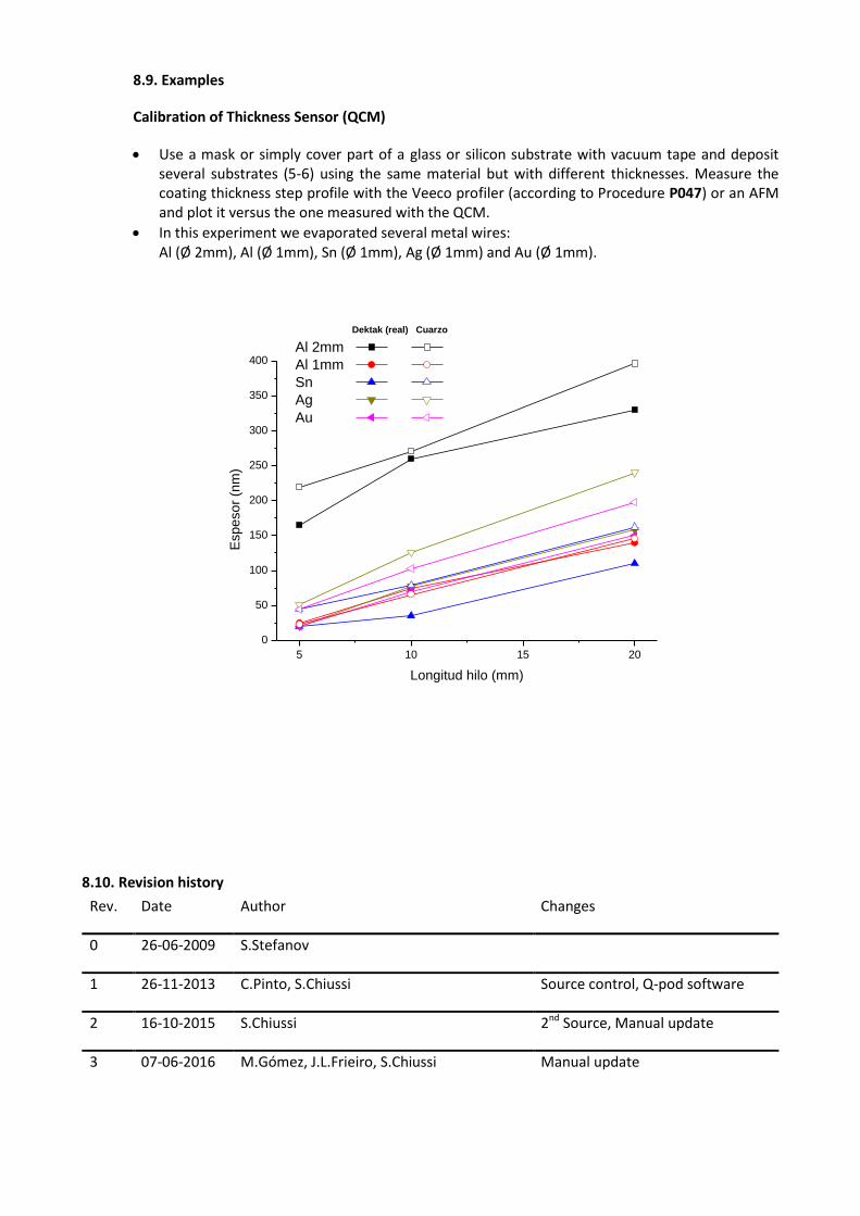
8.9. Examples
Calibration of Thickness Sensor (QCM)
Use a mask or simply cover part of a glass or silicon substrate with vacuum tape and deposit several substrates (5-6) using the same material but with different thicknesses. Measure the coating thickness step profile with the Veeco profiler (according to Procedure P047) or an AFM and plot it versus the one measured with the QCM.
In this experiment we evaporated several metal wires: Al (Ø 2mm), Al (Ø 1mm), Sn (Ø 1mm), Ag (Ø 1mm) and Au (Ø 1mm).
5 10 15 20
0
50
100
150
200
250
300
350
400
Esp
eso
r (n
m)
Longitud hilo (mm)
Al 2mm
Al 1mm
Sn
Ag
Au
Dektak (real) Cuarzo
8.10. Revision history
Rev. Date Author Changes
0 26-06-2009 S.Stefanov
1 26-11-2013 C.Pinto, S.Chiussi Source control, Q-pod software
2 16-10-2015 S.Chiussi 2nd Source, Manual update
3 07-06-2016 M.Gómez, J.L.Frieiro, S.Chiussi Manual update
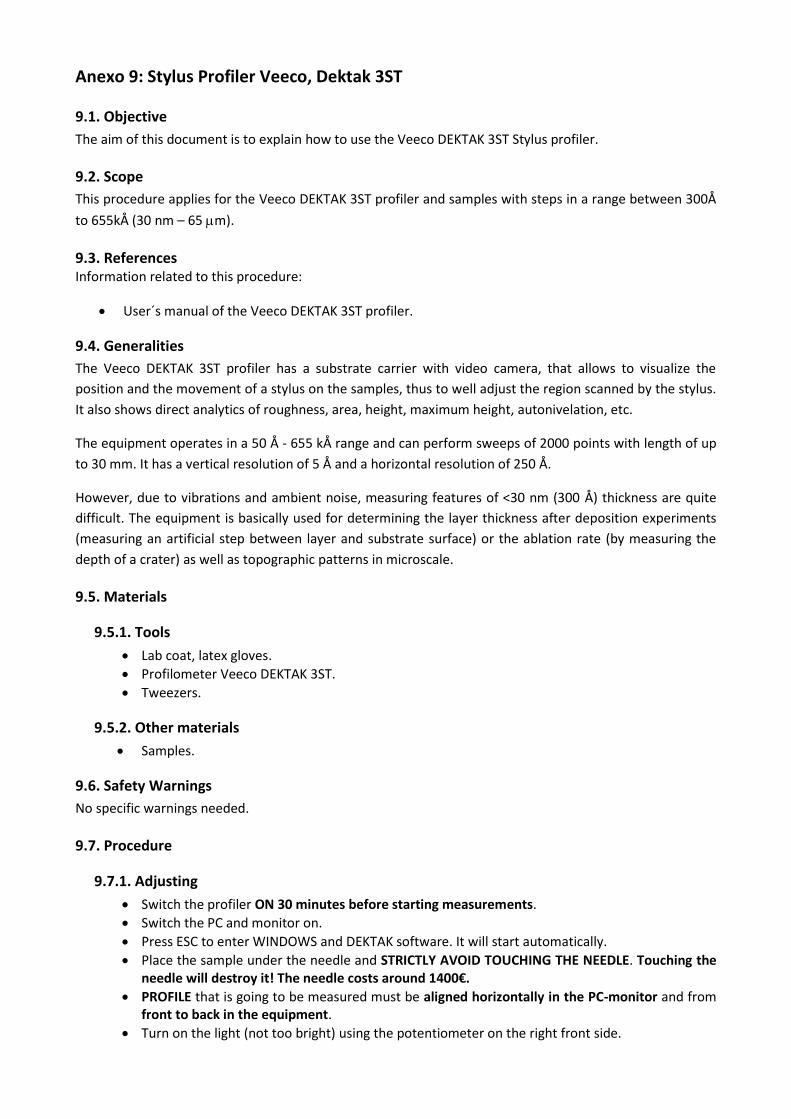
Anexo 9: Stylus Profiler Veeco, Dektak 3ST
9.1. Objective
The aim of this document is to explain how to use the Veeco DEKTAK 3ST Stylus profiler.
9.2. Scope
This procedure applies for the Veeco DEKTAK 3ST profiler and samples with steps in a range between 300Å
to 655kÅ (30 nm – 65 m).
9.3. References Information related to this procedure:
User´s manual of the Veeco DEKTAK 3ST profiler.
9.4. Generalities The Veeco DEKTAK 3ST profiler has a substrate carrier with video camera, that allows to visualize the
position and the movement of a stylus on the samples, thus to well adjust the region scanned by the stylus.
It also shows direct analytics of roughness, area, height, maximum height, autonivelation, etc.
The equipment operates in a 50 Å - 655 kÅ range and can perform sweeps of 2000 points with length of up
to 30 mm. It has a vertical resolution of 5 Å and a horizontal resolution of 250 Å.
However, due to vibrations and ambient noise, measuring features of <30 nm (300 Å) thickness are quite
difficult. The equipment is basically used for determining the layer thickness after deposition experiments
(measuring an artificial step between layer and substrate surface) or the ablation rate (by measuring the
depth of a crater) as well as topographic patterns in microscale.
9.5. Materials
9.5.1. Tools
Lab coat, latex gloves.
Profilometer Veeco DEKTAK 3ST.
Tweezers.
9.5.2. Other materials
Samples.
9.6. Safety Warnings
No specific warnings needed.
9.7. Procedure
9.7.1. Adjusting
Switch the profiler ON 30 minutes before starting measurements.
Switch the PC and monitor on.
Press ESC to enter WINDOWS and DEKTAK software. It will start automatically.
Place the sample under the needle and STRICTLY AVOID TOUCHING THE NEEDLE. Touching the needle will destroy it! The needle costs around 1400€.
PROFILE that is going to be measured must be aligned horizontally in the PC-monitor and from front to back in the equipment.
Turn on the light (not too bright) using the potentiometer on the right front side.
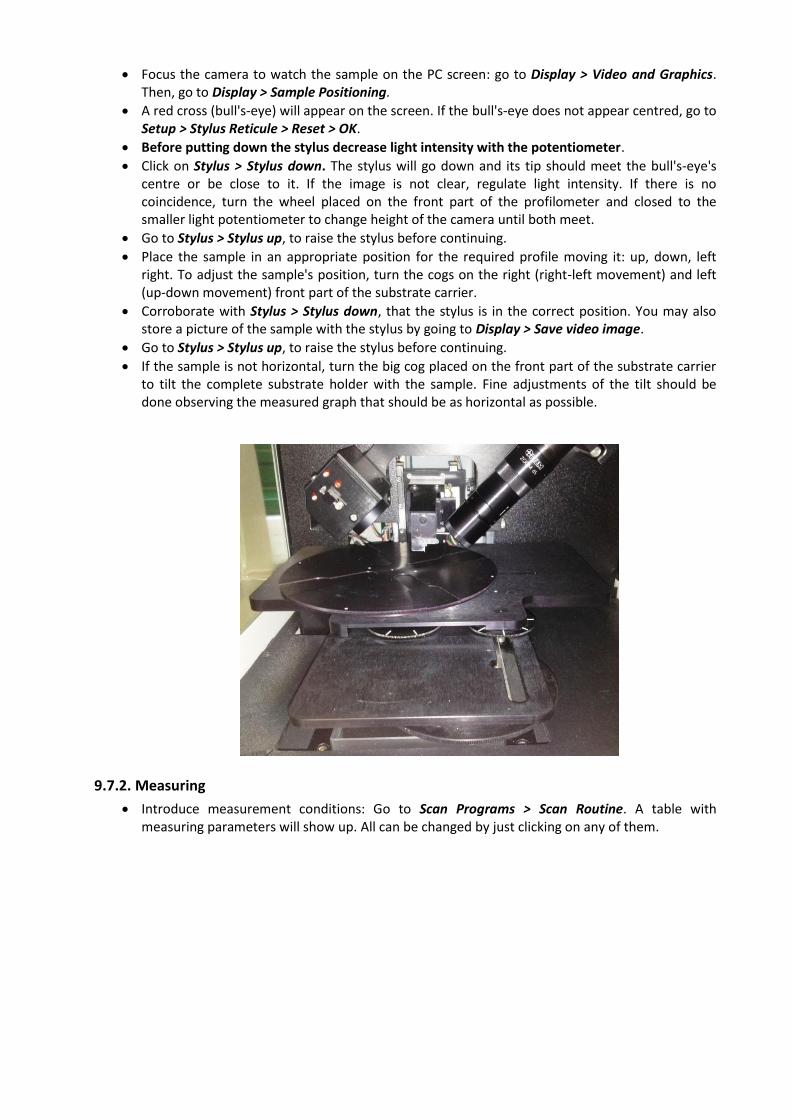
Focus the camera to watch the sample on the PC screen: go to Display > Video and Graphics. Then, go to Display > Sample Positioning.
A red cross (bull's-eye) will appear on the screen. If the bull's-eye does not appear centred, go to Setup > Stylus Reticule > Reset > OK.
Before putting down the stylus decrease light intensity with the potentiometer.
Click on Stylus > Stylus down. The stylus will go down and its tip should meet the bull's-eye's centre or be close to it. If the image is not clear, regulate light intensity. If there is no coincidence, turn the wheel placed on the front part of the profilometer and closed to the smaller light potentiometer to change height of the camera until both meet.
Go to Stylus > Stylus up, to raise the stylus before continuing.
Place the sample in an appropriate position for the required profile moving it: up, down, left right. To adjust the sample's position, turn the cogs on the right (right-left movement) and left (up-down movement) front part of the substrate carrier.
Corroborate with Stylus > Stylus down, that the stylus is in the correct position. You may also store a picture of the sample with the stylus by going to Display > Save video image.
Go to Stylus > Stylus up, to raise the stylus before continuing.
If the sample is not horizontal, turn the big cog placed on the front part of the substrate carrier to tilt the complete substrate holder with the sample. Fine adjustments of the tilt should be done observing the measured graph that should be as horizontal as possible.
9.7.2. Measuring
Introduce measurement conditions: Go to Scan Programs > Scan Routine. A table with measuring parameters will show up. All can be changed by just clicking on any of them.

Note: It is recommended to select the double step to avoid errors due to a horizontal tilt of the
sample.
Close the measuring compartment to avoid noise produced by air vibrations (movements or sounds). To start measuring click on Run > Run Single Scan. The stylus will go down and start moving. BE CAREFUL: DO NOT TOUCH THE TABLE TO AVOID VIBRATIONS. At the same time the measuring process is taking place, its corresponding graph will show up on the screen.
If the graph is not horizontal and close to zero it is necessary to adjust the horizontal tilt of the sample by moving the big cog. Repeat this process until the sample is leveled.
To obtain the right measurement of the layer's width and thickness, it is necessary to level the base line. Using the mouse, place the green (M) and red (R) lines close to the step and go to Plot > Level.
Save your data. Click on Data > Export Data > Options > Raw Scan Data.
Quit the program: Program Manager > File > Exit Windows. Switch off the computer, the potentiometer for the light, and finally the DEKTAK 3ST.
9.7.3. Data processing
Read the data (a txt file) with the software called ASCII changer that you can launch clicking the corresponding icon on the desktop by clicking File -> Open.
Click MAKE ASCII to convert the file in a files useful for Excel or Origin. The name will be tha same as the Original one but ASCII will be added to the name.
9.7.4. Additional way to save images
Click on the AAA Screen Capture icon (next to the clock) with the right button, go to Capture, double click rectangle area and define the area that you wish to copy.
For storing select the type of image you want to save (.bmp or .jpg) and decide a name.
You can change the background and turn it white selecting Image/negative using the IView 32 software (see corresponding desktop icon).
To print from IView 32, select Print.
There are two printing options: - Best fit: prints the graph in a big size.

- Scale: set x and y to 1 and select Refresh. It prints the graph in a reduced size.
9.8. Calculations and Uncertainties
Not considered.
9.9. Example
Not available.
9.10. Revision history
Rev. Date Author Changes
3 22-09-2000
4 -11-13 C.Pinto, S.Chiussi
5 22-02-2016 M.Gómez, J.L.Frieiro, S.Chiussi

Anexo 10: Particles in air measurements
10.1. Objective
The aim of this document is to show how to measure the concentration of particles in the FA3 Clean room atmosphere, to control filter contamination and Clean room Class.
10.2. Scope
This procedure applies to the equipment available in the Clean room of the FA3 group at the University of Vigo and has to be executed in the FA3 Clean room itself.
10.3. References
Documents related to this procedure:
Lighthouse Worldwide Solutions Handheld 3016 Operating Manual.
Software: LMS Express 7 (CD)
LMS Express 7 Operating Manual (CD)
10.4. Generalities
The cleanliness of a Clean Room is the parameter used for its classification, using ISO 14644-1. ISO classes range from 1 (cleanest) to 9 (dirtiest). Since most of the contamination in a Clean Room is contained in the air, controlling the particle's sizes and concentration per volume is fundamental. The smaller the particles and the lesser their concentration, the better is the ISO class of the Clean Room. Within the ISO, the maximum concentration of particles for considered sizes that are allowed at each class (particles/m3 of air), is stated as follows:
10.5. Materials
Lab coat, shoe covers, hair cover and latex gloves (as instructed in https://en.wikipedia.org/wiki/Cleanroom_suit).
Handheld 3016.
10.6. Safety Warnings
Do not operate: o with reactive gases (O2 or H2), o at a lower pressure than atmospheric, or o with a different density than that of ambient air as these may damage the instrument.
Avoid liquids of any kind from going into the instrument.
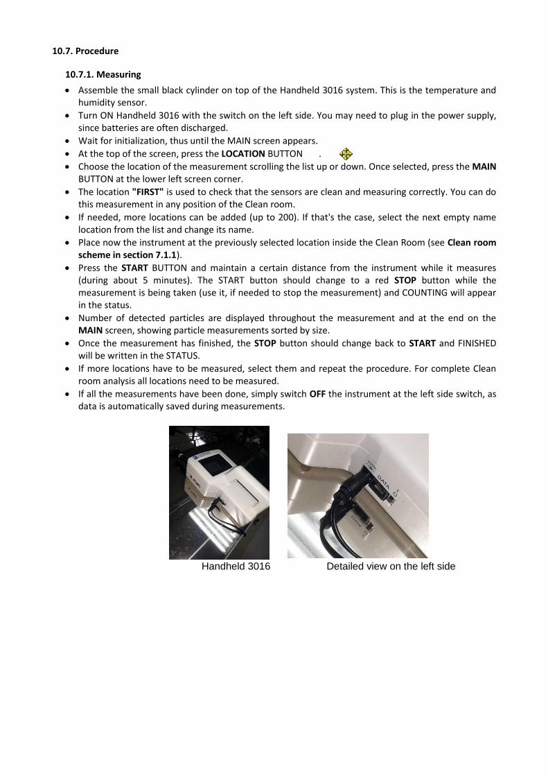
10.7. Procedure
10.7.1. Measuring
Assemble the small black cylinder on top of the Handheld 3016 system. This is the temperature and humidity sensor.
Turn ON Handheld 3016 with the switch on the left side. You may need to plug in the power supply, since batteries are often discharged.
Wait for initialization, thus until the MAIN screen appears.
At the top of the screen, press the LOCATION BUTTON .
Choose the location of the measurement scrolling the list up or down. Once selected, press the MAIN BUTTON at the lower left screen corner.
The location "FIRST" is used to check that the sensors are clean and measuring correctly. You can do this measurement in any position of the Clean room.
If needed, more locations can be added (up to 200). If that's the case, select the next empty name location from the list and change its name.
Place now the instrument at the previously selected location inside the Clean Room (see Clean room scheme in section 7.1.1).
Press the START BUTTON and maintain a certain distance from the instrument while it measures (during about 5 minutes). The START button should change to a red STOP button while the measurement is being taken (use it, if needed to stop the measurement) and COUNTING will appear in the status.
Number of detected particles are displayed throughout the measurement and at the end on the MAIN screen, showing particle measurements sorted by size.
Once the measurement has finished, the STOP button should change back to START and FINISHED will be written in the STATUS.
If more locations have to be measured, select them and repeat the procedure. For complete Clean room analysis all locations need to be measured.
If all the measurements have been done, simply switch OFF the instrument at the left side switch, as data is automatically saved during measurements.
Handheld 3016 Detailed view on the left side

Main screen
Location selection screen
10.7.1.1 Locations to measure
NAME IN HANDHELD 3016 CLEANROOM PLACE
FIRST First
EVAPOR Evaporator
ENTRADA Entrance
CABINA Cabin
INDI INDI laser
SISTEMA UHV system
CLIMATIZ Air conditioning system entrance
RAMAN Raman spectometers
DEKTAK DEKTAK Profiler
TRR TRR (Optical bench for TRR)
LAVABO Sink corner
PLD PLD system

10.7.2. Downloading data
ATTENTION: The specific USB key is needed to open the program. Open the LMS Express 7 program. Connect the instrument to the computer, click Home button and Data Collection. In Other Options, click Manual Data Download. Click Download Data button to start the Manual Data Download Wizard.
On the following screen click NEXT and then select the port used to connect the instrument on the Serial Port list and leave the address set to <Auto-Detect>. Click NEXT to continue. After the connection has been established click NEXT again to start downloading data. ATTENTION: While downloading data, Location Names of the instrument are ignored. Instead, Location Names of the instrument are matched with the program's short Location names and assigned location numbers. If downloaded data come from a location name that does not match a short location name in the program, a Synchronization Issue dialog window appears. If the user chooses to synchronize the location’s name, the location name of the instrument is overwritten (section 7.2.1.). After the data is downloaded, the program displays the following message:
Mob. Evaporator Mob. Aux. table
Gasses, etc.
ChairPerson
Ch
air
Pe
rson
Electric meas.
Eact
meas.
4 p
oin
ts
ChairPerson
Ch
air
Pe
rson
Ell
ipso
me
ter
Mob. RackLPX
INDI
UHV bench and systems
Aux. table
Ch
air
Pe
rso
n
Table withoptical
benches
PLD
COMPEX
Shelves
Doors+
Cabinets
Doors+
Cabinets
H-Effusion
Mo
p
Sin
k, a
ux.
ta
ble Sticky mat
AIR HEPAS
cre
en
FT-Raman
De
kta
k
Po
we
rsu
pp
ly
Aux. table
Mobile Raman+ PC
FLOW BOX AV 30/70
Spin Coater
Ultra
so
un
ds
Water, sink
PC
Ar
P-3
P-4
P-9
P-7
P-8
Particle measurement points:
P-1: First (random meas.)P-2: EvaporatorP-3: EntranceP-4: CabinP-5: INDI
P-6: UHV systemP-7: ClimatizationP-8: RamanP-9: DEKTAKP-10: TRR
S c r e e nK e y b o a r d
Nikon
An
g.
Co
un
t.
Sticky mat
Sticky mat
Purif.
AIR HEPA
Curtains
Purif.
Vaccumcleaner
N2
intakeN2
intake
AIR exit
P-11: Sink cornerP-12: PLD
P-2
H2Ne
Sticky mat
Stickym
at
P-11
P-12
P-10
P-5
P-6
Ladder
Sticky mat

Select NO to leave the data history in the equipment intact (the usual case). Click FINISH to leave the Manual Data Download Window.
7.2.1. Changing locations
ATTENTION: It's only necessary to change the locations the first time that data are downloaded, that
is, when new locations have been added or the order has been changed. For the next downloads the
data are added automatically.
In the Administrator Options view, click on "Location Numbers and Names”. A list with all the
locations will appear.
To change a name, select the location and double click it. The following window will appear:
In this window, changes to the Long Name (name used by the program) and the short name (name
used by the instrument) can be made.
10.8. Calculations and Uncertainties
Not specified.
10.9. Examples
For the date stated on the last revision (section 10), the ISO class for the FA3 Clean Room is Class 7 with
Class 6 and Class 2 zones.
10.10. Revision history
Rev. Date Author Changes
0 15-02-2016 M.Gómez, J.L.Frieiro, S.Chiussi
Anexo 11: Graphing particles in air measurements
11.1. Objective
The aim of this document is to explain how to create a graph with the data downloaded from the Handheld 3016 (according to the procedure P020-Particles in air measurements).
11.2. Scope
This procedure applies to the equipment available in the Clean Room of the FA3 group at the University of Vigo.
11.3. References
Documents related to this procedure:
Lighthouse Worldwide Solutions Handheld 3016 Operating Manual.
LMS Express 7 Operating Manual (CD)
11.4. Generalities
The cleanliness of a Clean Room is the parameter used for its classification, using ISO 14644-1. ISO classes range from 1 (cleanest) to 9 (dirtiest). Since most of the contamination in a Clean Room is contained in the air, controlling the particle's sizes and concentration per volume is fundamental. The smaller the particles and the lesser their concentration, the better ISO class of the Clean Room. Within the ISO, the maximum concentration of particles for considered sizes that are allowed at each class (particles/m3 of air), is stated as follows:
11.5. Materials
Software: LMS Express 7 (in the CD)
11.6. Safety Warnings
Not specified.
11.7. Procedure
Once the data has been downloaded (see P020-Particles in air measurements) they can be represented in
a graph to ease the reading of the measurements and follow up the evolution of the Clean room quality.
In order to do so, display the Graph view in the program by clicking the HOME button and then Graphs at
the Home menu.
On the left side, click on "Create a New Graph" and the Graph Setup
window will appear. Enter a name and setup, who owns the graph and who
can see it. Click on the Data tab and something similar to the following
image will appear:
Select the axis to represent the data. Select the data set(s) that are to be plotted, pressing the ADD button
for each one. After all the data has been selected, click OK.
Now, click the "Time Range" tab and select the type of graph desired and the time to be shown.
On the "Scale" tab you can change between a linear or logarithmic scale. Set up control lines if necessary at
the "Control Lines" tab.
When all the options have been set, click OK and the graph will be showed. At the Graph view, any graph
created before can be shown.
11.8. Calculations and Uncertainties
Not specified.
11.9. Examples
For the date of the last revision (section 10), the ISO class for the FA3 Clean Room is Class 7 with Class 6 and
Class 2 zones.
11.10. Revision history
Rev. Date Author Changes
0 17-02-2016 M.Gómez, J.L.Frieiro, S.Chiussi

Anexo 11: Figuras
Figura 1. Oblea de silicio cortada y marcada.

Figura 2. Muestras tras el depósito de Al, con las máscaras de electrodos todavía colocadas.
Figura 3. Muestra lista para ser medida con el perfilómetro Dektak 3ST.

Figura 4. Estructura típica de medidas TLM.