Embed Size (px)
Citation preview

AAllmmaa MMaatteerr SSttuuddiioorruumm –– UUnniivveerrssiittàà ddii BBoollooggnnaa
DOTTORATO DI RICERCA IN
SCIENZE CHIMICHE
Ciclo XXVI
Settore Concorsuale di afferenza: 03/C2 Settore Scientifico disciplinare: CHIM/05
TITOLO TESI
CHARGE TRANSPORT PROPERTIES OF ORGANIC CONJUGATED POLYMERS FOR PHOTOVOLTAIC
APPLICATIONS
Presentata da: Sara Righi Coordinatore Dottorato Relatore
Prof. Aldo Roda Prof. Stefano Stagni
Correlatori
Dr.ssa Nadia Camaioni
Dr.ssa Francesca Tinti
Esame finale anno 2014


To my family and to my friend and sister Roberta

I
ABSTRACT
Charge transport in conjugated polymers as well as in bulk-heterojunction
(BHJ) solar cells made of blends between conjugated polymers, as electron-donors
(D), and fullerenes, as electron-acceptors (A), has been investigated.
It is shown how charge carrier mobility of a series of anthracene-containing
poly(p-phenylene-ethynylene)-alt-poly(p-phenylene-vinylene)s (AnE-PVs) is highly
dependent on the lateral chain of the polymers, on a moderate variation of the
macromolecular parameters (molecular weight and polydispersity), and on the
processing conditions of the films. For the first time, the good ambipolar transport
properties of this relevant class of conjugated polymers have been demonstrated,
consistent with the high delocalization of both the frontier molecular orbitals.
Charge transport is one of the key parameters in the operation of BHJ solar
cells and depends both on charge carrier mobility in pristine materials and on the
nanoscale morphology of the D/A blend, as proved by the results here reported. A
straight correlation between hole mobility in pristine AnE-PVs and the fill factor of
the related solar cells has been found.
The great impact of charge transport for the performance of BHJ solar cells is
clearly demonstrated by the results obtained on BHJ solar cells made of neat-C70,
instead of the common soluble fullerene derivatives (PCBM or PC70BM). The
investigation of neat-C70 solar cells was motivated by the extremely low cost of
non-functionalized fullerenes, compared with that of their soluble derivatives
(about one-tenth). For these cells, an improper morphology of the blend leads to a
deterioration of charge carrier mobility, which, in turn, increases charge carrier
recombination. Thanks to the appropriate choice of the donor component, solar
cells made of neat-C70 exhibiting an efficiency of 4.22% have been realized, with an
efficiency loss of just 12% with respect to the counterpart made with costly
PC70BM.
II
TABLE OF CONTENTS
ABSTRACT I
1. INTRODUCTION 1
1.1 The promise of organic electronics 1
1.2 Organic conjugated materials 3
1.3 Charge transport in organic solids 5
1.4 Organic solar cells 7
1.5 Charge transport and loss channels in organic solar cells 9
1.6 Aim of the thesis 11
2. EXPERIMENTAL METHODS 13
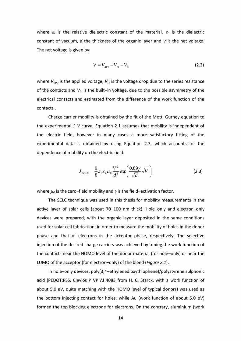
2.1 Measurement of charge carrier mobility 13
2.1.1 Space-charge limited-current 13
2.1.2 Time of Flight 15
2.1.3 Admittance spectroscopy 16
2.2 Solar cells: preparation and characterization 19
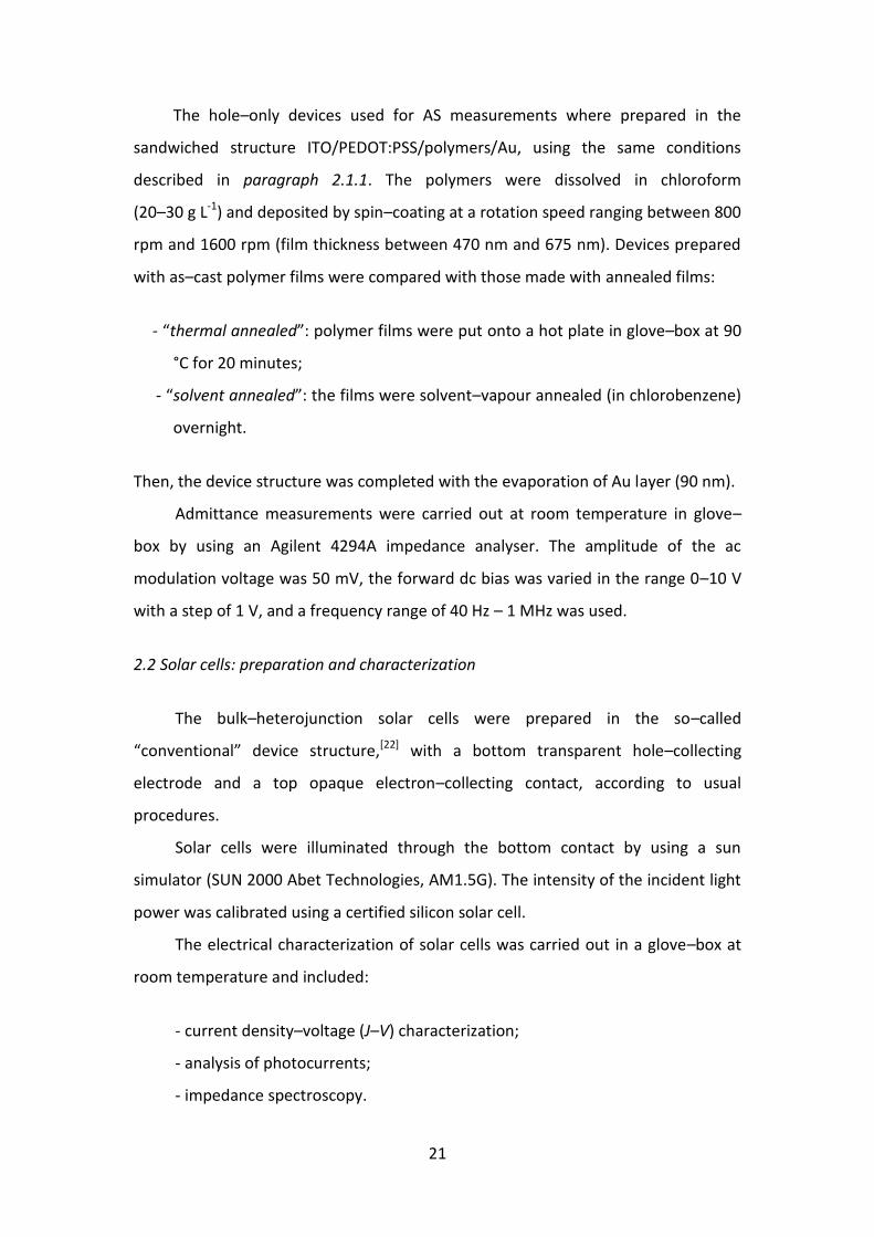
2.2.1 Device preparation 21
2.2.2 Current-voltage characterization 22
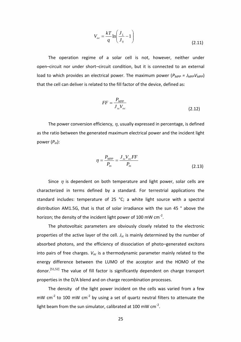
2.2.3 Analysis of photocurrents 26
2.2.4 Impedance spectroscopy 28
3. CHARGE TRANSPORT IN ANTHRACENE-CONTAINING
POLY((P-PHENYLENE-ETHYNYLENE) -ALT-POLY(P-PHENYLENE-
VINYLENE))S
30
3.1 Materials 31
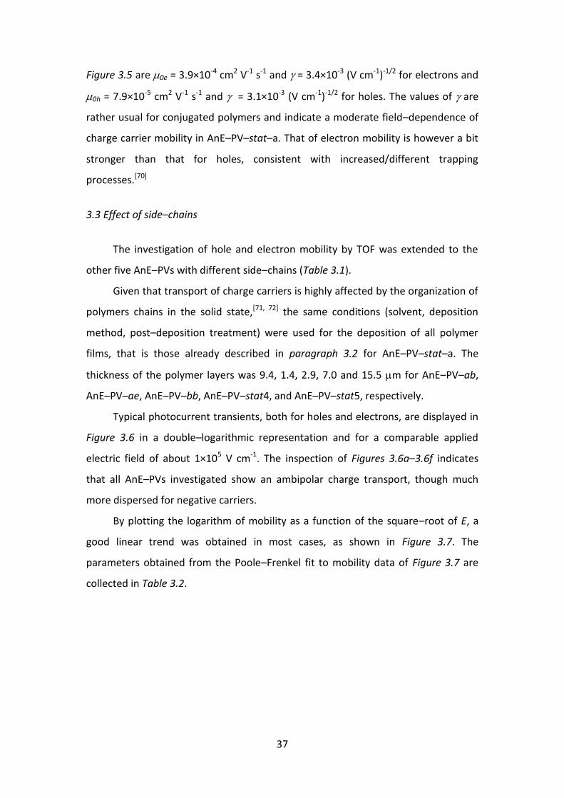
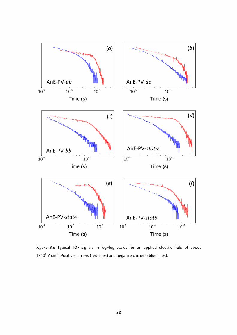
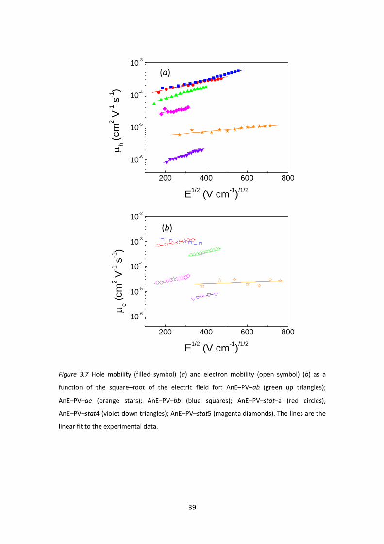
3.2 Ambipolar behaviour 33
3.3 Effect of side-chains 37
3.4 Effect of solvent and thermal treatments 44
3.5 Effect of a fine variation of the macromolecular parameters 49
3.5.1 Effect on the optical properties 50
III
3.5.2 Effect on the structural and morphological properties 52
3.5.3 Effect on charge carrier mobility 56
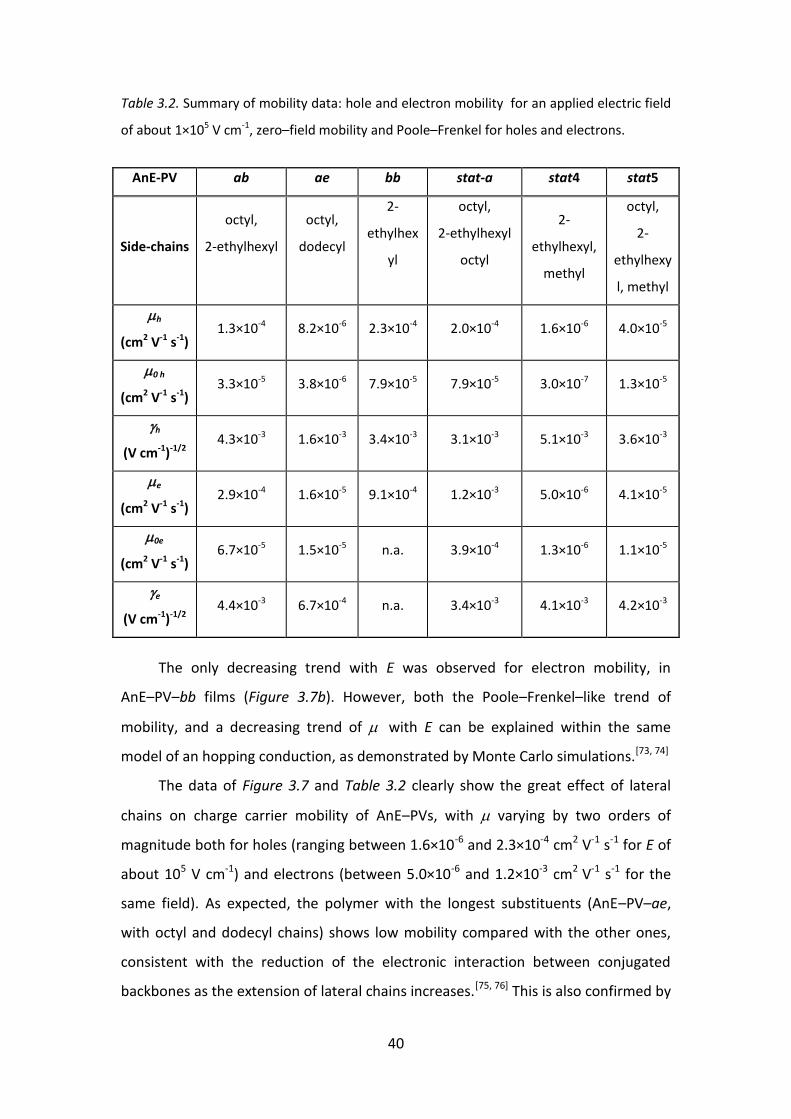
3.5.4 Effect on the performance of BHJ solar cells 58
3.6 Discussion 61
4. CHARGE TRANSPORT IN SOLAR CELLS MADE OF LOW BANDGAP
CONJUGATED POLYMERS AND NEAT-C70
64
4.1 Materials 64
4.2 Solar cells made of neat-C70 as electron acceptor 66
4.2.1 Photovoltaic parameters 66
4.2.2 Analysis of photocurrents 71
4.2.3 Charge carrier mobility 75
4.2.4 Impedance spectra 77
4.2.5 Blend morphology 79
4.3 The use of pyrene as C70 disperdant 82
4.3.1 Blend morphology 83
4.3.2 Photovoltaic parameters 84
4.3.3 Analysis of photocurrents 87
4.3.4 Charge carrier mobility 89
4.3.5 Impedance spectra 90
4.4 Discussion 93
5. CONCLUDING REMARKS 96
LIST OF PUBLICATIONS 98
REFERENCES
ACKNOWLEDGEMENTS
99
103
1
CHAPTER 1 – INTRODUCTION
1.1 The promise of organic electronics
Nowadays we live in an electronic world, indeed the use of personal
computers, tablets and smart phones is steadily increasing. In 2012, there were an
estimated 30–40 processors per person, on average, with some individuals
surrounded by as many as 1000 processors on a daily basis.[1] However, the
resources and methodologies used to fabricate electronic devices bring up urgent
questions about the negative environmental impacts of the manufacture, use, and
disposal of electronic devices.
The use of organic conjugated materials[2,3] to produce electronic devices could
enable a more eco–friendly and sustainable way to let the electronic world grow.
Chemists are synthesizing a wealth of new organic materials for use in electronic
devices, which enable novel properties impossible to be replicated with traditional
inorganic semiconductors like silicon. These carbon–based materials, like the ones of
living things, hold the promise to expand our electronic landscape in ways that will
radically change the way society interacts with technology. Indeed, an electronics
made of organic materials, organic electronics, may be printed on flexible substrates
at room temperature, making possible electronic newspapers and magazines, smart
windows, flexible photovoltaic sheets and luminescent wallpapers. In other words,
organic materials give to electronic devices unique properties such as mechanical
flexibility, lightweight, sensing, biocompatibility and low–temperature
processing,[4-6] impossible to be achieved with silicon.
Some applications of organic electronics have already been realized, like OLED
(organic light emitting diodes) smartphones and low–cost solar cells being installed
on rooftops in rural off–grid communities in South Sudan. Some others, like the
ultra–thin OLED TVs and foldable smartphones, are expected to be launched in the
near future. Further applications, like electronic skin which mimics human skin with
its tactile sensitivity, will take longer. Still others cannot be foreseen. The potential
future applications are many and varied, spanning across multiple fields: medicine
and biomedical research, energy and environment, communications and
2
entertainment, home and office furnishings, clothing and personal accessories, and
more.
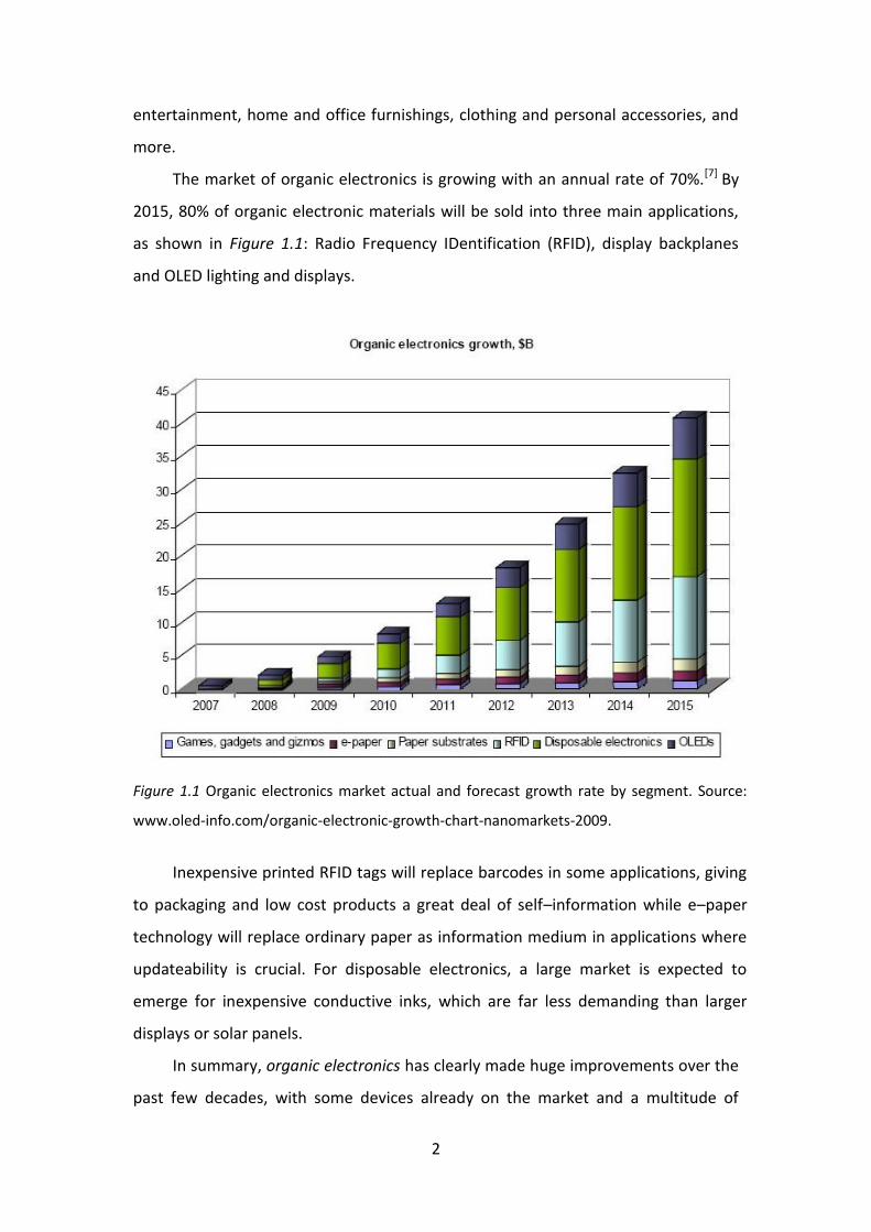
The market of organic electronics is growing with an annual rate of 70%.[7] By
2015, 80% of organic electronic materials will be sold into three main applications,
as shown in Figure 1.1: Radio Frequency IDentification (RFID), display backplanes
and OLED lighting and displays.
Figure 1.1 Organic electronics market actual and forecast growth rate by segment. Source:
www.oled-info.com/organic-electronic-growth-chart-nanomarkets-2009.
Inexpensive printed RFID tags will replace barcodes in some applications, giving
to packaging and low cost products a great deal of self–information while e–paper
technology will replace ordinary paper as information medium in applications where
updateability is crucial. For disposable electronics, a large market is expected to
emerge for inexpensive conductive inks, which are far less demanding than larger
displays or solar panels.
In summary, organic electronics has clearly made huge improvements over the
past few decades, with some devices already on the market and a multitude of
3
prototypes under development. It will continue to grow, changing the way society
interacts with technology. However, there are also challenges. Charge carrier
mobility of organic materials is typically orders of magnitude lower than its silicon
counterpart and its enhancement is expected to expand the market of organic
electronics.
1.2 Organic conjugated materials
Organic conjugated materials, small molecules and polymers,[8,9] have the
typical chemical structure with the alternation of single and double (or triple)
carbon–carbon bonds, determining their electronic properties. Single bonds are
referred as –bonds whereas double bonds embody one –bond and one –bond.
In a sigma bond the orbital overlapping is always along the inter–nuclear axis and
the probability to find the shared electron in a –bond is large between the two
carbon nuclei. The –bonds entail the electrons in the remaining p–orbital for each
carbon atom. The p–orbitals are electron clouds that are generally located above
and below each carbon atom. The overlapping of two atomic p–orbitals forms a
molecular –bond. The –bond does not overlap in the region directly between the
two carbon nuclei, where the –bond is combined, but it is found on the sides, for
example above and below, of the axis joining the two nuclei. In this case, the
probability to find the shared electron is larger a bit outside the direct line between
the two atoms, and at two places in the space surrounding the atoms.
Among organic conjugated materials, conjugated polymers are of particular
relevance for organic electronics. This because they combine electronic properties
similar to those of traditional semiconductors with the mechanical ones of common
plastics. Conjugated polymers have a –bond backbone of overlapping sp2–orbitals
and the remaining out–of–plane p–orbitals (pz) of the carbon atoms overlap with
neighbouring pz–orbitals to make the -bonding. The two overlapping positions are
called bonding () and anti bonding (*), the latter with a higher energy. The
–bonding electrons are free to move at certain distance over the molecular chain.
As an example, the molecular structure of ethylene, the simplest molecule with a

4
double carbon–carbon bond, is shown in Figure 1.2, together with the overlap of the
sp2–orbitals and the p–orbitals to form –bonds and –bonds.
Figure 1.2 Molecular structure of ethylene (above) and the overlap of atomic sp2 and
p–orbitals to form molecular and –bonds (below).
The features of the –bonds are the origin of the semiconducting properties of
organic conjugated materials. The semiconducting properties are enabled by the
quantum mechanical overlap of the p–orbitals that produces and * orbitals. The
highest energy orbital is called HOMO (Highest Occupied Molecular Orbital) and
the lowest energy * one is the LUMO (Lowest Unoccupied Molecular Orbital). The
difference in energy between these two levels is the energy gap, defining the
optoelectronic properties of organic conjugated materials.
The main advantages of organic conjugated materials, compared to inorganic
semiconductors, are:
- the availability of new organic materials is almost unlimited, while inorganic
semiconductors are still a few;
- the electronic properties of organic materials can be easily modulated through
molecular design;
- organic materials are lightweight;

5
- organic materials, if designed with appropriate side substituents, can be processed
from solution with printing techniques (ink-jet printing, screen printing, etc..) over
any substrate of large area;
- the absorption coefficient of organic materials is typically very high (> 105 cm-1).
The latter point is of particular interest for the photovoltaic application, for
which efficient absorption of sunlight in thin films is required.
1.3 Charge transport in organic solids
Charge transport properties constitute a major determining factor for the
operation of any electronic device and mainly for organic electronics, given the
much worse mobility of charge carriers in organic materials, compared to that in
conventional semiconductors. Indeed, the process of charge transport in organic
materials is very different from that of inorganic semiconductors, due to the
molecular nature of organic solids. While inorganic semiconductors show an energy
band structure and charge transport is a band–like process, in organic materials
charges are localized to single molecules and are not highly delocalized. Therefore,
charge transport in such localized systems occurs via an “hopping” process,[10] with
charge carriers tunnelling from one localized state to another within the lattice of
molecular sites. This localization as well as potential for collisions, scattering and
delays, result in charge carrier mobility typically ranging between 10-7 cm2 V-1 s-1 to
10 cm2 V-1 s-1 in organic solids,[11] orders of magnitude lower compared to inorganic
crystalline semiconductors.
In disordered organic materials hopping transport is a process determined by
two main factors:[12] the transfer integral and the reorganization energy. The
transfer integral represents basically the overlap of the HOMO levels, for hole
transport, and of the LUMO levels for electron transport. The magnitude of the
transfer integral is controlled by the wave functions of the –clouds, by their
orientations with respect to one another, and by their separation. The higher the
transfer integral is, the faster the hopping rate is, and the higher charge carrier
mobility is. The reorganization energy is the energy cost due to geometry
modifications to go from a neutral to a charged state and vice versa. The lower the
6
reorganization energy is, the smaller the geometry relaxations and the higher the
charge transfer rate are.
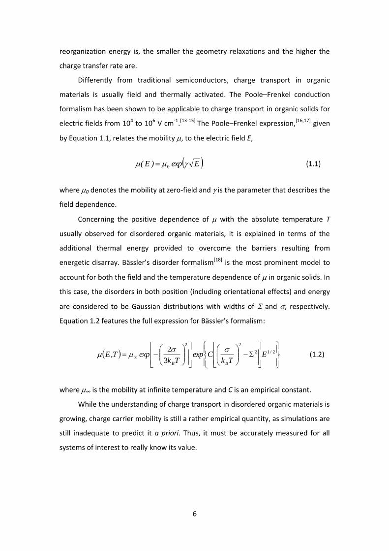
Differently from traditional semiconductors, charge transport in organic
materials is usually field and thermally activated. The Poole–Frenkel conduction
formalism has been shown to be applicable to charge transport in organic solids for
electric fields from 104 to 106 V cm-1.[13-15] The Poole–Frenkel expression,[16,17] given
by Equation 1.1, relates the mobility , to the electric field E,
Eexp)E( 0 (1.1)
where 0 denotes the mobility at zero-field and is the parameter that describes the
field dependence.
Concerning the positive dependence of with the absolute temperature T
usually observed for disordered organic materials, it is explained in terms of the
additional thermal energy provided to overcome the barriers resulting from
energetic disarray. Bässler’s disorder formalism[18] is the most prominent model to
account for both the field and the temperature dependence of in organic solids. In
this case, the disorders in both position (including orientational effects) and energy
are considered to be Gaussian distributions with widths of and , respectively.
Equation 1.2 features the full expression for Bässler’s formalism:
212
22
3
2 /
BB
ETk
CexpTk
expT,E
(1.2)
where ∞ is the mobility at infinite temperature and C is an empirical constant.
While the understanding of charge transport in disordered organic materials is
growing, charge carrier mobility is still a rather empirical quantity, as simulations are
still inadequate to predict it a priori. Thus, it must be accurately measured for all
systems of interest to really know its value.
7
1.4 Organic solar cells
The core of organic solar cells is the photoactive layer, which is generally
composed by two organic –conjugated materials with suitable energy levels: an
electron–donor (D) and an electron–acceptor (A).[19,20] Conjugated polymers or small
molecules are commonly used as electron–donors while soluble derivatives of
fullerene are commonly used as electron–acceptors. Fullerenes have not been
replaced yet by other acceptors because of their unique properties such as high
electron affinity and high electron mobility, making them the best
electron–acceptors till now.[21] The photoactive layer, typically around 100–200 nm
in thickness, is interposed between two collecting electrodes: the anode for positive
charge carriers and the cathode for electrons. Additional layers of electron or hole
transporting materials, are usually included at the interface between the active layer
and the electrodes for a more efficient collection of charge carriers.[22]
One of the main differences between inorganic semiconductors and organic
materials is given by the value of the relative dielectric constant, very low in organic
materials (~ 3), highly affecting the behaviour of the related solar cells. Indeed,
differently from inorganic semiconductors, the absorption of light with energy
higher than the energy gap does not lead to the generation of free pairs of charge
carriers in organic materials, but to Frenkel–type excitons. An exciton can be
considered as a bound state of an electron and a hole which are attracted each
other by the electrostatic Coulomb interaction. To allow exciton dissociation, a
driving force exceeding their binding energy (typically of 0.3–0.5 eV) is required. This
is possible at the D/A interface of the active layer of organic solar cells if the energy
offsets between the LUMO and HOMO levels of the two materials are sufficiently
high. In summary, the process leading to the generation of free charge carriers in
organic solar cells is much more complex than in the inorganic counterpart and is
composed of three steps:[23]
1. the photoexcitation of the absorber material(s) causes the promotion of electrons
from the ground state to the excited state, leading to the generation of
Frenkel–type excitons;
8
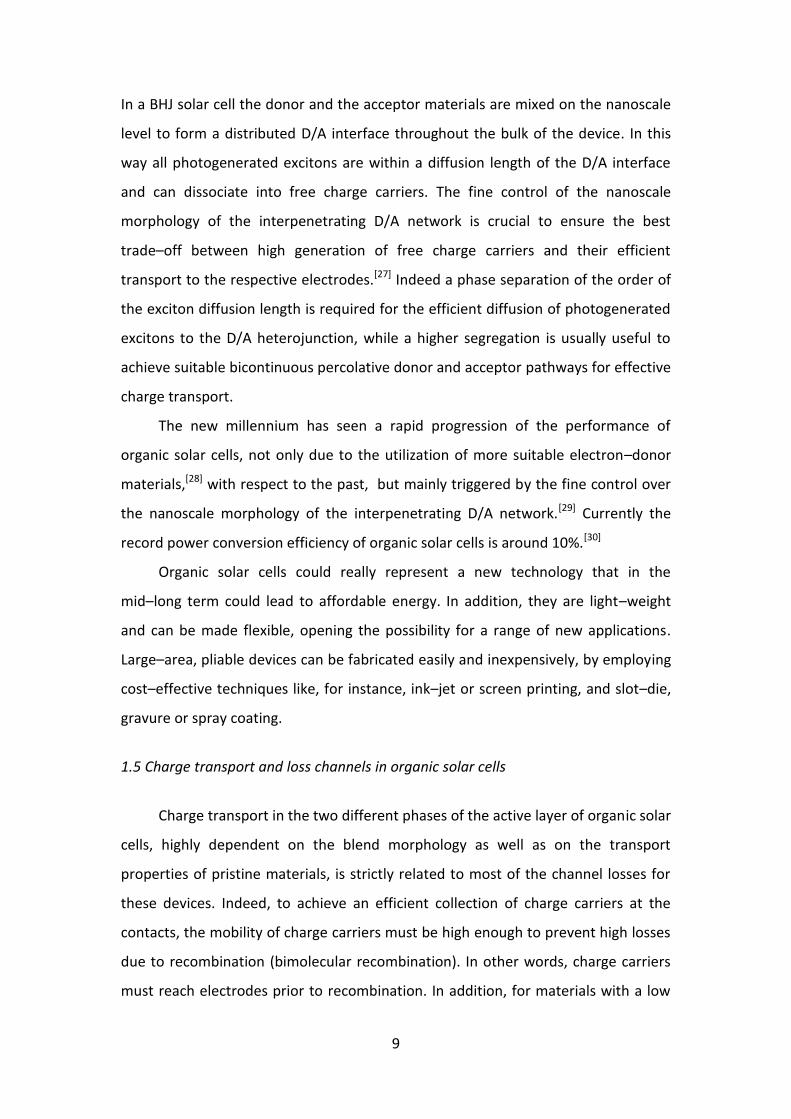
2. excitons photogenerated within a diffusion length (tipically 10–20 nm) from the
D/A interface have the chance to reach it before decaying, radiatively or not;
3. if the offsets of the energy levels of the D/A pair are higher than the exciton
binding energy, excitons can dissociate at the D/A interface. Excitons
photogenerated in the donor side dissociate by transferring the electron to the
LUMO level of the acceptor (photoinduced electron–transfer, Figure 1.3a) and
retaining the positive charge. Those created in the other side transfer the hole to
the HOMO of the donor (photoinduced hole–transfer) while retaining the
negative charge.
The role of an intermediate state between photogenerated excitons and
completely unbound electron–hole pairs, denoted as charge transfer state, is still
debated.[24] It could be responsible for the decay of the photoexcitation by
recombination of the bound electron–hole pair and leading to a loss for solar cells.
Free charge carriers originated from the dissociation of excitons are free to
move. They are transported through the respective materials (electrons in the
acceptor and holes in the donor) and collected at the respective electrodes.
The best approach for the active layer of organic solar cells is represented by
the intimate mixing of the donor and the acceptor material, the so–called
bulk–heterojunction (BHJ) approach (Figure 1.3b).[25,26]
+
Donor
-
Acceptor
(a) (b)
HOMO
HOMO
LUMO
LUMO
Figure 1.3 Photoinduced electron–transfer from the donor to the acceptor (a) and the
structure of a bulk–heterojuncion solar cell (b).
9
In a BHJ solar cell the donor and the acceptor materials are mixed on the nanoscale
level to form a distributed D/A interface throughout the bulk of the device. In this
way all photogenerated excitons are within a diffusion length of the D/A interface
and can dissociate into free charge carriers. The fine control of the nanoscale
morphology of the interpenetrating D/A network is crucial to ensure the best
trade–off between high generation of free charge carriers and their efficient
transport to the respective electrodes.[27] Indeed a phase separation of the order of
the exciton diffusion length is required for the efficient diffusion of photogenerated
excitons to the D/A heterojunction, while a higher segregation is usually useful to
achieve suitable bicontinuous percolative donor and acceptor pathways for effective
charge transport.
The new millennium has seen a rapid progression of the performance of
organic solar cells, not only due to the utilization of more suitable electron–donor
materials,[28] with respect to the past, but mainly triggered by the fine control over
the nanoscale morphology of the interpenetrating D/A network.[29] Currently the
record power conversion efficiency of organic solar cells is around 10%.[30]
Organic solar cells could really represent a new technology that in the
mid–long term could lead to affordable energy. In addition, they are light–weight
and can be made flexible, opening the possibility for a range of new applications.
Large–area, pliable devices can be fabricated easily and inexpensively, by employing
cost–effective techniques like, for instance, ink–jet or screen printing, and slot–die,
gravure or spray coating.
1.5 Charge transport and loss channels in organic solar cells
Charge transport in the two different phases of the active layer of organic solar
cells, highly dependent on the blend morphology as well as on the transport
properties of pristine materials, is strictly related to most of the channel losses for
these devices. Indeed, to achieve an efficient collection of charge carriers at the
contacts, the mobility of charge carriers must be high enough to prevent high losses
due to recombination (bimolecular recombination). In other words, charge carriers
must reach electrodes prior to recombination. In addition, for materials with a low

10
mobility, this puts also a restraint on the maximum thickness of the active layer,[31]
because a longer residence time of charge carriers in the film creates more chances
for recombination.
Bimolecular or non–geminate recombination is due to the recombination at
the D/A interface of free charge carriers of opposite sign coming from distinct
photoexcitation events (Figure 1.4a). Bimolecular recombination is mainly
determined by the mobility of the slowest charge carriers,[32] usually holes in the
donor phase.
Another type of recombination can occur in organic solar cells. After
photoinduced charge transfer, the still bound pairs of charges (charge transfer
states) that cannot escape the mutual Coulombic attraction will recombine at the
D/A interface (Figure 1.4b). In this case (monomolecular or geminate
recombination), charge carriers within a single photoexcitation event recombine, or
better, recombination occurs before complete dissociation of bound states at the
interface. Charge carrier mobility seems to play a relevant role also for geminate
recombination.[33]
Donor Acceptor
+
-
(b) Geminate recombination
Donor Acceptor
+
-
(a) Bimolecular recombination
LUMO
HOMO
LUMO
HOMO
LUMO
HOMO
CT
LUMO
HOMO
Figure 1.4 Bimolecular recombination of free charge carriers (a) and geminate
recombination of charge transfer (CT) states (b).
High charge carrier mobilities in the donor and in the acceptor phases are
required to reduce recombination losses in organic solar cells, but also balanced.
11
Indeed, strongly unbalanced mobilities, differing by more than one order of
magnitude, lead to the formation of space charge in the cell, due to the longer
residence time of the slowest carriers. Space charge formation strongly enhances
bimolecular recombination.[34]
In summary, charge transport in the bi–continuous D/A network is critical for
cell behaviour. Electron–donor materials showing high hole mobility are required for
the photovoltaic application, possibly comparable with that of common fullerene
derivatives (of the order of 10-3 cm2 V-1 s-1).[35] In addition to the good intrinsic
transport properties of the composing materials, the blend morphology has to
provide continuous pathways for the efficient transport of both type of charge
carriers to the respective electrodes.
1.6 Aim of the thesis
The aim of the work of the thesis is the investigation of charge transport, both
in pristine polymer films and in the active layer of bulk–heterojunction solar cells
made of conjugated polymers as electron–donors and fullerene as acceptor.
Charge carrier mobility in a series of anthracene–containing poly((p–
phenylene–ethynylene)–alt–poly(p–phenylene–vinylene))s (AnE-PVs) was studied as
a function of the electric field to understand the complex interplay between the
typical factors affecting charge transport properties (chemical structure,
macromolecular parameters and film processing conditions) and charge carrier
mobility in this relevant class of conjugated polymers. The strong correlation
between charge carrier mobility of pristine AnE–PV donors and the fill factor of
related bulk–heterojunction solar cells, was also demonstrated.
The investigation of the critical role of charge transport in the D/A double
network for the performance of organic photovoltaic devices was extended to
bulk–heterojunction solar cells made of two low–energy–gap conjugated polymers
and neat–C70 as acceptor. The replacing of common fullerene derivatives with neat–
fullerenes has a great advantage for an innovative photovoltaic technology as
organic photovoltaics, for which low–cost is one of the key factors. Indeed, the cost
of neat–fullerenes is roughly one tenth of that of common C60 or C70 derivatives,

12
chemically functionalised with suitable groups to enable an excellent
solubility/processability in chlorinated solvents.
Given the extremely poor solubility of pristine fullerenes,[36] very different
morphologies for the related D/A blends are expected, compared to those made of
functionalised C60/C70 derivatives, highly affecting both the dissociation of
photogenerated excitons and the transport of charge carriers. The aim of the work
is to find the conditions for the preparation of low–cost and high–efficiency organic
solar cells made of neat–fullerene.
13
CHAPTER 2 – EXPERIMENTAL METHODS
2.1 Measurement of charge carrier mobility
Common techniques for the measurement of mobility in traditional
semiconductors are not applicable to organic solids. This because undoped
conjugated materials are required for most organic electronic applications, including
the photovoltaic one, thus materials with a very low electrical conductivity, other
than with a relatively low charge carrier mobility. Hence, alternative techniques are
utilized for the characterization of charge transport in organic films, most of them
used in this thesis, such as, space–charge limited–current (SCLC),[37] time of flight
(TOF),[38] carrier extraction by linearly increasing voltage (CELIV),[39] and admittance
spectroscopy (AS).[40] TOF and AS methods were used in this thesis for the
investigation of charge carrier mobility in pristine polymer films, while the SCLC
technique was employed for the measurement of charge carrier mobility in the
donor and the acceptor phase of solar cells, this latter method being the most
best–suited for very thin films, like the active layer of organic photovoltaic devices.
2.1.1 Space–charge limited–current
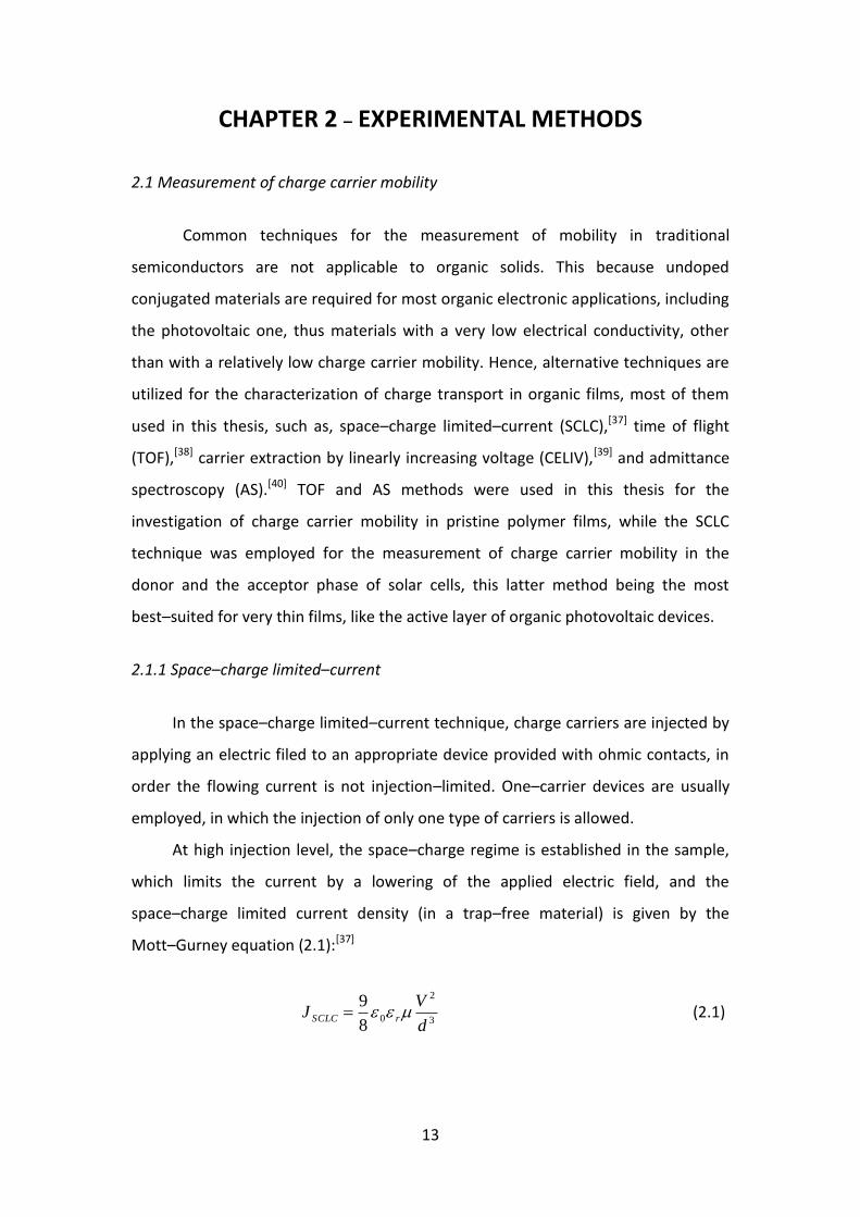
In the space–charge limited–current technique, charge carriers are injected by
applying an electric filed to an appropriate device provided with ohmic contacts, in
order the flowing current is not injection–limited. One–carrier devices are usually
employed, in which the injection of only one type of carriers is allowed.
At high injection level, the space–charge regime is established in the sample,
which limits the current by a lowering of the applied electric field, and the
space–charge limited current density (in a trap–free material) is given by the
Mott–Gurney equation (2.1):[37]
3
2
08
9
d
VJ rSCLC (2.1)
14
where r is the relative dielectric constant of the material, 0 is the dielectric
constant of vacuum, d the thickness of the organic layer and V is the net voltage.
The net voltage is given by:
birsapp VVVV (2.2)
where Vapp is the applied voltage, Vrs is the voltage drop due to the series resistance
of the contacts and Vbi is the built–in voltage, due to the possible asymmetry of the
electrical contacts and estimated from the difference of the work function of the
contacts .
Charge carrier mobility is obtained by the fit of the Mott–Gurney equation to
the experimental J–V curve. Equation 2.1 assumes that mobility is independent of
the electric field, however in many cases a more satisfactory fitting of the
experimental data is obtained by using Equation 2.3, which accounts for the
dependence of mobility on the electric field:
V
d
.exp
d
VJ rSCLC
890
8
93
2
00 (2.3)
where 0 is the zero–field mobility and is the field–activation factor.
The SCLC technique was used in this thesis for mobility measurements in the
active layer of solar cells (about 70–100 nm thick). Hole–only and electron–only
devices were prepared, with the organic layer deposited in the same conditions
used for solar cell fabrication, in order to measure the mobility of holes in the donor
phase and that of electrons in the acceptor phase, respectively. The selective
injection of the desired charge carriers was achieved by tuning the work function of
the contacts near the HOMO level of the donor material (for hole–only) or near the
LUMO of the acceptor (for electron–only) of the blend (Figure 2.1).
In hole–only devices, poly(3,4–ethylenedioxythiophene)/polystyrene sulphonic
acid (PEDOT:PSS, Clevios P VP AI 4083 from H. C. Starck, with a work function of
about 5.0 eV, quite matching with the HOMO level of typical donors) was used as
the bottom injecting contact for holes, while Au (work function of about 5.0 eV)
formed the top blocking electrode for electrons. On the contrary, aluminium (work

15
function of about 4.2 eV) was used in electron–only devices as the bottom blocking
contact for holes, while the electron injection contact was realized with LiF/Al (work
function of about 3.8 eV,[41] matching with the LUMO level of fullerenes).
Figure 2.1 Ideal energy scheme of hole–only (a) and electron–only (b) devices. The contacts
are represented with the Fermi energy level.
Hole–only devices were prepared onto glass substrates coated with
Indium–Tin–Oxide (ITO, Kintec, sheet resistance = 20 /, transmittance in the
visible range ~ 86% and work function ~ 4.8–4.9 eV), while electron–only ones on
glass. A selective chemical etching was used to pattern ITO electrodes. The
substrates were previously cleaned in detergent and water, and then ultrasonicated
in acetone and isopropyl alcohol for 15 minutes each.
PEDOT:PSS was spin–coated at 4000 rpm (~ 40 nm) onto UV–ozone–treated
ITO substrates, and then baked in an oven, in air, at 140°C for 10 minutes. Metal
layers were deposited by thermal evaporation at a base pressure of 3×10⁻⁶ mbar.
The blends were prepared and deposited as for solar cell fabrication
(described in paragraph 2.2.1 and in Chapter 3) onto ITO/PEDOT:SS or glass/Al, for
hole–only and electron–only devices, respectively. After the blend deposition, the
samples were transferred to an argon glove–box where the device structure was
completed with the evaporation of the top electrode. Au (70 nm) was used as the
top contact for hole–only devices and LiF/Al (20–80 nm) for electron–only ones. The
device active area, defined by the shadow mask used for the top electrode
deposition, was 25 mm2. The thickness of the blends, roughly the same of the active
layer of solar cells, was measured with a Tencor Alphastep 200 profilometer.
(a) LUMO
HOMO HOMO
LUMO(b)
contact
contactcontact
contact
16
The resulting device structure for hole–only and electron–only devices was
ITO/PEDOT:PSS/blend/Au and glass/Al/blend/LiF/Al, respectively. The electrical
characterization of the devices was carried out in glove–box at room temperature,
by using a Keithley 2400 source–measure unit to take the current–voltage curves.
2.1.2 Time of Flight
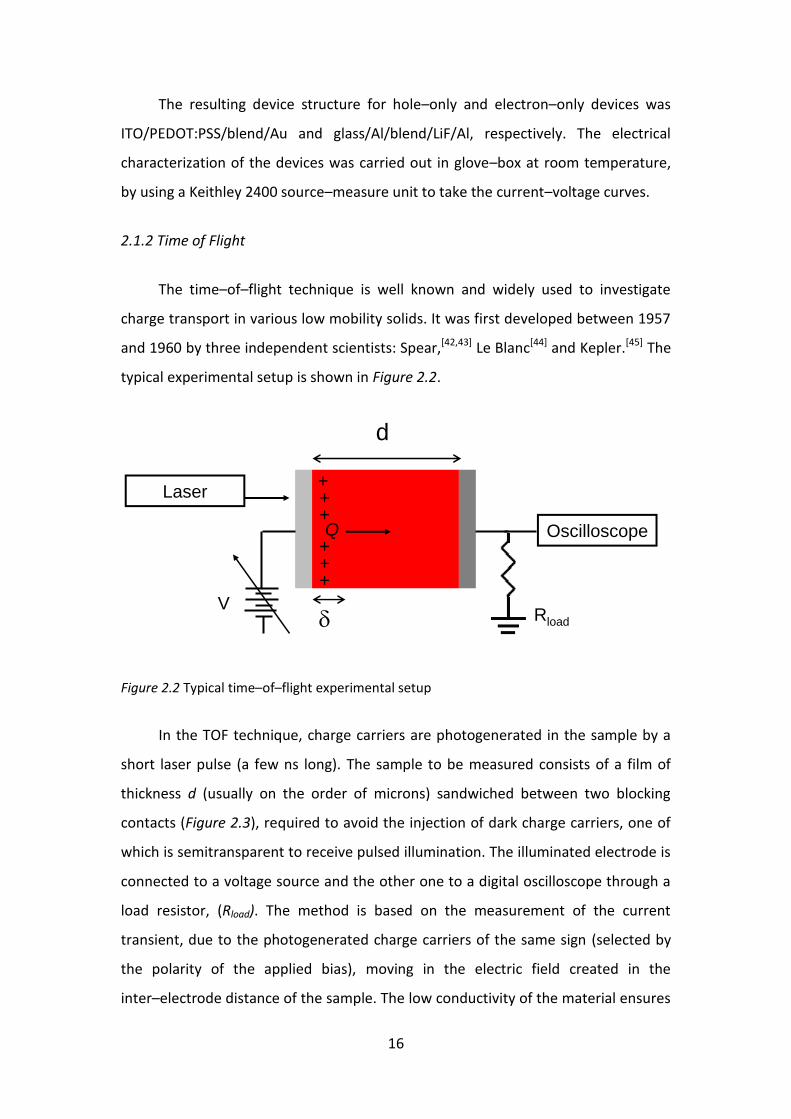
The time–of–flight technique is well known and widely used to investigate
charge transport in various low mobility solids. It was first developed between 1957
and 1960 by three independent scientists: Spear,[42,43] Le Blanc[44] and Kepler.[45] The
typical experimental setup is shown in Figure 2.2.
Figure 2.2 Typical time–of–flight experimental setup
In the TOF technique, charge carriers are photogenerated in the sample by a
short laser pulse (a few ns long). The sample to be measured consists of a film of
thickness d (usually on the order of microns) sandwiched between two blocking
contacts (Figure 2.3), required to avoid the injection of dark charge carriers, one of
which is semitransparent to receive pulsed illumination. The illuminated electrode is
connected to a voltage source and the other one to a digital oscilloscope through a
load resistor, (Rload). The method is based on the measurement of the current
transient, due to the photogenerated charge carriers of the same sign (selected by
the polarity of the applied bias), moving in the electric field created in the
inter–electrode distance of the sample. The low conductivity of the material ensures
d
V
Laser
Oscilloscope
Rload
Q
+++
+++
17
that, during the drift of the photogenerated charge carriers through the
inter–electrode distance, the density of equilibrium charge carriers will be too low to
redistribute the electric field inside the sample.
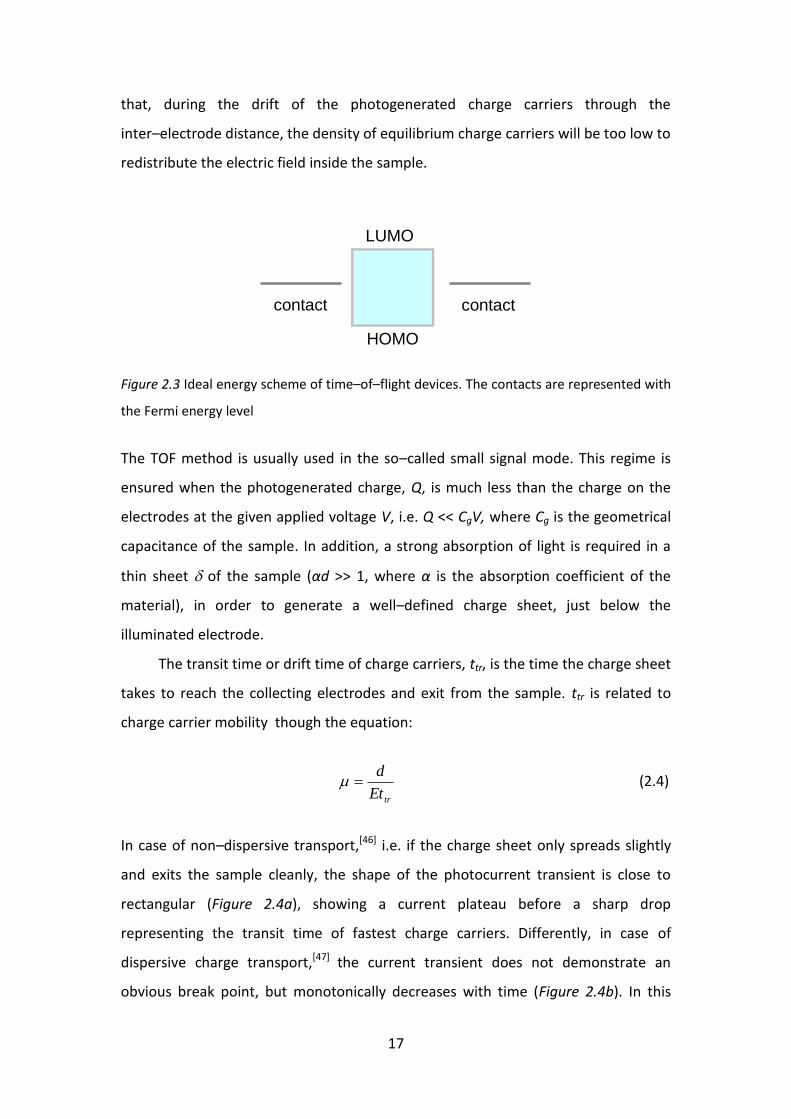
LUMO
HOMO
contactcontact
Figure 2.3 Ideal energy scheme of time–of–flight devices. The contacts are represented with
the Fermi energy level
The TOF method is usually used in the so–called small signal mode. This regime is
ensured when the photogenerated charge, Q, is much less than the charge on the
electrodes at the given applied voltage V, i.e. Q << CgV, where Cg is the geometrical
capacitance of the sample. In addition, a strong absorption of light is required in a
thin sheet of the sample (αd >> 1, where α is the absorption coefficient of the
material), in order to generate a well–defined charge sheet, just below the
illuminated electrode.
The transit time or drift time of charge carriers, ttr, is the time the charge sheet
takes to reach the collecting electrodes and exit from the sample. ttr is related to
charge carrier mobility though the equation:
trEt
d (2.4)
In case of non–dispersive transport,[46] i.e. if the charge sheet only spreads slightly
and exits the sample cleanly, the shape of the photocurrent transient is close to
rectangular (Figure 2.4a), showing a current plateau before a sharp drop
representing the transit time of fastest charge carriers. Differently, in case of
dispersive charge transport,[47] the current transient does not demonstrate an
obvious break point, but monotonically decreases with time (Figure 2.4b). In this

18
case, ttr is estimated by the inflection point of the current transient usually observed
when represented in a double–logarithmic scale.
Figure 2.4 Typical time–of–flight transients for non–dispersive charge transport (a), and
dispersive transport (b). The inset of (b) shows the signal in log–log scales.
The devices for TOF experiments were realized onto patterned glass/ITO or
Al–coated substrates. Polymer films were deposited by drop–casting from
1,2–dichlorobenzene or chlorobenzene solutions (30 g L-1), stirred for 4 days at
45–50 °C. After deposition, the films were solvent–vapour annealed in
chlorobenzene overnight. The device structure was completed with a vacuum
evaporated semitransparent aluminium layer (18 nm), acting as the illuminated
electrode. A nitrogen laser ( = 337 nm) with a pulse duration of 6–7 ns was used in
single–pulse mode to photogenerate charge carriers. A variable dc potential was
applied to the samples and, in order to ensure a uniform electric field inside the
device, the total photogenerated charge was kept less than 0.1 CgV. The
photocurrent was monitored across a variable load resistance by using a Tektronix
TDS620A digital oscilloscope. The TOF experiments were performed at room
temperature, under dynamic vacuum (8×10⁻⁶ mbar).
ttr
ttr
(a) (b)
19
2.1.3 Admittance spectroscopy
Admittance spectroscopy is a powerful tool for the investigation of
charge–carrier transport in high resistivity materials.[40] For the application of this
technique to the measurement of charge carrier mobility, charge carriers must be
injected into the sample, as for the SCLC method. Depending on the sign of the
carriers to be investigated, hole–only or electron–only devices are usually prepared.
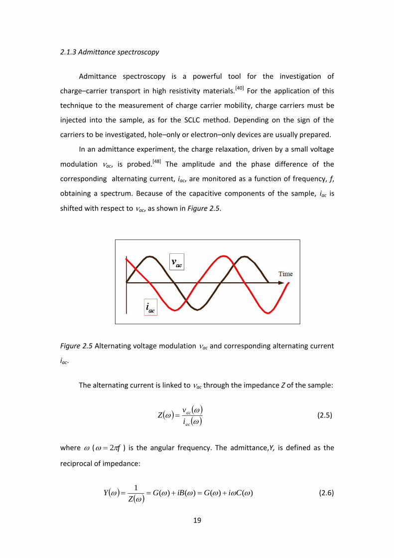
In an admittance experiment, the charge relaxation, driven by a small voltage
modulation ac, is probed.[48] The amplitude and the phase difference of the
corresponding alternating current, iac, are monitored as a function of frequency, f,
obtaining a spectrum. Because of the capacitive components of the sample, iac is
shifted with respect to ac, as shown in Figure 2.5.
Figure 2.5 Alternating voltage modulation ac and corresponding alternating current
iac.
The alternating current is linked to ac through the impedance Z of the sample:
ac
ac
i
vZ (2.5)
where ( f 2 ) is the angular frequency. The admittance,Y, is defined as the
reciprocal of impedance:
)()()()(1
CiGiBGZ
Y (2.6)

20
where its real part, G, is the conductance, B is the susceptance, C is the capacitance,
and i is the imaginary unit.
Free charge carriers are injected into the sample by superimposing a forward
dc bias, Vdc, to the harmonic voltage modulation. In case of injection, the frequency
dependence of Y is determined by the effect of the transit time ttr of injected
carriers. The capacitance spectrum makes a step around the frequency of ttr−1
(Figure 2.6a) and tends, at higher frequencies, to the geometrical capacitance of the
sample.
The average transit time of charge carriers can be easily evaluated from the
negative differential susceptance, –B, obtained from capacitance through the
following expression:
)CC(B g (2.7)
It has been demonstrated that ttr is related to the frequency fmax at which -B
exhibits its maximum value through 1 trmax ktf (Figure 2.6b), where k is an empirical
coefficient for which a value of 0.54 is usually assumed.[49]
(a)
log f
Ca
pa
cita
nce
(b)
fmax
log f
-B
Figure 2.6 Typical frequency dependence of capacitance (a) and variation in the negative
differential susceptance with frequency (b).
21
The hole–only devices used for AS measurements where prepared in the
sandwiched structure ITO/PEDOT:PSS/polymers/Au, using the same conditions
described in paragraph 2.1.1. The polymers were dissolved in chloroform
(20–30 g L-1) and deposited by spin–coating at a rotation speed ranging between 800
rpm and 1600 rpm (film thickness between 470 nm and 675 nm). Devices prepared
with as–cast polymer films were compared with those made with annealed films:
- “thermal annealed”: polymer films were put onto a hot plate in glove–box at 90
°C for 20 minutes;
- “solvent annealed”: the films were solvent–vapour annealed (in chlorobenzene)
overnight.
Then, the device structure was completed with the evaporation of Au layer (90 nm).
Admittance measurements were carried out at room temperature in glove–
box by using an Agilent 4294A impedance analyser. The amplitude of the ac
modulation voltage was 50 mV, the forward dc bias was varied in the range 0–10 V
with a step of 1 V, and a frequency range of 40 Hz – 1 MHz was used.
2.2 Solar cells: preparation and characterization
The bulk–heterojunction solar cells were prepared in the so–called
“conventional” device structure,[22] with a bottom transparent hole–collecting
electrode and a top opaque electron–collecting contact, according to usual
procedures.
Solar cells were illuminated through the bottom contact by using a sun
simulator (SUN 2000 Abet Technologies, AM1.5G). The intensity of the incident light
power was calibrated using a certified silicon solar cell.
The electrical characterization of solar cells was carried out in a glove–box at
room temperature and included:
- current density–voltage (J–V) characterization;
- analysis of photocurrents;
- impedance spectroscopy.
22
The J–V characterization (both in dark and under illumination) and the
photocurrent measurements were performed by using a Keithley 2400
source–measure–unit, while impedance spectroscopy measurements were
conducted using an Agilent 4294A impedance analyser.
2.2.1 Device preparation
Solar cells were fabricated onto glass/ITO patterned substrates, used as
hole–collecting contacts. The patterned substrates were cleaned as described in
paragraph 2.1.1 and UVO–treated for 25 minutes. Then a layer of PEDOT:PSS was
deposited and treated as described in 2.1.1.
Polymers and fullerene derivatives were dissolved in chlorinated solvents
(chlorobenzene or 1,2–dichlorobenzene) with concentrations in the range between
10 g L-1 and 34 g L-1. The solutions were stirred at a temperature ranging between
40°C and 70°C for at least one night. The blend solutions were spin–coated in air
onto the ITO/PEDOT:PSS substrates at a rotation speed ranging between 500 and
1000 rpm, in order to obtain the desired thickness. The details of the prepared
solutions (solvent, concentration, D/A weight ratio) as well as of the deposition
conditions are reported in paragraph 3.5.1 and Chapter 4. After the spin–coating
deposition of the active layer, the samples were transferred to a glove–box, where
the device structure was completed through the thermal evaporation of the top
electron–collecting electrode at a base pressure of 3×10⁻⁶ mbar. To this purpose,
aluminium (100 nm) or modified–aluminium layers were thermally deposited, such
as LiF (0.9 nm)/Al (80 nm). The active device area, defined by the shadow mask used
for the top electrode deposition, was 8 mm2. The thickness of the active layer was in
the range between 70 nm and 100 nm. The structure of the resulting solar cells and
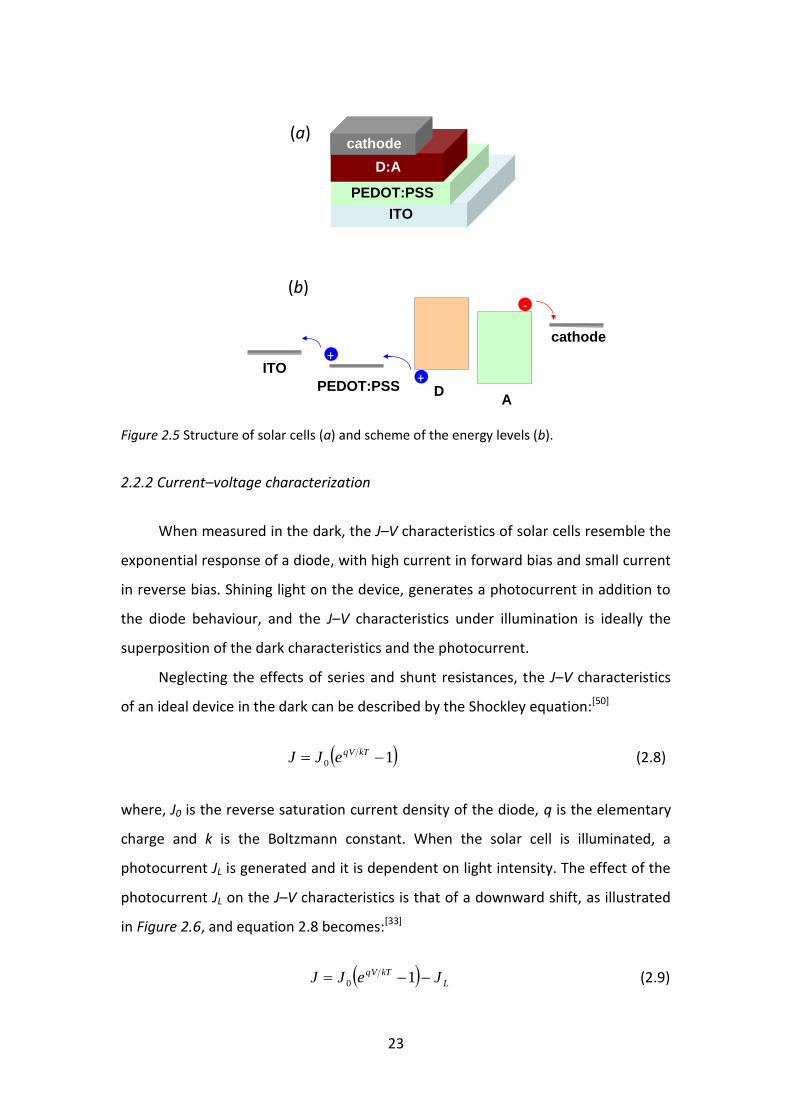
the scheme of the energy levels of the devices are shown in Figure 2.5.
23
ITO
PEDOT:PSS
D:A
cathode
PEDOT:PSS
cathode
D
(a)
(b)
ITO
A
+
+
-
Figure 2.5 Structure of solar cells (a) and scheme of the energy levels (b).
2.2.2 Current–voltage characterization
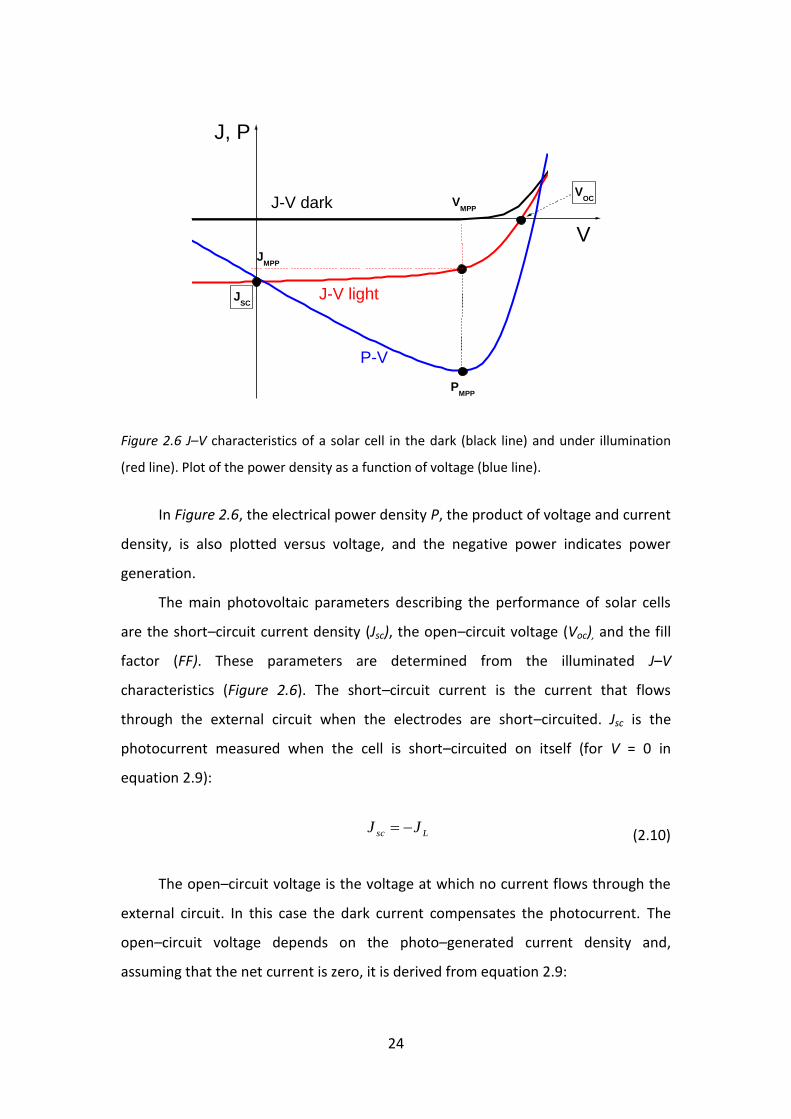
When measured in the dark, the J–V characteristics of solar cells resemble the
exponential response of a diode, with high current in forward bias and small current
in reverse bias. Shining light on the device, generates a photocurrent in addition to
the diode behaviour, and the J–V characteristics under illumination is ideally the
superposition of the dark characteristics and the photocurrent.
Neglecting the effects of series and shunt resistances, the J–V characteristics
of an ideal device in the dark can be described by the Shockley equation:[50]
10 kTqVeJJ (2.8)
where, J0 is the reverse saturation current density of the diode, q is the elementary
charge and k is the Boltzmann constant. When the solar cell is illuminated, a
photocurrent JL is generated and it is dependent on light intensity. The effect of the
photocurrent JL on the J–V characteristics is that of a downward shift, as illustrated
in Figure 2.6, and equation 2.8 becomes:[33]
L
kTqV JeJJ 10 (2.9)
(a)
(b)
24
P-V
J-V light
J-V darkV
OC
JSC
VJ
MPP
VMPP
PMPP
J, P
Figure 2.6 J–V characteristics of a solar cell in the dark (black line) and under illumination
(red line). Plot of the power density as a function of voltage (blue line).
In Figure 2.6, the electrical power density P, the product of voltage and current
density, is also plotted versus voltage, and the negative power indicates power
generation.
The main photovoltaic parameters describing the performance of solar cells
are the short–circuit current density (Jsc), the open–circuit voltage (Voc), and the fill
factor (FF). These parameters are determined from the illuminated J–V
characteristics (Figure 2.6). The short–circuit current is the current that flows
through the external circuit when the electrodes are short–circuited. Jsc is the
photocurrent measured when the cell is short–circuited on itself (for V = 0 in
equation 2.9):
Lsc JJ (2.10)
The open–circuit voltage is the voltage at which no current flows through the
external circuit. In this case the dark current compensates the photocurrent. The
open–circuit voltage depends on the photo–generated current density and,
assuming that the net current is zero, it is derived from equation 2.9:
25
1ln
0J
J
q
kTV L
oc
(2.11)
The operation regime of a solar cell is not, however, neither under
open–circuit nor under short–circuit condition, but it is connected to an external
load to which provides an electrical power. The maximum power (PMPP = JMPPVMPP)
that the cell can deliver is related to the fill factor of the device, defined as:
ocsc
MPP
VJ
PFF
(2.12)
The power conversion efficiency, , usually expressed in percentage, is defined
as the ratio between the generated maximum electrical power and the incident light
power (Pin):
in
ocsc
in
MPP
P
FFVJ
P
P
(2.13)
Since is dependent on both temperature and light power, solar cells are
characterized in terms defined by a standard. For terrestrial applications the
standard includes: temperature of 25 °C; a white light source with a spectral
distribution AM1.5G, that is that of solar irradiance with the sun 45 ° above the
horizon; the density of the incident light power of 100 mW cm-2.
The photovoltaic parameters are obviously closely related to the electronic
properties of the active layer of the cell. Jsc is mainly determined by the number of
absorbed photons, and the efficiency of dissociation of photo–generated excitons
into pairs of free charges. Voc is a thermodynamic parameter mainly related to the
energy difference between the LUMO of the acceptor and the HOMO of the
donor.[51,52] The value of fill factor is significantly dependent on charge transport
properties in the D/A blend and on charge recombination processes.
The density of the light power incident on the cells was varied from a few
mW cm-2 to 100 mW cm-2 by using a set of quartz neutral filters to attenuate the
light beam from the sun simulator, calibrated at 100 mW cm-2.
26
2.2.3 Analysis of photocurrents
For the analysis of photocurrents, the J–V characteristics is recorded by
applying a voltage scan from a positive value, higher than Voc, towards negative
potentials. The density of the net photocurrent, Jph, is given by:
DLph JJJ (2.14)
where JD is the current density registered under dark conditions. Jph is usually
plotted, changed in sign, as a function of the effective voltage V0 – V (Figure 2.7),
where V is the applied voltage and V0, the compensation voltage, is defined as
Jph(V0) = 0.
intermediate effective
applied voltage
high effective applied voltage:
saturation
Vsat
Jsat
Jph
V0-V
Figure 2.7 Typical plot of the net photocurrent as a function of the effective voltage.
At high effective voltages, i.e. at high reverse applied voltages or at high
internal field, the photocurrent can saturate. In case of saturation, it is possible to
calculate the maximum generation rate (Gmax) of free electron–hole (e–h) pairs at
the D/A interface by using the simple relation:[53]
dqGJ maxsat (2.15)

27
where Jsat is the saturation photocurrent. In the saturation regime, all bound e–h
pairs (CT states at the D/A interface) are separated into free charge carriers and
consequently Gmax is only governed by the amount of absorbed photons.
Being aware of Gmax, it is possible to estimate the generation rate of free e–h
pair for any applied voltage, G(V), using the simple proportion:
VVJ
J
)V(G
G
ph
satmax
0
(2.16)
The dependence of Jph on the effective voltage at low internal field is mainly
governed by the competition between diffusion and drift current and Jph scales
linearly with V0–V. For intermediate and higher internal fields, Jph may show a
square–root dependence on the effective voltage. Such square–root behaviour is
typically explained in terms of a space–charge–limited (SCL) or a –limited model,
where is the lifetime of free charge carriers before their recombination.[54] The first
type of limitation of Jph typically occurs when the difference between the electron
and the hole mobility in the D/A blend exceeds one order of magnitude (strongly
unbalanced transport), leading to the accumulation of the slowest carriers in the
device. The fingerprints of the SCL–limited Jph are the ¾ power law dependence on
the light power:
VVPJ inph 0
75.0 (2.17)
and a clear dependence on Pin of Vsat, Vsat being the saturation voltage at which Jph
starts to saturate (Figure 2.6).
Differently, in the –limited case a too short carrier lifetime or a too low
mobility limits the photocurrent, which linearly scales with Pin:
VVPJ inph 0 (2.18)
and Vsat is roughly independent of the light intensity.
28
A voltage scan from 1.4 V to –12 V was applied to the cells and the light
intensity was varied as described in the previous paragraph.
2.2.4 Impedance spectroscopy
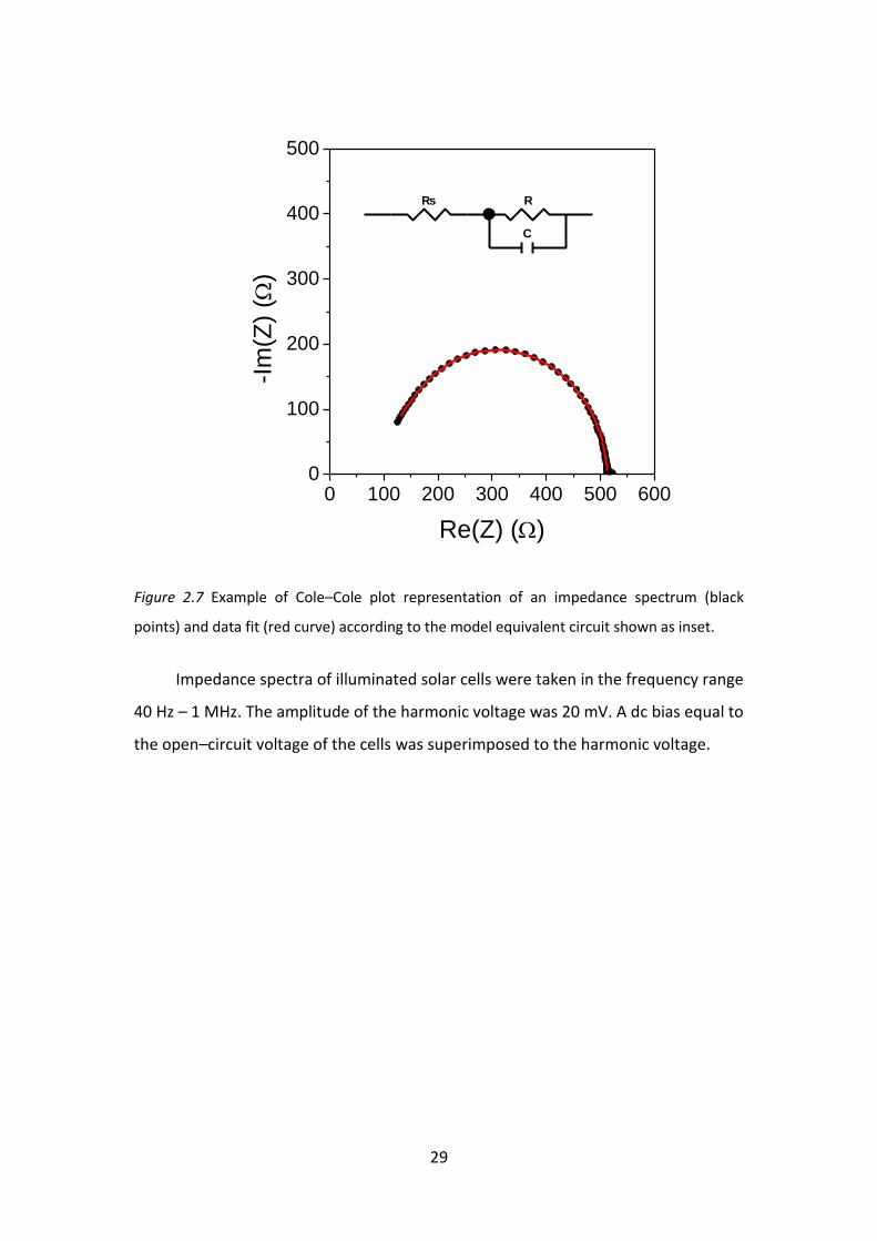
Impedance spectroscopy is a complex but very powerful tool, with many
applications in the field of materials science.[48] It is used to investigate relaxation
phenomena of charge carriers and, when applied to solar cells, it permits the
evaluation of charge carrier lifetime.[55] Impedance spectroscopy can also reveals
charge trapping phenomena in the D/A blends.[56]
The impedance of the system, stimulated by an harmonic voltage as described
in paragraph 2.1.3, and given by :
ZImiZRe
i
vZ
ac
ac (2.19)
is monitored as a function of frequency. The impedance spectrum is usually
represented with the imaginary part of Z plotted against the real part of Z
(Cole–Cole or Nyquist plot), with the frequency as the implicit variable.
The impedance spectrum is modelled on the basis of an equivalent circuit able
to account for the electrical behaviour of the device. Each resistor or capacitor
composing the equivalent circuit has a precise chemical/physical meaning,
connected with the behaviour of the device under test. The values of the circuit
elements are provided by the fit of the experimental data according to the model
circuit, and their combinations leads to relevant parameters for the behaviour of the
device (as lifetime of charge carriers, for solar cells). A simple example of an
impedance spectrum in the Cole–Cole representation, together with the related
equivalent circuit, is shown in Figure 2.7.
29
0 100 200 300 400 500 6000
100
200
300
400
500
-Im
(Z)
()
Re(Z) ()
Figure 2.7 Example of Cole–Cole plot representation of an impedance spectrum (black
points) and data fit (red curve) according to the model equivalent circuit shown as inset.
Impedance spectra of illuminated solar cells were taken in the frequency range
40 Hz – 1 MHz. The amplitude of the harmonic voltage was 20 mV. A dc bias equal to
the open–circuit voltage of the cells was superimposed to the harmonic voltage.
Rs R
C
Element Freedom Value Error Error %
Rs Fixed(X) 0 N/A N/A
R Fixed(X) 0 N/A N/A
C Fixed(X) 0 N/A N/A
Data File: D:\Nadia\Documenti\ENI 2008-2011\Solar cells\30258\Solar cells and IS 30258-022_C70BM\Ottobre 2011\IS 96.2% aging\S112J_IS_96.2%\S1giorno0.DAT
Circuit Model File: C:\Documents and Settings\Nadia\Desktop\AS celle vs Pin\P3HT-PCBM 28July11\Sample 18\AS\Parallel RC + R series.mdl
Mode: Run Simulation / Freq. Range (0.001 - 1000000)
Maximum Iterations: 100
Optimization Iterations: 0
Type of Fitting: Complex
Type of Weighting: Calc-Modulus

30
CHAPTER 3 – CHARGE TRANSPORT IN ANTHRACENE-
CONTAINING POLY ((P-PHENYLENE-ETHYNYLENE)-ALT-
POLY (P-PHENYLENE-VINYLENE))S
This chapter is dedicated to the investigation of charge transport proprieties
in a series of anthracene–containing poly((p–phenylene–ethynylene)–alt–poly(p–
phenylene–vinylene))s (PPE–PPVs), denoted AnE–PVs. AnE–PVs, with the
anthracene unit between two triple bonds, are a relevant class of conjugated
polymers,[57] exhibiting outstanding optoelectronic properties. Light–emitting diodes
showing a turn–on voltage below 2 V[58] and solar cells exhibiting a state–of–art
efficiency of around 5%, for PPV–based materials, have been already demonstrated
for this class of conjugated polymers.[59] The advantage of the triple bond in the
polymer structure, due to its cylindrical symmetry, is the preservation of the
conjugation between aromatic groups in case of rotation of the aromatic plane,
though it is maximum in the planar conformation.[60, 61] It has been shown that
PPE–PPVs are characterized by an enhancement of both backbone stiffness and
electron affinity, as compared to parent PPV, due to the incorporation of the
electron–withdrawing ethynylene units into the polymer backbone.[62] Indeed, the
triple bond acts as a bridge for the electrons of two aromatic systems also by means
of –* hyperconjugation. In addition, this class of conjugated polymers shows a
good ambipolar charge transport behaviour, as discussed in paragraph 3.2.
Substituents can greatly affect the electronic properties of conjugated
polymers,[8,9] other than modifying their processability in organic solvents.
Depending on their nature, size and position, substituents can influence the
molecular packing of polymer chains, thus greatly affecting charge transport
properties of polymer films. So, the effect of lateral–chains on charge carrier
mobility of AnE–PVs was investigated.
The electronic properties of conjugated polymers are not simply dependent
on their chemical structure but are highly affected by macromolecular parameters,
such as molecular weight (MW) and polydispersity. Indeed, macromolecular
31
parameters are known to have great effects on the optical and charge transport
properties of conjugated polymer films, also through a different organization of
polymer chains in the solid state induced by different MW.[4, 5] A study of the effects
of a moderate variation of molecular weight on the transport properties (as well as
on the optical, structural, and morphological properties) was conducted for one of
the best–performing AnE–PV here considered. The investigation was extended to
the photovoltaic performance of the related BHJ solar cells made with [6,6]–phenyl–
C61–butyric acid methylester (PCBM) as electron–acceptor.
Another parameter which has a critical role for the transport properties of
polymer films is the organization of polymer chains, which can be affected by
post–deposition treatments.[63] The effect of a thermal treatment and of a solvent
treatment on charge carrier mobility was also investigated.
3.1 Materials
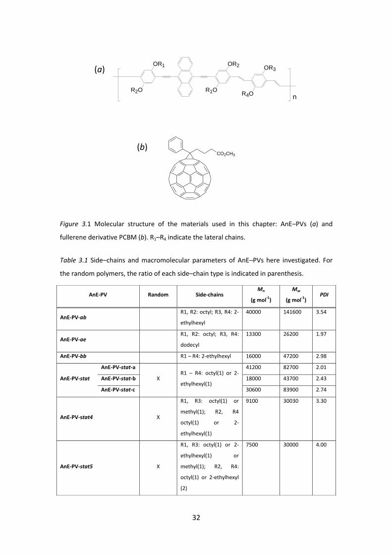
The chemical structure of the investigated AnE–PVs polymers is shown in
Figure 3.1a. They are characterized by the same conjugated backbone, but differ in
the nature of the grafted solubilising alkoxy side–chains (linear or branched), and
were prepared either with well–defined or with randomly distributed side–chains
(random polymers). Side–chains and macromolecular parameters (number–average
molecular weight, Mn, weight–average molecular weight, Mw, and polidispersity
index, PDI) of AnE–PVs here investigated, are collected in Table 3.1. In the case of
AnE–PV–stat, three different samples were considered with different
macromolecular parameters.
The polymers were synthesized at the Linz Institute for Organic Solar Cells,
Johannes Kepler University of Linz, according to procedures already reported in the
literature.[57, 58, 60] Their HOMO/LUMO levels, electrochemically determined, are
– 5.09 eV and – 3.04 eV, respectively.[64]
PCBM was purchased from Sigma–Aldrich.
32
nR2O
OR1 OR2
R1O
OR3
R4O
(a)
CO2CH3
(b)
Figure 3.1 Molecular structure of the materials used in this chapter: AnE–PVs (a) and
fullerene derivative PCBM (b). R1–R4 indicate the lateral chains.
Table 3.1 Side–chains and macromolecular parameters of AnE–PVs here investigated. For
the random polymers, the ratio of each side–chain type is indicated in parenthesis.
AnE-PV Random Side-chains Mn
(g mol-1
)
Mw
(g mol-1
) PDI
AnE-PV-ab R1, R2: octyl; R3, R4: 2-
ethylhexyl
40000 141600 3.54
AnE-PV-ae R1, R2: octyl; R3, R4:
dodecyl
13300 26200 1.97
AnE-PV-bb R1 – R4: 2-ethylhexyl 16000 47200 2.98
AnE-PV-stat
AnE-PV-stat-a
X R1 – R4: octyl(1) or 2-
ethylhexyl(1)
41200 82700 2.01
AnE-PV-stat-b 18000 43700 2.43
AnE-PV-stat-c 30600 83900 2.74
AnE-PV-stat4 X
R1, R3: octyl(1) or
methyl(1); R2, R4
octyl(1) or 2-
ethylhexyl(1)
9100 30030 3.30
AnE-PV-stat5 X
R1, R3: octyl(1) or 2-
ethylhexyl(1) or
methyl(1); R2, R4:
octyl(1) or 2-ethylhexyl
(2)
7500 30000 4.00

33
3.2 Ambipolar behaviour
For the first time, the excellent ambipolar charge transport behaviour of
AnE–PVs was reported. The ambipolar transport ability was first demonstrated for
AnE–PV–stat–a, then confirmed for the other investigated AnE–PVs, as shown in the
next paragraphs.
AnE–PV–stat–a is capable of both easy oxidation and reduction, as
demonstrated by the reversible oxidation and reduction peaks observed in its cyclic
voltammogram,[64] this being a prerequisite for ambipolar transport. A further
evidence for ambipolar transport ability was given by the
electron–state–distribution of the HOMO/LUMO levels of AnE–PVs, computed by
B3LYP/6-31G*[65] density functional theory, which shows a very good delocalization
of both energy levels (Figure 3.2).
Figure 3.2 HOMO/LUMO electron density plots calculated by B3LYP/6-31G* for the
energy–minimized model structure of the methoxy–substituted trimer.
Charge transport was investigated by using the TOF technique. For a better
comparison, hole and electron mobility were obtained from TOF measurements
made on the same device, with the structure ITO/AnE–PV–stat–a/Al (18 nm). The
polymer film (3.6 m thick) was deposited by drop–casting from
1,2–dichlorobenzene solution (30 g L-1).
A typical photocurrent transient for holes is shown in Figure 3.3a, for an
applied field of 4.2×10⁴ V cm-1. Transport of holes is not affected by high dispersion
LUMO
HOMO
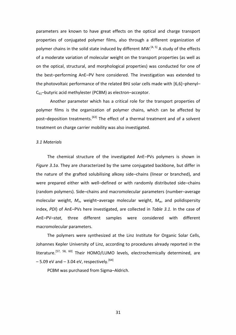
34
in cast–films of AnE–PV–stat–a and the transit time of carriers can be detected also
in a linear scale, mainly at higher fields. The low dispersion of TOF signals is
consistent with the multi–crystalline character of this copolymer.[66] By reversing the
polarity of the illuminated semitransparent Al electrode, the signal reported in
Figure 3.3b was observed for electrons, clearly showing that current due to negative
carriers decreases more rapidly and indicating that the time required for electrons
to travel through the same sample is much shorter than that for holes.
0.0 5.0x10⁻⁵
1.0x10⁻⁴
0.0 5.0x10⁻⁵
1.0x10⁻⁴
(a)
Electrons
Holes
Ph
oto
cu
rre
nt
(a.
u.)
(b)
Time (s)
Ph
oto
cu
rre
nt
(a.
u.)
Figure 3.3 Linear plots of photocurrent signals for an ITO/AnE–PV–stat–a /Al device with the
illuminated semitransparent Al electrode: positively biased (a) and negatively biased (b). In
both cases, the applied field was 4.2×10⁴ V cm-1.
35
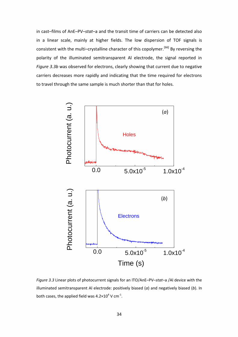
The comparison of the two signals of Figure 3.3 confirms the usual finding that
transport of electrons is more dispersed than that of positive carriers in conjugated
polymers,[67] commonly attributed to trapping effects. Indeed, with the LUMO level
at –3.04 eV,[62] electron transport states of AnE–PV–stat–a are expected to lie close
to the typical impurities acting as trapping states for negative carriers.[68] However,
though the dispersion of photocurrent signals, two different slopes were clearly
observed also for electrons in the double–logarithmic representation, as shown in
Figure 3.4, with slopes far below –1 for times shorter than ttr and much higher than
–1 for longer times and whose sum was very close to –2, as predicted by the
Scher–Montroll theory.[69] Both for electron and hole TOF signals, charge carrier
transit times were determined from the intersection point between the two straight
lines with different slopes.
Figure 3.4 The same signals of Figure 3.3 shown in a double–logarithmic scale. The values of
the slopes before and after the transit time are also indicated in the case of electrons.
10-6
10-5
10-4
1.57
0.38
Photo
curr
ent (a
.u.)
Time (s)
Electrons Holes

36
The values of charge carrier mobility were calculated through the well–known
expression of Equation 2.4, and are plotted as a function of the square–root of E in
Figure 3.5.
Figure 3.5 Room–temperature TOF mobility as a function of the square–root of field for an
as–cast AnE–PV–stat–a film 3.6 m thick. The lines indicate the linear fit to the experimental
data.
Differently from other good ambipolar conjugated polymers already reported
in the literature, the bulk electron mobility (e) in as–cast AnE–PV–stat–a films is
roughly six times higher than hole mobility (h) in the investigated range of field. For
example, at the same field of 1.1×10⁵ V cm-1, an electron mobility of
1.2×10⁻³ cm2 V-1 s-1 was calculated, against 2.0×10⁻⁴ cm2 V-1 s-1 for holes. Both for
electron and hole mobility, a good linear trend of with E1/2 was obtained (Figure
3.5), indicating a Poole–Frenkel behaviour (Equation 1.1). Such a behaviour has been
frequently observed in organic materials and could be attributed to the effects of
energetic and positional disorder on the hopping conduction in disordered
molecular solids.[18] The parameters for the Poole–Frenkel fit to mobility data of
100 200 300 400 500
10-4
10-3
Electrons
Holes
Mobili
ty (
cm
2 V
-1 s
-1)
E1/2
(V cm-1)1/2
37
Figure 3.5 are 0e = 3.9×10⁻⁴ cm2 V-1 s-1 and = 3.4×10⁻³ (V cm-1)-1/2 for electrons and
0h = 7.9×10⁻⁵ cm2 V-1 s-1 and = 3.1×10⁻³ (V cm-1)-1/2 for holes. The values of are
rather usual for conjugated polymers and indicate a moderate field–dependence of
charge carrier mobility in AnE–PV–stat–a. That of electron mobility is however a bit
stronger than that for holes, consistent with increased/different trapping
processes.[70]
3.3 Effect of side–chains
The investigation of hole and electron mobility by TOF was extended to the
other five AnE–PVs with different side–chains (Table 3.1).
Given that transport of charge carriers is highly affected by the organization of
polymers chains in the solid state,[71, 72] the same conditions (solvent, deposition
method, post–deposition treatment) were used for the deposition of all polymer
films, that is those already described in paragraph 3.2 for AnE–PV–stat–a. The
thickness of the polymer layers was 9.4, 1.4, 2.9, 7.0 and 15.5 m for AnE–PV–ab,
AnE–PV–ae, AnE–PV–bb, AnE–PV–stat4, and AnE–PV–stat5, respectively.
Typical photocurrent transients, both for holes and electrons, are displayed in
Figure 3.6 in a double–logarithmic representation and for a comparable applied
electric field of about 1×10⁵ V cm-1. The inspection of Figures 3.6a–3.6f indicates
that all AnE–PVs investigated show an ambipolar charge transport, though much
more dispersed for negative carriers.
By plotting the logarithm of mobility as a function of the square–root of E, a
good linear trend was obtained in most cases, as shown in Figure 3.7. The
parameters obtained from the Poole–Frenkel fit to mobility data of Figure 3.7 are
collected in Table 3.2.
38
Figure 3.6 Typical TOF signals in log–log scales for an applied electric field of about
1×10⁵ V cm-1. Positive carriers (red lines) and negative carriers (blue lines).
10-6
10-5
10-6
10-5
10-4
10-6
10-5
10-5
10-4
10-3
10-4
10-3
10-2
10-5
10-4
(c)
AnE-PV-bb
AnE-PV-aeAnE-PV-ab
Time (s)
(b)(a)
Time (s)
(d)
AnE-PV-stat-a
Time (s)
(f)
AnE-PV-stat5
Time (s)
(e)
AnE-PV-stat4
Time (s)
Time (s)
39
200 400 600 800
10-6
10-5
10-4
10-3
200 400 600 800
10-6
10-5
10-4
10-3
10-2
(a)
h (
cm
2 V
-1 s
-1)
E1/2
(V cm-1)
/1/2
(b)
e (
cm
2 V
-1 s
-1)
E1/2
(V cm-1)
/1/2
Figure 3.7 Hole mobility (filled symbol) (a) and electron mobility (open symbol) (b) as a
function of the square–root of the electric field for: AnE–PV–ab (green up triangles);
AnE–PV–ae (orange stars); AnE–PV–bb (blue squares); AnE–PV–stat–a (red circles);
AnE–PV–stat4 (violet down triangles); AnE–PV–stat5 (magenta diamonds). The lines are the
linear fit to the experimental data.
40
Table 3.2. Summary of mobility data: hole and electron mobility for an applied electric field
of about 1×10⁵ V cm-1, zero–field mobility and Poole–Frenkel for holes and electrons.
AnE-PV ab ae bb stat-a stat4 stat5
Side-chains
octyl,
2-ethylhexyl
octyl,
dodecyl
2-
ethylhex
yl
octyl,
2-ethylhexyl
octyl
2-
ethylhexyl,
methyl
octyl,
2-
ethylhexy
l, methyl
h
(cm2 V-1 s-1) 1.3×10⁻⁴ 8.2×10⁻⁶ 2.3×10⁻⁴ 2.0×10⁻⁴ 1.6×10⁻⁶ 4.0×10⁻⁵
0 h
(cm2 V-1 s-1) 3.3×10⁻⁵ 3.8×10⁻⁶ 7.9×10⁻⁵ 7.9×10⁻⁵ 3.0×10⁻⁷ 1.3×10⁻⁵
h
(V cm-1)-1/2 4.3×10⁻³ 1.6×10⁻³ 3.4×10⁻³ 3.1×10⁻³ 5.1×10⁻³ 3.6×10⁻³
e
(cm2 V-1 s-1) 2.9×10⁻⁴ 1.6×10⁻⁵ 9.1×10⁻⁴ 1.2×10⁻³ 5.0×10⁻⁶ 4.1×10⁻⁵
0e
(cm2 V-1 s-1) 6.7×10⁻⁵ 1.5×10⁻⁵ n.a. 3.9×10⁻⁴ 1.3×10⁻⁶ 1.1×10⁻⁵
e
(V cm-1)-1/2 4.4×10⁻³ 6.7×10⁻⁴ n.a. 3.4×10⁻³ 4.1×10⁻³ 4.2×10⁻³
The only decreasing trend with E was observed for electron mobility, in
AnE–PV–bb films (Figure 3.7b). However, both the Poole–Frenkel–like trend of
mobility, and a decreasing trend of with E can be explained within the same
model of an hopping conduction, as demonstrated by Monte Carlo simulations.[73, 74]
The data of Figure 3.7 and Table 3.2 clearly show the great effect of lateral
chains on charge carrier mobility of AnE–PVs, with varying by two orders of
magnitude both for holes (ranging between 1.6×10⁻⁶ and 2.3×10⁻⁴ cm2 V-1 s-1 for E of
about 105 V cm-1) and electrons (between 5.0×10⁻⁶ and 1.2×10⁻³ cm2 V-1 s-1 for the
same field). As expected, the polymer with the longest substituents (AnE–PV–ae,
with octyl and dodecyl chains) shows low mobility compared with the other ones,
consistent with the reduction of the electronic interaction between conjugated
backbones as the extension of lateral chains increases.[75, 76] This is also confirmed by
41
the comparison between AnE–PV–ab and AnE–PV–bb, only differing for the octyl
side–chains. The latter, with only 2–ethylexyl substituents, shows higher mobility
values (2.3×10⁻⁴ against 1.3×10⁻⁴ cm2 V-1 s-1 for holes, 9.1×10⁻⁴ against
2.9×10⁻⁴ cm2 V-1 s-1 for electrons, for field of about 105 V cm-1). However, the most
striking difference of AnE–PV–ae, compared with the other polymers, is represented
by the low dependence of mobility on electric field, as demonstrated by the lowest
values of (Table 3.2). This could be due to a lower energetic disorder[77] in the
fluctuation of the energy of the hopping sites for charge transport, which could be
attributed to a more ordered arrangement of polymer chains in the film. Indeed, a
layered structure consisting of – stacked backbones has been already reported for
films made of AnE–PVs with all–linear side chains attached close to the
anthracenylene–ethynylene unit, in contrast to the more amorphous structure of
polymers with branched lateral chains attached to the same backbone[66]. The other
five polymers, all bearing branched 2–ethylhexyl chains, show a value ranging
between 3.1×10⁻³ and 5.1×10⁻³ cm1/2 V-1/2, without a clear trend with the molecular
structure.
The comparison between statistical and non–statistical polymers can be done
by considering AnE–PV–ab and AnE–PV–stat–a, bearing the same octyl and
2–ethylhexyl side–chains. Better values both for mobility and were obtained for
the polymer with lateral chains statistically distributed, confirming the superior
features of the random polymer compared to the counterpart based on
well–defined side–chain.[64] Finally, looking at the data of Table 3.2, it is surprising
the difference of roughly one order of magnitude between the mobility values of
AnE–PV–stat4 and AnE–PV–stat5, two random polymers with the same side–chains
and just differing for the different amount of short methyl chains. The former, with
more methyl groups in the molecular structure (Table 3.1), shows lower values
compared with AnE–PV–stat5, as well as the lowest one for the six considered
polymers, indicating that the short methyl chains have a detrimental effect on the
transport properties of charge carriers.
It is worth noting that the two polymers with methyl side–chains are among the
ones exhibiting the lowest mobilities (Figure 3.7 and Table 3.2) of the six considered,
42
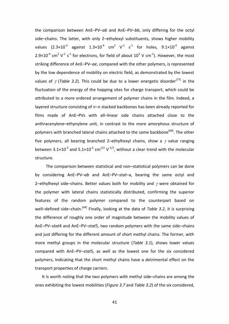
confirming that the shortest lateral chains prevent a favourable organization of
polymer films for the transport of charge carriers. To support this hypothesis, the
X–Ray Diffraction (XRD) pattern of AnE–PV–stat4 film is compared to that of
AnE–PV–stat–a, without methyl chains and showing very good mobility values. The
polymer films, prepared in the same conditions used for mobility investigation,
showed very different XRD patterns (Figure 3.8).
AnE-PV-stat-a
AnE-PV-stat4
Figure 3.8 XRD spectra for AnE–PV–stat–a and AnE–PV–stat4 films deposited onto
zero–background quartz.
Differently from AnE–PV–stat–a, showing a semicrystalline character,
AnE–PV–stat4 reveals its complete amorphous feature. Indeed, AnE–PV–stat–a
sample shows a crystalline peak at 5.53° (2), corresponding to a staking interlayer
distance of 1.53 nm, while only a bell–shaped profile is visible in the wide angle
region of the XRD pattern of AnE–PV–stat4, also present in the pattern of
AnE–PV-stat–a and related to the amorphous component of the investigated films.
Likely, the short methyl side–chains, reducing the overall rough symmetry of the
repeating unit, could hinder the possibility of a regular stacking of the polymer main
chains. This leads to a very different organization in the solid state and highly affects
the charge transport properties of the films made with the two different polymers,
with a variation of two orders of magnitude in the mobility values. It is important to
43
underline that also the photophysical properties of the two statistical polymers are
greatly influenced, with AnE–PV–stat–a showing improved absorption and emission
spectra compared to the amorphous AnE–PV–stat4.[58]
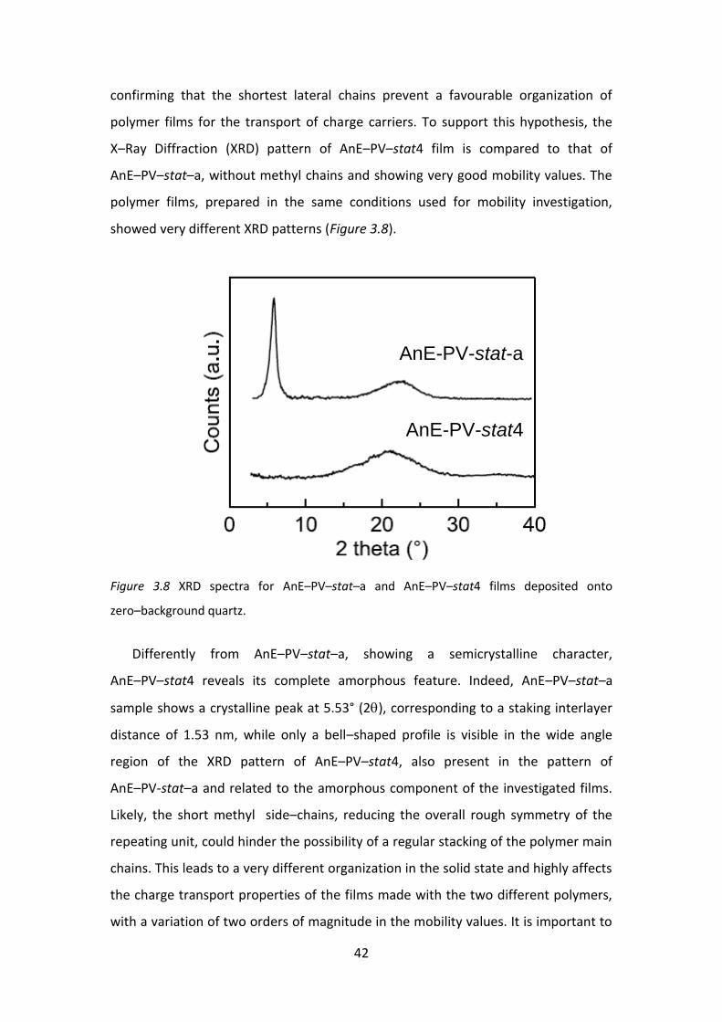
The very different transport properties of AnE–PV–stat–a and AnE–PV–stat4
could be also attributed to a different extent of charge trapping processes. In this
case, a different trend of charge carrier transit times with the applied electric field
should be observed. It has been shown that, in a multiple trapping model, the transit
time of charge carriers exhibits the following electric field dependence[78]
1 EEttr (3.1)
where is a dispersion parameter (0 < < 1; = 1 for non dispersive transport)
introduced by Scher and Montroll[79] in their model for the description of dispersive
transport in amorphous solids. The electric field dependence of transit times derived
from the TOF measurements are reported in Figure 3.9 for AnE–PV–stat–a and
AnE–PV–stat4.
104
105
10-6
10-5
10-4
10-3
10-2
= 0.71
= 0.55 = 0.68
= 0.57
t tr (
s)
E (V cm-1)
AnE-PV-stat-a - holes
AnE-PV-stat4 - holes
AnE-PV-stat-a - electrons
AnE-PV-stat4 - electrons
Figure 3.9 Transit time of holes (filled symbols) and electrons (open symbols) as a function
of the electric field for AnE–PV–stat–a (red circles) and AnE–PV–stat4 (violet down
triangles).
44
From the slope of the lines representing the linear fit to the experimental data,
the values of the dispersion parameter were extracted. 0.57 and 0.55 were obtained
for AnE–PV–stat4, for holes and electrons respectively, compared with the expected
higher values for of 0.68 (holes) and 0.71 (electrons) calculated for AnE–PV–stat–a
and indicating that charge transport is less affected by charge trapping events in this
latter polymer.
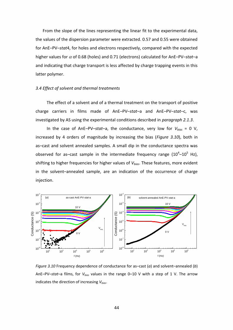
3.4 Effect of solvent and thermal treatments
The effect of a solvent and of a thermal treatment on the transport of positive
charge carriers in films made of AnE–PV–stat–a and AnE–PV–stat–c, was
investigated by AS using the experimental conditions described in paragraph 2.1.3.
In the case of AnE–PV–stat–a, the conductance, very low for Vbias = 0 V,
increased by 4 orders of magnitude by increasing the bias (Figure 3.10), both in
as–cast and solvent annealed samples. A small dip in the conductance spectra was
observed for as–cast sample in the intermediate frequency range (104–105 Hz),
shifting to higher frequencies for higher values of Vbias. These features, more evident
in the solvent–annealed sample, are an indication of the occurrence of charge
injection.
Figure 3.10 Frequency dependence of conductance for as–cast (a) and solvent–annealed (b)
AnE–PV–stat–a films, for Vbias values in the range 0–10 V with a step of 1 V. The arrow
indicates the direction of increasing Vbias.
102
103
104
105
106
10-8
10-7
10-6
10-5
10-4
10-3
10-2
(a) as-cast AnE-PV-stat-a
Vbias
10 V
0 V
Co
nd
ucta
nce
(S
)
f (Hz)
102
103
104
105
106
10-8
10-7
10-6
10-5
10-4
10-3
10-2
(b) solvent-annealed AnE-PV-stat-a
Vbias
0 V
10 V
Co
nd
ucta
nce
(S
)
f (Hz)
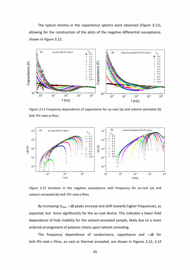
45
The typical minima in the capacitance spectra were observed (Figure 3.11),
allowing for the construction of the plots of the negative differential susceptance,
shown in Figure 3.12.
Figure 3.11 Frequency dependence of capacitance for as–cast (a) and solvent–annealed (b)
AnE–PV–stat–a films.
Figure 3.12 Variation in the negative susceptance with frequency for as–cast (a) and
solvent–annealed (b) AnE–PV–stat-a films.
By increasing Vbias, –B peaks increase and shift towards higher frequencies, as
expected, but more significantly for the as–cast device. This indicates a lower field
dependence of hole mobility for the solvent-annealed sample, likely due to a more
ordered arrangement of polymer chains upon solvent annealing.
The frequency dependence of conductance, capacitance and –B for
AnE–PV–stat–c films, as–cast or thermal annealed, are shown in Figures 3.13, 3.14
102
103
104
105
106
10-9
(a) Vbias
0 V
1 V
2 V
3 V
4 V
5 V
6 V
7 V
8 V
9 V
10 V
as-cast AnE-PV-stat-a
Capacitance (
F)
f (Hz)
102
103
104
105
106
10-9
(b) Vbias
0 V
1 V
2 V
3 V
4 V
5 V
6 V
7 V
8 V
9 V
10 V
solvent-annealed AnE-PV-stat-a
Ca
pacita
nce
(F
)f (Hz)
103
104
105
10-8
10-7
10-6
10-5
10-4 (a)
Vbias
2 V
3 V
4 V
5 V
6 V
7 V
8 V
9 V
10 V
as-cast AnE-PV-stat-a
-B
(S
)
f (Hz)
102
103
104
105
106
10-8
10-7
10-6
10-5
10-4 (b)
Vbias
2 V
3 V
4 V
5 V
6 V
7 V
8 V
9 V
10 V
solvent-annealed AnE-PV-stat-a
-B
(S
)
f (Hz)
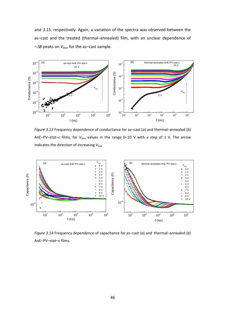
46
and 3.15, respectively. Again, a variation of the spectra was observed between the
as–cast and the treated (thermal–annealed) film, with an unclear dependence of
–B peaks on Vbias for the as–cast sample.
Figure 3.13 Frequency dependence of conductance for as–cast (a) and thermal–annealed (b)
AnE–PV–stat–c films, for Vbias values in the range 0–10 V with a step of 1 V. The arrow
indicates the direction of increasing Vbias.
Figure 3.14 Frequency dependence of capacitance for as–cast (a) and thermal–annealed (b)
AnE–PV–stat–c films.
102
103
104
105
106
10-8
10-7
10-6
10-5
10-4
10-3 (a) as-cast AnE-PV-stat-c
Vbias
10 V
0 V
Conducta
nce (
S)
f (Hz)
101
102
103
104
105
106
10-7
10-6
10-5
10-4
10-3 (b) thermal-annealed AnE-PV-stat-c
Vbias
10 V
0 V
f (Hz)
Conducta
nce (
S)
102
103
104
105
106
10-9
(a) Vbias
0 V
1 V
2 V
3 V
4 V
5 V
6 V
7 V
8 V
9 V
10 V
as-cast AnE-PV-stat-c
Ca
pa
cita
nce
(F
)
f (Hz)
102
103
104
105
106
10-9
Vbias
(b)
0 V
1 V
2 V
3 V
4 V
5 V
6 V
7 V
8 V
9 V
10 V
thermal-annealed AnE-PV-stat-c
Capacitance (
F)
f (Hz)

47
Figure 3.15 Variation in the negative susceptance with frequency for as–cast (a) and
thermal–annealed (b) AnE–PV–stat–c films.
The values of the transit time of holes were extracted from the frequencies
corresponding to the –B peaks, as described in paragraph 2.1.3, and hole mobility
was calculated by using the well–known expression (equation 1.1).
Figure 3.16 Dependence of hole mobility on the square–root of the electric field for
as–cast and solvent–annealed AnE–PV–stat–a (a) and as–cast and thermal–annealed
AnE–PV–stat–c (b) films. The dotted lines represent the linear fit to the experimental data.
As shown in Figure 3.13, the mobility data plotted against the square–root of
the electric field, show a linear trend, suggesting a Poole–Frenkel behaviour for all
the devices here considered. The parameters extracted from the Poole–Frenkel are
collected in Table 3.3.
102
103
104
105
10-8
10-7
10-6
10-5
10-4
Vbias
(a)
2 V
3 V
4 V
5 V
6 V
7 V
9 V
10 V
as-cast AnE-PV-stat-c
(S
)
f (Hz)
103
104
105
106
10-8
10-7
10-6
10-5
10-4
(b) Vbias
2 V
3 V
4 V
5 V
6 V
7 V
8 V
9 V
10 V
thermal-annealed AnE-PV-stat-c
S
f (Hz)
150 200 250 300 350 400 450 500
10-5
10-4
(b)AnE-PV-stat-c
as cast
thermal annealed
h (
cm
2 V
-1 s
-1)
E1/2
(V cm-1)
1/2
200 250 300 350 400 450 500
10-5
10-4
(a)AnE-PV-stat-a
as cast
solvent annealed
h (
cm
2 V
-1 s
-1)
E1/2
(V cm-1)
1/2

48
Table 3.3 Poole-Frenkel parameters for AnE-PV-stat-a and AnE-PV-stat-c samples and
mobility values calculated for a field of 105 V cm-1.
Polymer Treatment 0h
(cm2V-1s-1)
h
(V cm-1)1/2
h @105 V cm-1
(cm2V-1s-1)
AnE-PV-stat-a as-cast 3.04×10⁻⁶ 3.64×10⁻³ 9.61×10⁻⁶
solvent-annealed 1.75×10⁻⁵ 3.84×10⁻³ 5.89×10⁻⁵
AnE-PV-stat-c as-cast 7.65×10⁻⁶ 3.09×10⁻³ 2.01×10⁻⁵
thermal-annealed 5.64×10⁻⁶ 5.94×10⁻³ 3.69×10⁻⁵
Solvent and thermal annealing enhance the mobility of holes in
AnE–PV–stat–a and AnE–PV–stat–c films spin-coated from chloroform solutions,
likely due to an enhanced order upon annealing. Looking at the data of Table 3.3, it
is worth noting that the mobility at zero field decreased and the Poole–Frenkel
factor increased upon thermal–annealing AnE–PV–stat–c polymer film. In order to
shed light on the origin of the variations observed in the transport of holes,
AnE–PV–stat–c and AnE–PV–stat–a films, prepared and treated in the same
conditions used for admittance spectroscopy, were investigated by XRD (Figure
3.17).
Figure 3.17 XRD spectra for AnE–PV–stat–a and AnE–PV–stat–c films deposited onto
zero–background quartz.

49
In both cases the XRD profiles of the annealed samples suggest an increase in
the molecular organization, but only in the case of thermal–annealed
AnE–PV–stat–c sample the order is meaningful. We can appreciate an intense peak
at 5.4° (d=1.64nm), two very low at 10.8° and 16.5° (0.82 and 0.54 nm) and a broad
‘bump’ centred around 22.6°. The peaks are due to the first, second and third order
of a 1.64 nm periodicity due to chain–chain interlayer distance. The broad halo is
caused by the disordered stacking of the chains within the main chain layers. For
samples AnE–PV–stat–c as–cast and AnE–PV–stat–a solvent–annealed, only the
reflection at about 5.8° is detected with low intensity, suggesting a low fraction of
ordered material.
In summary, as-cast films from chloroform solutions are characterized by a low
order degree, enhanced, as expected, by annealing. The thermal–annealed
AnE–PV–stat–c sample shows the highest order degree, though does not exhibit the
highest mobility. Indeed, though the significant difference of the XRD patters of
annealed AnE–PV–stat–c and AnE–PV–stat–a films, the highest mobility was
calculated for the less ordered solvent–annealed AnE–PV–stat–a. In addition, the
stronger field activation of mobility observed for thermal-annealed AnE–PV–stat–c
could indicate a hole transport limited by the grain boundaries of a multi–crystalline
structure, often observed for this class of polymers.[66]
AnE–PV–stat–a and AnE–PV–stat–c polymer samples mainly differ for PDI, the
weight average molecular weight being comparable (Table 3.1). Therefore, the light
differences observed for charge transport in the two polymer samples could be due
to their polydispersity, affecting the arrangement of polymer chains in the solid
state. The role of PDI for the film organization, as well as for charge transport, will
be confirmed in the next paragraph.
3.5 Effect of a fine variation of the macromolecular parameters
Three AnE–PV–stat polymer samples were considered, differing for the
macromolecular parameters, denoted AnE–PV–stat–a, AnE–PV–stat–b,
AnE–PV–stat–c (Table 3.1). The weight–average molecular weight (43700 g mol-1) of
AnE–PV–stat–b was nearly two times lower than that determined for
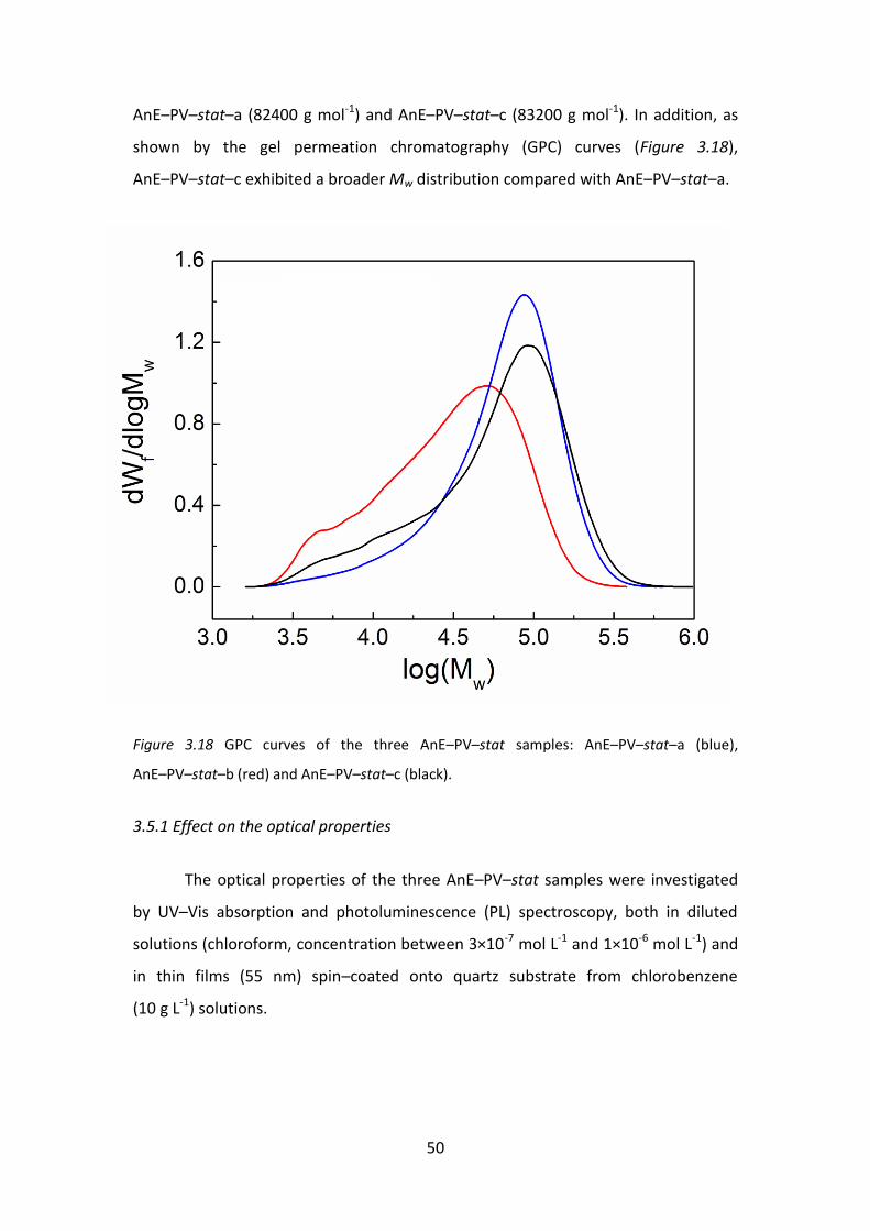
50
AnE–PV–stat–a (82400 g mol-1) and AnE–PV–stat–c (83200 g mol-1). In addition, as
shown by the gel permeation chromatography (GPC) curves (Figure 3.18),
AnE–PV–stat–c exhibited a broader Mw distribution compared with AnE–PV–stat–a.
Figure 3.18 GPC curves of the three AnE–PV–stat samples: AnE–PV–stat–a (blue),
AnE–PV–stat–b (red) and AnE–PV–stat–c (black).
3.5.1 Effect on the optical properties
The optical properties of the three AnE–PV–stat samples were investigated
by UV–Vis absorption and photoluminescence (PL) spectroscopy, both in diluted
solutions (chloroform, concentration between 3×10⁻⁷ mol L-1 and 1×10⁻⁶ mol L-1) and
in thin films (55 nm) spin–coated onto quartz substrate from chlorobenzene
(10 g L-1) solutions.
AnE-PV-stat-a
AnE-PV-stat-b
AnE-PV-stat-c
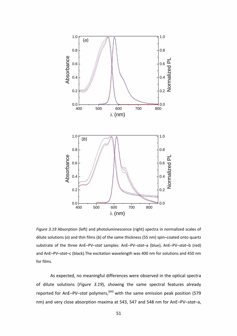
51
400 500 600 700 8000.0
0.2
0.4
0.6
0.8
1.0
0.0
0.2
0.4
0.6
0.8
1.0
(nm)
Abso
rba
nce
(a)
No
rma
lize
d P
L
400 500 600 700 8000.0
0.2
0.4
0.6
0.8
1.0
0.0
0.2
0.4
0.6
0.8
1.0
(nm)
Absorb
ance
(b)
Norm
aliz
ed P
L
Figure 3.19 Absorption (left) and photoluminescence (right) spectra in normalized scales of
dilute solutions (a) and thin films (b) of the same thickness (55 nm) spin–coated onto quartz
substrate of the three AnE–PV–stat samples: AnE–PV–stat–a (blue), AnE–PV–stat–b (red)
and AnE–PV–stat–c (black).The excitation wavelength was 400 nm for solutions and 450 nm
for films.
As expected, no meaningful differences were observed in the optical spectra
of dilute solutions (Figure 3.19), showing the same spectral features already
reported for AnE–PV–stat polymers,[64] with the same emission peak position (579
nm) and very close absorption maxima at 543, 547 and 548 nm for AnE–PV–stat–a,

52
AnE–PV–stat–b and AnE–PV–stat–c, respectively. Films of AnE–PV–stat spin–cast
from chlorobenzene solution are known to show a stacking behaviour,[64] resulting
in structured absorption and photoluminescence spectra exhibiting two peaks, as
shown in Figure 3.19, for the AnE–PV–stat samples here investigated. Given the
narrow molar mass range for the three polymer samples, significant variations of the
optical spectra were not observed, nevertheless some considerations can be made.
The main difference in the absorption spectra of films is between
AnE–PV–stat–a and the other two samples, the former showing the lower energy
peak slightly blue–shifted (located at 588 nm, against 586 and 579 nm for samples
AnE–PV–stat–c, and AnE–PV–stat–b, respectively), indicating a moderate reduction
of the effective conjugation, and a different relative intensity of the two absorption
peaks (Figure 3.19b). These features should not be related to MW, given the
comparable molecular weight of AnE–PV–stat–a and AnE–PV–stat–c, and could
indicate a different molecular organization in the solid state due to the different
polydispersity (Table 3.1). Indeed the lower and higher energy absorption peaks
have been attributed to the formation of H and J aggregate formation,
respectively[62, 64, 80] so the spectrum of AnE–PV–stat–a seems to suggest a more
balanced contribution of H– and J–type aggregations, the latter being in any case
predominant for all the investigated samples.
Concerning the PL spectra, somewhat different emission capability were
observed by films showing a comparable absorbance at the excitation wavelength of
450 nm (Figure 3.19b), qualitatively indicating the highest luminescence quantum
yield for AnE–PV–stat–a and the lowest for AnE–PV–stat–c. Again this behaviour can
be related to a different strength of – inter–chain interactions in the three
samples, leading to a quenching of emission.[62]
3.5.2 Effect on the structural and morphological properties
The preliminary indications on the solid state organization of the three
samples were confirmed by XRD experiments, conducted on films drop–cast from
chlorobenzene solutions. The diffraction patterns shown in Figure 3.20 are
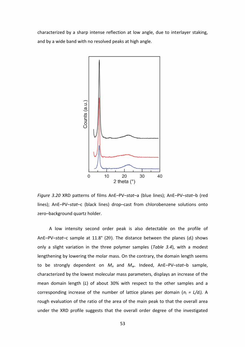
53
characterized by a sharp intense reflection at low angle, due to interlayer staking,
and by a wide band with no resolved peaks at high angle.
Figure 3.20 XRD patterns of films AnE–PV–stat–a (blue lines); AnE–PV–stat–b (red
lines); AnE–PV–stat–c (black lines) drop–cast from chlorobenzene solutions onto
zero–background quartz holder.
A low intensity second order peak is also detectable on the profile of
AnE–PV–stat–c sample at 11.8° (2). The distance between the planes (di) shows
only a slight variation in the three polymer samples (Table 3.4), with a modest
lengthening by lowering the molar mass. On the contrary, the domain length seems
to be strongly dependent on Mn and Mw. Indeed, AnE–PV–stat–b sample,
characterized by the lowest molecular mass parameters, displays an increase of the
mean domain length (L) of about 30% with respect to the other samples and a
corresponding increase of the number of lattice planes per domain (ni = L/di). A
rough evaluation of the ratio of the area of the main peak to that the overall area
under the XRD profile suggests that the overall order degree of the investigated
54
polymer films follows the order: AnE–PV–stat–c > AnE–PV–stat–b > AnE–PV–stat–a.
However, if the number of lattice planes per domain is considered, AnE–PV–stat–b
results in the sample with the largest ordered domains. The comparison of the XRD
patterns of samples AnE–PV–stat–c and AnE–PV–stat–a, roughly showing the same
peak in the GPC curves but different PDI, suggests that polydispersity plays an
important role in the organization of polymer chains.
Table 3.4. XRD parameters of the three AnE–PV–stat samples: interlayer distance, peak
width FWHM, mean domain length and mean number of interlayer lattice per domain.
Donors di
(nm)
FWHM
(°, 2)
L
(nm)
ni
AnE-PV-stat-a 1.52 0.86 10.3 6.8
AnE-PV-stat-b 1.53 0.67 13.2 8.6
AnE-PV-stat-a 1.50 0.84 10.5 7.0
The atomic force microscopy (AFM) inspection of films deposited in the same
conditions used for the XRD investigation revealed a close correlation between the
macromolecular parameters and the film topology (Figure 3.21). Polymer chains in
AnE–PV–stat–b film, with the lowest Mw, were able to pack in smaller domains,
compared with the samples with higher molar mass, while a prevailing fibril–like
formation was observed for samples AnE–PV–stat–a and AnE–PV–stat–c. The
smaller–domain morphology of AnE–PV–stat–b film was also accomplished by a
higher root–mean–square roughness (Rq), compared to the films made of the
polymers with higher molar weight. The values of Rq evaluated on a scan area of
0.5 m × 0.5 m were 0.71, 1.58 and 1.34 nm for AnE–PV–stat–a, AnE–PV–stat–b
and AnE–PV–stat–c, respectively, and maintained the same trend over a larger scan
area of 1.0 m × 1.0 m. By comparing AnE–PV–stat–c and AnE–PV–stat–a,
exhibiting a similar Mw, the lower Rq was observed for the one showing the lower
polydispersity, indicating that the distribution of molecular weights plays a role in
the film morphology.

55
(a)
(c)
(b)
Figure 3.21 Three–dimensional AFM topography images of drop–casted films made of:
AnE–PV–stat–a (a); AnE–PV–stat–b (b); AnE–PV–stat–c (c).
The comparison of Figure 3.21a and 3.21c shows the effect of the different
polydispersity index on the film morphology. Indeed, the higher PDI of
AnE–PV–stat–c seems to be beneficial for a more regular arrangement of polymer
chains, confirming the XRD data, and as previously suggested for
poly(3–alkylthiophenes).[81]

56
3.5.3 Effect on charge carrier mobility
TOF experiments were carried out in the same conditions described in
paragraph 3.2. The polymer layers were drop–casted from the same chlorobenzene
solutions used for the preparation of the XRD and AFM samples. The film thickness
was 3.6, 4.2, 7.8 m for AnE–PV–stat–a, AnE–PV–stat–b and AnE–PV–stat–c,
respectively.
The photocurrent transients for the three AnE–PV–stat samples are displayed
in a double–logarithmic representation in Figure 3.22 for a comparable electric field
of about 1×10⁵ V cm-1.
10-6
10-5
10-5
10-4
(b)
Photo
curr
ent
(a.u
.)
AnE-PV-stat-c
AnE-PV-stat-c
AnE-PV-stat-b
AnE-PV-stat-b
AnE-PV-stat-a
AnE-PV-stat-a
Time (s)
(a)
Photo
curr
ent
(a.u
.)
Time (s)
Figure 3.22 Log–log plots of photocurrent signals for holes (a) and electrons (b) for a
comparable electric field of about 1×10⁵ V cm-1.

57
The shape of TOF signals shown in Figure 3.22 is representative for transients
observed for different values of E and indicates a quite dispersive transport. The
resulting values for charge carrier mobility are shown as a function of the applied
field in Figure 3.23.
5x10⁴
105
10-4
2x10⁻⁴
4x10⁻⁴
6x10⁻⁴
5x10⁴
105
4x10⁻⁴
6x10⁻⁴
8x10⁻⁴
10-3
2x10⁻³
(a)
h (
cm
2 V
-1 s
-1)
E (V cm-1)
(b)
e (
cm
2 V
-1 s
-1)
E (V cm-1)
Figure 3.23 Hole (a) and electron (b) drift mobility as a function of the applied electric field:
AnE–PV–stat–a (blue triangles); AnE–PV–stat–b (red circles); AnE–PV–stat–c (black squares).
Lines are shown to guide the dye.
As far as the trend of with E is concerned, being the same for both positive
and negative carriers for each AnE–PV–stat sample, again the main difference was
observed between AnE–PV–stat–a and the other two polymer samples, both
showing a higher overall degree of order as observed with XRD. It has already been
58
reported in paragraph 3.2 that charge carrier mobility in AnE–PV–stat–a films shows
a Poole–Frenkel behaviour both for holes and electrons,[82] with an exponential
increase of with the square–root of E.
Differently, mobility in AnE–PV–stat–c and AnE–PV–stat–b films exhibits a
decreasing trend for low fields and reaches a minimum before starting increasing
with E. For both types of carriers, drift mobility shows a clear dependence on the
macromolecular parameters. At low fields (below 5×10⁴ V cm-1), the hole mobility
seems to be correlated to the mean domain length (Table 3.4), with more ordered
polymer samples showing higher mobility. However hole mobility in sample
AnE–PV–stat–a surpasses that in sample AnE–PV–stat–c as E is increased, because
of the strong field activation of the less ordered polymer also at moderate electric
fields.
3.5.4 Effect on the performance of BHJ solar cells
Bulk heterojunction solar cells were prepared with the three AnE–PV–stat
samples, as electron–donors and PCBM as acceptor. Since, for a given D/A pair, the
maximum photovoltaic performance of the related blends is determined by a critical
interplay between different factors, such as miscibility, deposition conditions, blend
thickness, donor to acceptor ratio, pre – and/or post–treatments,[83] the comparison
of different D/A pairs is not so straightforward. For this reason the aim of this work
was not the optimization of solar cell devices, but to establish how the photovoltaic
properties of AnE–PV–stat:PCBM blends were affected when an organization of the
donor phase close to that of drop–casted thick films investigated by TOF, XRD and
AFM was induced. To this end, efforts were made to use deposition and treatment
conditions able to induce such organization in spin–coated thin films, required for
lab–scale solar cell preparation. The AnE–PV–stat:PCBM active layers were
deposited by using a not too high D/A ratio (1:1 w/w), the same solvent
(chlorobenzene), the same solution concentration (17 g L-1), the same low rotation
speed of the spin–coater (500 rpm). After the deposition, the AnE–PV–stat:PCBM
films were solvent–vapour annealed for one hour, in order to foster the polymer
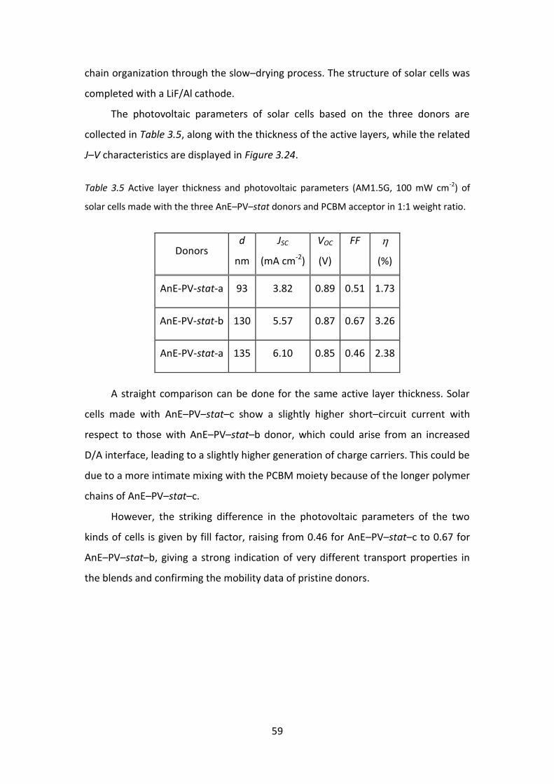
59
chain organization through the slow–drying process. The structure of solar cells was
completed with a LiF/Al cathode.
The photovoltaic parameters of solar cells based on the three donors are
collected in Table 3.5, along with the thickness of the active layers, while the related
J–V characteristics are displayed in Figure 3.24.
Table 3.5 Active layer thickness and photovoltaic parameters (AM1.5G, 100 mW cm-2) of
solar cells made with the three AnE–PV–stat donors and PCBM acceptor in 1:1 weight ratio.
Donors d
nm
JSC
(mA cm-2)
VOC
(V)
FF
(%)
AnE-PV-stat-a 93 3.82 0.89 0.51 1.73
AnE-PV-stat-b 130 5.57 0.87 0.67 3.26
AnE-PV-stat-a 135 6.10 0.85 0.46 2.38
A straight comparison can be done for the same active layer thickness. Solar
cells made with AnE–PV–stat–c show a slightly higher short–circuit current with
respect to those with AnE–PV–stat–b donor, which could arise from an increased
D/A interface, leading to a slightly higher generation of charge carriers. This could be
due to a more intimate mixing with the PCBM moiety because of the longer polymer
chains of AnE–PV–stat–c.
However, the striking difference in the photovoltaic parameters of the two
kinds of cells is given by fill factor, raising from 0.46 for AnE–PV–stat–c to 0.67 for
AnE–PV–stat–b, giving a strong indication of very different transport properties in
the blends and confirming the mobility data of pristine donors.
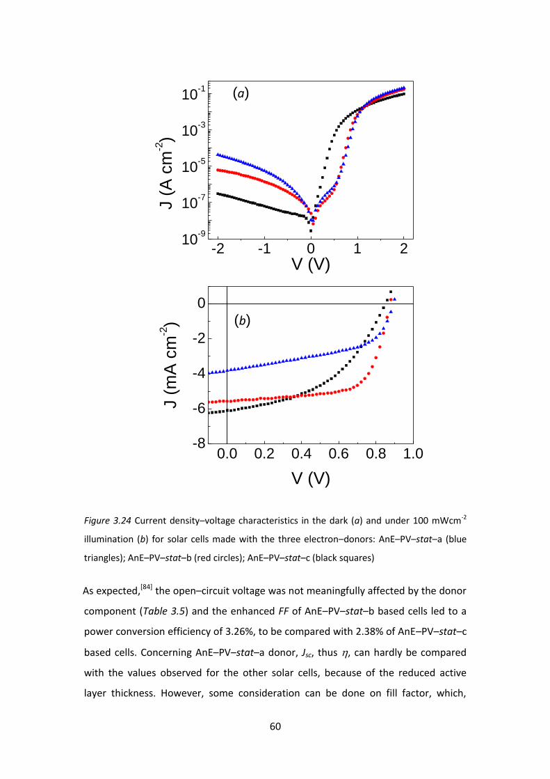
60
0.0 0.2 0.4 0.6 0.8 1.0-8
-6
-4
-2
0
-2 -1 0 1 210
-9
10-7
10-5
10-3
10-1
(b)
V (V)
J (
mA
cm
-2)
(a)
J (
A c
m-2)
V (V)
Figure 3.24 Current density–voltage characteristics in the dark (a) and under 100 mWcm-2
illumination (b) for solar cells made with the three electron–donors: AnE–PV–stat–a (blue
triangles); AnE–PV–stat–b (red circles); AnE–PV–stat–c (black squares)
As expected,[84] the open–circuit voltage was not meaningfully affected by the donor
component (Table 3.5) and the enhanced FF of AnE–PV–stat–b based cells led to a
power conversion efficiency of 3.26%, to be compared with 2.38% of AnE–PV–stat–c
based cells. Concerning AnE–PV–stat–a donor, Jsc, thus , can hardly be compared
with the values observed for the other solar cells, because of the reduced active
layer thickness. However, some consideration can be done on fill factor, which,

61
differently from Jsc, is not affected by the lower solar light harvesting ability of cells
made with AnE–PV–stat–a donor. Fill factor of AnE–PV–stat–a cells was found to be
0.51, in between those shown by the other cells, again confirming the trend of hole
mobility in pristine AnE–PV–stat films (Figure 3.23a). Figure 3.25 shows the straight
correlation between fill factor of solar cells and the mobility of positive carriers
measured in pristine AnE–PV–stat films at a field of about 1×10⁵ V cm-1.
AnE-PV-stat-a AnE-PV-stat-b AnE-PV-stat-c
0.5
0.6
0.7
1.5
2.0
2.5
3.0
h (
10
-4 c
m2 V
-1 s
-1)
FF
Figure 3.25 Fill factor of AnE–PV–stat:PCBM solar cells (left, blue circles) and TOF hole
mobility, at about 1×10⁵ V-1 cm-1, of pristine AnE–PV–stat films (right, red triangles)
3.6 Discussion
A systematic investigation of charge carrier mobility in films made of a series
of anthracene–containing poly (p–phenylene–ethynylene)–alt-poly(p–phenylene–
vinylene)s, bearing the same conjugated backbone, has been performed, in order to
establish the relationship between charge transport properties and (i) molecular
structure, (ii) macromolecular parameters, and (iii) deposition conditions for this
relevant class of conjugated polymers.
For the first time, we demonstrated the excellent ambipolar behaviour of this
class of conjugated polymers, which could be interesting for field–effect transistor
application. Indeed, AnE–PV polymers show a very good delocalization of HOMO
and LUMO levels, consistent with a good ability to transport both positive and
62
negative charge carriers. In addition, differently from other good ambipolar
conjugated polymers already reported in the literature, the bulk transport of
negative carriers is even faster than that of positive carriers, with a drift mobility of
fastest electrons of about six times higher than that evaluated for fastest holes in
the case of the best–performing AnE–PV investigated. These results suggest that
conjugated polymers with carbon–carbon triple bonds, rarely considered and
investigated, could represent a promising platform toward high performance
ambipolar materials for printable and plastic electronics.
For AnE–PV–stat we have also studied the effects of a slight variation of the
macromolecular parameters on its transport proprieties, as well as on the related
organic solar cells by using PCBM as electron–acceptor. Interestingly, a variation of
just a factor of around two in the molecular weight of AnE–PV–stat led to
appreciable modifications in the optical, morphological, and transport properties of
its films, reflecting in the behaviour of AnE–PV–stat:PCBM solar cells. Not only the
mobility data were affected by the macromolecular parameters, but also the trend
of with the applied electric field was found to be dependent on them. A
Poole–Frenkel–like behaviour was obtained for less ordered AnE–PV–stat–a films,
while a minimum of at around 1×10⁵ V-1 cm-1 was observed for the other two
polymer samples giving more ordered arrangements in cast–films. The comparison
of AnE–PV–stat–a and AnE–PV–stat–c, showing the same peak in the GPC curves but
different PDI, indicated that polydispersity plays a significant role in the organization
of polymer chains in the investigated films, thus affecting all their properties. In
addition, a strong correlation between the fill factor of AnE–PV–stat:PCBM solar
cells and the mobility of pristine AnE–PV–stat films was obtained, suggesting that
the tuning of the donor macromolecular parameters is critical for high performance
polymer/fullerene solar cells.
By changing the side–chains of AnE–PVs, relevant differences in charge
transport proprieties were observed for both positive and negative carriers. Indeed
the nature of the substituents has a great impact on charge carrier mobility of the
investigated polymers, with a variation observed of 2–3 orders of magnitude. Long
octyl and dodecyl linear chains have a detrimental effect on , likely because of a
less compact molecular packing, resulting in a decreased interaction between
63
adjacent hopping sites. Similarly, short methyl substituents induce low mobility
values, but because of a highly disordered arrangement of polymer chains in the
solid phase, also leading to an increased charge trapping. Indeed, a decreasing
mobility with the amount of methyl chains in the molecular structure was clearly
observed. Finally, the used experimental conditions, allowing for a straight
comparison of the investigated films, definitely confirmed the better properties of
random polymers, compared to the counterpart based on well–defined side–chain.
64
CHAPTER 4 – CHARGE TRANSPORT IN SOLAR CELLS
MADE OF BAND GAP CONJUGATED POLYMERS AND
NEAT-C70
In this chapter, the effects of charge transport in BHJ solar cells, made of
blends between low band gap conjugated polymers (electron–donors) and
neat–fullerenes (electron–acceptors), are investigated.
Low cost, both of active materials and processing techniques for module
production, is one of the main advantages of this innovative photovoltaic
technology: the aim of this work, carried out within an industrial research project on
organic solar cell, is to give a contribution to further restrain the costs of materials.
The approach of this thesis is the replacement of the common soluble derivatives of
fullerene with neat fullerenes (C60 and C70), much less soluble[85] but with a cost
one–tenth that of functionalized fullerenes. C70 was preferred to C60, because of its
moderate absorption in the visible range.[86]
The use of a third component, a pyrene derivative, was also considered for a
better dispersion of the poorly soluble C70 in the polymer matrix.
4.1. Materials
A copolymer based on poly(2,7–carbazole) derivatives, poly(N–9’’–hepta–
decanyl–2,7–carbazole–alt–5,5– (4’,7’–di–2–thienyl–2’,1’,3’–benzothiadiazole)
(PCDTBT) and a copolymer made of thiophene and benzodithiophene,
thieno[3,4–b]–thiophene/benzodithiophene (PTB7, Luminescence Technology Corp.)
were used as electron–donors.
In addition to solar cells made of neat–C70, reference devices were prepared
with [6,6]–phenyl C71–butyric acid methyl ester (PC70BM) as acceptor. Both
electron–acceptors were purchased by Sigma–Aldrich.
In order to obtain a better dispersion of C70, a third component, butyl
1–pyrenebutyrate (PyBB) was introduced in the blends.

65
PCDTBT and PyBB were synthesized at the Research Center for non
Conventional Energies, Istituto ENI Donegani, ENI S.p.A. PCDTBT was synthesized
according to a previously reported method[87] while PyBB was prepared through a
simple reaction of esterification with 1–butanol, starting from the commercial
1–pyrenebutyric acid in the presence of catalytic amount of H2SO4. All materials
were used as received. Figure 4.1 shows the molecular structure and the energy
levels of the materials used in this chapter.
-2
-4
-6
Energ
y (
eV
)
- 5.15
- 3.31
- 3.90
- 6.00
- 4.60
- 6.80
- 5.50
- 3.60
PC
DT
BT
Vacuum
PT
B7
PC
70B
M
C70
PyB
B
- 2.36
- 5.57
Figure 4.1 Molecular structure and energy levels of the materials used in this chapter.
CO2CH3
O
O
PCDTBT PBT7
C70 PC70BM PyBB

66
4.2 Solar cells made of neat–C70 as electron acceptor
Solar cells with PC70BM as electron–acceptor were first prepared with both
conjugated polymers, according to optimized procedures already reported in the
literature for the active layer deposition and composition.[88, 89] In particular,
PTB7:PC70BM solar cells were prepared in 1:1.5 weight ratio and deposited from a
chlorobenzene solution (25 g L-1) with 1,8–diiodooctane (3% vol) as additive, while
PCDTBT:PC70BM (1:4 w/w) devices were spin–coated from 1,2–dichlorobenzene
(17.5 g L-1). C70–based solar cells were prepared in different D/A ratios from
1,2–dichlorobenzene solutions: PTB7:C70 (1:2 w/w, 28 g L-1) devices were deposited
at 900 rpm while PCDTBT:C70 (1:1 w/w, 10 g L-1; 1:2 w/w, 11 g L-1; 1:3 w/w, 12 g L-1
and 1:4 w/w, 17.5 g L-1) at 1000 rpm. For a better comparison of the cells made of
the same donor, PTB7–based cells and PCDTBT–based ones, were prepared with the
same thickness of the active layer, 100 nm and 70 nm respectively. Then the
samples were transferred to the glove–box where the device structure was
completed with the thermal evaporation of the top electrode Al (100nm).
The use of additives (1,8–diiodooctane, 1–chloronaphtalene,
1–methyl–2–pyrrolidinone) or thermal treatments were not effective in improving
the performance of devices made of C70.
4.2.1 Photovoltaic parameters
The J–V characteristics in the dark and under 100 mW cm-2 (AM1.5G)
illumination of as–cast PTB7:C70 and PCDTBT:C70 solar cells are shown in Figure 4.2
and Figure 4.3, respectively, and compared with those obtained for the reference
cells with PC70BM, while the extracted photovoltaic parameters are collected in
Table 4.1.
67
-2 -1 0 1 2
10-4
10-2
100
102
(a)
J (
mA
cm
-2)
V (V)
0.0 0.2 0.4 0.6 0.8 1.0
-15
-10
-5
0
5
(b)
J (
mA
cm
-2)
V (V)
Figure 4.2 Current density – voltage characteristics in the dark (a) and under 100 mW cm-2
illumination (b) of solar cells made of PTB7:PC70BM (black squares), PTB7:C70 (1:2 w/w) (red
circles) and PTB7:C70 (1:3 w/w) (blue triangles).
68
-2 -1 0 1 2
10-3
10-1
101
103 (a)
J (
mA
cm
-2)
V (V)
0.0 0.2 0.4 0.6 0.8 1.0
-15
-10
-5
0
5
(b)
J (
mA
cm
-2)
V (V)
Figure 4.3 Current density – voltage characteristics in the dark (a) and under 100 mW cm-2
illumination (b) of solar cells made of PCDTBT:PC70BM (black squares), PCDTBT:C70
(1:1 w/w) (red circles), PCDTBT:C70 (1:2 w/w) (blue up triangles), PTB7:C70 (1:3 w/w) (cyan
down triangles) and PTB7:C70 (1:4 w/w) (dark yellow diamonds)
69
Table 4.1 Photovoltaic parameters at 100 mW cm-2 (AM1.5G).
Active layer D:A
(w/w)
JSC
(mA cm-2)
VOC
(V)
FF
(%)
PTB7:PC70BM 1:1.5 13.34 0.71 0.59 5.73
PTB7:C70 1:2 9.21 0.59 0.41 2.22
PTB7:C70 1:3 9.08 0.61 0.55 3.17
PCDTBT:PC70BM 1:4 8.41 0.91 0.62 4.80
PCDTBT:C70 1:1 8.50 0.67 0.40 2.30
PCDTBT:C70 1:2 11.31 0.78 0.50 4.44
PCDTBT:C70 1:3 13.81 0.77 0.43 4.55
PCDTBT:C70 1:4 10.15 0.74 0.53 4.02
The values calculated for the power conversion efficiency of the reference
cells were comparable to those reported in previous studies,[88,89] with of 5.73%
calculated for PTB7:PC70BM devices and of 4.80% for PCDTBT:PC70BM cells. As
shown in Table 4.1, the replacement of PC70BM with C70 led to the decrease of all
photovoltaic parameters, with the only exception of the short–circuit current
density of PCDTBT:C70 solar cells. Indeed, differently from PTBT:C70 devices, for
which a significant reduction of Jsc was observed (Jsc of 9.08 and 9.21 mA cm-2 for the
two D/A ratios) compared to the related reference cell (13.34 mA cm-2), the change
of the polymer donor resulted in an enhanced short–circuit current for neat–C70
devices, with a Jsc ranging between 8.50 and 13.81 mA cm-2, to be compared with
8.41 mA cm-2 measured for PCDTBT:PC70BM solar cells. The different behaviour of Jsc
could be related to a different charge generation ability of the blends made of the
two polymers, due to a different distribution of the D/A interface. In addition, the
higher molar extinction coefficient of C70, compared to PC70BM, could be the origin

70
of the enhanced Jsc observed for PCDTBT:C70 solar cells with respect to the
PCDTBT:PC70BM ones, as shown in Figure 4.4.
300 400 500 600 700 8000.0
0.1
0.2
0.3
PCDTBT : PC70
BM (1:4 w/w)
PCDTBT : C70
(1:4 w/w)
Extinction c
oeffic
ient
(nm)
Figure 4.4 Extinction coefficients of PCDTBT:PC70BM (black line) and of PCDTBT:C70 (red line)
blends, prepared with the same D/A weight ratio of 1:4.
The open–circuit voltage decreased from 0.71 V and 0.62 V of the reference
cells made of PTB7 and PCDTBT, respectively, to values of around 0.6 V for PTB7:C70
cells and ranging between 0.67 and 0.78 V in the case of PCDTBT donor. The
reduction of Voc upon replacing PC70BM with C70 could be explained by the effect of
the higher leakage currents observed for cells made of neat–C70 (Figure 4.2a and
4.3a) as well as by the different electron affinities of the electron-acceptors.[90] Also
fill factor was found to decrease for all C70–based solar cells, irrespective of the
donor and of the D/A ratio, indicating higher losses for charge recombination,
though FF is also affected by leakage paths. FF values in the range 0.41–0.55 were
achieved for PTB7:C70 solar cells and between 0.40 and 0.53 for PCDTBT:C70 devices,
against 0.59 and 0.62 calculated for the respective reference cells. Nevertheless,
despite the loss of efficiency of solar cells made with C70, good performances were
obtained with PCDTBT donor at high fullerene contents. PCDTBT:C70 cells prepared
with 1:3 D/A ratio showed a Jsc of 13.81 mA cm-2, Voc = 0.77 V and FF of 43%,
resulting in an efficiency of 4.55%, reduced by about 5% with respect to 4.80%

71
calculated for PCDCTBT:PC70BM reference cell. On the contrary, for the best
PTBT:C70 solar cells (1:3 weght ratio) a reduction of of about 45% was observed by
replacing PC70BM with neat–C70.
4.2.2 Analysis of photocurrents
In order to investigate the loss mechanisms in cells made of neat–C70, the
behaviour of photocurrents was analyzed as a function of voltage at different values
of the light power intensity, and compared with that observed for the reference
cells. The trend of the net photocurrent, is plotted in Figure 4.5 and 4.6 versus the
effective voltage for PTB7 and PCDTBT–based solar cells, respectively.
Figure 4.5 Net photocurrent as a function of the effective voltage at different light power
intensities (8–100 mW cm-2) for PTB7:PC70BM (1:1.5 w/w) (a) and PTB7:C70 (1:3 w/w) (b)
solar cells. Short–circuit (SC) and maximum power point (MPP) conditions are indicated by
the arrows for the curves obtained at 100 mW cm-2.
0.1 1 10
10-3
10-2
MPP SC
(a)
Pin
Jph (
A c
m-2)
V0-V (V)
0.1 110
-4
10-3
10-2
(b)
MPP SC
Pin
Jph (
A c
m-2)
V0-V (V)

72
Figure 4.6 Net photocurrent as a function of the effective voltage at different light power
intensities (8–100 mW cm-2) for PCDTBT:PC70BM (1:4 w/w) (a) and PCDTBT:C70 (1:3 w/w) (b)
solar cells. Short–circuit (SC) and maximum power point (MPP) conditions are indicated by
the arrows for the curves obtained at 100 mW cm-2.
For PTB7:PC70BM solar cells, Jph quickly saturates, showing a nearly constant
value with the effective voltage. In these devices, charge carriers are efficiently
collected at the electrodes with no recombination losses, even at low effective
voltages, relevant for solar cell operation. Differently, a voltage–dependent
behaviour of Jph was observed for PCDCTB:PC70BM solar cells (Figure 4.6a), with the
saturation reached at an effective voltage of around 0.3 V independently of Pin and
with a linear trend of Jph with Pin at low V0-V. It is worth noting that in all cases Jph is
not significantly limited at short–circuit conditions, indicating that the built–in
voltage is enough to sweep charge carriers out of the cells before they recombine.
Differently, at lower fields, as at the maximum power point, recombination losses
were observed for all cells made of neat–C70 as well as for PCDTBT–based reference
cells, reflecting in the lower values of FF compared to the recombination–free
PTBT:PC70BM devices (Table 4.1).
The different behaviour of Jph in the range of low effective voltage could be
attributed to different charge transport properties in the blends made of the two
different donors. The mobility of charge carriers in PTBT:PC70BM blend should be
high enough to allow the extraction of charges before recombination even at very
0.1 1 10
10-4
10-3
10-2
10-1
MPPSC
(a)
Pin
J
ph (
A c
m-2)
V0-V (V)
0.1 1 10
10-3
10-2
(b)SC
MPP
Jph (
A c
m-2)
V0-V (V)
73
low effective voltages, while a lower mobility in PCDTBT:PC70BM solar cells could
account for the field–dependent Jph observed at low V0–V, indicating that the drift
length of charge carriers, the path they can cover before recombination, is lower
than the blend thickness at those effective voltages and leading to a recombination
loss.[91] In effect, the mobility of holes in the donor phase is expected to be higher in
PTB7 than in PCDTBT,[92] though charge carrier mobility is extremely dependent on
the D/A ratio and the deposition conditions of the blends.
A square–root dependence of Jph with V0–V was not observed for
PCDTBT:PC70BM solar cells in any range of the effective voltage, excluding for these
cells space–charge effects or limitation of the photocurrent due to a low
product.[93, 94] On the contrary, a square–root regime before saturation was
observed for all cells made with neat–C70, as shown in Figure 4.5b and 4.6b for
PTB7:C70 (1:3 w/w) and PCDTBT:C70 (1:3 w/w), respectively. To discern between the
two possible limiting processes originating this behavior, space–charge formation or
low , the trend of Jph and that of the saturation voltage was analyzed with Pin. The
results obtained for PTB7:C70 (1:3 w/w) solar cells are shown in Figure 4.7 in
bilogarithmic plots. The slope of Jph vs Pin, both at high (SHV) and at low effective
voltage (SLV) is close to 1. 0.95 and 0.91 were calculated, respectively for SHV and SLV,
for PTB7:C70 solar cells prepared in 1:3 weight ratio. The ¾ power dependence of the
photocurrent on the incident light was not observed at low Pin, indicating that Jph is
not limited by the occurrence of space–charge in these cells. The confirmation came
from the behavior of Vsat, appearing nearly independent of Pin,[95] so showing a slope
with Pin (Ssat) close to zero (a value of 0.09 was obtained for Ssat in PTB7:C70 solar
cells 1:3 w/w).
The same behaviour with light intensity was achieved for the other cells made
with neat–C70, as indicated by the values of SHV, SLV and Ssat collected in Table 4.2.
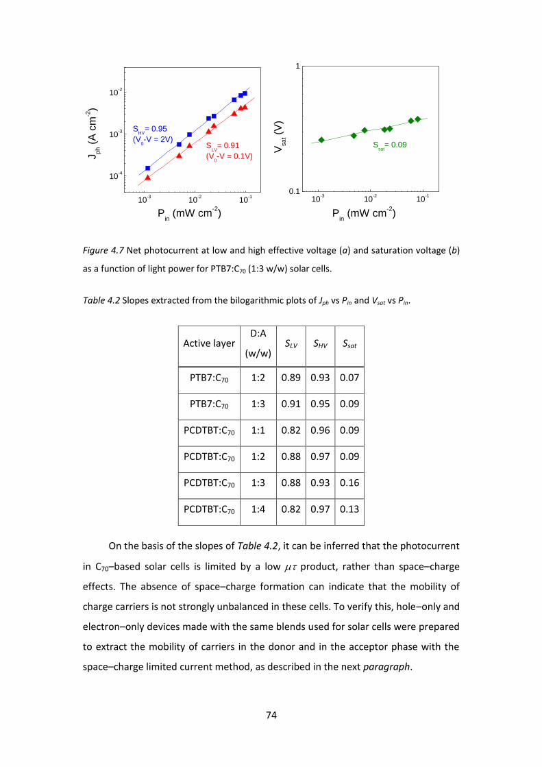
74
Figure 4.7 Net photocurrent at low and high effective voltage (a) and saturation voltage (b)
as a function of light power for PTB7:C70 (1:3 w/w) solar cells.
Table 4.2 Slopes extracted from the bilogarithmic plots of Jph vs Pin and Vsat vs Pin.
Active layer D:A
(w/w) SLV SHV Ssat
PTB7:C70 1:2 0.89 0.93 0.07
PTB7:C70 1:3 0.91 0.95 0.09
PCDTBT:C70 1:1 0.82 0.96 0.09
PCDTBT:C70 1:2 0.88 0.97 0.09
PCDTBT:C70 1:3 0.88 0.93 0.16
PCDTBT:C70 1:4 0.82 0.97 0.13
On the basis of the slopes of Table 4.2, it can be inferred that the photocurrent
in C70–based solar cells is limited by a low product, rather than space–charge
effects. The absence of space–charge formation can indicate that the mobility of
charge carriers is not strongly unbalanced in these cells. To verify this, hole–only and
electron–only devices made with the same blends used for solar cells were prepared
to extract the mobility of carriers in the donor and in the acceptor phase with the
space–charge limited current method, as described in the next paragraph.
10-3
10-2
10-1
10-4
10-3
10-2
SHV
= 0.95
(V0-V = 2V)
SLV
= 0.91
(V0-V = 0.1V)J
ph (
A c
m-2)
Pin (mW cm
-2)
10-3
10-2
10-1
0.1
1
Ssat
= 0.09
Vsat (
V)
Pin (mW cm
-2)
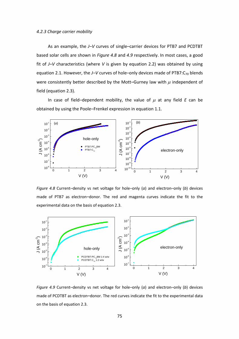
75
4.2.3 Charge carrier mobility
As an example, the J–V curves of single–carrier devices for PTB7 and PCDTBT
based solar cells are shown in Figure 4.8 and 4.9 respectively. In most cases, a good
fit of J–V characteristics (where V is given by equation 2.2) was obtained by using
equation 2.1. However, the J–V curves of hole–only devices made of PTB7:C70 blends
were consistently better described by the Mott–Gurney law with independent of
field (equation 2.3).
In case of field–dependent mobility, the value of at any field E can be
obtained by using the Poole–Frenkel expression in equation 1.1.
Figure 4.8 Current–density vs net voltage for hole–only (a) and electron–only (b) devices
made of PTB7 as electron–donor. The red and magenta curves indicate the fit to the
experimental data on the basis of equation 2.3.
Figure 4.9 Current–density vs net voltage for hole–only (a) and electron–only (b) devices
made of PCDTBT as electron–donor. The red curves indicate the fit to the experimental data
on the basis of equation 2.3.
0 1 2 3 410
-10
10-9
10-8
10-7
10-6
10-5
10-4
10-3
10-2
10-1 (b)
electron-only
J (
A c
m-2)
V (V)
0 1 2 3 410
-7
10-6
10-5
10-4
10-3
10-2
10-1
electron-only
J (
A c
m2)
V (V)
0 1 2 3 410
-8
10-7
10-6
10-5
10-4
10-3
10-2
10-1 (a)
hole-only
PTB7:PC70
BM
PTB7:C70
J (
A c
m-2)
V (V)
0 1 2 3 410
-7
10-6
10-5
10-4
10-3
10-2
10-1
hole-only
J (
A c
m-2)
V (V)
PCDTBT:PC70
BM 1:4 w/w
PCDTBT:C70
1:2 w/w

76
The series resistance was previously determined in devices with the same
geometry and contacts of the single–carrier ones, but without the polymer/fullerene
blend. The values of mobility calculated for a field of 5×10⁴ V cm-1, corresponding to
a potential of 0.5 V across a film 100 nm thick and close to the net potential at the
maximum power point of the cells, are summarized in Table 4.3.
Table 4.3 Charge carrier mobility extracted from the J–V curves of single–carrier devices.
The mobility values are calculated for an electric field of 5×10⁴ V cm-1.
Active layer D:A
(w/w)
h
(cm2 V-1 s-1)
e
(cm2 V-1 s-1)
PTB7:PC70BM 1:1.5 3.79 × 10⁻⁴ 4.56 × 10⁻⁴
PTB7:C70 1:2 7.29 × 10⁻⁵ 1.97 × 10⁻⁴
PTB7:C70 1:3 7.02 × 10⁻⁵ 4.25 × 10⁻⁴
PCDTBT:PC70BM 1:4 4.48 × 10⁻⁵ 3.06 × 10⁻⁵
PCDTBT:C70 1:2 3.66 × 10⁻⁶ 1.37 × 10⁻⁵
PCDTBT:C70 1:3 2.77 × 10⁻⁶ 1.15 × 10⁻⁵
PCDTBT:C70 1:4 3.17 × 10⁻⁶ 3.20 × 10⁻⁵
The mobility data of Table 4.3 indicate a perfectly balanced charge transport
for the reference solar cells, with mobilities in agreement with those already
reported for the same blends prepared in similar conditions[96] and with the
expected higher values for PTB7:PC70BM cells. Upon replacing PC70BM with C70,
significant variations of the mobility of negative carriers were not observed, whereas
a systematic decrease of the mobility of holes was obtained for both donors. The
mobility of positive carriers was reduced by about 5 folds in PTB7:C70 blends and by
roughly one order of magnitude in PCDTBT:C70 ones, resulting in charge carrier
mobilities not strongly unbalanced, consistent with the absence of space–charge
formation in the C70–based solar cells.
The reduction of mobility in blends made of neat C70, compared to the
reference ones prepared with PC70BM as acceptor, could explain the photocurrents
limited by a low product.
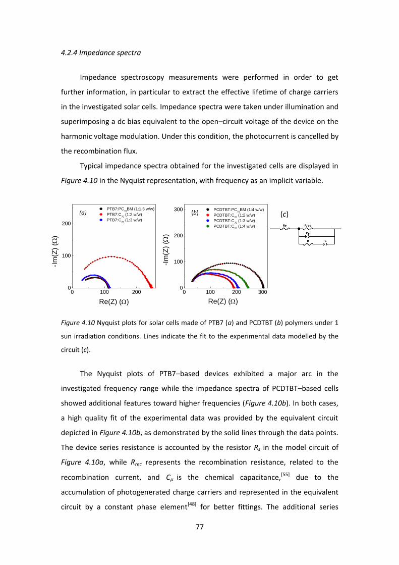
77
4.2.4 Impedance spectra
Impedance spectroscopy measurements were performed in order to get
further information, in particular to extract the effective lifetime of charge carriers
in the investigated solar cells. Impedance spectra were taken under illumination and
superimposing a dc bias equivalent to the open–circuit voltage of the device on the
harmonic voltage modulation. Under this condition, the photocurrent is cancelled by
the recombination flux.
Typical impedance spectra obtained for the investigated cells are displayed in
Figure 4.10 in the Nyquist representation, with frequency as an implicit variable.
Figure 4.10 Nyquist plots for solar cells made of PTB7 (a) and PCDTBT (b) polymers under 1
sun irradiation conditions. Lines indicate the fit to the experimental data modelled by the
circuit (c).
The Nyquist plots of PTB7–based devices exhibited a major arc in the
investigated frequency range while the impedance spectra of PCDTBT–based cells
showed additional features toward higher frequencies (Figure 4.10b). In both cases,
a high quality fit of the experimental data was provided by the equivalent circuit
depicted in Figure 4.10b, as demonstrated by the solid lines through the data points.
The device series resistance is accounted by the resistor Rs in the model circuit of
Figure 4.10a, while Rrec represents the recombination resistance, related to the
recombination current, and Cis the chemical capacitance,[55] due to the
accumulation of photogenerated charge carriers and represented in the equivalent
circuit by a constant phase element[48] for better fittings. The additional series
0 100 200 3000
100
200
300(b)
PCDTBT:PC70
BM (1:4 w/w)
PCDTBT:C70
(1:2 w/w)
PCDTBT:C70
(1:3 w/w)
PCDTBT:C70
(1:4 w/w)
-Im
(Z)
()
Re(Z) ()
0 100 2000
100
200
(a) PTB7:PC
70BM (1:1.5 w/w)
PTB7:C70
(1:2 w/w)
PTB7:C70
(1:3 w/w)
-Im
(Z)
()
Re(Z) ()
(c)
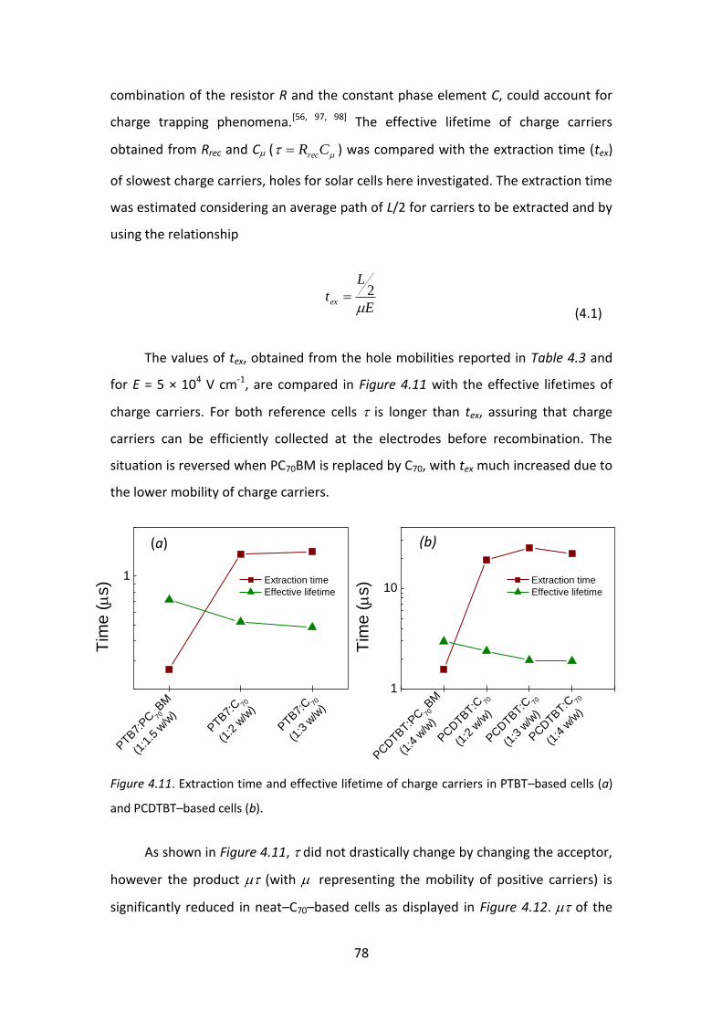
78
combination of the resistor R and the constant phase element C, could account for
charge trapping phenomena.[56, 97, 98] The effective lifetime of charge carriers
obtained from Rrec and C( CRrec ) was compared with the extraction time (tex)
of slowest charge carriers, holes for solar cells here investigated. The extraction time
was estimated considering an average path of L/2 for carriers to be extracted and by
using the relationship
E
L
tex
2
(4.1)
The values of tex, obtained from the hole mobilities reported in Table 4.3 and
for E = 5 × 10⁴ V cm-1, are compared in Figure 4.11 with the effective lifetimes of
charge carriers. For both reference cells is longer than tex, assuring that charge
carriers can be efficiently collected at the electrodes before recombination. The
situation is reversed when PC70BM is replaced by C70, with tex much increased due to
the lower mobility of charge carriers.
Figure 4.11. Extraction time and effective lifetime of charge carriers in PTBT–based cells (a)
and PCDTBT–based cells (b).
As shown in Figure 4.11, did not drastically change by changing the acceptor,
however the product (with representing the mobility of positive carriers) is
significantly reduced in neat–C70–based cells as displayed in Figure 4.12. of the
1
10
(b)
PCDTB
T:C 70
(1:4
w/w
)
PCDTB
T:C 70
(1:3
w/w
)
PCDTB
T:PC 70
BM
(1:4
w/w
)
PCDTB
T:C 70
(1:2
w/w
)
Tim
e (
s) Extraction time
Effective lifetime
1
(a)
PTB
7:PC 70
BM
(1:1
.5 w
/w)
PTB
7:C 70
(1:3
w/w
)
PTB
7:C 70
(1:2
w/w
)
Tim
e (
s) Extraction time
Effective lifetime
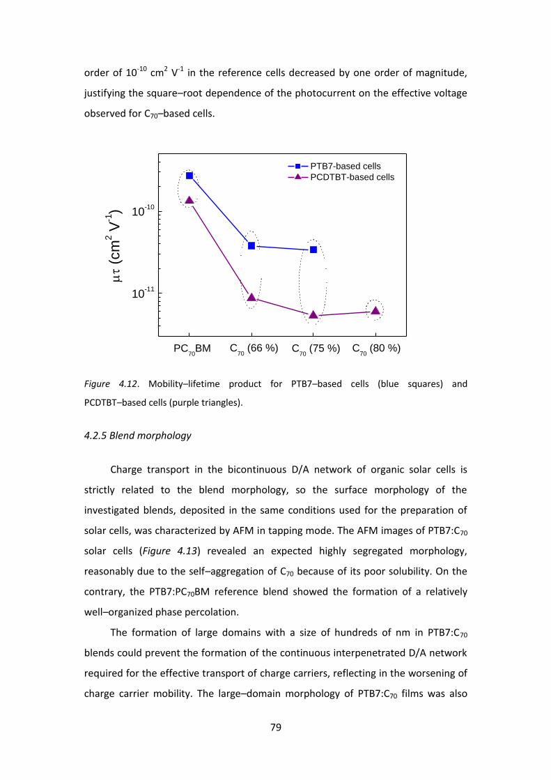
79
order of 10-10 cm2 V-1 in the reference cells decreased by one order of magnitude,
justifying the square–root dependence of the photocurrent on the effective voltage
observed for C70–based cells.
Figure 4.12. Mobility–lifetime product for PTB7–based cells (blue squares) and
PCDTBT–based cells (purple triangles).
4.2.5 Blend morphology
Charge transport in the bicontinuous D/A network of organic solar cells is
strictly related to the blend morphology, so the surface morphology of the
investigated blends, deposited in the same conditions used for the preparation of
solar cells, was characterized by AFM in tapping mode. The AFM images of PTB7:C70
solar cells (Figure 4.13) revealed an expected highly segregated morphology,
reasonably due to the self–aggregation of C70 because of its poor solubility. On the
contrary, the PTB7:PC70BM reference blend showed the formation of a relatively
well–organized phase percolation.
The formation of large domains with a size of hundreds of nm in PTB7:C70
blends could prevent the formation of the continuous interpenetrated D/A network
required for the effective transport of charge carriers, reflecting in the worsening of
charge carrier mobility. The large–domain morphology of PTB7:C70 films was also
10-11
10-10
C70
(80 %)C70
(75 %)C70
(66 %)PC70
BM
(cm
2 V
-1)
PTB7-based cells
PCDTBT-based cells
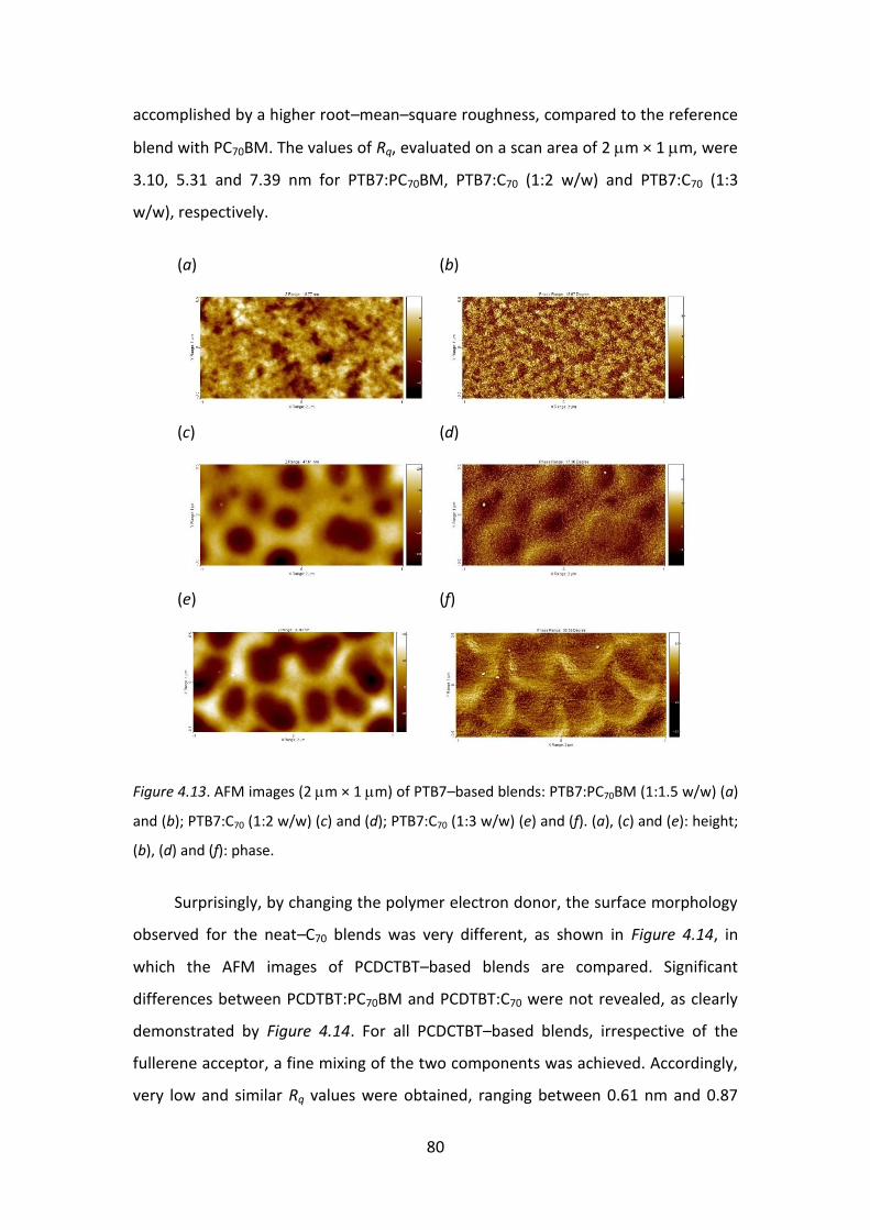
80
accomplished by a higher root–mean–square roughness, compared to the reference
blend with PC70BM. The values of Rq, evaluated on a scan area of 2 m × 1 m, were
3.10, 5.31 and 7.39 nm for PTB7:PC70BM, PTB7:C70 (1:2 w/w) and PTB7:C70 (1:3
w/w), respectively.
(a)
(b)
(c)
(d)
(e)
(f)
Figure 4.13. AFM images (2 m × 1 m) of PTB7–based blends: PTB7:PC70BM (1:1.5 w/w) (a)
and (b); PTB7:C70 (1:2 w/w) (c) and (d); PTB7:C70 (1:3 w/w) (e) and (f). (a), (c) and (e): height;
(b), (d) and (f): phase.
Surprisingly, by changing the polymer electron donor, the surface morphology
observed for the neat–C70 blends was very different, as shown in Figure 4.14, in
which the AFM images of PCDCTBT–based blends are compared. Significant
differences between PCDTBT:PC70BM and PCDTBT:C70 were not revealed, as clearly
demonstrated by Figure 4.14. For all PCDCTBT–based blends, irrespective of the
fullerene acceptor, a fine mixing of the two components was achieved. Accordingly,
very low and similar Rq values were obtained, ranging between 0.61 nm and 0.87

81
nm. The images of Figure 4.14 indicate that, differently from PTB7, PCDTBT acts as
an excellent dispersing medium for C70 molecules, enabling low–cost and efficient
neat–C70 solar cells.
(a)
(b)
(c)
(d)
(e)
(f)
(g)
(h)
Figure 4.14. AFM images (2 m × 1 m) of PCDTBT–based blends: PCDTBT:PC70BM (1:4
w/w) (a) and (b); PCDTBT:C70 (1:1 w/w) (c) and (d); PCDTBT:C70 (1:2 w/w) (e) and (f);
PCDTBT:C70 (1:4 w/w)(g) and (h). (a), (c), (e) and (g): height; (b), (d), (f) and (h): phase.
The morphology of the blends is an agreement with the values of the
short–circuit current reported in Table 4.1. Indeed, the reduction of Jsc in
PTB7–based solar cells by replacing PC70BM with C70 can be clearly attributed to the
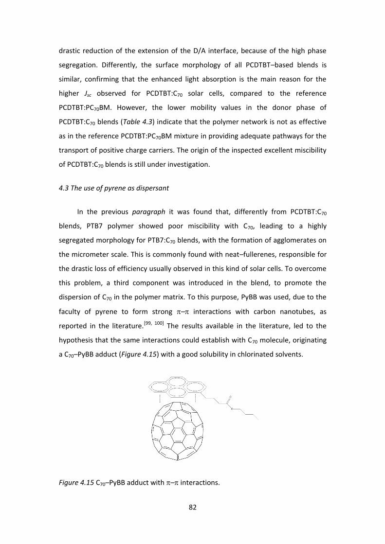
82
drastic reduction of the extension of the D/A interface, because of the high phase
segregation. Differently, the surface morphology of all PCDTBT–based blends is
similar, confirming that the enhanced light absorption is the main reason for the
higher Jsc observed for PCDTBT:C70 solar cells, compared to the reference
PCDTBT:PC70BM. However, the lower mobility values in the donor phase of
PCDTBT:C70 blends (Table 4.3) indicate that the polymer network is not as effective
as in the reference PCDTBT:PC70BM mixture in providing adequate pathways for the
transport of positive charge carriers. The origin of the inspected excellent miscibility
of PCDTBT:C70 blends is still under investigation.
4.3 The use of pyrene as dispersant
In the previous paragraph it was found that, differently from PCDTBT:C70
blends, PTB7 polymer showed poor miscibility with C70, leading to a highly
segregated morphology for PTB7:C70 blends, with the formation of agglomerates on
the micrometer scale. This is commonly found with neat–fullerenes, responsible for
the drastic loss of efficiency usually observed in this kind of solar cells. To overcome
this problem, a third component was introduced in the blend, to promote the
dispersion of C70 in the polymer matrix. To this purpose, PyBB was used, due to the
faculty of pyrene to form strong – interactions with carbon nanotubes, as
reported in the literature.[99, 100] The results available in the literature, led to the
hypothesis that the same interactions could establish with C70 molecule, originating
a C70–PyBB adduct (Figure 4.15) with a good solubility in chlorinated solvents.
Figure 4.15 C70–PyBB adduct with – interactions.
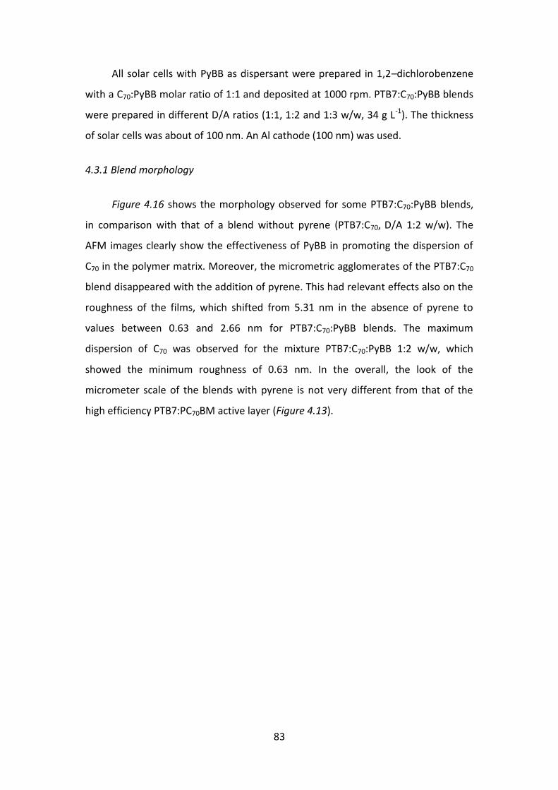
83
All solar cells with PyBB as dispersant were prepared in 1,2–dichlorobenzene
with a C70:PyBB molar ratio of 1:1 and deposited at 1000 rpm. PTB7:C70:PyBB blends
were prepared in different D/A ratios (1:1, 1:2 and 1:3 w/w, 34 g L-1). The thickness
of solar cells was about of 100 nm. An Al cathode (100 nm) was used.
4.3.1 Blend morphology
Figure 4.16 shows the morphology observed for some PTB7:C70:PyBB blends,
in comparison with that of a blend without pyrene (PTB7:C70, D/A 1:2 w/w). The
AFM images clearly show the effectiveness of PyBB in promoting the dispersion of
C70 in the polymer matrix. Moreover, the micrometric agglomerates of the PTB7:C70
blend disappeared with the addition of pyrene. This had relevant effects also on the
roughness of the films, which shifted from 5.31 nm in the absence of pyrene to
values between 0.63 and 2.66 nm for PTB7:C70:PyBB blends. The maximum
dispersion of C70 was observed for the mixture PTB7:C70:PyBB 1:2 w/w, which
showed the minimum roughness of 0.63 nm. In the overall, the look of the
micrometer scale of the blends with pyrene is not very different from that of the
high efficiency PTB7:PC70BM active layer (Figure 4.13).
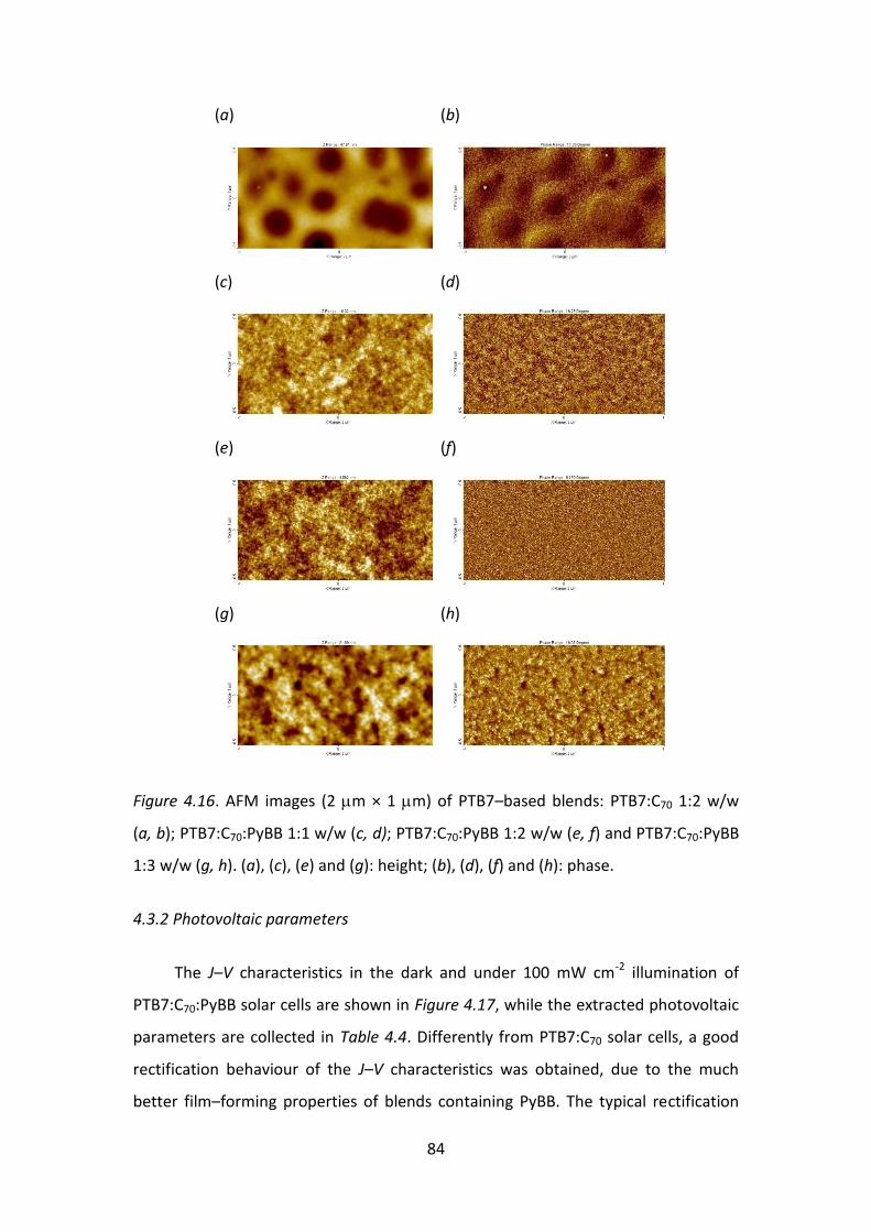
84
(a)
(b)
(c)
(d)
(e)
(f)
(g)
(h)
Figure 4.16. AFM images (2 m × 1 m) of PTB7–based blends: PTB7:C70 1:2 w/w
(a, b); PTB7:C70:PyBB 1:1 w/w (c, d); PTB7:C70:PyBB 1:2 w/w (e, f) and PTB7:C70:PyBB
1:3 w/w (g, h). (a), (c), (e) and (g): height; (b), (d), (f) and (h): phase.
4.3.2 Photovoltaic parameters
The J–V characteristics in the dark and under 100 mW cm-2 illumination of
PTB7:C70:PyBB solar cells are shown in Figure 4.17, while the extracted photovoltaic
parameters are collected in Table 4.4. Differently from PTB7:C70 solar cells, a good
rectification behaviour of the J–V characteristics was obtained, due to the much
better film–forming properties of blends containing PyBB. The typical rectification
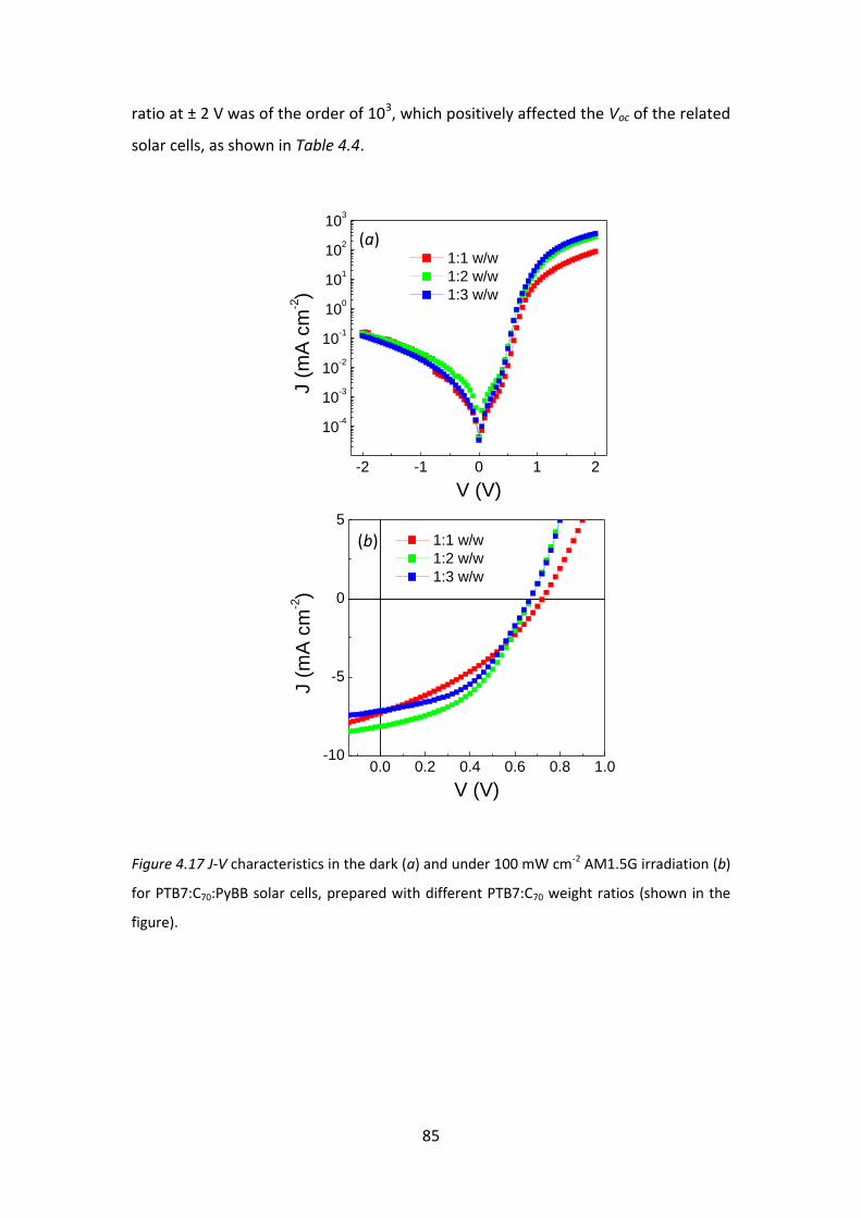
85
ratio at ± 2 V was of the order of 103, which positively affected the Voc of the related
solar cells, as shown in Table 4.4.
-2 -1 0 1 2
10-4
10-3
10-2
10-1
100
101
102
103
0.0 0.2 0.4 0.6 0.8 1.0-10
-5
0
5
1:1 w/w
1:2 w/w
1:3 w/w
(a)
J (
mA
cm
-2)
V (V)
1:1 w/w
1:2 w/w
1:3 w/w
(b)
J (
mA
cm
-2)
V (V)
Figure 4.17 J-V characteristics in the dark (a) and under 100 mW cm-2 AM1.5G irradiation (b)
for PTB7:C70:PyBB solar cells, prepared with different PTB7:C70 weight ratios (shown in the
figure).
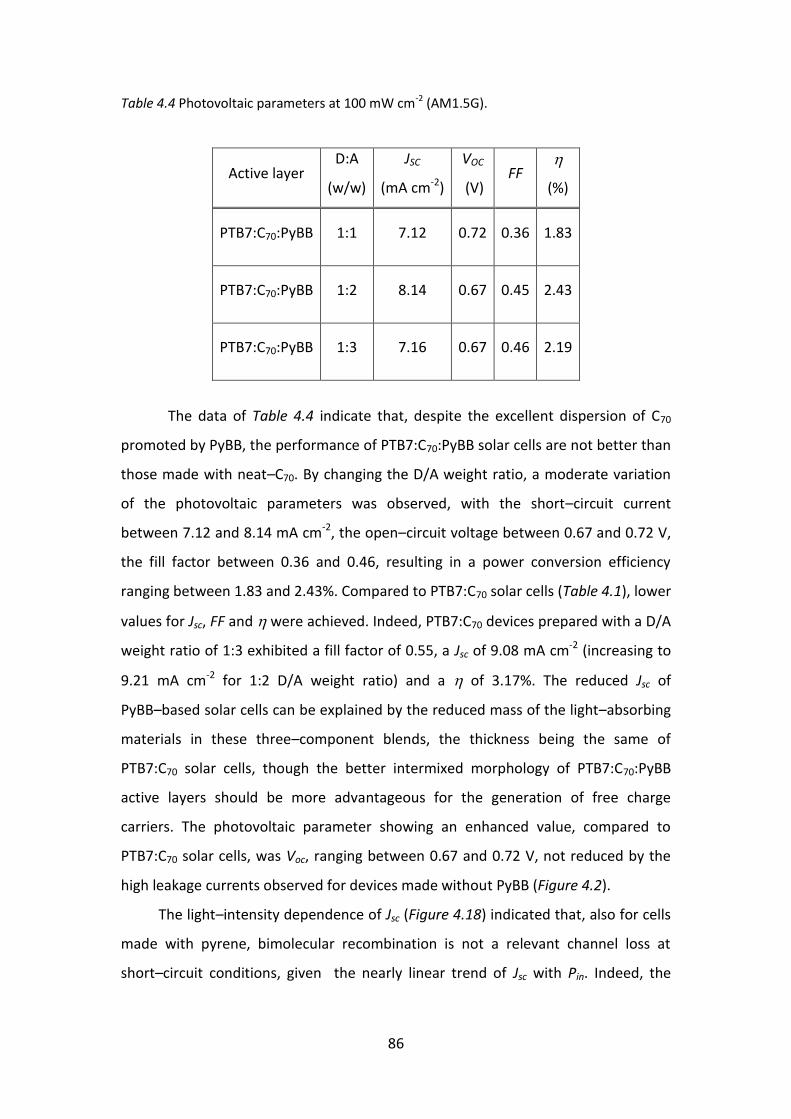
86
Table 4.4 Photovoltaic parameters at 100 mW cm-2 (AM1.5G).
Active layer D:A
(w/w)
JSC
(mA cm-2)
VOC
(V) FF
(%)
PTB7:C70:PyBB 1:1 7.12 0.72 0.36 1.83
PTB7:C70:PyBB 1:2 8.14 0.67 0.45 2.43
PTB7:C70:PyBB 1:3 7.16 0.67 0.46 2.19
The data of Table 4.4 indicate that, despite the excellent dispersion of C70
promoted by PyBB, the performance of PTB7:C70:PyBB solar cells are not better than
those made with neat–C70. By changing the D/A weight ratio, a moderate variation
of the photovoltaic parameters was observed, with the short–circuit current
between 7.12 and 8.14 mA cm-2, the open–circuit voltage between 0.67 and 0.72 V,
the fill factor between 0.36 and 0.46, resulting in a power conversion efficiency
ranging between 1.83 and 2.43%. Compared to PTB7:C70 solar cells (Table 4.1), lower
values for Jsc, FF and were achieved. Indeed, PTB7:C70 devices prepared with a D/A
weight ratio of 1:3 exhibited a fill factor of 0.55, a Jsc of 9.08 mA cm-2 (increasing to
9.21 mA cm-2 for 1:2 D/A weight ratio) and a of 3.17%. The reduced Jsc of
PyBB–based solar cells can be explained by the reduced mass of the light–absorbing
materials in these three–component blends, the thickness being the same of
PTB7:C70 solar cells, though the better intermixed morphology of PTB7:C70:PyBB
active layers should be more advantageous for the generation of free charge
carriers. The photovoltaic parameter showing an enhanced value, compared to
PTB7:C70 solar cells, was Voc, ranging between 0.67 and 0.72 V, not reduced by the
high leakage currents observed for devices made without PyBB (Figure 4.2).
The light–intensity dependence of Jsc (Figure 4.18) indicated that, also for cells
made with pyrene, bimolecular recombination is not a relevant channel loss at
short–circuit conditions, given the nearly linear trend of Jsc with Pin. Indeed, the
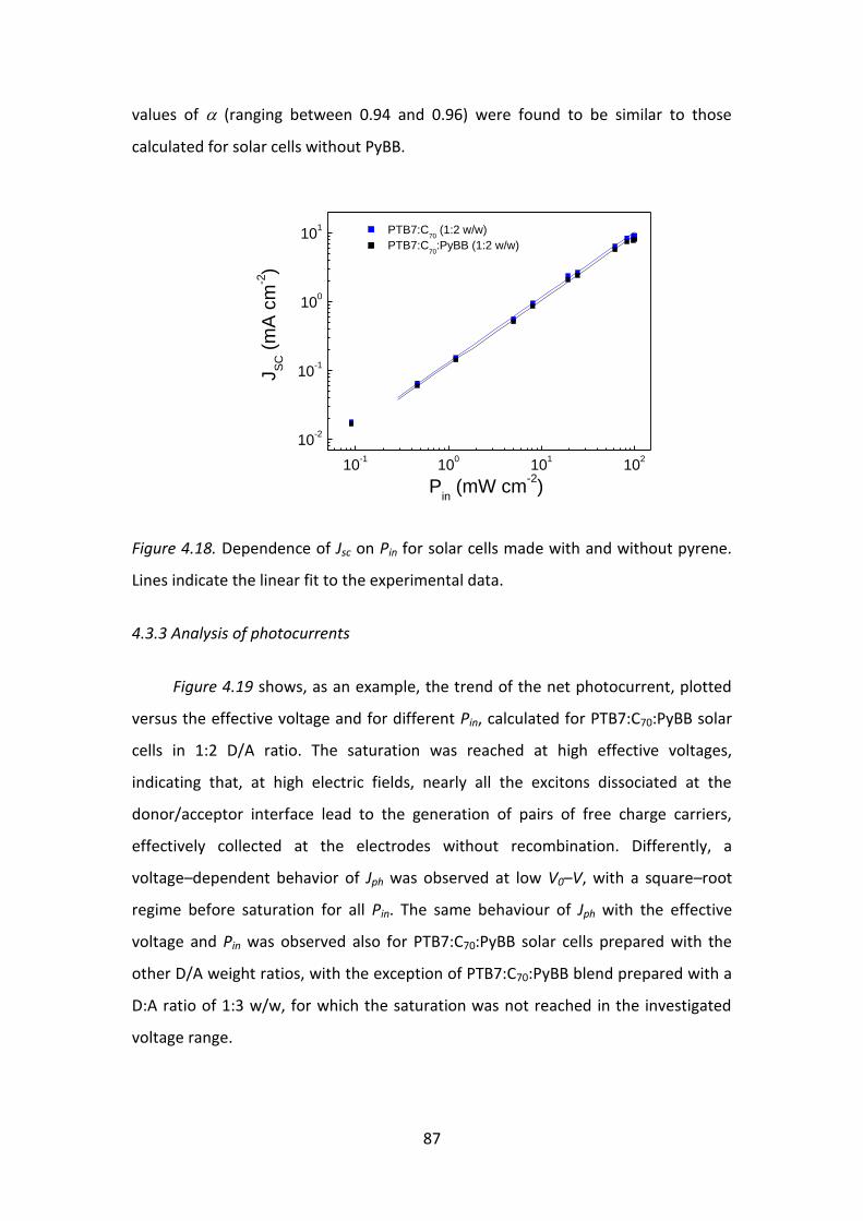
87
values of (ranging between 0.94 and 0.96) were found to be similar to those
calculated for solar cells without PyBB.
10-1
100
101
102
10-2
10-1
100
101 PTB7:C
70 (1:2 w/w)
PTB7:C70
:PyBB (1:2 w/w)
Pin (mW cm
-2)
JS
C (
mA
cm
-2)
Figure 4.18. Dependence of Jsc on Pin for solar cells made with and without pyrene.
Lines indicate the linear fit to the experimental data.
4.3.3 Analysis of photocurrents
Figure 4.19 shows, as an example, the trend of the net photocurrent, plotted
versus the effective voltage and for different Pin, calculated for PTB7:C70:PyBB solar
cells in 1:2 D/A ratio. The saturation was reached at high effective voltages,
indicating that, at high electric fields, nearly all the excitons dissociated at the
donor/acceptor interface lead to the generation of pairs of free charge carriers,
effectively collected at the electrodes without recombination. Differently, a
voltage–dependent behavior of Jph was observed at low V0–V, with a square–root
regime before saturation for all Pin. The same behaviour of Jph with the effective
voltage and Pin was observed also for PTB7:C70:PyBB solar cells prepared with the
other D/A weight ratios, with the exception of PTB7:C70:PyBB blend prepared with a
D:A ratio of 1:3 w/w, for which the saturation was not reached in the investigated
voltage range.
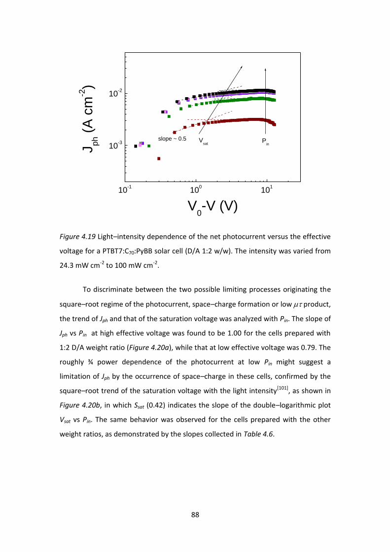
88
Figure 4.19 Light–intensity dependence of the net photocurrent versus the effective
voltage for a PTBT7:C70:PyBB solar cell (D/A 1:2 w/w). The intensity was varied from
24.3 mW cm-2 to 100 mW cm-2.
To discriminate between the two possible limiting processes originating the
square–root regime of the photocurrent, space–charge formation or low product,
the trend of Jph and that of the saturation voltage was analyzed with Pin. The slope of
Jph vs Pin at high effective voltage was found to be 1.00 for the cells prepared with
1:2 D/A weight ratio (Figure 4.20a), while that at low effective voltage was 0.79. The
roughly ¾ power dependence of the photocurrent at low Pin might suggest a
limitation of Jph by the occurrence of space–charge in these cells, confirmed by the
square–root trend of the saturation voltage with the light intensity[101], as shown in
Figure 4.20b, in which Ssat (0.42) indicates the slope of the double–logarithmic plot
Vsat vs Pin. The same behavior was observed for the cells prepared with the other
weight ratios, as demonstrated by the slopes collected in Table 4.6.
10-1
100
101
10-3
10-2
Pin
Vsat
slope ~ 0.5
Jph (
A c
m-2)
V0-V (V)

89
Figure 4.20 Light–intensity dependence of the photocurrent (a) and the saturation voltage
(b) for a PTB7:C70:PyBB device (D/A 1:2 w/w). Lines indicate the linear fit to the
experimental data. The values of the slopes are also reported.
Table 4.6 Slopes of the double–logarithm plots Jph vs. Pin and Vsat vs. Pin
Active layer D:A
(w/w) SLB SHB Ssat
PTB7:C70:PyBB 1:1 0.77 0.94 0.46
PTB7:C70:PyBB 1:2 0.74 0.92 0.52
PTB7:C70:PyBB 1.3 0.74 0.88 --
The values of the slopes of Table 4.6, clearly prove that Jph is limited by the
build–up of space charge in all solar cells prepared with pyrene. This result suggests
that charge carrier mobility in this devices could be strongly unbalanced.
4.3.4 Charge carrier mobility
In order to prove our hypothesis about the strongly unbalanced mobility in
solar cells with pyrene, hole–only and electron–only PTB7:C70:PyBB devices were
prepared as described in paragraph 2.1.1, to measure the charge carrier mobility
with the SCLC technique. The best fit of the experimental data was obtained by
using the Mott–Gurney law modified for dependent on field (equation 2.3). The
parameters extracted from the fit of the J–V curves are collected in Table 4.7.
102
10-3
10-2
(a)
SHB
=0.92
V0-V=9V
SLB
=0.74
V0-V=0.4VJ
ph (
A c
m-2)
Pin (mW cm
-2)
102
100
(b)
Ssat
=0.52
Vsat (
V)
Pin (mW cm
-2)
90
Table 4.7 Hole and electron mobility (calculated for an electric field of 105 V cm-1) and
parameter for PTB7:C70:PyBB blends.
Active layer D:A
(w/w)
μh
(cm2 V-1 s-1)
μe
(cm2 V-1 s-1)
h
(cm1/2 V-1/2)
e
(cm1/2 V-1/2)
PTB7:C70:PyBB 1:1 5.49 × 10⁻⁵ 5.21 × 10⁻⁷ 2.90 × 10⁻⁴ 1.30 × 10⁻²
PTB7:C70:PyBB 1:2 4.28 × 10⁻⁵ 4.57 × 10⁻⁷ -- 1.20 × 10⁻²
PTB7:C70:PyBB 1:3 2.72 × 10⁻⁵ 5.67 × 10⁻⁷ 4.00 × 10⁻⁴ 1.40 × 10⁻²
Despite the clear morphological variation, the mobility of holes does not
undergo significant variations in the devices with pyrene, compared with solar cells
prepared without PyBB (Table 4.3). The hole mobility was between 2.72×10⁻⁵ and
5.49×10⁻⁵ cm2 V-1 s-1 by changing the D/A ratio of PTB7:C70:PyBB blends. Differently,
the mobility of negative carriers was found to be drastically reduced, in comparison
with that of PTB7:C70 cells. Mobility values between 4.57×10⁻⁷ and
5.67×10⁻⁷ cm2 V-1 s-1 were obtained for electrons, that is, roughly two orders of
magnitude lower than in solar cells without PyBB. In addition, a strong dependence
of the electron mobility on the electric field was also observed, as demonstrated by
the high values of e.
In spite of the presence of pyrene, solar cells with PyBB showed strongly
unbalanced hole and electron mobility. This condition results favourable for the
formation of space charge, as confirmed by the behaviour observed for the
photocurrent. For these cells, negative charge carriers are much slower than positive
ones and tend to be accumulated in the device. The accumulation of charge favours
the bimolecular recombination processes, with consequent loss of the device
performance.
4.3.5 Impedance spectra
The impedance spectra obtained under 100 mW cm-2 illumination for
PTB7:C70:PyBB devices are displayed in Figure 4.21 and compared with that of a cell
without pyrene. The Nyquist plots of PTB7:C70:PyBB cells exhibited a major arc in the
low frequency range and a smaller one toward high frequency. For comparison, the
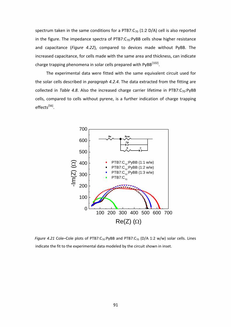
91
spectrum taken in the same conditions for a PTB7:C70 (1:2 D/A) cell is also reported
in the figure. The impedance spectra of PTB7:C70:PyBB cells show higher resistance
and capacitance (Figure 4.22), compared to devices made without PyBB. The
increased capacitance, for cells made with the same area and thickness, can indicate
charge trapping phenomena in solar cells prepared with PyBB[102].
The experimental data were fitted with the same equivalent circuit used for
the solar cells described in paragraph 4.2.4. The data extracted from the fitting are
collected in Table 4.8. Also the increased charge carrier lifetime in PTB7:C70:PyBB
cells, compared to cells without pyrene, is a further indication of charge trapping
effects[56].
100 200 300 400 500 600 7000
100
200
300
400
500
600
700
PTB7:C70
:PyBB (1:1 w/w)
PTB7:C70
:PyBB (1:2 w/w)
PTB7:C70
:PyBB (1:3 w/w)
PTB7:C70
-Im
(Z)
()
Re(Z) ()
Figure 4.21 Cole–Cole plots of PTB7:C70:PyBB and PTB7:C70 (D/A 1:2 w/w) solar cells. Lines
indicate the fit to the experimental data modeled by the circuit shown in inset.

92
103
104
105
106
10-9
10-8
10-7
Ca
pacita
nce
(F
)
Frequency (Hz)
PTB7:C70
(1:2 w/w)
PTB7:C70
:PyBB (1:2 w/w)
Figure 4.22 Capacitance as a function of the frequency in PTB7–based solar cells. The D/A
weight ratio is indicated in parenthesis.
Table 4.9 Parameters extracted from the fit of Cole–Cole plots at 1 sun.
Active layer D:A
(w/w)
Rrec
()
Cµ
(nF)
(s)
PTB7:C70 1:2 231.5 7.2 1.7
PTB7:C70:PyBB 1:1 590.3 9.9 5.9
PTB7:C70:PyBB 1:2 495.4 56.6 28.0
PTB7:C70:PyBB 1:3 535.4 46.8 25.1
The impedance measurements were performed at different levels of the light power
intensity, in order to get indication on the order of charge recombination processes
in the investigated cells. It has been shown that Rrec is related to Voc, dependent on
Pin, through the following expression:
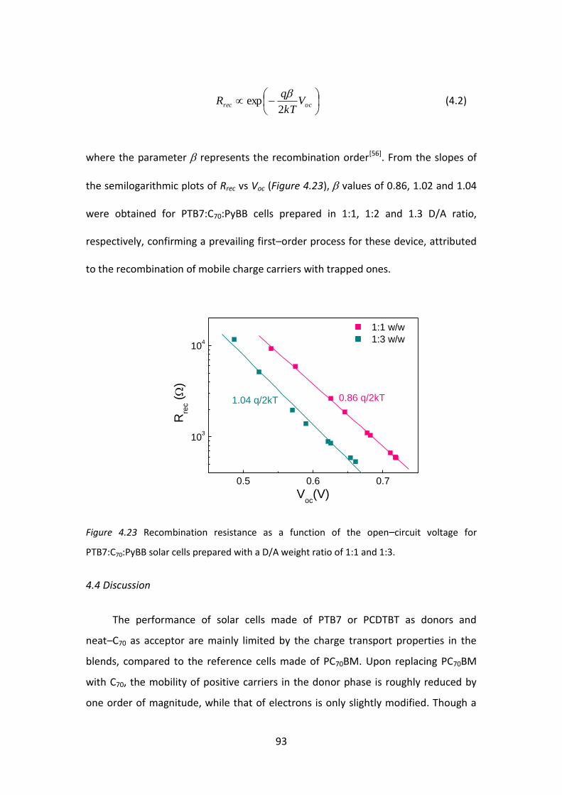
93
ocrec V
kT
qR
2exp
(4.2)
where the parameter represents the recombination order[56]. From the slopes of
the semilogarithmic plots of Rrec vs Voc (Figure 4.23), values of 0.86, 1.02 and 1.04
were obtained for PTB7:C70:PyBB cells prepared in 1:1, 1:2 and 1.3 D/A ratio,
respectively, confirming a prevailing first–order process for these device, attributed
to the recombination of mobile charge carriers with trapped ones.
0.5 0.6 0.7
103
104
1.04 q/2kT 0.86 q/2kT
1:1 w/w
1:3 w/w
Rre
c (
)
Voc
(V)
Figure 4.23 Recombination resistance as a function of the open–circuit voltage for
PTB7:C70:PyBB solar cells prepared with a D/A weight ratio of 1:1 and 1:3.
4.4 Discussion
The performance of solar cells made of PTB7 or PCDTBT as donors and
neat–C70 as acceptor are mainly limited by the charge transport properties in the
blends, compared to the reference cells made of PC70BM. Upon replacing PC70BM
with C70, the mobility of positive carriers in the donor phase is roughly reduced by
one order of magnitude, while that of electrons is only slightly modified. Though a
94
strong unbalanced transport was not observed in C70–based cells, preventing
space–charge formation, a limitation of the photocurrent due to a low product
was systematically observed, independently of the polymer donor and the D/A ratio.
The effective lifetime of charge carriers did not change a lot by replacing PC70BM
with C70, though was slightly reduced in neat–C70 solar cells, but, combined with the
lower mobility, contributed to the significant reduction of the product in devices
made of neat–C70, compared to PC70BM-based solar cells.
The modified charge transport properties of C70–based cells were determined
by the blend morphology, affected by the replacement of the acceptor. A highly
segregated morphology was observed for PTBT:C70 solar cells, with the formation of
large domains with a size of hundreds of nm. Given the worse mobility of holes in
these blends, poorly interconnected domains in the donor phase can be
hypothesized. Differently, PCDTBT was an excellent dispersant for C70 and the
comparison of the surface morphology of PCDTBT:C70 and PCDTBT:PC70BM blends
did not reveal significant differences, at least on the scale explored by the AFM.
However, despite the relevant different morphologies of C70–based blends made of
the two polymers, a consistent reduction of the hole mobility was also observed for
PCDTBT:C70 solar cells, indicating that the D/A mixing is not so effective in the
formation of the bicontinuous donor and acceptor domains required for efficient
charge transport.
Nevertheless, thanks to the enhanced light absorption of the blends made of
neat–C70, PCDTBT:C70 solar cells underwent a limited loss of efficiency (~ 5%),
compared to the reference PCDTBT:PC70BM, reaching a of 4.55% and
demonstrating that high efficiency solar cells made of cheap neat–fullerene are
possible if the right donor is selected.
In order to obtain a better dispersion of C70 in PTB7, a third component, PyBB,
was introduced in the blends. The effectiveness of PyBB as dispersant of C70 is clearly
demonstrated by the AFM images. Indeed, the morphology of PTB7:C70:PyBB blends
does not show the formation of the micrometric agglomerates observed without
PyBB. However, despite the huge morphological variation obtained with PyBB
dispersant, the performance of PTB7:C70:PyBB solar cells were not significantly
improved with respect to those made without PyBB. The best performance was

95
obtained for the D/A ratio of 1:2 w/w, with an efficiency at one sun of 2.43%, to be
compared with 2.22% obtained without pyrene.
The extended electrical characterization indicated that the main limiting
factors of PyBB–based solar cells, both correlated to inadequate charge transport
properties, are: space charge formation and charge trapping effects. Charge
trapping is, at least in part, responsible for the drastic reduction of electron mobility
in PTB7:C70:PyBB solar cells. As a consequence, the strongly unbalanced hole and
electron mobilities, differing by two orders of magnitude, lead to the formation of
space charge, with a loss of performance for solar cells containing PyBB.
The origin of charge trapping upon addition of PyBB in the active layer is still
under investigation.
96
CHAPTER 5 – CONCLUDING REMARKS
Charge transport properties constitute a major determining factor for the
operation of any electronic device and mainly for organic electronics, given the
much worse mobility of charge carriers in organic materials, compared to that in
conventional semiconductors. On the other hand, charge carrier mobility in organic
solids is highly dependent on a number of factors (chemical structure, deposition
conditions, and macromolecular parameters for polymers), as demonstrated in this
Thesis for AnE–PVs conjugated polymers, which must be accurately controlled in
order to obtain good performance for electronic applications.
AnE–PVs are a relevant class of conjugated polymers. By appropriately
choosing the lateral side–chains and the deposition conditions, affecting the
electronic interaction between the conjugated backbones and the order degree of
the film, hole and electron mobilities of the order of 10-4 and 10-3 cm2 V-1 s-1 have
been achieved, respectively. In addition, even a moderate variation of the molecular
weight (just of a factor of two) has been found to induce a meaningful modification
of charge carrier mobility, as well as of the optical properties of the polymer films.
Interestingly, all investigated AnE–PVs show a very good ambipolar behaviour,
demonstrated for the first time in this Thesis work.
For the photovoltaic application, the correlation between charge transport
properties and device performance is much more critical than for other organic
devices, given the particular arrangement of the donor and acceptor phases in the
active layer of BHJ solar cells. As a consequence, charge carrier mobility in the two
different phases of the donor/acceptor blend is highly determined by the blend
morphology, in addition to that exhibited by the pristine materials, and most of the
losses of BHJ solar cells are currently due to low and/or unbalanced mobilities.
Concerning the intrinsic charge transport properties of pristine photovoltaic
materials, a straight correlation between hole mobility in pristine AnE–PVs and the
fill factor of the related solar cells, using PCBM as acceptor, has been found.
However, the great impact of charge transport for the performance of BHJ solar cells
is more clearly demonstrated by the results obtained on BHJ solar cells made of
97
neat–C70, instead of its soluble derivatives. The aim of the work was to give a
contribution to further restrain the costs of active materials, low cost being one of
the main advantages of this innovative photovoltaic technology.
The performance of solar cells made of PTB7 or PCDTBT as donors and
neat–C70 as acceptor are mainly limited by the charge transport properties in the
blends, compared to the reference cells made of PC70BM. Upon replacing PC70BM
with C70, the mobility of positive carriers in the donor phase is roughly reduced by
one order of magnitude, while that of electrons is only slightly modified. Though a
strong unbalanced transport was not observed in C70–based cells, preventing
space–charge formation, a limitation of the photocurrent due to a low product
was systematically observed, independently of the polymer donor and the D/A ratio.
The modified charge transport properties in the C70–based cells were determined by
the blend morphology, affected by the replacement of the acceptor. A highly
segregated morphology was observed for PTBT:C70 solar cells, with the formation of
large domains with a size of hundreds of nm. Differently, PCDTBT was an excellent
dispersant for C70 and the comparison of the surface morphology of PCDTBT:C70 and
PCDTBT:PC70BM blends did not reveal significant differences. However, despite the
relevant different morphologies of C70–based blends made of the two polymers, a
consistent reduction of the hole mobility was also observed for PCDTBT:C70 solar
cells, indicating that the D/A mixing is not so effective in the formation of the
bicontinuous donor and acceptor domains required for efficient charge transport.
Nevertheless, PCDTBT:C70 solar cells underwent a limited loss of efficiency (12%),
compared to the reference PCDTBT:PC70BM, reaching an efficiency of 4.22% and
demonstrating that high efficiency solar cells made of cheap neat–fullerene are
possible if the right donor is selected.
The introduction of a third component in the blends, a derivative of pyrene,
was greatly effective in improving the dispersion of C70 in the PTB7 matrix, but a
consequent improvement of the performance of the related solar cells was not
observed. The strong unbalanced mobilities led to space–charge formation in the
blends with pyrene and charge trapping effects were also found.

98
LIST OF PUBLICATIONS
1. Nadia Camaioni, Francesca Tinti, Alessandra Degli Esposti, Sara Righi, Ozlem Usluer,
Sameh Boudiba, and Daniel A. M. Egbe “Electron and hole transport in an
anthracene–based conjugated polymer” APPLIED PHYSICS LETTERS, 101, 053302
(2012)
2. Francesca Tinti, Fedlu K. Sabir, Massimo Gazzano, Sara Righi, Christoph Ulbricht,
Ozlem Usluer, Veronika Pokorna, Vera Cimrova, Teketel Yohannes, Daniel A.M. Egbe
and Nadia Camaioni “Tuning the properties of an anthracene–based PPE–PPV
copolymer by fine variation of its macromolecular parameters” RSC Advances, 3,
6972 (2013)
3. Francesca Tinti, Fedlu K. Sabir, Massimo Gazzano, Sara Righi, Christoph Ulbricht,
Ozlem Usluer, Teketel Yohannes, Daniel A.M. Egbe and Nadia Camaioni “Effect of
Side Chains on Charge Transport of Anthracene-Based PPE–PPV Copolymers”
DOI:10.1002/macp.201300611
4. Nicola Gasparini, Sara Righi, Francesca Tinti, Alberto Savoini, Riccardo Po and Nadia
Camaioni “Efficient bulk–heterojunction solar cells with neat C70” submitted.
5. Nicola Gasparini, Sara Righi, Francesca Tinti, Alberto Savoini,Riccardo Po and Nadia
Camaioni “Charge trapping in PTB7:C70:pyrene bulk–heterojunctsolar cells” in
preparation.

99
REFERENCES
[1] http://www.rsc.org/ScienceAndTechnology/roadmap/CS3-2013.asp
[2] B. D. Malhotra, et. al., Pramana – J. Phys., 61, 331 (2003).
[3] P. Sonar, et. al., Phys. Chem. Chem. Phys., 15, 17064 (2013).
[4] H. Yan, et. al., Nature, 457, 679 (2009).
[5] I. Mc Culloch, et. al., Nature Mater., 5, 328 (2006).
[6] H. Sirringhaus, et. al., Nature, 401, 685 (1999).
[7] Worldwide Organic Electronics Market ww.productronica.com (1999).
[8] W. Brutting, et. al., Physics of Organic Semiconductors, Wiley-VCH (2005) cap. 1.
[9] T. A. Skotheim, et. al., Handbook of Conducting Polymers, Marcel Dekker (1998).
[10] V. Coropceanu, et. al., Chem. Rev.,107, 926 (2007).
[11] S. Holliday, et. al., Chem. Mater., DOI: 10.1021/cm402421p.
[12] J. L. Bredas et. al., J. Chem. Rev., 104, 4971 (2004).
[13] A. J. Mozer, et.al., J. Phys. Chem. B, 108, 5235 (2004).
[14] D. M. Pai, J. Chem. Phys., 52, 2285 (1970).
[15] W. D. Gill, J. Appl. Phys., 43, 5033 (1972).
[16] H. Poole, Phylos. Mag., 32, 112 (1916).
[17] J. Frenkel, Phys. Rev., 54, 647 (1938).
[18] H. Bässler, Phys. Status Solidi B, 175, 15 (1993).
[19] A. W. Hains, et. al., Chem. Rev., 110, 6689 (2010).
[20] Y. Sun, et. al., Nat. Mater., 11, 44 (2012).
[21] S. Gunes, et. al., Chem. Rev., 107, 1324 (2007).
[22] R. Po, et. al., Energy Environ. Sci., 4, 285 (2011).
[23] R. Po, et. al., J. Phys. Chem., 114, 695 (2010).
[24] R. Po, et. al., J. Phys. Chem. Lett., 4, 1821 (2013)
[25] G. Yu, et. al., J. Appl. Phys., 78, 4510 (1995).
[26] J. J. M. Halls, et. al., Nature, 376, 49 (1995)
[27] B. C. Thompson, et. al., Angew. Chem. Int. Ed., 47, 58 (2008).
[28] P. T. Boudreault, et. al., Chem. Mater., 23, 456 (2011).
[29] M. T. Dang, et. al., Chem. Rev., 113, 3734 (2013).
100
[30] M. A. Green, et. al., Prog. Photovoltaics: Res. Appl., 21, 1 (2013).
[31] H. J. Park, et. al., Energy Environ. Sci., 6, 2203 (2013).
[32] L. J. A. Koster, et. al., Appl. Phys. Lett., 88, 052104 (2006).
[33] J. D. Servaites, et. al., Energy Environ. Sci., 4, 4410 (2011).
[34] H. Azimi, et. al., Adv. Energy Mater., 1, 1162 (2011).
[35] E. Von Hauff, et. al., Sol. Energy Mater. Sol. Cells, 87, 149 (2005).
[36] K. N. Semenov, et. al., J. Chem. Eng. Data, 55, 13 (2010).
[37] M. A. Lampert , et. al., Current Injection in Solids Academic, New York (1970).
[38] D. Gupta, et. al., Proceedings of the IEEE, 97, 1558 (2009).
[39] S. Bange, et. al., Phys. Rev. B, 81, 035209 (2010).
[40] K. Kassing, Phys. Status Solidi, 28, 107 (1975).
[41] C. J. Brabec, et. al., Appl. Phys. Lett, 80, 7 (2002).
[42] W. E. Spear, Proc. Phys. Soc. B, 70, 1139 (1957).
[43] W. E.Spear, Proc. Phys. Soc., 76, 826 (1960).
[44] O. H. Le Blanc, J. Chem. Phys., 33, 626 (1960).
[45] R. G. Kepler, Phys. Rev., 119, 1226 (1960).
[46] D. Poplavskyy, et. al., J. App. Phys. 93, 341 (2003).
[47] R. Schwarz, J. Non–Cryst. Solids, 227, 148 (1998).
[48] J. R. Macdonald, et. al., Impedance Spectroscopy Theory, Experiment, and
Applications, Wiley–Interscience (2005).
[49] P. W. M. Blom et. al., Synth. Met., 121, 1621 (2001).
[50] A. Foertig, et.al., Phys. Rev. B, 86, 115302 (2012).
[51] C. J. Brabec, et. al., Adv. Funct. Mater., 12, 709 (2002).
[52] A. Gadisa, et. al., Appl. Phys. Lett., 84, 1609 (2004).
[53] V. D. Mihailetchi, et. al., Appl. Phys. Lett., 93, 216601 (2004).
[54] M . Lenes, et. al., Adv. Funct. Mater., 19, 1106 (2009).
[55] G. Garcia–Belmonte, et. al., Sol. Energy Mater. & Sol. Cells, 94, 366 (2010).
[56] A. J. Heeger, et. al., Adv. Energy Mater., 1, 517 (2011).
[57] D. A. M. Egbe, et.al., Macromolecules, 43, 1261 (2010).
[58] Ö. Usluer, et. al., J. Polym. Sci. Polym. Chem., 50, 3425 (2012).
[59] P. A. Troshin, et. al., Adv. Energy Mater, 3, 161 (2013).
101
[60] S. Saeb, et.al., TEOCHEM, 200, 361 (1989).
[61] M. Levitus, et. al., J. Am. Chem. Soc.,123, 4259 (2001).
[62] D. A. M. Egbe, et.al., Prog. Polym. Sci.,34, 1023 (2009).
[63] G. D. Sharma, et. al., Appl. Mater. & Interface, 2, 504 (2010).
[64] D. A. M. Egbe, et.al., J. Mater. Chem., 20, 972 (2010).
[65] A. D. Becke, J. Chem. Phys., 98, 5648 (1993).
[66] S. Rathgeber, et.al, Macromolecules, 43, 306 (2010).
[67] A. J. Campbell, et.al., Appl. Phys. Lett., 79, 2133 (2001).
[68] A. J. Campbell, et.al., J. Appl. Phys., 82, 6326 (1997).
[69] H. Scher et al., Phys. Rev.B, 12, 2455 (1975).
[70] P. E. Parris, et al., Phys. Status Solidi B, 218, 47 (2000).
[71] A. Zen, et. al., Adv. Funct. Mater., 14, 757 (2004).
[72] C. Di, et. al., Adv. Mater., 22, 1273 (2010).
[73] L. Pautmeier, et. al., Synth. Met., 37, 371 (1990).
[74] P. M. Borsenberger, et.al., J. Chem. Phys., 94, 5447 (1991).
[75] S. M. Tuladhar, et. al., Phys. Rev. B, 79, 03520 (2009).
[76] H. S. Lee, et.al., J. Phys. Chem. C, 117, 11764 (2013).
[77] H. Bässler, et. al., Top. Curr. Chem., 1, 312 (2012).
[78] T. Tiedje, et. al., Solid State Commun., 37, 49 (1981).
[79] H. Scher, et. al., Phys. Rev. B, 12, 2455 (1975).
[80] S. Rathgeber, et.al., Polymer, 52, 3819 (2011).
[81] R. C. Hiorns, et. al., Adv. Funct. Mater., 16, 2263 (2006).
[82] N. Camaioni, et. al., Appl. Phys. Lett., 101, 053302 (2012).
[83] G. Li, et. al., Nat. Photonics, 6, 153 (2012).
[84] C. J.Brabec, et. al., Adv. Funct. Mater., 11, 374 (2001).
[85] D.E. Motaung, et. al., Sol. Energy Mater. Sol. Cells, 93, 1674 (2009).
[86] M. M. Wienk, et. al., Angew. Chem., Int. Ed., 42, 3371 (2003).
[87] N. Blouin et. al., Adv. Mater., 19, 2295 (2007).
[88] B. A. Collins, et. al., Adv. Energy Mater., 3, 65 (2013).
[89] G. Namkoong, et. al., Org. Electr., 14, 74 (2013).
[90] M. C. Scharber, et. al., Adv. Mater., 18, 789 (2006).
[91] A. M. Goodman, et. al., J. Appl. Phys., 42, 2823 (1971).
102
[92] T. Wang, et. al., Adv. Funct. Mater., 22, 1399 (2012).
[93] P. W. M. Bloom, et. al., Adv. Mater., 19, 1551 (2007).
[94] V. D. Mihailetchi, et. al., Phys. Rev. Lett., 94, 126602 (2005).
[95] H. Azimi, et. al., Adv. Energy Mater., 1, 1162 (2011).
[96] Z. He, et. al., Adv. Mater., 23, 4636 (2011).
[97] A. Mani, et. al., J. Phys. Chem. B, 112, 10086 (2008).
[98] H. Zhou, et. al., Adv. Mater., 25, 1646 (2013).
[99] G.J. Bahun,et. al., J. Polym. Sci. A: Polym. Chem., 48, 1016 (2010).
[100] P.D. Tran, et. al., Angew. Chem. Int. Ed., 50, 1371 (2011).
[101] V.D. Mihailetchi, et. al., Adv. Func. Mat.,16, 699 (2006).
[102] A. Guerrero, et. al., Org. Electr., 13, 2326 (2012).

103
ACKNOWLEDGEMENTS
I would first like to acknowledge my assistant supervisor Dr. Nadia Camaioni
for all the care and time she liked to spend in my Ph.D. education. She is an inspiring
example of excellent professional attitude, honesty, and objectivity, which are
qualities every good scientist should never lack. I thank her for helping me and for
being always willing to explain and research.
I would like to thank my supervisor Prof. Stefano Stagni for his good will and
his helpfulness.
My special thanks go to Francesca, Nicola and Roberta for their friendship and
their moral support.
I recognize with gratitude the Research Center for non Conventional Energies,
Istituto ENI Donegani, ENI S.p.A and the Consortium MIST E-R for the economic
support.
Finally, my deepest thanks go to my family and friends whose unwavering love
and irreplaceable presence have guided me throughout.


![Novel Thieno[3,4-b]pyrazine Based π-Conjugated Polymers](https://img.pdfslide.tips/doc/110x75/627dccb84f1cae76452c1a83/novel-thieno34-bpyrazine-based-conjugated-polymers-.jpg)
