Embed Size (px)
Citation preview
1
CHAPTER 1
INTRODUCTION
This industrial training is the training for the student in a period of time in
order to let them have some working experience. It is also essential for practical
evaluation to decide whether the students are worthy to receive the certificate.
Besides that, all their activities and task been given during the training session must
be recorded in the log book been provided. The chances that are given by the
University are good opportunity for the students to let them gather knowledge and
experience as much as they could in the 16 weeks of training period.
This is a better chance for them being exposed to the working experience before
graduating in their studies. Student also gets to study about safety precautions when
working in industries. They also are being exposed about the hazard of working with
the engineering professions that usually are popular for accident tragedies.
2
1.1 Objective of Industrial Training
Among the objective of industrial training are :
1. Apply engineering methods such as design and problems solving.
2. Develop understanding of the functioning and organisation of a business.
3. Develop technical, interpersonal and communication skills, both oral andwritten.
4. Study the safety and hazard at workplace and the respective Personal ProtectiveEquipment (PPE).
5. To expose students to working environment in their respective fields, namely as
the first step for student to prepare before entering the working field after
graduate.
6. Able to be discipline and follow all the rules and regulations at work.
7. Fostering teamwork and good communication with employees in the company.
3
1.2 Industrial Training Importance
Industrial training is to expose the students to real jobs and to improve their
knowledge and skills in their respective fields as well as towards producing graduates
who are competent, ethical, professional, competent and creative. In addition, it helps
student to adapt to a challenging environment. With this, students will be more
prepared and confident in their own capabilities. In addition, students can also learn
how to work in groups effectively, and to understand the role of each team member as
well as to foster a sense of responsibility, trust and cooperation between each other..
4
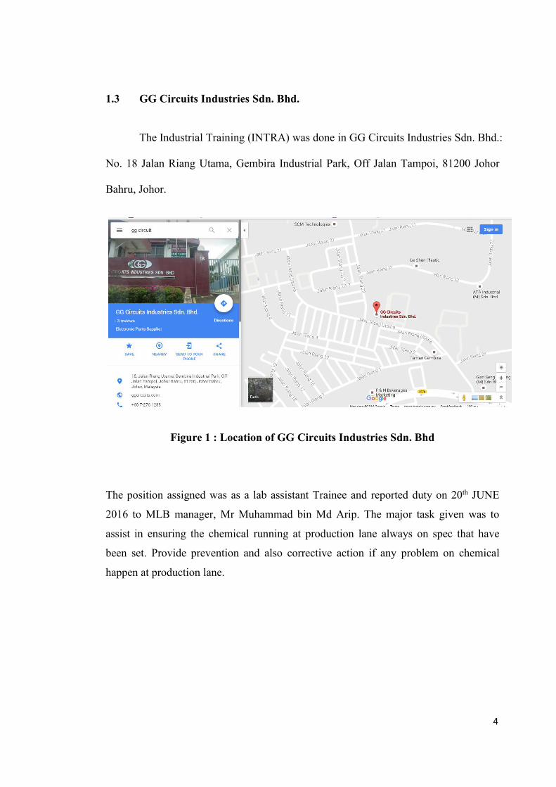
1.3 GG Circuits Industries Sdn. Bhd.
The Industrial Training (INTRA) was done in GG Circuits Industries Sdn. Bhd.:
No. 18 Jalan Riang Utama, Gembira Industrial Park, Off Jalan Tampoi, 81200 Johor
Bahru, Johor.
Figure 1 : Location of GG Circuits Industries Sdn. Bhd
The position assigned was as a lab assistant Trainee and reported duty on 20th JUNE
2016 to MLB manager, Mr Muhammad bin Md Arip. The major task given was to
assist in ensuring the chemical running at production lane always on spec that have
been set. Provide prevention and also corrective action if any problem on chemical
happen at production lane.
5
CHAPTER 2
GG Circuits Industries Sdn. Bhd
2.1 Company Background
GG Circuits Industries Sdn. Bhd. has a relatively long history and recognized tradition,
since its establishment in 1985. Previously, GG Circuits Industries was known as
Golden Glow Enterprise. Figure 2.1 below shows the company logo. Basically, this
company involved in manufacturing of printed circuits board (PCB) for industrial
electronics, automotive, home appliances and communication. Besides, this company
also known globally as one of the advanced in PCB manufacturing for electronics and
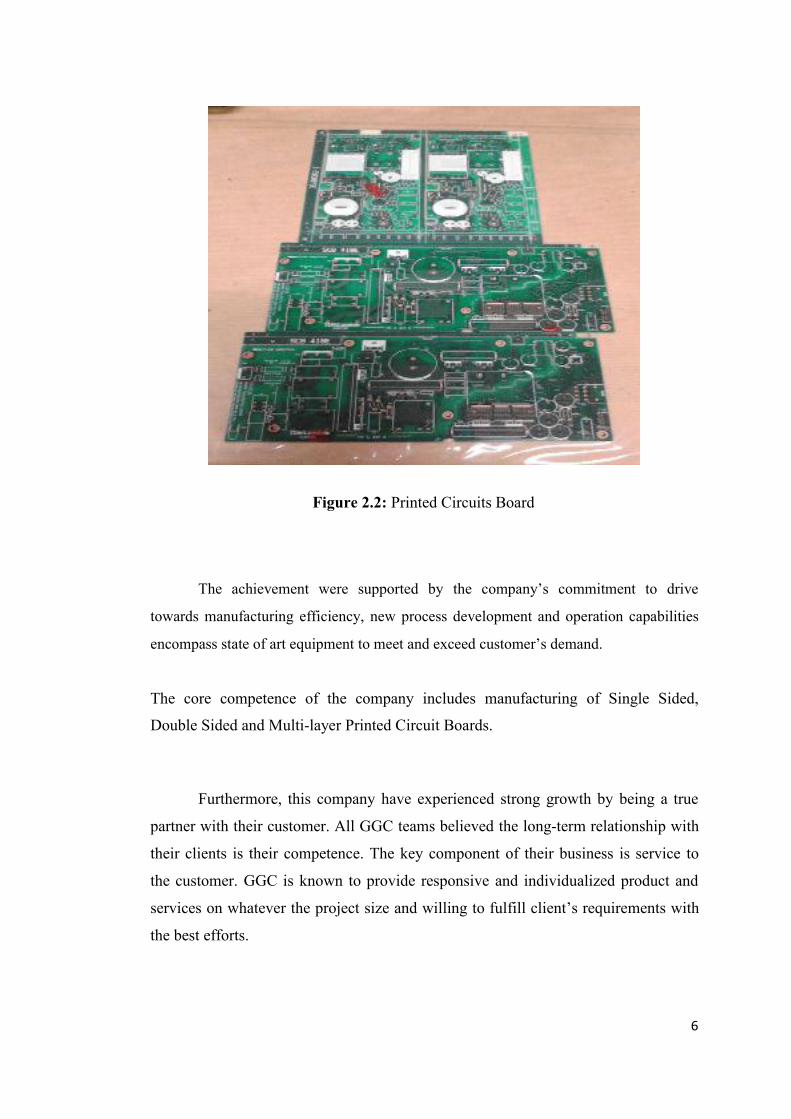
automobile industries. Figure 2.2 shows some PCB’s.
Figure 2.1: Company Logo
6
Figure 2.2: Printed Circuits Board
The achievement were supported by the company’s commitment to drive
towards manufacturing efficiency, new process development and operation capabilities
encompass state of art equipment to meet and exceed customer’s demand.
The core competence of the company includes manufacturing of Single Sided,
Double Sided and Multi-layer Printed Circuit Boards.
Furthermore, this company have experienced strong growth by being a true
partner with their customer. All GGC teams believed the long-term relationship with
their clients is their competence. The key component of their business is service to
the customer. GGC is known to provide responsive and individualized product and
services on whatever the project size and willing to fulfill client’s requirements with
the best efforts.
7
Table 2.1: Details of Company
Name of Company : GG Circuits Industries Sdn. Bhd.
Address : No. 18 Jalan Riang Utama, Gembira Industrial
Park, Off Jalan Tampoi, 81200 Johor Bahru,
Johor
Telephone No. : 07-2761288
Type of business : Manufacturing
Registration No. : 136273-M
Company’s registration date : 5 March 1985
No. of Employee : 200
Products : Printed Circuits Board
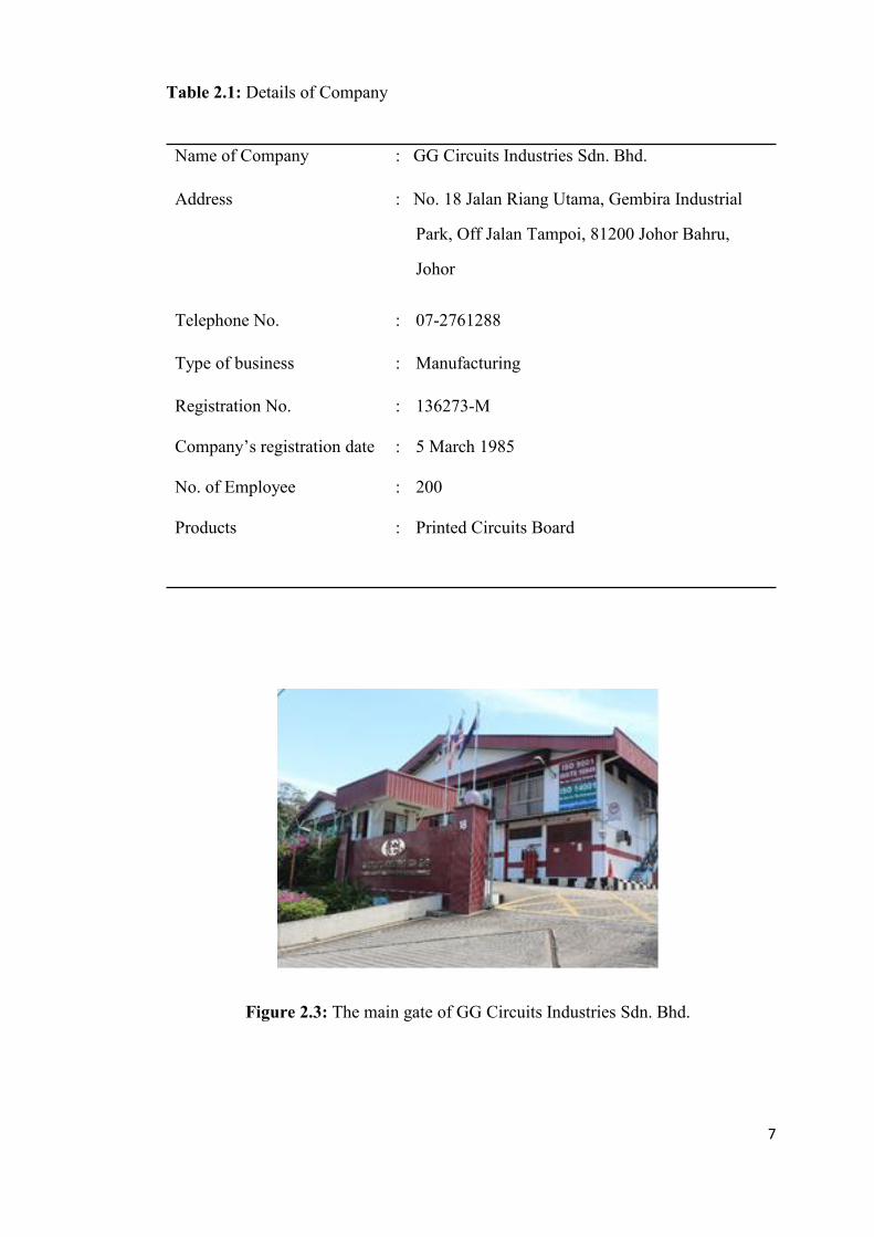
Figure 2.3: The main gate of GG Circuits Industries Sdn. Bhd.
8
4
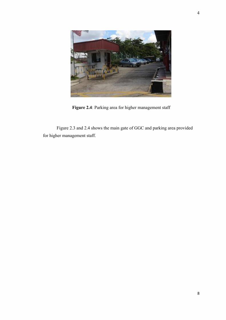
Figure 2.4: Parking area for higher management staff
Figure 2.3 and 2.4 shows the main gate of GGC and parking area provided
for higher management staff.
9
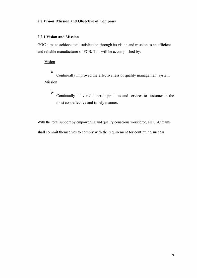
2.2 Vision, Mission and Objective of Company
2.2.1 Vision and Mission
GGC aims to achieve total satisfaction through its vision and mission as an efficient
and reliable manufacturer of PCB. This will be accomplished by:
Vision
Continually improved the effectiveness of quality management system.
Mission
Continually delivered superior products and services to customer in the
most cost effective and timely manner.
With the total support by empowering and quality conscious workforce, all GGC teams
shall commit themselves to comply with the requirement for continuing success.
10
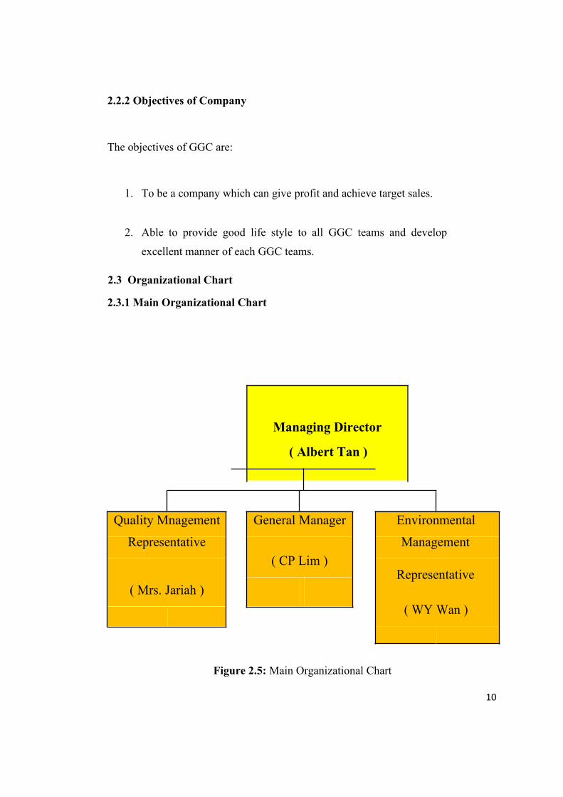
2.2.2 Objectives of Company
The objectives of GGC are:
1. To be a company which can give profit and achieve target sales.
2. Able to provide good life style to all GGC teams and develop
excellent manner of each GGC teams.
2.3 Organizational Chart
2.3.1 Main Organizational Chart
Managing Director
( Albert Tan )
Quality Mnagement General Manager EnvironmentalRepresentative
( CP Lim )Management
( Mrs. Jariah )Representative
( WY Wan )
Figure 2.5:Main Organizational Chart
11
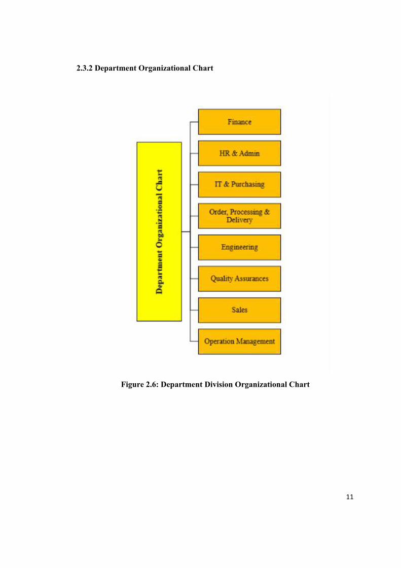
2.3.2 Department Organizational Chart
Figure 2.6: Department Division Organizational Chart
12
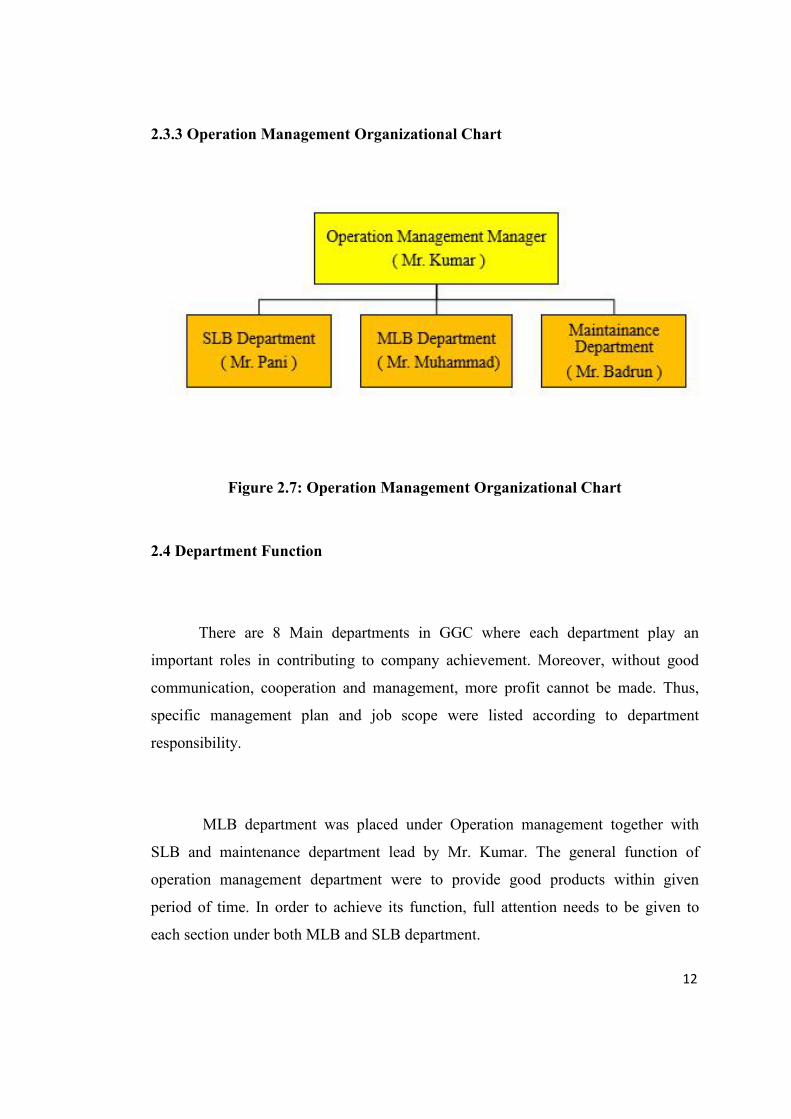
2.3.3 Operation Management Organizational Chart
Figure 2.7: Operation Management Organizational Chart
2.4 Department Function
There are 8 Main departments in GGC where each department play an
important roles in contributing to company achievement. Moreover, without good
communication, cooperation and management, more profit cannot be made. Thus,
specific management plan and job scope were listed according to department
responsibility.
MLB department was placed under Operation management together with
SLB and maintenance department lead by Mr. Kumar. The general function of
operation management department were to provide good products within given
period of time. In order to achieve its function, full attention needs to be given to
each section under both MLB and SLB department.
13
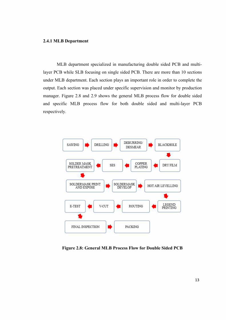
2.4.1 MLB Department
MLB department specialized in manufacturing double sided PCB and multi-
layer PCB while SLB focusing on single sided PCB. There are more than 10 sections
under MLB department. Each section plays an important role in order to complete the
output. Each section was placed under specific supervision and monitor by production
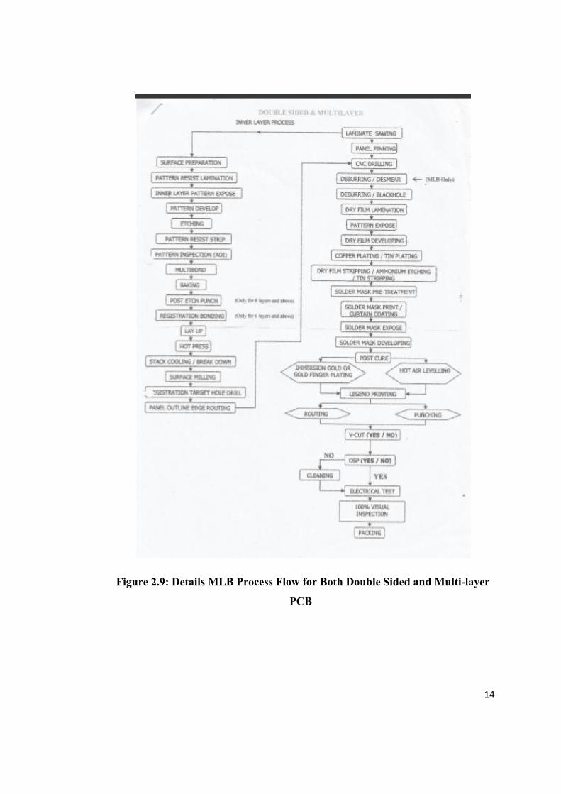
manager. Figure 2.8 and 2.9 shows the general MLB process flow for double sided
and specific MLB process flow for both double sided and multi-layer PCB
respectively.
Figure 2.8: General MLB Process Flow for Double Sided PCB
14
Figure 2.9: Details MLB Process Flow for Both Double Sided and Multi-layer
PCB
15
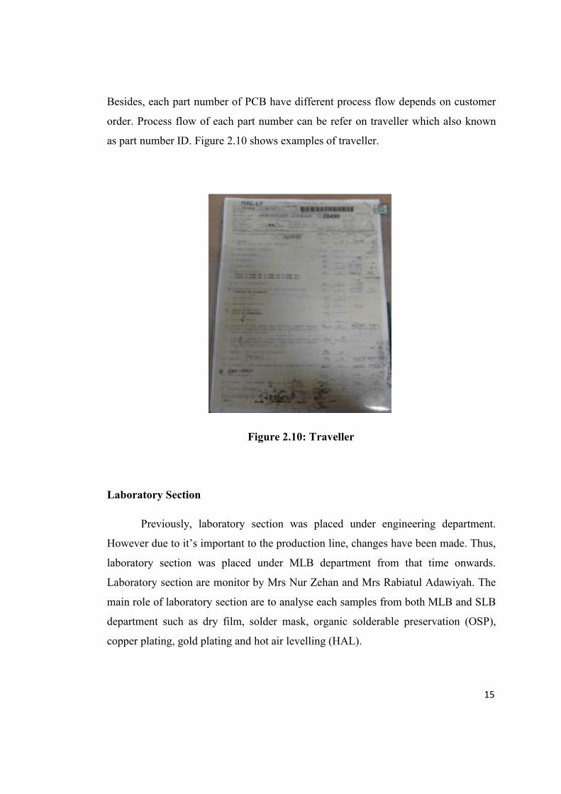
Besides, each part number of PCB have different process flow depends on customer
order. Process flow of each part number can be refer on traveller which also known
as part number ID. Figure 2.10 shows examples of traveller.
Figure 2.10: Traveller
Laboratory Section
Previously, laboratory section was placed under engineering department.
However due to it’s important to the production line, changes have been made. Thus,
laboratory section was placed under MLB department from that time onwards.
Laboratory section are monitor by Mrs Nur Zehan and Mrs Rabiatul Adawiyah. The
main role of laboratory section are to analyse each samples from both MLB and SLB
department such as dry film, solder mask, organic solderable preservation (OSP),
copper plating, gold plating and hot air levelling (HAL).
16
CHAPTER 3
LABORATORY SECTION IN GG CIRCUIT INDUSTRIES SDN. BHD.
3.1 Understanding of Laboratory Responsibility and Scope
3.1.1 Purpose
The purpose of laboratory section is to monitor the chemicals concentration
use in each section under production line. It is important to make sure that all
chemicals were in good condition and enough to support ongoing panels. Besides, as
lab engineer we need to fully understand the method use and chemicals condition in
order to avoid accident.
Furthermore, lab section needs to follow up each samples an hour after
distributed the report or after any replenishment have been made. Sometimes, trainee
also need to follow up samples after new make-up have been made. Normally, each
section will called us and informed regarding new make-up process.
On trainee first day, trainee learned basic analysis which involved titration
method, calibration and observation. There are more than 20 samples that need to be
analysed everyday not including waste water treatment samples (WWTP). Moreover,
trainee have to get used to analyse samples as fast as trainee can since each section
need the chemicals report before run the ongoing panels.
17
3.2 Understanding of MLB Process Flow and its Function
As trainee was placed under MLB department, trainee have to understand the
process involved in PCB manufacturing. According to MLB process engineer, 4
months is not enough for trainee to completely understand every process. . Besides,
during free time trainee learn about the process and output from production lane
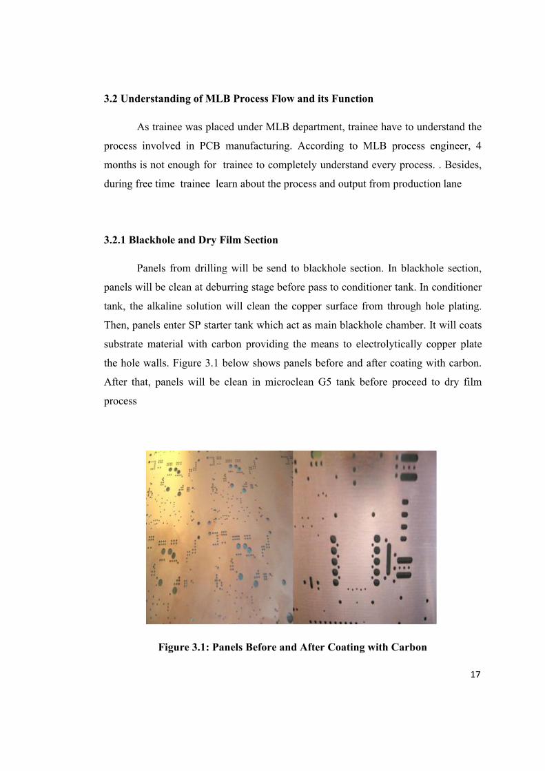
3.2.1 Blackhole and Dry Film Section
Panels from drilling will be send to blackhole section. In blackhole section,
panels will be clean at deburring stage before pass to conditioner tank. In conditioner
tank, the alkaline solution will clean the copper surface from through hole plating.
Then, panels enter SP starter tank which act as main blackhole chamber. It will coats
substrate material with carbon providing the means to electrolytically copper plate
the hole walls. Figure 3.1 below shows panels before and after coating with carbon.
After that, panels will be clean in microclean G5 tank before proceed to dry film
process
Figure 3.1: Panels Before and After Coating with Carbon

18
Dry film consist of lamination, pattern expose and develop stage. In this
section, panels from blackhole will be laminate. After lamination process, pattern
will be exposed on the panels. Before panels went to next section, panels will be
develop in dry film develop to any unwanted resist. Figure 3.2 below shows panels
before and after dry film developing. If panels from dry film developing have
problems and need to redo its process, panels from dry film will be strip in dry film
stripping section.
Figure 3.2: Panels Before and After Dry Film Developing
19
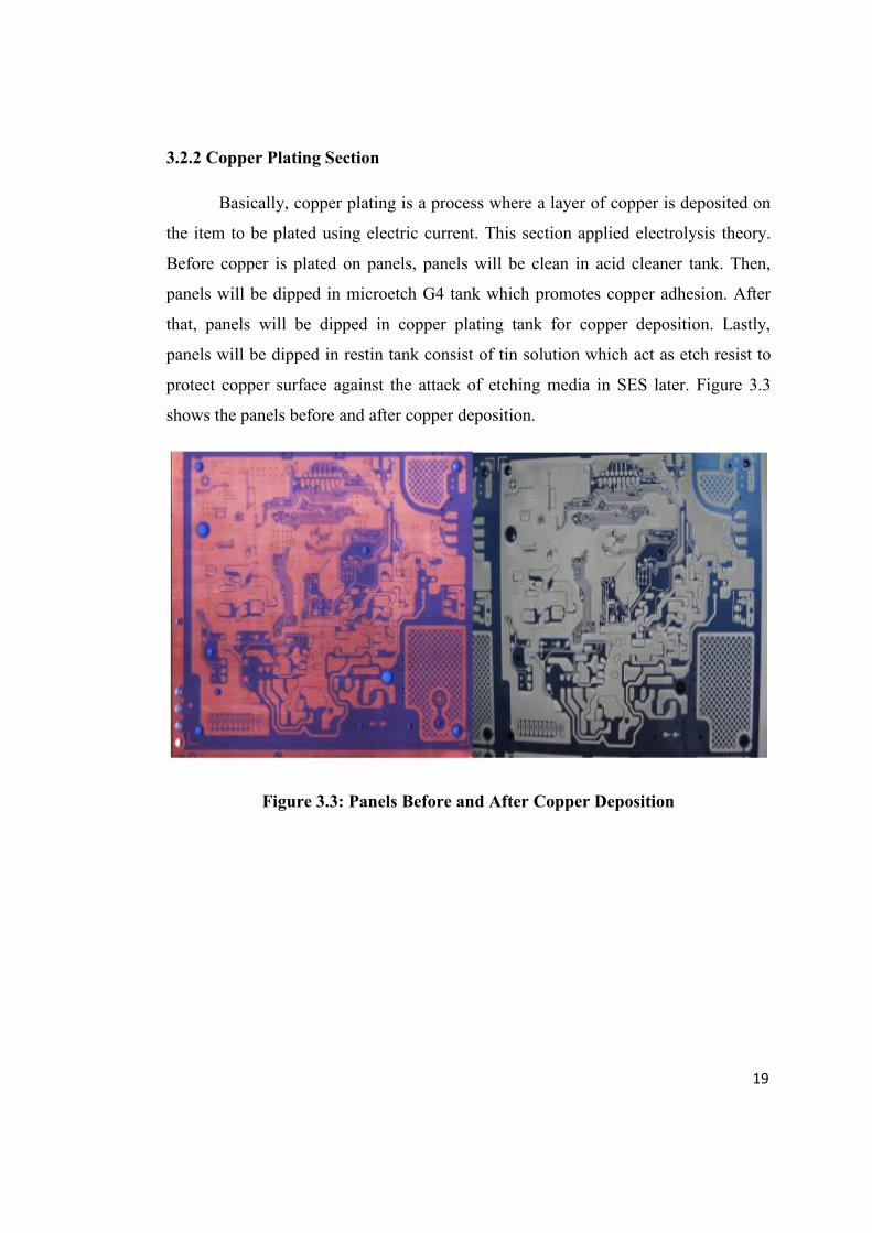
3.2.2 Copper Plating Section
Basically, copper plating is a process where a layer of copper is deposited on
the item to be plated using electric current. This section applied electrolysis theory.
Before copper is plated on panels, panels will be clean in acid cleaner tank. Then,
panels will be dipped in microetch G4 tank which promotes copper adhesion. After
that, panels will be dipped in copper plating tank for copper deposition. Lastly,
panels will be dipped in restin tank consist of tin solution which act as etch resist to
protect copper surface against the attack of etching media in SES later. Figure 3.3
shows the panels before and after copper deposition.
Figure 3.3: Panels Before and After Copper Deposition
20
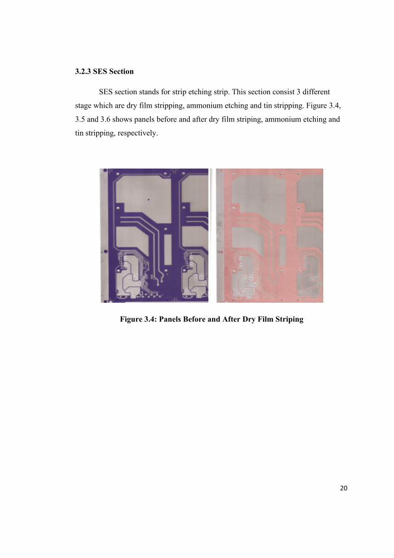
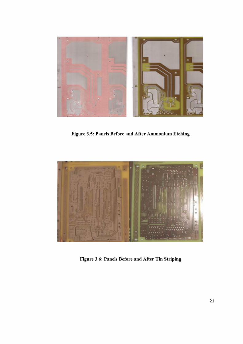
3.2.3 SES Section
SES section stands for strip etching strip. This section consist 3 different
stage which are dry film stripping, ammonium etching and tin stripping. Figure 3.4,
3.5 and 3.6 shows panels before and after dry film striping, ammonium etching and
tin stripping, respectively.
Figure 3.4: Panels Before and After Dry Film Striping
21
Figure 3.5: Panels Before and After Ammonium Etching
Figure 3.6: Panels Before and After Tin Striping
22
3.2.4 Solder mask Pre-treatment and Develop
In solder mask pre-treatment section, panels will be clean from impurities in
microetch G5 tank. Then, panels will be provided with optimum roughness for
excellent ink adhesion in multiprep tank. Besides, anti-tarnish solution is used to
prevent copper surface from oxidation.
After undergo pre-treatment, ink will be printed on the panels before
exposing pattern on its surface. Then, unwanted ink on panels will be removed in
solder mask developing chamber. Final bake is needed in order to cure solder mask
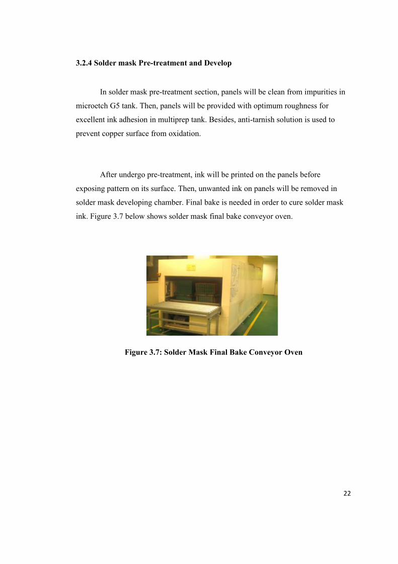
ink. Figure 3.7 below shows solder mask final bake conveyor oven.
Figure 3.7: Solder Mask Final Bake Conveyor Oven
23
3.3 Routine Jobs
3.3.1 Taking Samples
During this industrial training, trainee need to take samples from each section
every morning, afternoon and evening. Normally, sample was collected from on
8:30 am every day. Morning samples are from blackhole, solder mask develop, dry
film and desmear. For normal production schedule, lab section will take samples
from copper plating around 11:30 am. Exception for samples from OSP, HAL, SES
and solder mask pre-treatment (multiprep), each section technician will collect
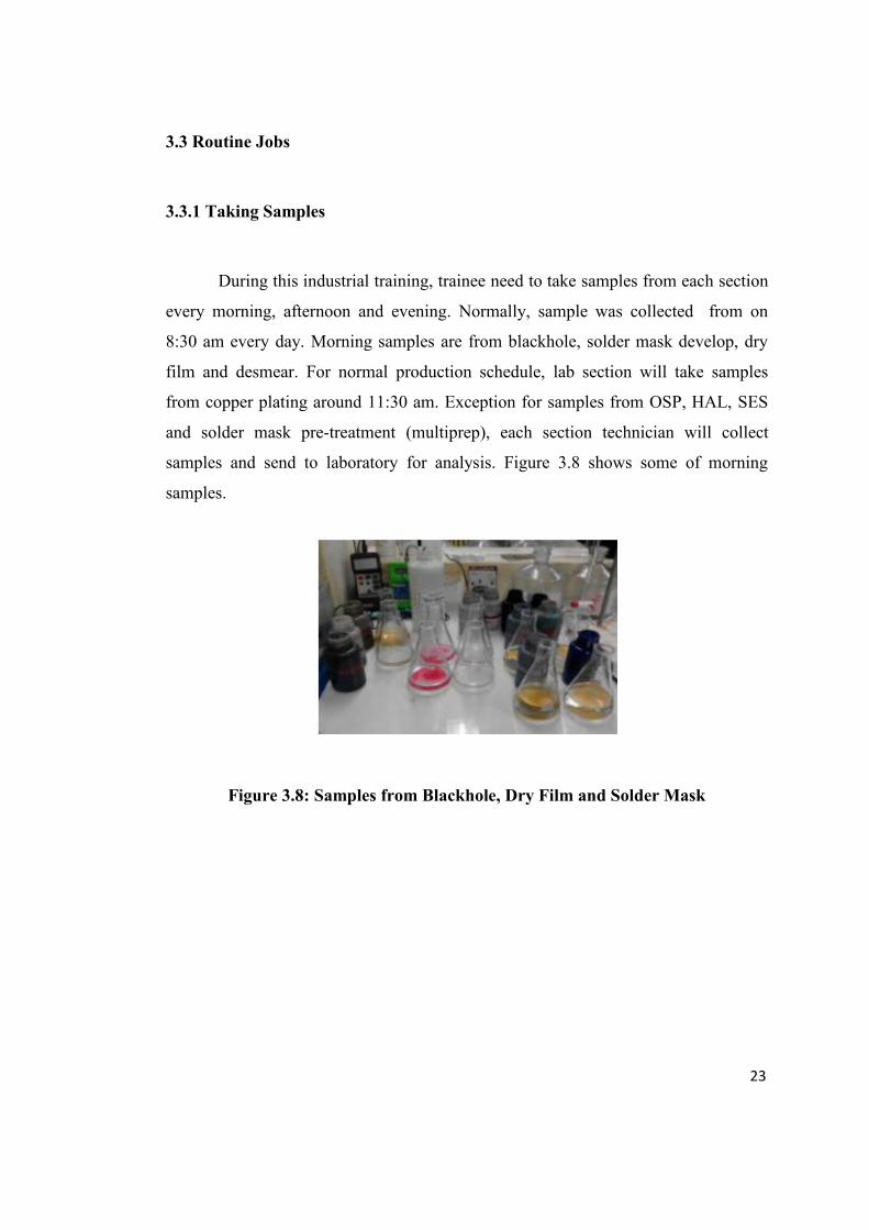
samples and send to laboratory for analysis. Figure 3.8 shows some of morning
samples.
Figure 3.8: Samples from Blackhole, Dry Film and Solder Mask
24
3.3.2 Analysis, Observation and Monitoring Samples
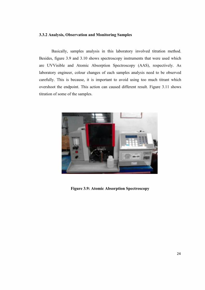
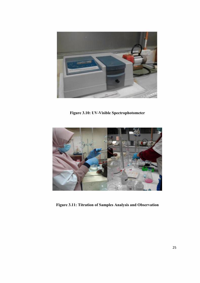
Basically, samples analysis in this laboratory involved titration method.
Besides, figure 3.9 and 3.10 shows spectroscopy instruments that were used which
are UVVisible and Atomic Absorption Spectroscopy (AAS), respectively. As
laboratory engineer, colour changes of each samples analysis need to be observed
carefully. This is because, it is important to avoid using too much titrant which
overshoot the endpoint. This action can caused different result. Figure 3.11 shows
titration of some of the samples.
Figure 3.9: Atomic Absorption Spectroscopy
25
Figure 3.10: UV-Visible Spectrophotometer
Figure 3.11: Titration of Samples Analysis and Observation

26
Monitoring samples is a process which involved follow up samples and
suggesting for new make-up. Besides, we need to monitored that all chemicals
concentration are in it spec. Low concentration and high concentration chemicals can
affect the ongoing panels. For examples, if concentration of tin which is use in
copper plating section as etch resist was too high, thick layer of tin will be plated on
the panels. Hence, it will be hard to remove thick layer of tin in stripping process
later. If tin residue was present in the panels, it may cause other potential failure such
as presence of stain under solder mask and solder mask peel off. Table 3.1 shows
routine schedule of samples analysis and observation that were conducted every day.
This schedule was arranged according to each section control plan.
27
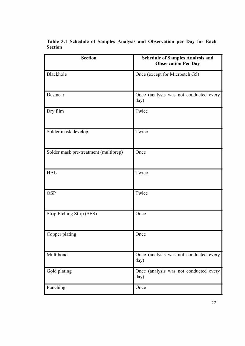
Table 3.1 Schedule of Samples Analysis and Observation per Day for EachSection
Section Schedule of Samples Analysis andObservation Per Day
Blackhole Once (except for Microetch G5)
Desmear Once (analysis was not conducted everyday)
Dry film Twice
Solder mask develop Twice
Solder mask pre-treatment (multiprep) Once
HAL Twice
OSP Twice
Strip Etching Strip (SES) Once
Copper plating Once
Multibond Once (analysis was not conducted everyday)
Gold plating Once (analysis was not conducted everyday)
Punching Once
28
Besides, we need to monitor etching rate and make sure that etching rate is within
specification. High etch rate indicates insufficient copper thickness due to high
concentration of chemicals concentration or high temperature. Thus, from samples
analysis we can decide whether we need to add water, add chemicals or adjust the
temperature.
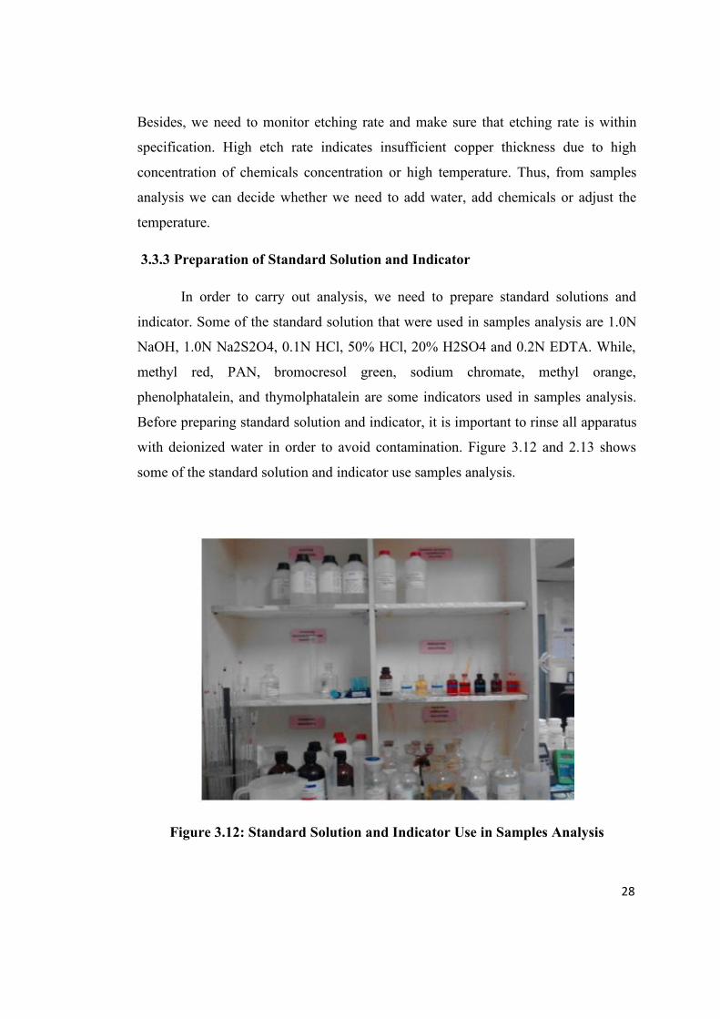
3.3.3 Preparation of Standard Solution and Indicator
In order to carry out analysis, we need to prepare standard solutions and
indicator. Some of the standard solution that were used in samples analysis are 1.0N
NaOH, 1.0N Na2S2O4, 0.1N HCl, 50% HCl, 20% H2SO4 and 0.2N EDTA. While,
methyl red, PAN, bromocresol green, sodium chromate, methyl orange,
phenolphatalein, and thymolphatalein are some indicators used in samples analysis.
Before preparing standard solution and indicator, it is important to rinse all apparatus
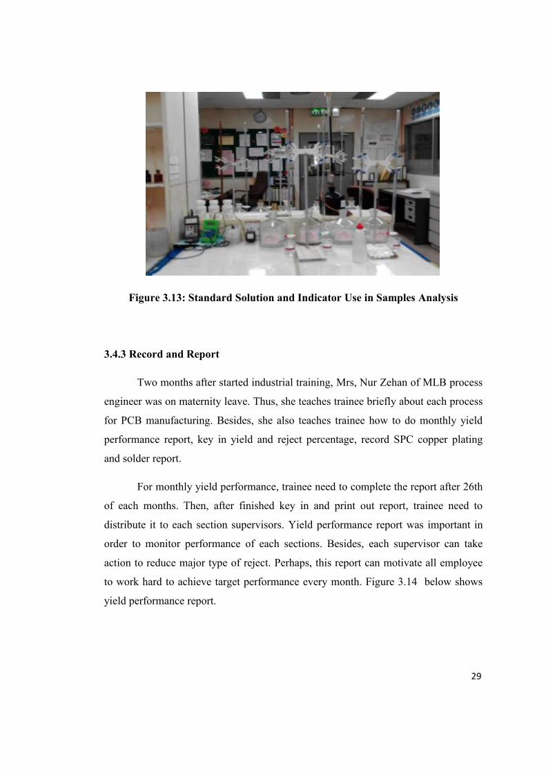
with deionized water in order to avoid contamination. Figure 3.12 and 2.13 shows
some of the standard solution and indicator use samples analysis.
Figure 3.12: Standard Solution and Indicator Use in Samples Analysis
29
Figure 3.13: Standard Solution and Indicator Use in Samples Analysis
3.4.3 Record and Report
Two months after started industrial training, Mrs, Nur Zehan of MLB process
engineer was on maternity leave. Thus, she teaches trainee briefly about each process
for PCB manufacturing. Besides, she also teaches trainee how to do monthly yield
performance report, key in yield and reject percentage, record SPC copper plating
and solder report.
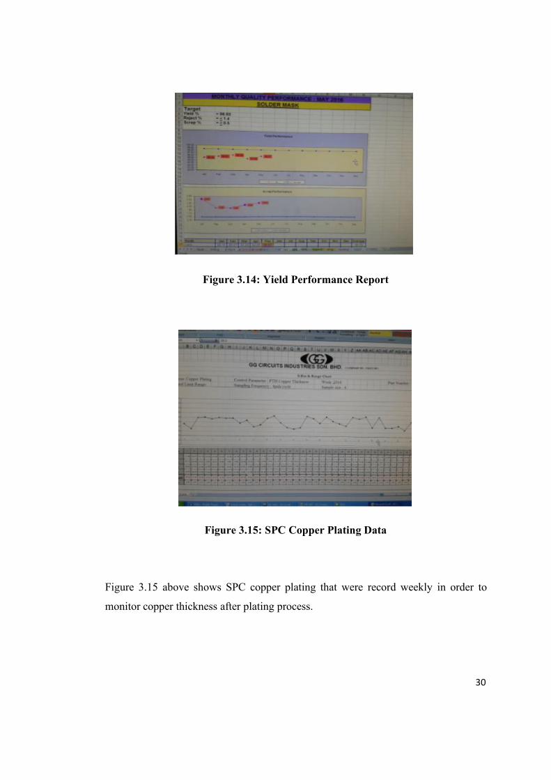
For monthly yield performance, trainee need to complete the report after 26th
of each months. Then, after finished key in and print out report, trainee need to
distribute it to each section supervisors. Yield performance report was important in
order to monitor performance of each sections. Besides, each supervisor can take
action to reduce major type of reject. Perhaps, this report can motivate all employee
to work hard to achieve target performance every month. Figure 3.14 below shows
yield performance report.
30
Figure 3.14: Yield Performance Report
Figure 3.15: SPC Copper Plating Data
Figure 3.15 above shows SPC copper plating that were record weekly in order to
monitor copper thickness after plating process.
31
CHAPTER 4
CONCLUSION AND RECOMMENDATIONS
As conclusion, trainee managed to learn new things within 16 weeks of
industrial training. Besides, trainee was able to build confidence level, teamwork and
good relationships with other employees. Within this training, trainee was able to
expand knowledge and skills on handling chemicals, quality surveyor and others.
Furthermore, exposure of industrial training give student a real working
environment. Besides, throughout this training, trainee learned to practice more
safety precaution in the industry. Industrial training also worked as basic preparation
for working life after graduate.
GGC is a good company for those who wished to experience real working life.
Moreover, GGC also concerned to produce a multi-tasking employee which able to
do various type of job
There are some recommendations that the author would like to suggest to
UniKL MICET for the next coming Industrial Training candidates to gain better
working experience and knowledge. The current months of Industrial Internship
Training Program which is four months are not sufficient enough for the trainee to
gain experience and knowledge. The author would suggest that the duration of
training which is in five to six months should implement so that more experience and
knowledge could be gained. Moreover, Student Industrial Training Unit (INTRA)
needs to prepare a list of companies that are suitable to the student’s respective
course. This is to avoid the student from undergoing training in the company that is
not related to their field of study. Student Industrial Training Unit also needs to
32
provide some general information for each company listed to help student to
understand the host company first before undergo their training there. INTRA also
need to remind the student to seek earlier the place they want to intern as this will
ease the flow for INTRA itself as it can process their form earlier. This also helps the
host company which provide a longer time for them to choose and think about the
intern they want to take. The author also reminds the student in UniKL MICET to
choose the host company based on their field of study, not referring to allowances or
place to intern. This is to prevent the difficulties in performing projects in the host
company if the company working environment is not related to the student’s field of
study. Lastly, creating more working environment activities in UniKL MICET will
helps student to gain experience, practice their work ethics and increase their
professionalism.