Embed Size (px)
Citation preview

Thin Solid Films 551 (2014) 127–130
Contents lists available at ScienceDirect
Thin Solid Films
j ourna l homepage: www.e lsev ie r .com/ locate / ts f
Ferroelectric enhancement of La-doped BaTiO3 thin films using SrTiO3
buffer layer
Ahmed I. Ali a,c, Kibog Park b, Amir Ullah a, Rock Huh c, Y.S. Kim c,d,1
a Basic Science Department, Faculty of Industrial Education, Helwan University, Cairo 11281, Egyptb School of Electrical & Computer Engineering, Ulsan National Institute of Science and Technology, Ulsan 689-798, South Koreac Energy Harvest–Storage Research Center and Department of Physics, University of Ulsan, Ulsan 680-749, South Koread Department of Physics, Applied Physics and Astronomy, Binghamton University, Binghamton, NY 13902, USA
E-mail address: [email protected] (Y.S. Kim).1 Tel.: +82 52 259 2326; fax: +82 52 259 1693.
0040-6090/$ – see front matter © 2013 Elsevier B.V. All rihttp://dx.doi.org/10.1016/j.tsf.2013.11.048
a b s t r a c t
a r t i c l e i n f oArticle history:Received 13 April 2013Received in revised form 7 November 2013Accepted 12 November 2013Available online 20 November 2013
Keywords:PolarizationFerroelectricSrTiO3buffer layerLa-doped BaTiO thin film3
Pulsed laser deposition
Pulsed laser deposition (PLD) was used to fabricate La0.01Ba0.99TiO3 (LBTO) thin films on MgO/TiO2/SiO2/Sisubstrates with and without SrTiO3 (STO) buffer layer. LBTO films deposited on STO layers exhibited enhancedferroelectricity and decreased leakage current (9 × 10⁻⁷ A/cm2 at 50 kV/cm), conductivity, and Hall mobility,compared to those of LBTO films on MgO substrate. The remanent polarization (Pr) and coercive field (Ec) forLBTO thin films on STO bufferedMgO substrate dramatically improved, 36.5 μC/cm2 and ~220 kV/cm, comparedto those for LBTO thin films on MgO substrate, 3 μC/cm2 and ~60 kV/cm. The degradation of Pr and Ec after 105
switching test is less than 0.1% for LBTO thin films on STO buffered MgO substrate. This work demonstrates aroute to a lead-free ferroelectric thin film for nonvolatile memories and electro-optic devices.
© 2013 Elsevier B.V. All rights reserved.
1. Introduction
In recent years, ferroelectric thin films have exhibited potential inmany important applications, including non-volatile ferroelectric ran-dom access memories (FeRAM) and infrared sensors. Ferroelectric ma-terials suitable for these applications include Pb(Zr,Ti)O3, SrBi2Ta2O9,Bi4Ti3O12 and BaTiO3 (BTO) systems, which have been studied exten-sively. BaTiO3 has several advantages such as an extremely low coercivefield, high remanent polarization, mechanical strength, and small devi-ation in composition. So BTO have a strong potential for application inferroelectric thin film devices [1]. In addition, strip-loaded type opticalwaveguide structures based on BTO thin film technology with promis-ing electro-optic response have been reported [2]. Moreover, thesestructures are likely to achieve high levels of component integration inmicro-photonic applications, including light sources, modulators,wave-guides, and detectors with reduced device size [3].
Doping ceramic with rare earth elements is an effective method foroptimizing the dielectric and ferroelectric properties [4]. BaTiO3 dopedwith La couldmodifyfilmproperties, semiconducting states and crystal-line phase orientation (paraelectric or ferroelectric phase) dependingon doping type. A-site doping of BTO with La3+ gives both a high
ghts reserved.
dielectric constant and Curie temperature (Tc) [5–7]. The reduction oflattice mismatch between perovskite films and substrates depends onthe type and orientation of the substrate [8].
The ferroelectric properties of La0.01Ba0.99TiO3 (LBTO) thin film canbe enhanced for FeRAM applications by selecting proper depositionconditions [4] and methods [2,4,9–11], doping type and doping level[5–7,12–15], and substrates [16].MgO is a suitablematerial for use in in-tegrated optics because it can be an integral part of a waveguide device,while allowing growth of high quality La0.01Ba0.99TiO3 thin films. Thereare several reasons to select the MgO film as substrate. First, its latticeparameter (ao = 4.213 Å) is reasonably close to those of tetragonalLBTO (a = 3.994 Å, c = 4.038 Å) at room temperature. Second, its re-fractive index (n = 1.7 at 0.6 μm) is much lower than that of BTO(n = 2.4 at 0.6 μm), which facilitates wave guiding in thin BTO films.Third, MgO does not exhibit a linear electro-optic effect [8]. Since MgOfilms has a lower refractive index than BTO and smaller optical loss,we expect LBTO films to be similar to BTO films because of the low dop-ing level of La element in BTO (1 mol%). The use ofMgO as a buffer layeralso reduces inter-diffusion and oxidation problems, which are preva-lent for these semiconductor substrates. Since, MgO is a semiconductorand La3+ in LBTO can increase leakage current, it is necessary to insertthe STO film between LBTO and MgO films as a buffering dielectriclayer to increase the dipole moment between La3+ and Sr2+ ions. Onthese basis, the increase of ferroelectricity and decrease of current den-sity with the LBTO films deposited on the STO buffered MgO substratecan be expected.

Table 1Electrical properties measured by Hall measurements system at room temperature ofLa0.01Ba0.99TiO3 thin films grown on MgO and STO-layer/MgO substrates using pulsedlaser deposition.
Sample Resistivity(Ω · m)
Carrier mobility(cm2/V · s)
Carrier concentration(#/cm3)
LBTO/MgO 6.52 × 10⁴ 2.34 × 10³ (n-type) 7.27 × 10¹¹
LBTO/STO-layer 8.12 × 10⁶ 41.1 (n-type) 7.09 × 10⁸
128 A.I. Ali et al. / Thin Solid Films 551 (2014) 127–130
Pulsed laser deposition (PLD)was used to fabricate thin La0.01Ba0.99TiO3
(LBTO) films on both MgO/TiO2/SiO2/Si (MgO) and SrTiO3-layer/MgO/TiO2/SiO2/Si (STO-layer/MgO) substrates. The film structure was char-acterized using X-ray diffraction (XRD) and field emission secondaryelectron microscopy (FE-SEM). In addition, ferroelectricity and electri-cal properties were also investigated.
2. Experiments
SrTiO3 and Ba0.99La0.01TiO3 bulk ceramic targets were prepared by aconventional powder processing unit. High purity powders of SrCO3
(99.99%), TiO2 (99.99%), BaCO3 (99.9%), and La2O3 (99.99%), were pur-chased from Sigma-Aldrich. The powders were intimately mixed in anethanol medium with zirconia balls by stirring in a high-speed turbineat 6000 rpm for 24 h. The slurry was dried at 100 °C. Mixtures werecrushed into powdered form, ground lightly in an agate mortar, andsieved through a 100 μm mesh screen. The obtained powder was firedat 1200 °C under atmospheric environments for 5 h. This process wasrepeated, and the powder was then molded into a pellet (ca. 1.2 cmradius and 4–5.5 mm thickness) under uni-axial pressure of 15 MPa.This was followed by cold-isostatic pressing under 150 MPa for 20 min.Finally, both STO and LBTO ceramic targets were sintered at 1350 °Cin air for 48 h with heating/cooling rates of 5 °C/min. Target structureswere investigated to confirm the sample phases. X-ray powder diffrac-tion was performed using a Rigaku Co-Miniflex X-ray diffractometeremploying CuKα radiation with λ = 1.5418 Å.
LBTO thin filmswere deposited in two steps. Firstly, PLDwas used tofabricate the SrTiO3 buffer layer onMgO substrates using a SrTiO3 target.Secondly, LBTO thin filmswere deposited on both of STO-layer andMgOsubstrates by PLDusing a KrF laser (Coherent COMPexPro 102F) operat-ing at a wavelength of 248 nm. All films were grown with a repetitionrate of 5 Hz, fluency of 2.0 J/cm2, distance between target and substrateof ~4 cm, substrate temperature of 700 °C, and oxygen partial pressureof 13.3 Pa. After growth, the films were kept in the same gas pressureand substrate temperature for additional annealing for 30 min [17].They were then freely cooled to room temperature for re-oxidization.
Crystal structure analysis of the thin films was carried out by XRDmeasurements. The lattice parameters were calculated from θ–2θ pat-terns (Rigagu RU 300). The thickness and surface morphology of thethin films were observed by using FE-SEM. The thickness of LBTO thinfilm measured by a cross-sectional view of FE-SEM were about 300
a b
Fig. 1. (a) Schemes of La0.01Ba0.99TiO3 thin films grown onMgO/TiO2/SiO2/Si and SrTiO3-layer/Mthin films grown on MgO and STO buffered MgO substrates by pulsed laser deposition.
(deposition rate = 3.3 nm/min) and 500 nm (deposition rate =5.3 nm/min) for MgO and STO-layer substrates, respectively. Thedeposited STO film showed about 150 nm thick (deposition rate =2.2 nm/min). RF magnetron sputtering was used to fabricate Pt topelectrodes in the form of 100 μm disks and 100 nm thicknesses onLBTO films. After deposition of the top electrodes, films were annealedat 400 °C for 5 min prior to obtaining ferroelectric hysteresis loops,which were measured using an RT66A (Radiant Technologies, Inc.)test system. Leakage current was measured by a Keithley 2636ASourceMeter. The electrical properties of LBTO thin films were mea-sured using the Hall measurements system at room temperature.
3. Results and discussion
Fig. 1(a) presents the scheme of the LBTO thin films deposited onbothMgO and STO buffered substrates by PLD. The structural propertiesof LBTO thin films onMgO and STO-layerwere analyzed by XRD and arepresented in the upper panel of Fig. 1(b). The pattern contains onlypeaks corresponding to the (111) reflection of LBTO and the (211) re-flection of MgO, demonstrating that the film was highly oriented onthe semiconductor MgO substrate. The average parameter calculatedfrom the 2θ value for three LBTO peaks was 4.001 ± 0.001 Å, whichagrees with the published value of a = 3.994 Å for tetragonal BTO.This indicates that the film was highly oriented on the c-axis normalon the substrate plane. The lower panel of Fig. 1(b) shows the patternof films on insulator STO-layer/MgO, which exhibited random orienta-tion polycrystalline with 6 peaks of LBTO and 3 peaks related to STO-layer andMgO substrate. All peaks were indexedwith the BaTiO3 struc-turewithout any impurity in the interface betweenfilms and substrates.The average lattice parameter calculated from the 2θ value for LBTO
(degree)
gO/TiO2/SiO2/Si substrates by pulsed laser deposition. (b) XRD pattern of La0.01Ba0.99TiO3
a b
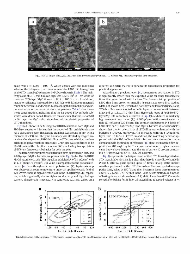
Fig. 2. FE-SEM images of La0.01Ba0.99TiO3 thin films grown on (a) MgO and (b) STO buffered MgO substrates by pulsed laser deposition.
129A.I. Ali et al. / Thin Solid Films 551 (2014) 127–130
peaks was a = 3.992 ± 0.001 Å, which agrees with the publishedvalue for the tetragonal. Hall measurements for LBTO thin films grownon the STO-layer/MgO substrates by PLDare shown in Table 1. The resis-tivity value of LBTO thin films onMgOwas 6.52 × 10⁴ Ω · cmwhile forthose on STO-layer/MgO it was to 8.12 × 10⁶ Ω · cm. In addition,magneto-resistance increased from 5.87 kΩ to 68 kΩ due to magneticcoupling between La and Sr ions. Moreover, both Hall mobility and car-rier concentration decreased at room temperature. Table 1 also showssheet concentration, indicating that the La-doped BTO on both sub-strates were donor doped. Hence, we can conclude that the use of STObuffer layer on MgO substrate enhanced the electric properties ofLBTO thin films.
Fig. 2(a,b) shows FE-SEM images of LBTO thinfilms on bothMgOandSTO-layer substrate. It is clear that the deposited film onMgO substratehas a crystalline phase. The average grain sizewas around 45 nmwith athickness of ~350 nm. The grain boundary was affected by oxygen an-nealing after deposition. LBTO thin films on STO-layer exhibited randomorientation polycrystalline structures. Grain size was confirmed to be50–60 nm and the film thickness was 560 nm, leading to expectationof different ferroelectric behavior for both samples.
The ferroelectric properties of LBTO thin films deposited onMgO andSrTiO3-layer/MgO substrates are presented in Fig. 3(a,b). The Pt/LBTO/MgO/bottom electrode (BE) capacitor exhibited Pr of 3.8 μC/cm2 withan Ec of about 75 kV/cm2. Our value is comparable to the previous re-ported [4]. Even though a saturated polarization (Ps) hysteresis loopwas observed at room temperature under an applied electric field of120 kV/cm, there is high dielectric loss in the Pt/LBTO/MgO/BE capaci-tor, which is generally due to higher conductivity and high leakagecurrent. Therefore, it is necessary to synthesize La0.01Ba0.99TiO3 on a
Fig. 3. Polarization-field dependence (P–E) hysteresis loops of La0.01Ba0.99TiO3 thin films gro
different dielectric matrix to enhance its ferroelectric properties forpractical application.
According to a previous report [4], spontaneous polarization in BTOis significantly lower than the expected value for other ferroelectricfilms that were doped with La ions. The ferroelectric properties ofLBTO thin films grown on metallic Pt-substrates were first studied(data not shown here), which did not show any ferroelectricity. Next,STO thin films were adopted as buffer layer to prevent misfit betweenMgO and La0.01Ba0.99TiO3thin films. Hysteresis loops of Pt/LBTO/STO-layer/MgO/BE capacitors, as shown in Fig. 3(b) exhibited remarkablyhigh remanent polarization (Pr) of 36.5 μC/cm2 with a coercive electricfield (Ec) of about 220 kV/cm. The comparison between P–E loops ofLBTOfilms on STO bufferedMgO andMgO substrates at saturationfieldsshows that the ferroelectricity of LBTO films was enhanced with thebuffered STO layer. Moreover, Pr is increased with the STO bufferedlayer from 3.8 to 36.5 μC/cm2. In addition, the switching behavior ap-peared with the STO buffered MgO substrate. Here the results can becompared with the finding of reference [16] about the BTO thin film de-posited on STO single crystal. Their polarization value is higher than ourvalue but we have demonstrated the use of current IC process compat-ible STO layer over MgO/TiO2/SiO2/Si substrate.
Fig. 4(a) presents the fatigue result of the LBTO films deposited onSTO-layer/MgO substrate. It is clear that there is a very little change inPr and Ec after AC pulse cycling up to 105 times. Finally, static imprintwas then performed on the LBTO films where filmswere poled into op-posite state, baked at 150 °C and then hysteresis loops were measuredafter 1, 5, 24 and 36 h. The shift in the Pr and Ec was plotted as a functionof baking time (not shown here). A Ec shift of less than 0.25 V was ob-served after baking for 36 h for all tested films at applied voltage 18 V.
wn on (a) MgO and (b) STO buffered MgO substrates measured at room temperature.

Fig. 4. (a) Fatigue results of remnant polarization (Pr) and conceive field (Ec) up to 105 cycle time. (b) Leakage current density as a function of applied field of La0.01Ba0.99TiO3 thin filmsgrown on MgO and STO buffered MgO substrates measured at room temperature.
130 A.I. Ali et al. / Thin Solid Films 551 (2014) 127–130
Extrapolating the plotted Ec values for a longer time, indicated there isno imprint failure in Ec or Pr with the time. The results indicated thatthe LBTO film imprint in the capacitors was independent of the mea-surement time.
Fig. 4(b) shows the leakage current density curves of Pt/LBTO/MgO/BE and Pt/LBTO/STO-layer/MgO/BE capacitor as a function of appliedfield. Current density for the Pt/LBTO/STO-layer/MgO/BE capacitor(9 × 10⁻⁷ A/cm2 at maximum electric fields of 50 kV) decreasedmore than that of the Pt/LBTO/MgO/BE capacitor (8 × 10⁻⁶ A/cm2 atmaximumelectricfields of 8 kV). The relation between J and E for differ-ent electric field is J = cEn. The exponent can vary from 0 b n ≤ ∞. Theconduction mechanism for LBTO on both MgO and STO-layer/MgOsubstrate can be divided into two regions. At lower electric fields, bothfilms showed current density that increased slightly with applied elec-tric field by an Ohmic conductionmechanism (n b 1). At higher appliedfield regions, the values of n were higher than 3. For distribution trapspace charge conduction, n can be from 2 to ~12. Space-charge-limitedconduction was due to electrons or holes ejected from electrodes intothe dielectric sample. The value of n for thin films deposited on MgOand STO-layer were ~11.23 and 57.18, respectively. This indicates thatthe film on MgO has higher charge carrier density than the film on theSTO-layer. Therefore, leakage current on the STO-layer is adjustedwith the STO-layer. This suggests that the film improved in qualityand the interface properties between the Ba0.99La0.01TiO3 thin film andthe SrTiO3 substratewere better than those between theBa0.99La0.01TiO3
thin film and the MgO substrate.Our data confirmed that A-site doping of ferroelectric perovskite
was enhanced with the STO buffer layer. In addition, it decreased leak-age current density by around 8%. We suggest that enhanced Pr of theLBTO thin film is due to the strain between the film and the SrTiO3
layer. The experimental results of spontaneous polarization suggeststudy of the first-principles of LBTO, which may determine the reasonfor large polarization value. The remanent polarization of LBTO thinfilm was 38 μC/cm2, which is appropriate for FeRAM applications.LBTO film is lead free ferroelectric (no toxicity or volatility of the leadand bismuth), and low cost, which makes it a good candidate for moreapplications in industry. We suggest the use of the STO layer withLBTO thin films rather than the MgO wafer substrate and/or Pb(Zr,Ti)O3 and SrBi2Ta2O9. Finally, we demonstrated that the ferroelectric prop-erties of LaBaTiO3 can be enhanced with the use of SrTiO3-layer for fer-roelectric memory applications.
4. Conclusion
We used PLD method to fabricate thin films of La0.01Ba0.99TiO3onMgO/TiO2/SiO2/Si (MgO) and SrTiO3/MgO/TiO2/SiO2/Si (STO-layer)
substrates. The films were well oriented on MgO substrate, and poly-crystalline on STO-layer substrate. FE-SEM was used to examine thethickness and the surface of La0.01Ba0.99TiO3films. Electrical data re-vealed insulating and semiconducting behavior for thin films depositedon the STO-buffered MgO substrate and MgO substrates, respective-ly. In addition, the inserting of the STO-layer with the films decreasedboth conductivity, mobility, and the leakage current. The P–E loopsshowed the dramatic enhancement of saturation polarization valuesof 36.5 μC/cm2 at 220 kV/cm and about 4 μC/cm2 at 75 kV/cm2 forLa0.1Ba0.99TiO3 thin films on STO buffered MgO substrate and Mg sub-strate, respectively. The degradation of Pr and Ec after 105 cycling testis less than 0.1% for LBTO thin films on STO-buffered MgO substrate.This work demonstrates a route to a lead-free ferroelectric thin filmfor nonvolatile memories and electro-optics devices.
Acknowledgment
This research was supported by the Basic Science Research Program(Grant No. 2012-1010369) and Priority Research Centers Program(Grant No. 2009-0093818) through the National Research Foundation ofKorea (NRF) funded by the Ministry of Education.
References
[1] B.H. Hoerman, G.M. Ford, L.D. Kaufmann, B.W. Wessels, Appl. Phys. Lett. 73 (1998)2248.
[2] S. Kim, T. Fujimoto, T. Manabe, I. Yamaguchi, T. Kumagai, S. Mizuta, J. Mater. Res. 14(1999) 592.
[3] H.B. Sharma, H.N.K. Sarma, A. Mansingh, J. Appl. Phys. 85 (1999) 341.[4] S.M. Bobade, D.D. Gulwade, A.R. Kulkarni, P. Gopalan, J. Appl. Phys. 97 (2005)
074105(7 pages).[5] O.D. Jayakumar, S.N. Achary, K.G. Girija, A.K. Tyagi, C. Sudakar, G. Lawes, R. Naik, J.
Nisar, X. Peng, R. Ahuja, Appl. Phys. Lett. 96 (2010) 032903(3 pages).[6] Z.X. Cheng, X.L. Wang, S.X. Dou, H. Kimura, K. Ozawa, J. Appl. Phys. 104 (2008)
116109(3 pages).[7] D.B. Buchholz, R.P.H. Chan, J.-Y. Song, J.B. Ketterson, Appl. Phys. Lett. 87 (2005)
082504(3 pages).[8] H.L. Ju, C. Eylem, J.L. Peng, B.W. Eichhorn, R.L. Greene, Phys. Rev. B 49 (1994) 13335.[9] J. Yao, C. Xiong, L. Dong, C. Chen, Y. Lei, L. Chen, R. Li, Q. Zhu, X. Liu, J. Math. Chem. 19
(2009) 2817.[10] L.A. Wills, B.W. Wessels, D.S. Richeson, T.J. Marks, Appl. Phys. Lett. 60 (1992) 41.[11] T. Hayashi, N. Oji, H. Maiwa, Jpn. J. Appl. Phys. 33 (1994) 5277.[12] J. Xu, G. Wang, H. Wang, D. Ding, Y. He, Mater. Lett. 63 (2009) 855.[13] B. Xu, K.B. Yin, J. Lin, Y.D. Xia, X.G. Wan, J. Yin, X.J. Bai, J. Du, Z.G. Liu, Phys. Rev. B 79
(2009) 134109(5 pages).[14] Y.-H. Lin, J. Yuan, S. Zhang, Y. Zhang, J. Liu, Y. Wang, C.-W. Nan, Appl. Phys. Lett. 95
(2009) 033105(3 pages).[15] J.M.D. Coey, M. Venkatesan, C.B. Fitzgerald, Nat. Mater. 4 (2005) 173.[16] K.J. Choi, M. Biegalski, Y.L. Li, A. Sharan, J. Schubert, R. Uecker, P. Reiche, Y.B.
Chen, X.Q. Pan, V. Gopalan, L.-Q. Chen, D.G. Schlom, C.B. Eom, Science 306(2004) 1005.
[17] M. Cernea, J. Optoelectron. Adv. Mater. 6 (2004) 1349.

![Study on the Thermoelectric Properties of SrTiO3-SrNbO3 ...1. General Introduction 2 for electronic refrigerators [Fig. 1.1(b)]. Pielter effect could be quantified by the Pielter coefficient,](https://img.pdfslide.tips/doc/110x75/60e94f2f032c0a4ef7200fe1/study-on-the-thermoelectric-properties-of-srtio3-srnbo3-1-general-introduction.jpg)