Embed Size (px)
Citation preview
ლექცია I
ნახშირბადის ნანოტექნოლოგია
prof. aleqsandre Sengelaia
ivane javaxiSvilis sax. Tbilisis
saxelmwifo universiteti
Copyright©2000 by Houghton
Mifflin Company. All rights
reserved.
2
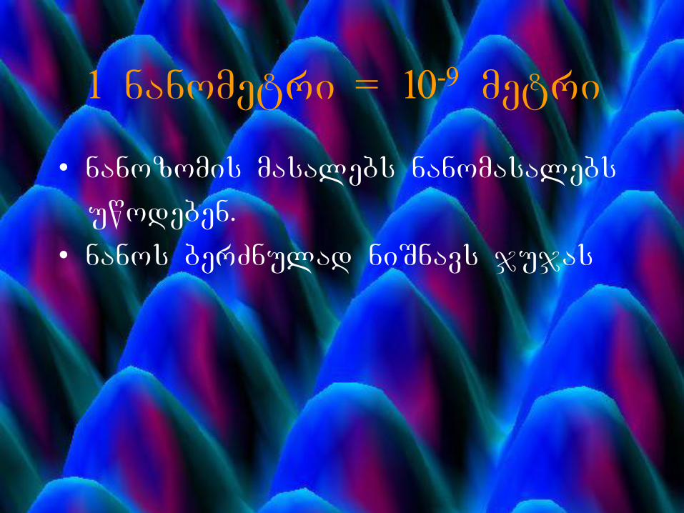
1 nanometri = 10-9 metri
• nanozomis masalebs nanomasalebs
uwodeben.
• nanos berZnulad niSnavs jujas
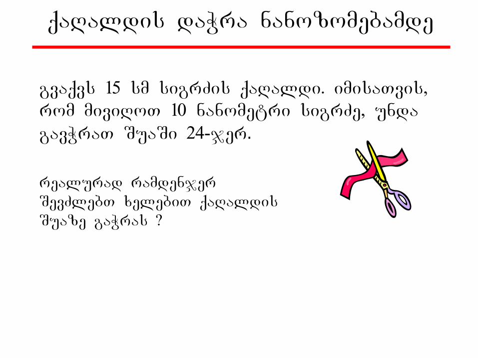
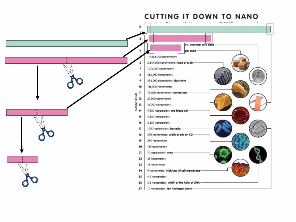
qaRaldis daWra nanozomebamde
gvaqvs 15 sm sigrZis qaRaldi. imisaTvis, rom miviRoT 10 nanometri sigrZe, unda gavWraT SuaSi 24-jer.
realurad ramdenjer SevZlebT xelebiT qaRaldis Suaze gaWras ?
5
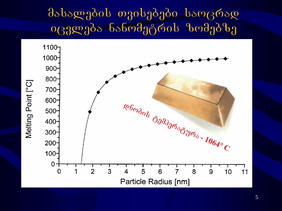
masalebis Tvisebebi saocrad icvleba nanometris zomebze
6
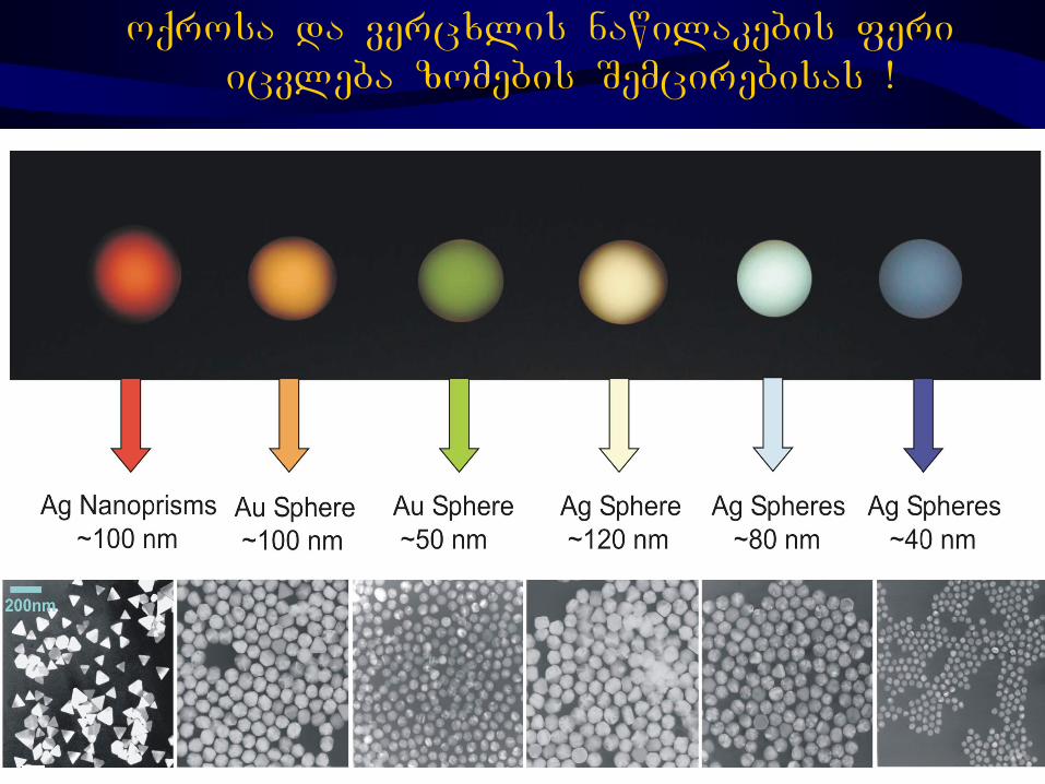
oqrosa da vercxlis nawilakebis feri icvleba zomebis Semcirebisas !
7
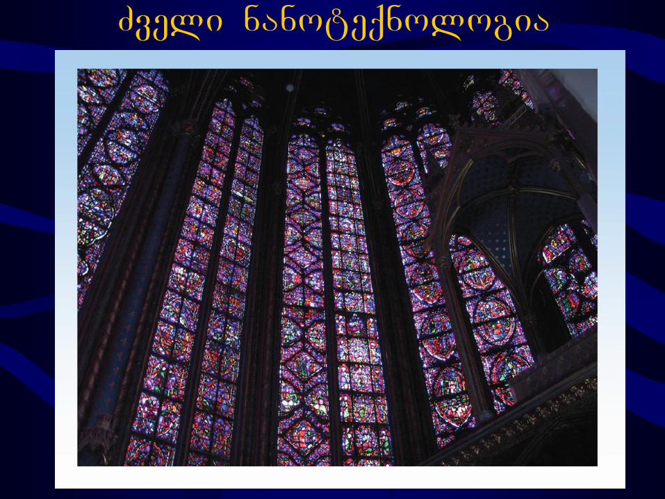
Zveli nanoteqnologia
8
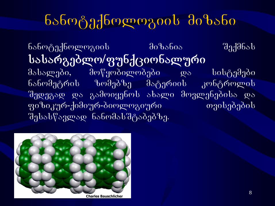
nanoteqnologiis mizani
nanoteqnologiis mizania Seqmnas
sasargeblo/funqcionaluri masalebi, mowyobilobebi da sistemebi nanometris zomebze materiis kontrolis Sedegad da gamoiyenos axali movlenebisa da fizikur-qimiur-biologiuri Tvisebebis Sesaswavlad nanomasStabebze.
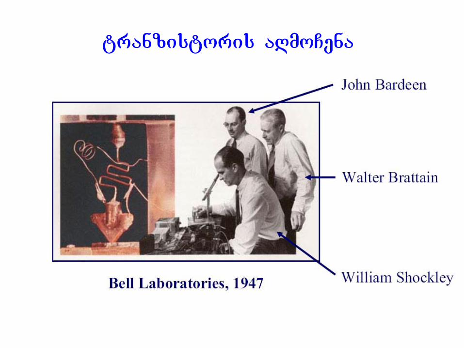
tranzistoris aRmoCena
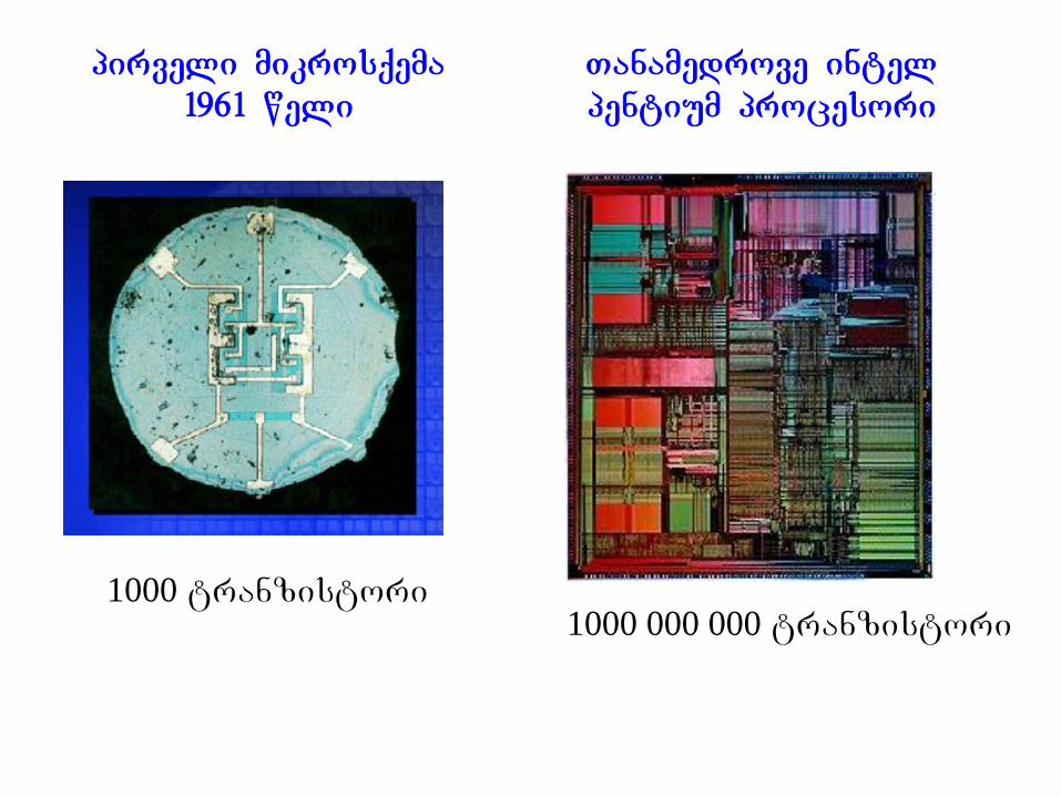
pirveli mikrosqema 1961 weli
Tanamedrove intel pentium procesori
1000 000 000 tranzistori 1000 tranzistori
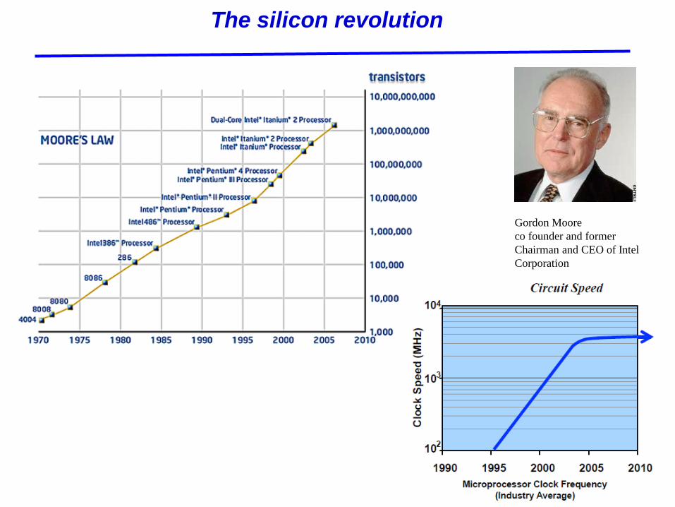
The silicon revolution
Gordon Moore
co founder and former
Chairman and CEO of Intel
Corporation
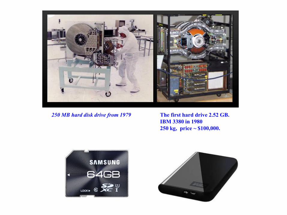
250 MB hard disk drive from 1979 The first hard drive 2.52 GB.
IBM 3380 in 1980
250 kg, price ~ $100,000.
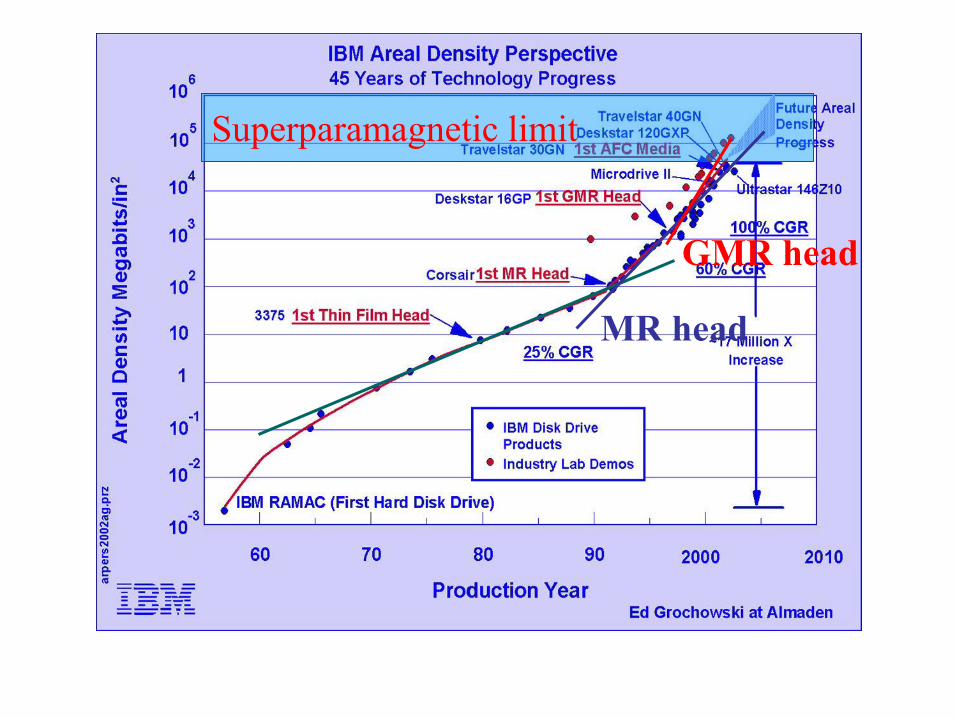
Superparamagnetic limit
MR head
GMR head
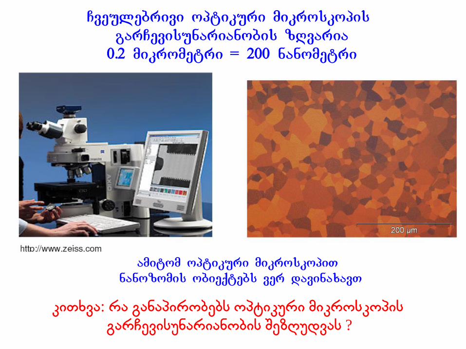
Cveulebrivi optikuri mikroskopis garCevisunarianobis zRvaria
0.2 mikrometri = 200 nanometri
amitom optikuri mikroskopiT nanozomis obieqtebs ver davinaxavT
კითხვა: რა განაპირობებს ოპტიკური მიკროსკოპის
გარჩევისუნარიანობის შეზღუდვას ?
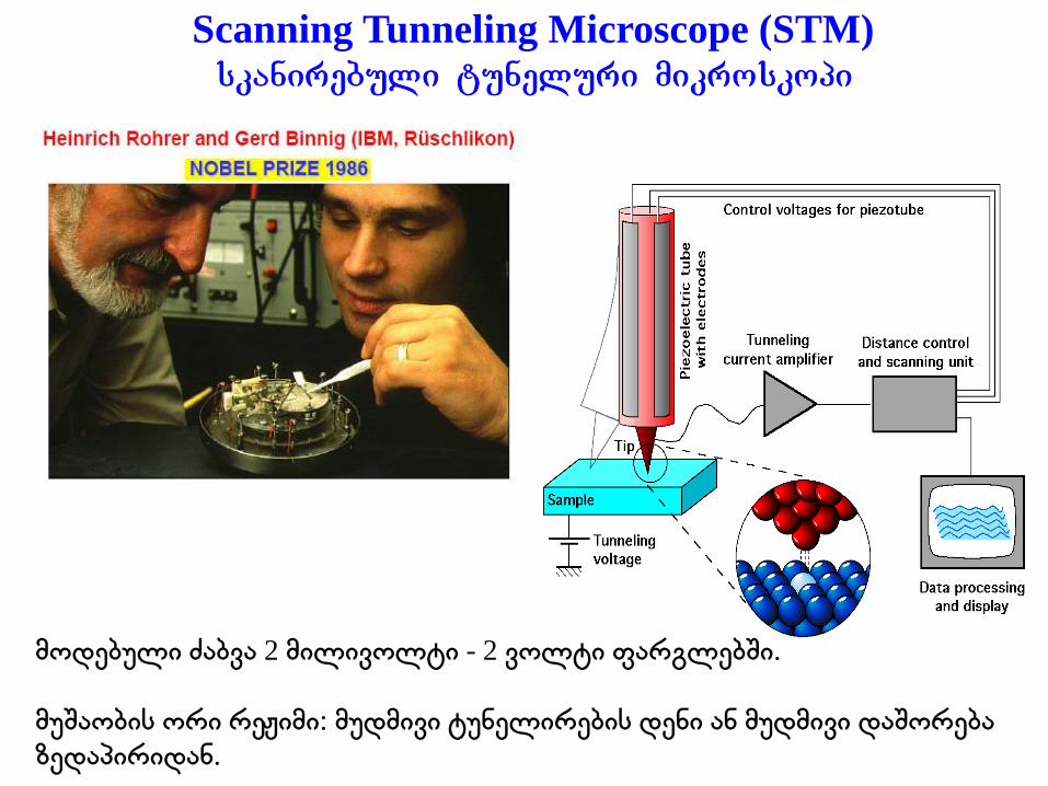
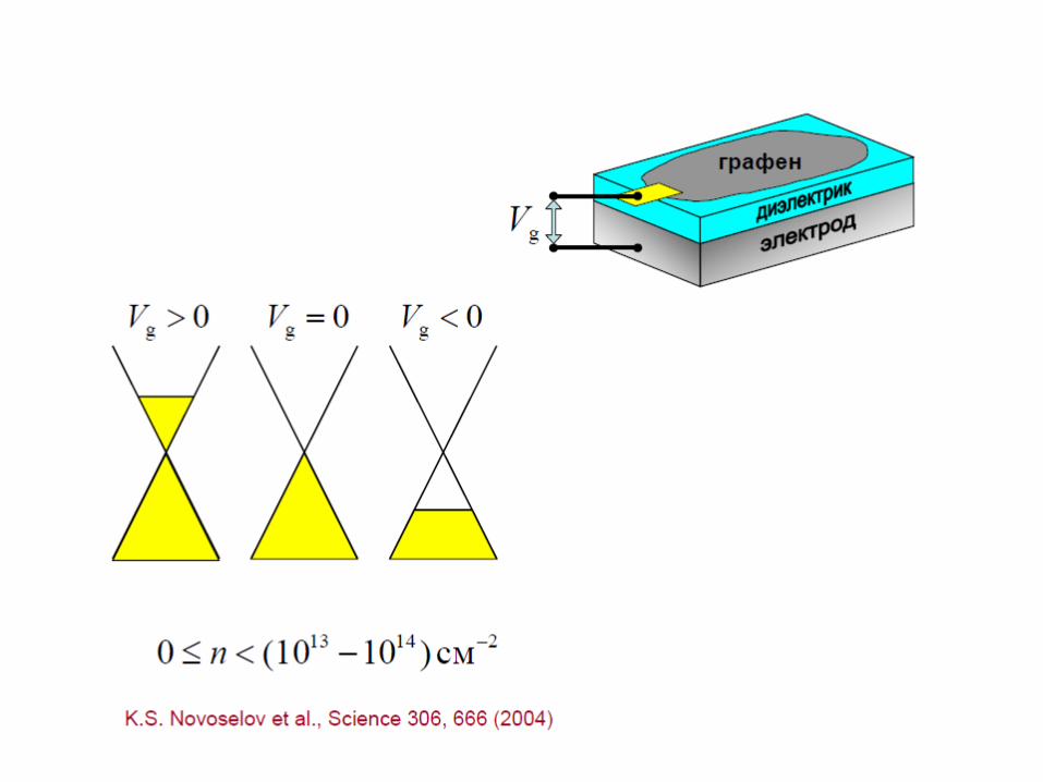
Scanning Tunneling Microscope (STM) skanirebuli tuneluri mikroskopi
მოდებული ძაბვა 2 მილივოლტი - 2 ვოლტი ფარგლებში.
მუშაობის ორი რეჟიმი: მუდმივი ტუნელირების დენი ან მუდმივი დაშორება
ზედაპირიდან.
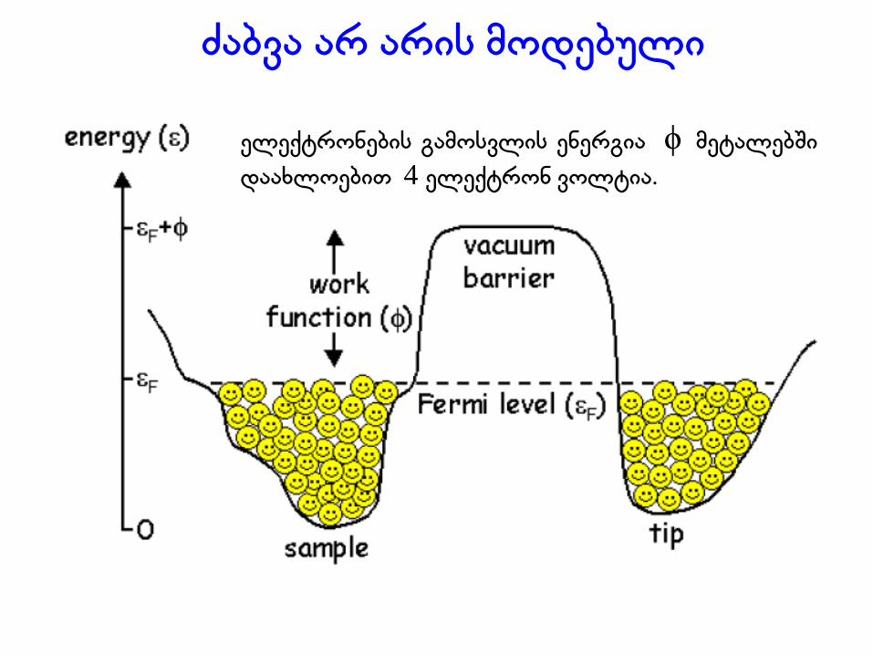
ძაბვა არ არის მოდებული
ელექტრონების გამოსვლის ენერგია ϕ მეტალებში
დაახლოებით 4 ელექტრონ ვოლტია.
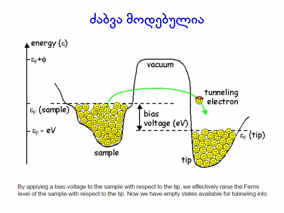
ძაბვა მოდებულია
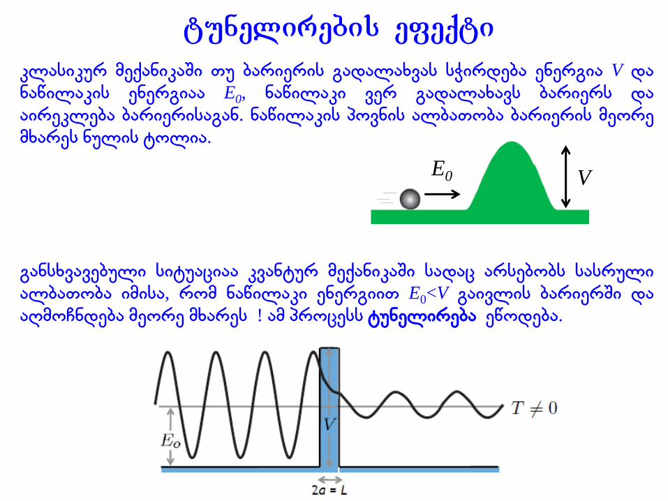
tunelirebis efeqti
კლასიკურ მექანიკაში თუ ბარიერის გადალახვას სჭირდება ენერგია V და
ნაწილაკის ენერგიაა E0, ნაწილაკი ვერ გადალახავს ბარიერს და
აირეკლება ბარიერისაგან. ნაწილაკის პოვნის ალბათობა ბარიერის მეორე
მხარეს ნულის ტოლია.
განსხვავებული სიტუაციაა კვანტურ მექანიკაში სადაც არსებობს სასრული
ალბათობა იმისა, რომ ნაწილაკი ენერგიით E0<V გაივლის ბარიერში და
აღმოჩნდება მეორე მხარეს ! ამ პროცესს ტუნელირება ეწოდება.
V E0
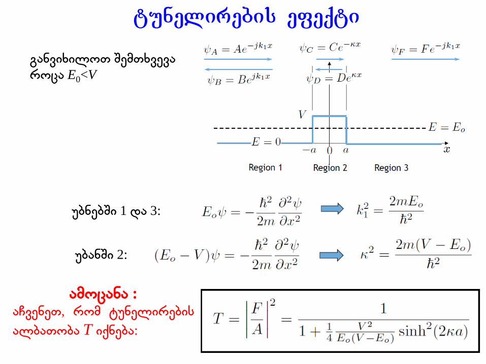
tunelirebis efeqti
განვიხილოთ შემთხვევა
როცა E0<V
უბნებში 1 და 3:
უბანში 2:
ამოცანა : აჩვენეთ, რომ ტუნელირების
ალბათობა T იქნება:
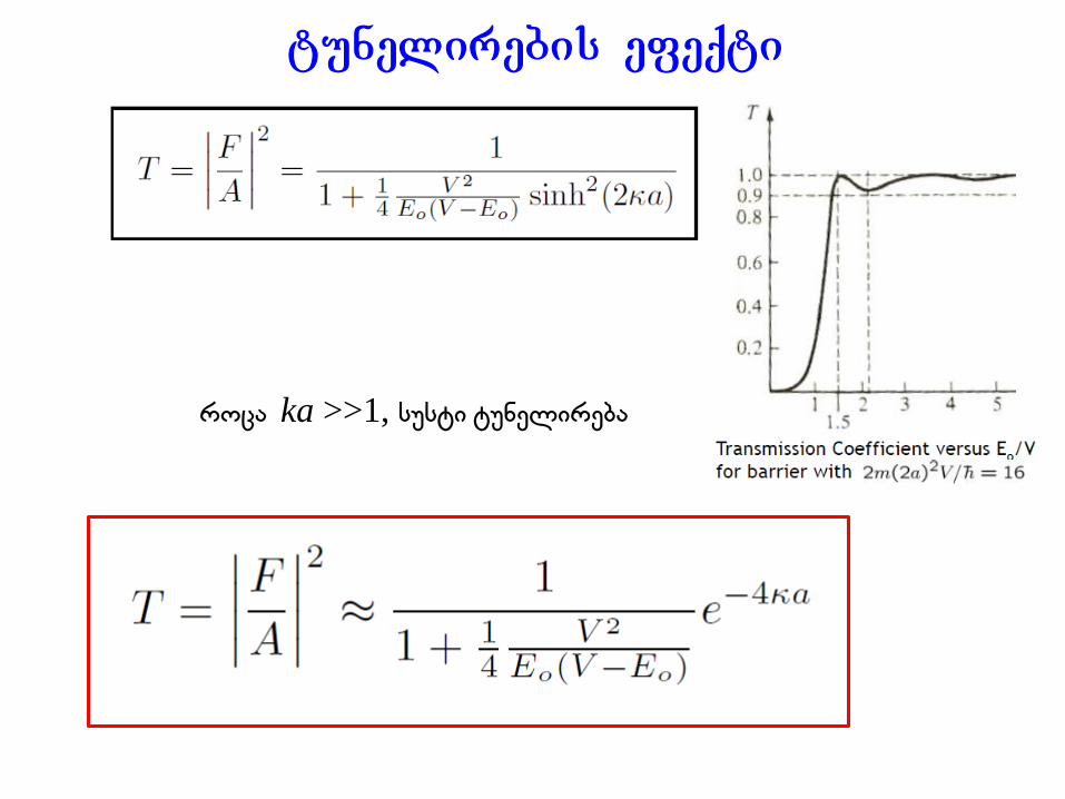
tunelirebis efeqti
როცა ka >>1, სუსტი ტუნელირება
tunelirebis efeqti
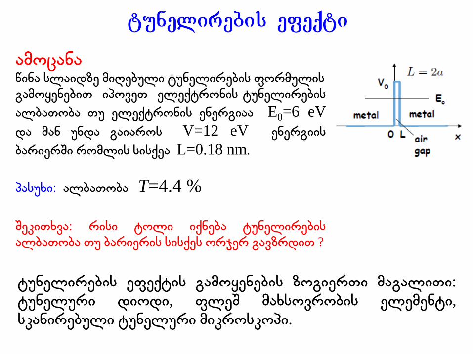
ამოცანა წინა სლაიდზე მიღებული ტუნელირების ფორმულის
გამოყენებით იპოვეთ ელექტრონის ტუნელირების
ალბათობა თუ ელექტრონის ენერგიაა E0=6 eV
და მან უნდა გაიაროს V=12 eV ენერგიის
ბარიერში რომლის სისქეა L=0.18 nm.
პასუხი: ალბათობა T=4.4 %
შეკითხვა: რისი ტოლი იქნება ტუნელირების
ალბათობა თუ ბარიერის სისქეს ორჯერ გავზრდით ?
ტუნელირების ეფექტის გამოყენების ზოგიერთი მაგალითი:
ტუნელური დიოდი, ფლეშ მახსოვრობის ელემენტი,
სკანირებული ტუნელური მიკროსკოპი.
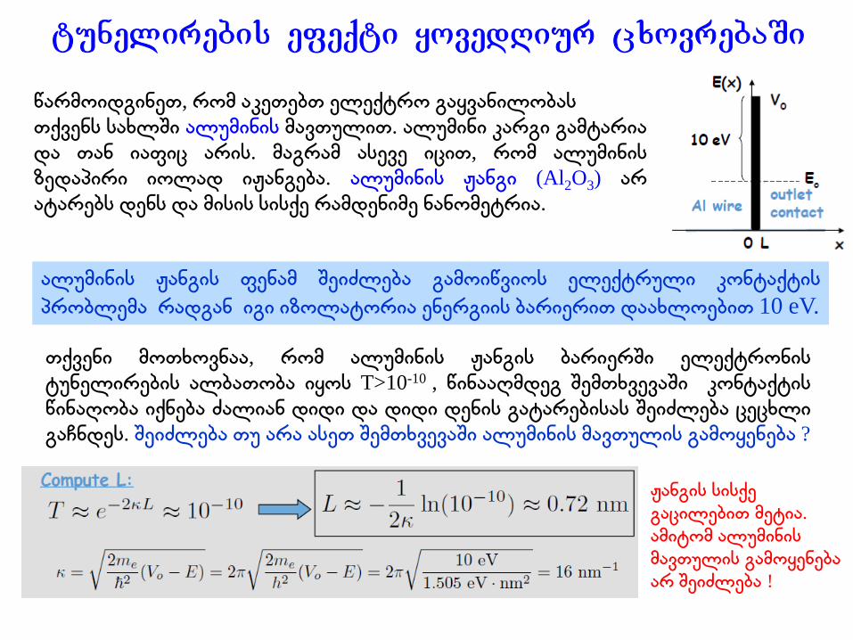
tunelirebis efeqti yovedRiur cxovrebaSi
წარმოიდგინეთ, რომ აკეთებთ ელექტრო გაყვანილობას
თქვენს სახლში ალუმინის მავთულით. ალუმინი კარგი გამტარია
და თან იაფიც არის. მაგრამ ასევე იცით, რომ ალუმინის
ზედაპირი იოლად იჟანგება. ალუმინის ჟანგი (Al2O3) არ
ატარებს დენს და მისის სისქე რამდენიმე ნანომეტრია.
ალუმინის ჟანგის ფენამ შეიძლება გამოიწვიოს ელექტრული კონტაქტის
პრობლემა რადგან იგი იზოლატორია ენერგიის ბარიერით დაახლოებით 10 eV.
თქვენი მოთხოვნაა, რომ ალუმინის ჟანგის ბარიერში ელექტრონის
ტუნელირების ალბათობა იყოს T>10-10 , წინააღმდეგ შემთხვევაში კონტაქტის
წინაღობა იქნება ძალიან დიდი და დიდი დენის გატარებისას შეიძლება ცეცხლი
გაჩნდეს. შეიძლება თუ არა ასეთ შემთხვევაში ალუმინის მავთულის გამოყენება ?
ჟანგის სისქე
გაცილებით მეტია.
ამიტომ ალუმინის
მავთულის გამოყენება
არ შეიძლება !

tunelirebis efeqti
როცა ka >>1, სუსტი ტუნელირება
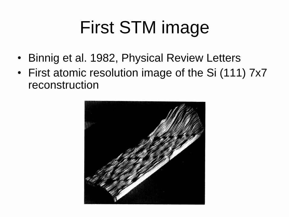
First STM image
• Binnig et al. 1982, Physical Review Letters
• First atomic resolution image of the Si (111) 7x7 reconstruction
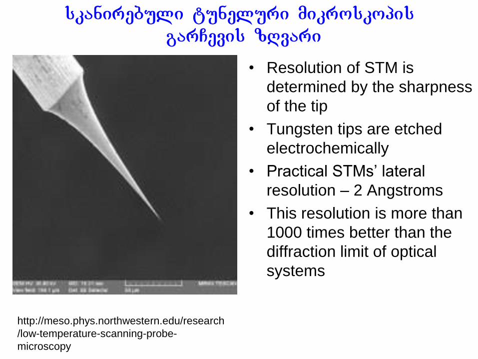
http://meso.phys.northwestern.edu/research
/low-temperature-scanning-probe-
microscopy
• Resolution of STM is
determined by the sharpness
of the tip
• Tungsten tips are etched
electrochemically
• Practical STMs’ lateral
resolution – 2 Angstroms
• This resolution is more than
1000 times better than the
diffraction limit of optical
systems
skanirebuli tuneluri mikroskopis garCevis zRvari
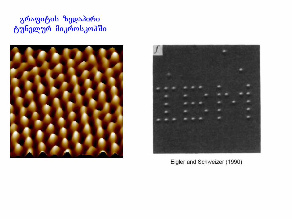
grafitis zedapiri tunelur mikroskopSi
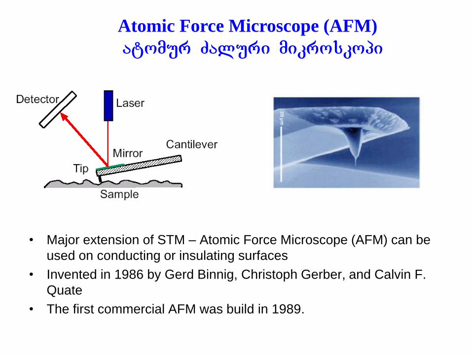
Atomic Force Microscope (AFM) Aatomur Zaluri mikroskopi
• Major extension of STM – Atomic Force Microscope (AFM) can be
used on conducting or insulating surfaces
• Invented in 1986 by Gerd Binnig, Christoph Gerber, and Calvin F.
Quate
• The first commercial AFM was build in 1989.
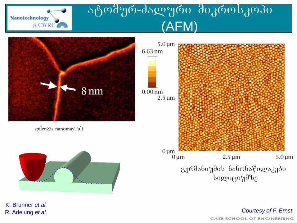
atomur-Zaluri mikroskopi
(AFM)
spilenZis nanomavTuli
R. Adelung et al.
germaniumis nanonawilakebi siliciumze
K. Brunner et al. Courtesy of F. Ernst
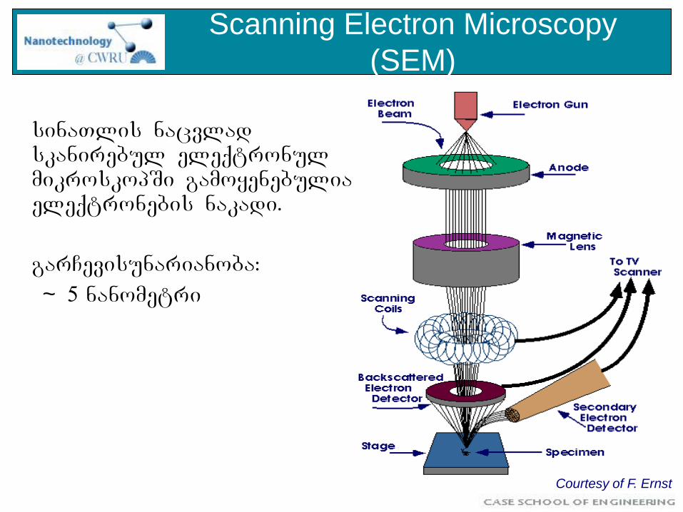
Scanning Electron Microscopy
(SEM)
sinaTlis nacvlad skanirebul eleqtronul mikroskopSi gamoyenebulia eleqtronebis nakadi.
garCevisunarianoba:
~ 5 nanometri
Courtesy of F. Ernst
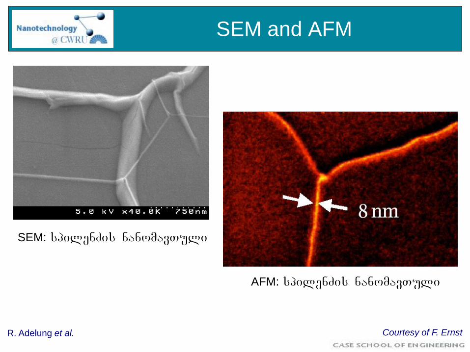
SEM and AFM
SEM: spilenZis nanomavTuli
R. Adelung et al. Courtesy of F. Ernst
AFM: spilenZis nanomavTuli
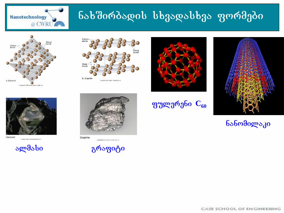
naxSirbadis sxvadasxva formebi
almasi grafiti
fulereni C60
nanomilaki
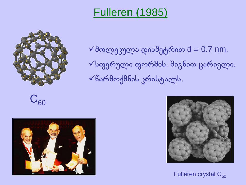
Fulleren (1985)
მოლეკულა დიამეტრით d = 0.7 nm.
სფერული ფორმის, შიგნით ცარიელი.
წარმოქმნის კრისტალს.
С60
Fulleren crystal С60
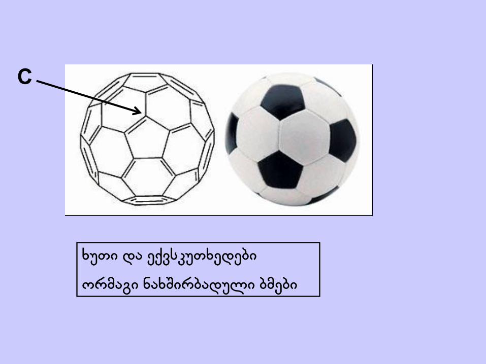
ხუთი და ექვსკუთხედები
ორმაგი ნახშირბადული ბმები
С
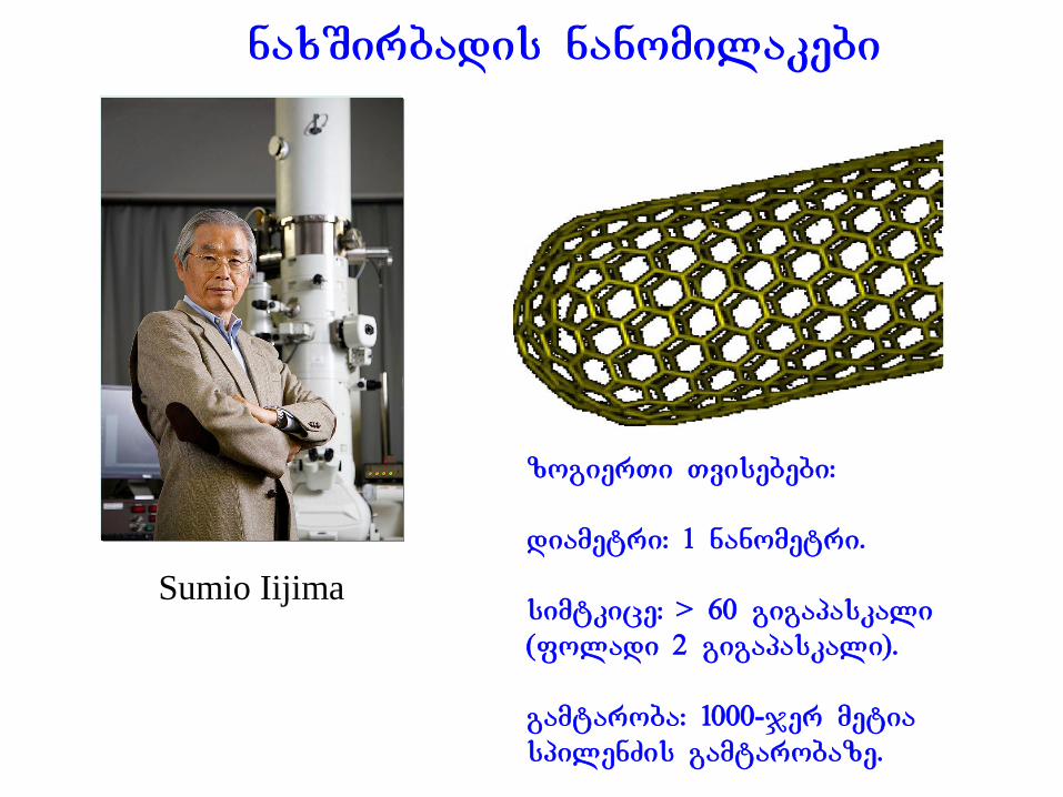
naxSirbadis nanomilakebi
zogierTi Tvisebebi: diametri: 1 nanometri. simtkice: > 60 gigapaskali (foladi 2 gigapaskali). gamtaroba: 1000-jer metia spilenZis gamtarobaze.
Sumio Iijima
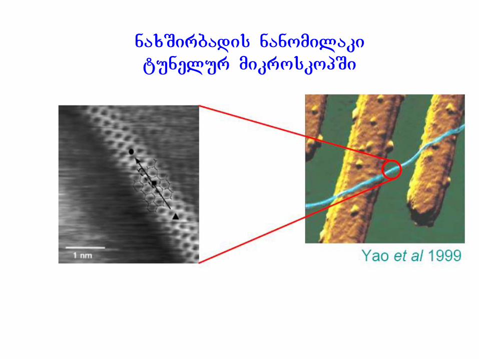
naxSirbadis nanomilaki tunelur mikroskopSi
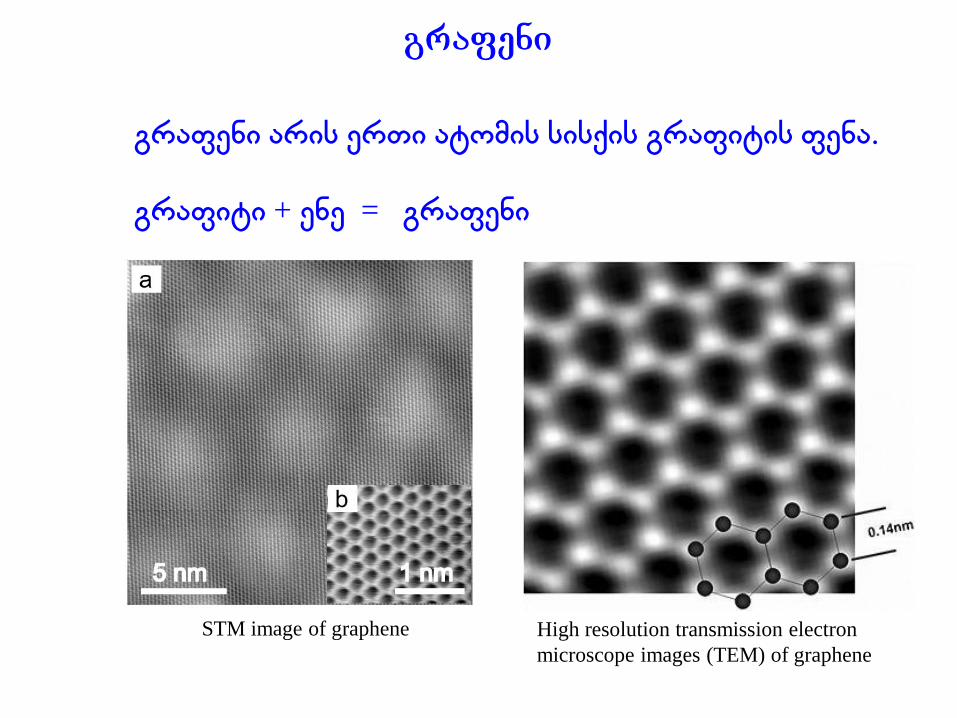
Ggrafeni
High resolution transmission electron
microscope images (TEM) of graphene
გრაფენი არის ერთი ატომის სისქის გრაფიტის ფენა.
გრაფიტი + ენე = გრაფენი
STM image of graphene
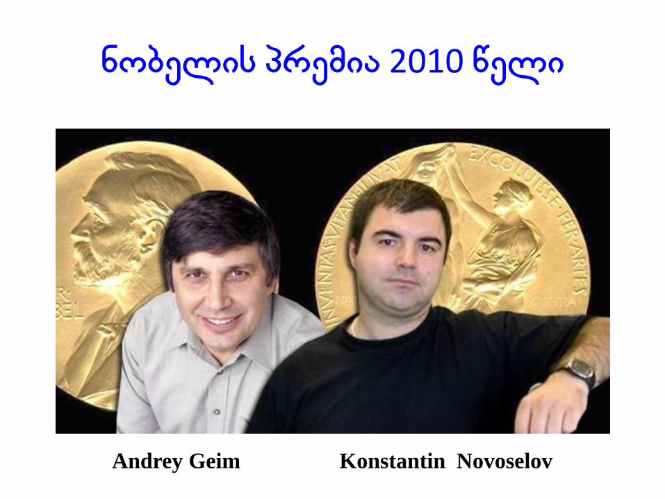
ნობელის პრემია 2010 წელი
Andrey Geim Konstantin Novoselov
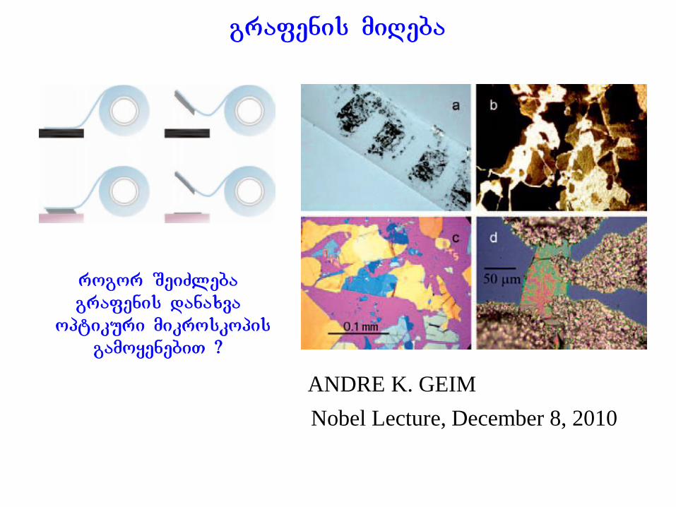
Ggrafenis miReba
ANDRE K. GEIM
Nobel Lecture, December 8, 2010
rogor SeiZleba grafenis danaxva
Ooptikuri mikroskopis gamoyenebiT ?
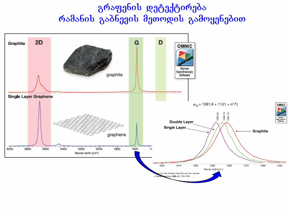
grafenis deteqtireba ramanis gabnevis meTodis gamoyenebiT
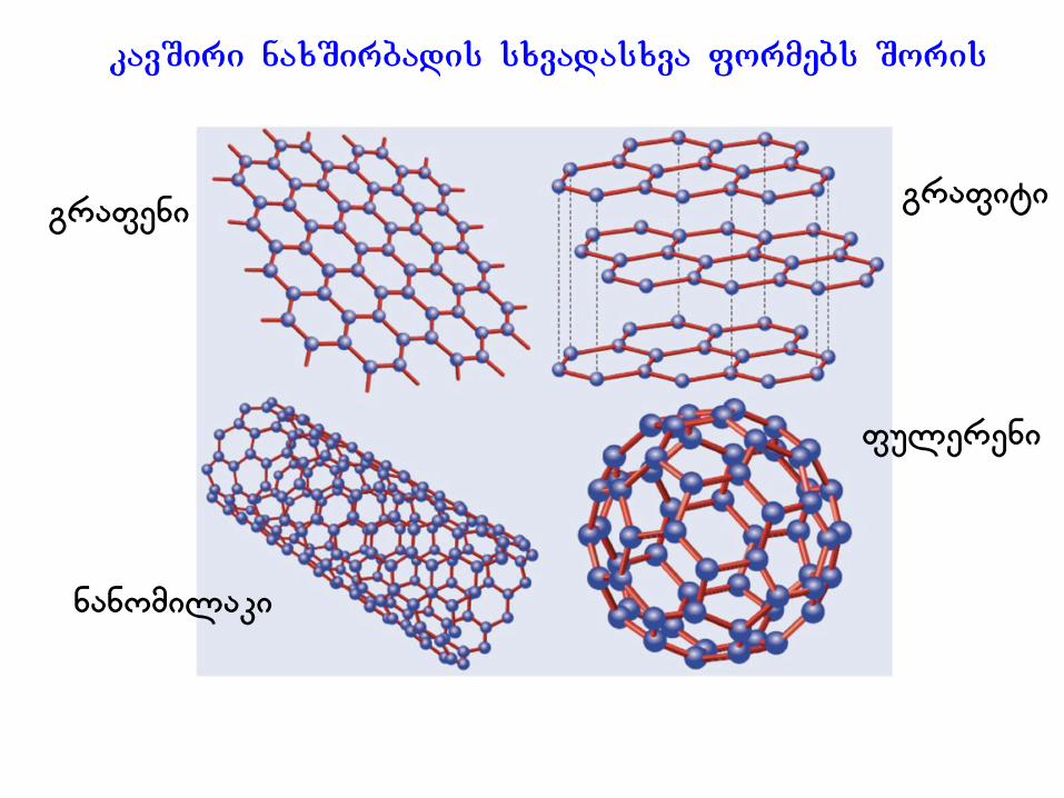
kavSiri naxSirbadis sxvadasxva formebs Soris
გრაფენი გრაფიტი
ნანომილაკი
ფულერენი
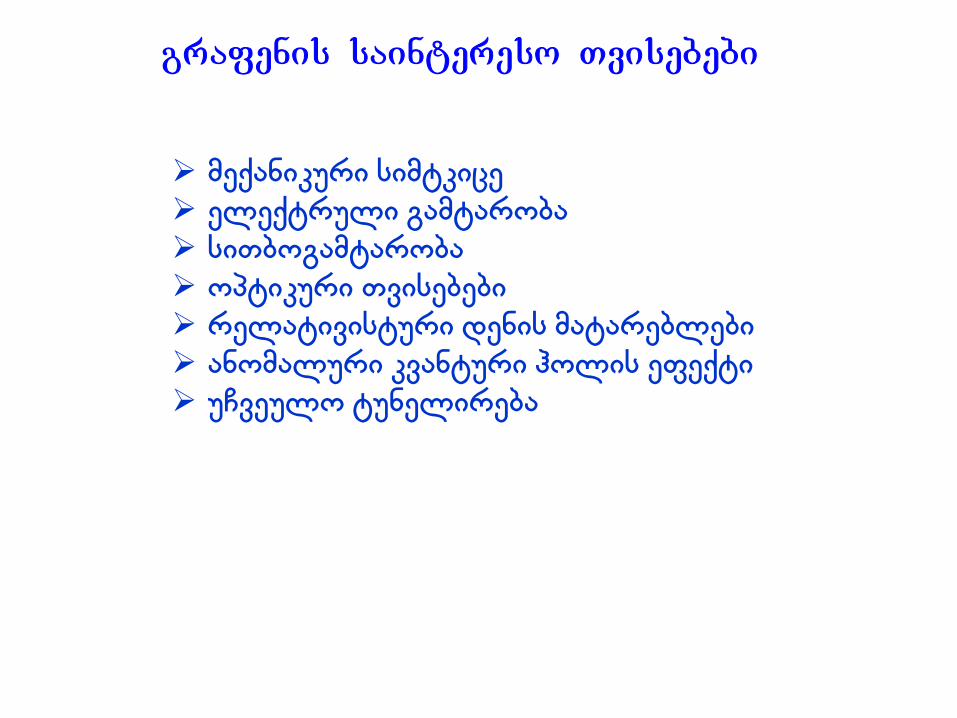
Ggrafenis saintereso Tvisebebi
მექანიკური სიმტკიცე
ელექტრული გამტარობა
სითბოგამტარობა
ოპტიკური თვისებები
რელატივისტური დენის მატარებლები
ანომალური კვანტური ჰოლის ეფექტი
უჩვეულო ტუნელირება
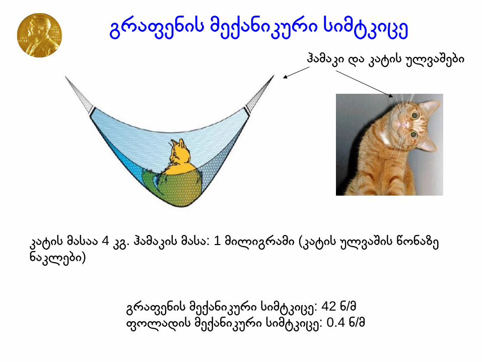
გრაფენის მექანიკური სიმტკიცე
კატის მასაა 4 კგ. ჰამაკის მასა: 1 მილიგრამი (კატის ულვაშის წონაზე ნაკლები)
ჰამაკი და კატის ულვაშები
გრაფენის მექანიკური სიმტკიცე: 42 ნ/მ ფოლადის მექანიკური სიმტკიცე: 0.4 ნ/მ
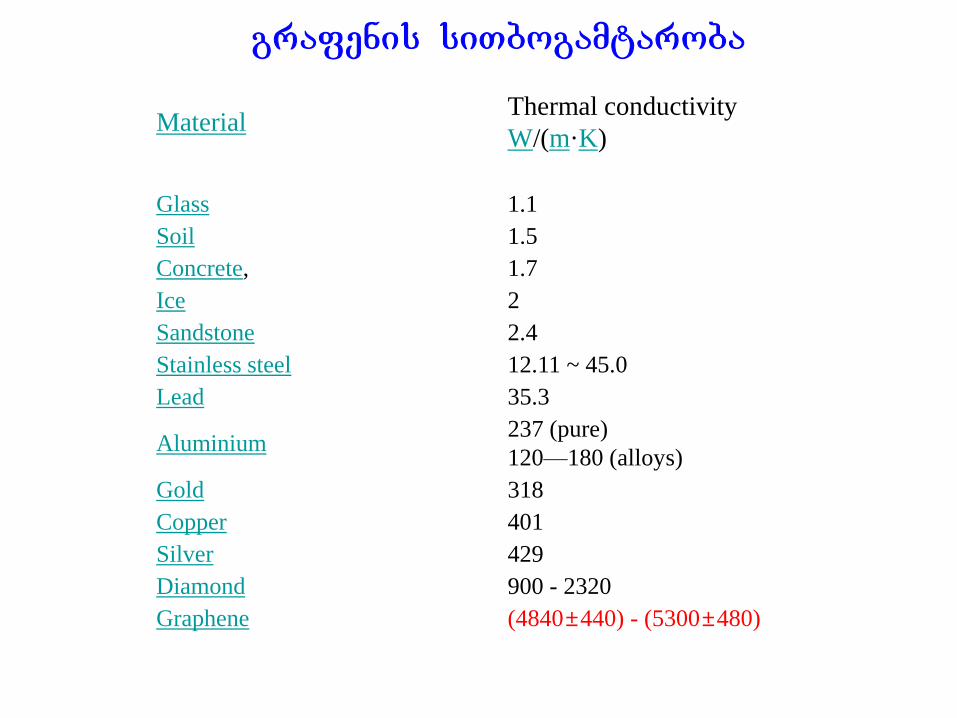
grafenis siTbogamtaroba
Material Thermal conductivity
W/(m·K)
Glass 1.1
Soil 1.5
Concrete, 1.7
Ice 2
Sandstone 2.4
Stainless steel 12.11 ~ 45.0
Lead 35.3
Aluminium 237 (pure)
120—180 (alloys)
Gold 318
Copper 401
Silver 429
Diamond 900 - 2320
Graphene (4840±440) - (5300±480)
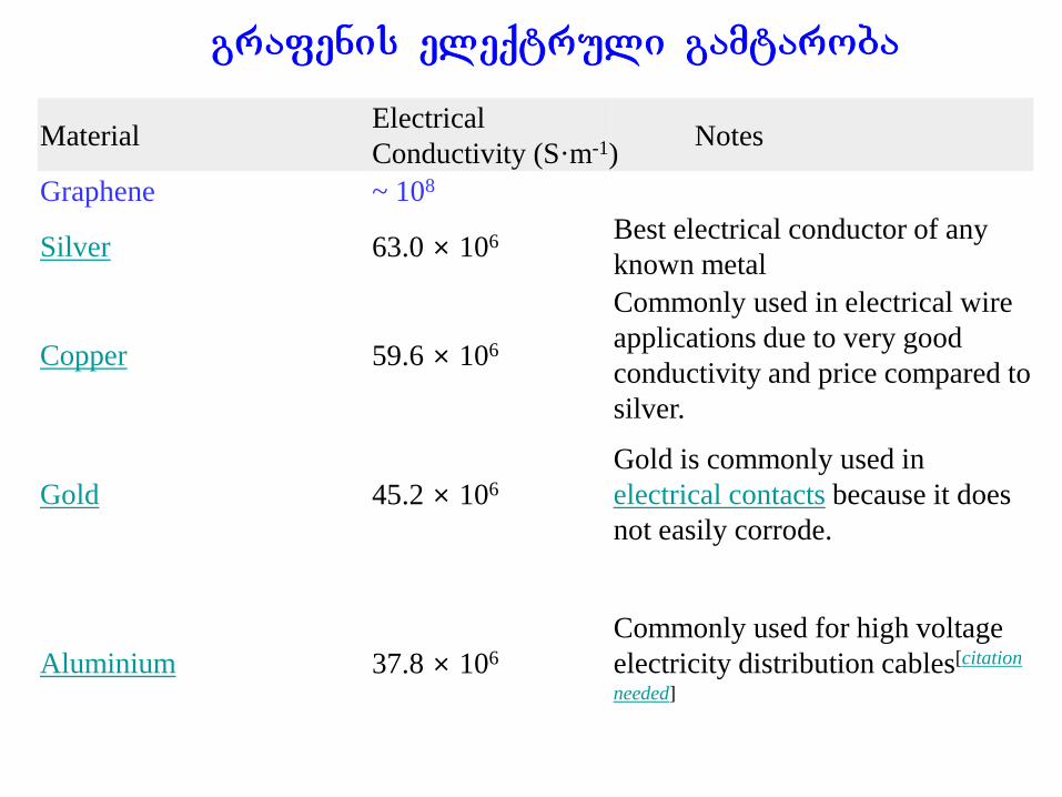
Ggrafenis eleqtruli gamtaroba
Material Electrical
Conductivity (S·m-1) Notes
Graphene ~ 108
Silver 63.0 × 10⁶ Best electrical conductor of any
known metal
Copper 59.6 × 10⁶
Commonly used in electrical wire
applications due to very good
conductivity and price compared to
silver.
Gold 45.2 × 10⁶
Gold is commonly used in
electrical contacts because it does
not easily corrode.
Aluminium 37.8 × 10⁶
Commonly used for high voltage
electricity distribution cables[citation
needed]
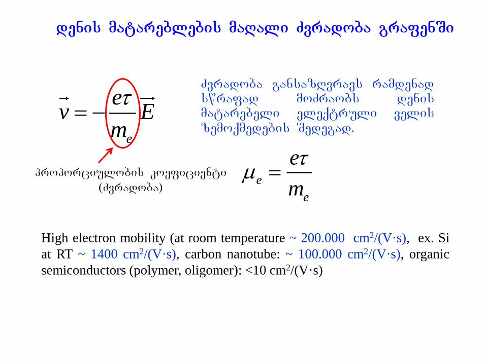
Ddenis matareblebis maRali Zvradoba grafenSi
High electron mobility (at room temperature ~ 200.000 cm2/(V·s), ex. Si
at RT ~ 1400 cm2/(V·s), carbon nanotube: ~ 100.000 cm2/(V·s), organic
semiconductors (polymer, oligomer): <10 cm2/(V·s)
e
ev E
m
e
e
e
m
proporciulobis koeficienti
(Zvradoba)
Zvradoba gansazRvravs ramdenad swrafad moZraobs denis matarebeli eleqtruli velis zemoqmedebis Sedegad.
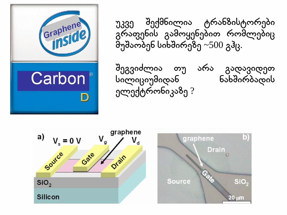
უკვე შექმნილია ტრანზისტორები
გრაფენის გამოყენებით რომლებიც
მუშაობენ სიხშირეზე ~500 გჰც.
შეგვიძლია თუ არა გადავიდეთ
სილიციუმიდან ნახშირბადის
ელექტრონიკაზე ?
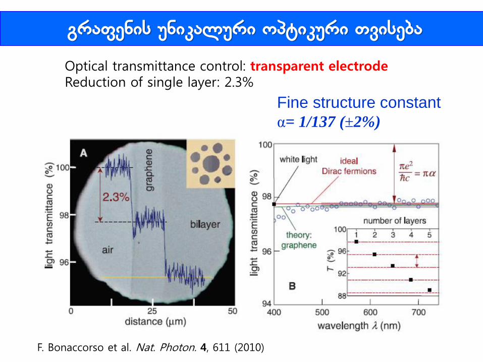
გრაფენის უნიკალური ოპტიკური თვისება
Optical transmittance control: transparent electrode Reduction of single layer: 2.3%
F. Bonaccorso et al. Nat. Photon. 4, 611 (2010)
Fine structure constant
α= 1/137 (±2%)
grafenis realurad arsebobasTan dakavSirebuli kiTxvebi: • ratom aris saerTod SesaZlebeli atomuri
sisqis uwyveti fenis miReba ?
• ratom aris organzomilebiani atomuri sisqis fena Termodinamikurad stabiluri ?
• ratom aris grafeni qimiurad inertuli da stabiluri haeris atmosferoSi oTaxis temperaturaze ?
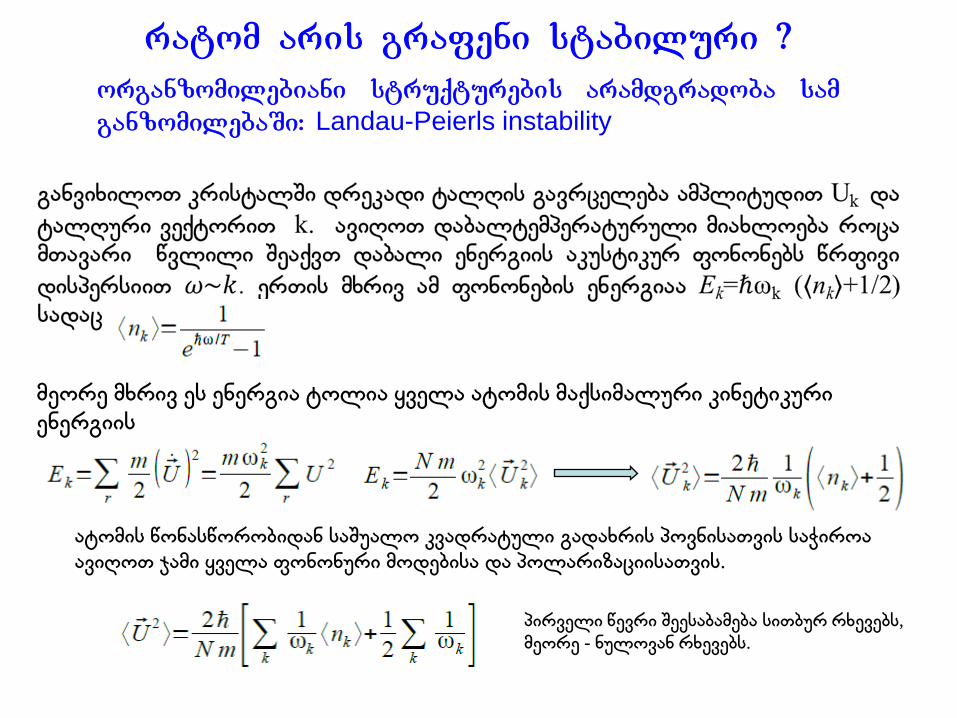
ratom aris grafeni stabiluri ?
organzomilebiani struqturebis aramdgradoba sam ganzomilebaSi: Landau-Peierls instability
მეორე მხრივ ეს ენერგია ტოლია ყველა ატომის მაქსიმალური კინეტიკური
ენერგიის
ატომის წონასწორობიდან საშუალო კვადრატული გადახრის პოვნისათვის საჭიროა
ავიღოთ ჯამი ყველა ფონონური მოდებისა და პოლარიზაციისათვის.
პირველი წევრი შეესაბამება სითბურ რხევებს,
მეორე - ნულოვან რხევებს.
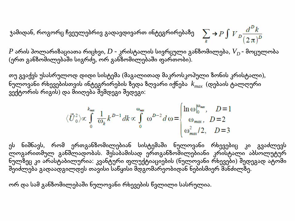
ჯამიდან, როგორც ჩვეულებრივ გადავდივართ ინტეგრირებაზე
P არის პოლარიზაციათა რიცხვი, D - კრისტალის სივრცული განზომილება, VD - მოცულობა
(ერთ განზომილებაში სიგრძე, ორ განზომილებაში ფართობი).
თუ გვაქვს უსასრულოდ დიდი სისტემა (მაგალითად მაკროსკოპული ზონის კრისტალი),
ნულოვანი რხევებისთვის ინტეგრირების ზედა ზღვარი იქნება kmax (დებაის ტალღური
ვექტორის რიგის) და მიიღება შემდეგი შედეგი:
ეს ნიშნავს, რომ ერთგანზომილებიან სისტემაში ნულოვანი რხევებიც კი გვაძლევს
ლოგარითმულ განშლადობას. შესაბამისად ერთგანზომილებიანი კრისტალი აბსოლუტურ
ნულზეც კი არასტაბილურია: კვანტური ფლუქტიაციების (ნულოვანი რხევები) შედეგად ატომი
შეიძლება გადაადგილდეს თავისი საწყისი მდგომარეობიდან ნებისმიერ მანძილზე.
ორ და სამ განზომილებაში ნულოვანი რხევების წვლილი სასრულია.
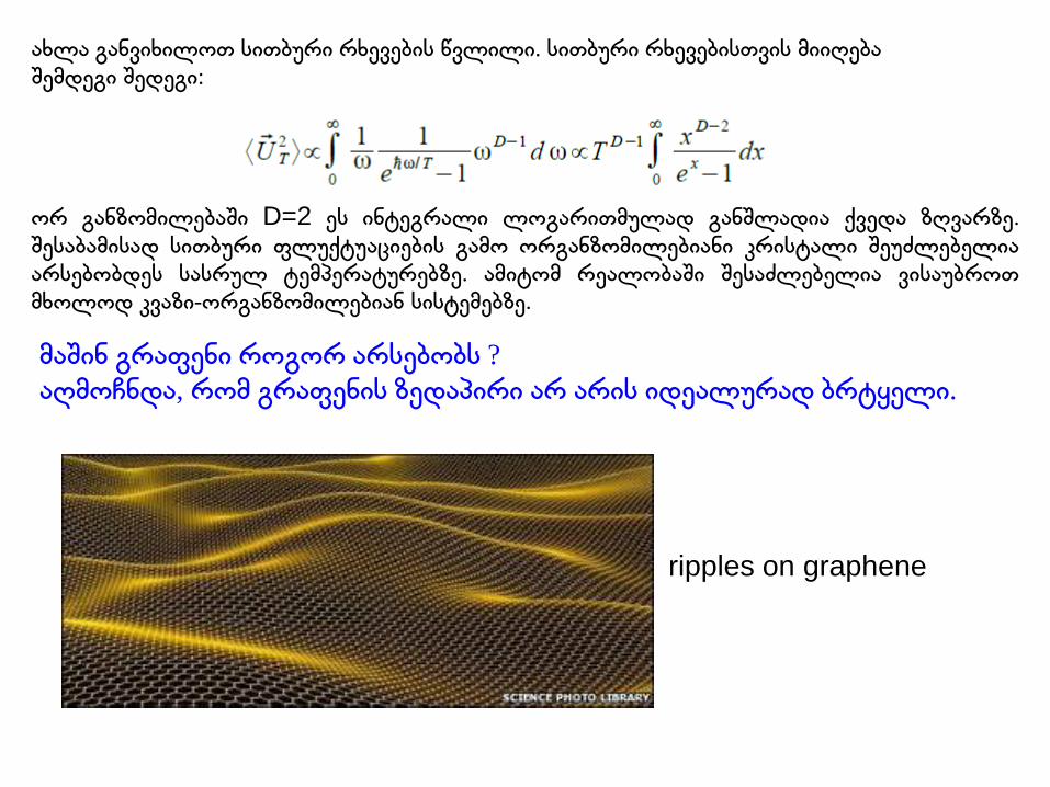
ახლა განვიხილოთ სითბური რხევების წვლილი. სითბური რხევებისთვის მიიღება
შემდეგი შედეგი:
ორ განზომილებაში D=2 ეს ინტეგრალი ლოგარითმულად განშლადია ქვედა ზღვარზე.
შესაბამისად სითბური ფლუქტუაციების გამო ორგანზომილებიანი კრისტალი შეუძლებელია
არსებობდეს სასრულ ტემპერატურებზე. ამიტომ რეალობაში შესაძლებელია ვისაუბროთ
მხოლოდ კვაზი-ორგანზომილებიან სისტემებზე.
მაშინ გრაფენი როგორ არსებობს ?
აღმოჩნდა, რომ გრაფენის ზედაპირი არ არის იდეალურად ბრტყელი.
ripples on graphene
ლექცია II
Gგრაფენის ელექტრონული სტრუქტურა
prof. aleqsandre Sengelaia
ivane javaxiSvilis sax. Tbilisis
saxelmwifo universiteti
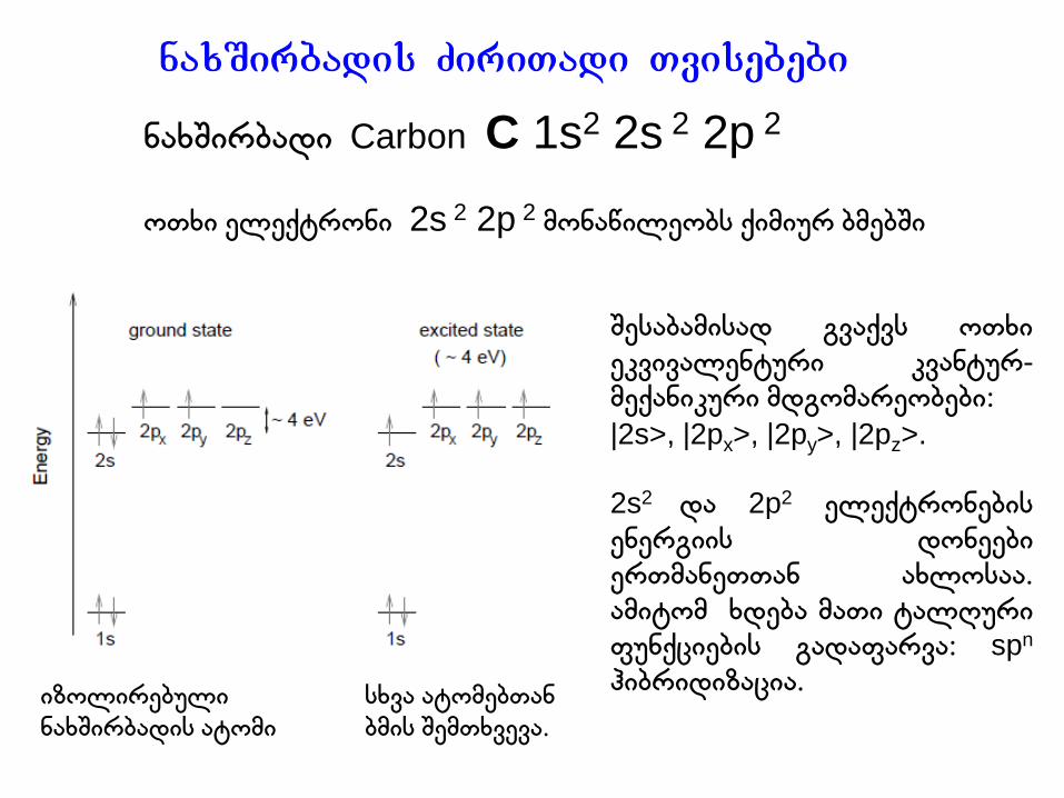
naxSirbadis ZiriTadi Tvisebebi
ნახშირბადი Carbon C 1s2 2s 2 2p 2
ოთხი ელექტრონი 2s 2 2p 2 მონაწილეობს ქიმიურ ბმებში
შესაბამისად გვაქვს ოთხი
ეკვივალენტური კვანტურ-
მექანიკური მდგომარეობები:
|2s>, |2px>, |2py>, |2pz>.
2s2 და 2p2 ელექტრონების
ენერგიის დონეები
ერთმანეთთან ახლოსაა.
ამიტომ ხდება მათი ტალღური
ფუნქციების გადაფარვა: spn
ჰიბრიდიზაცია.
იზოლირებული
ნახშირბადის ატომი
სხვა ატომებთან
ბმის შემთხვევა.
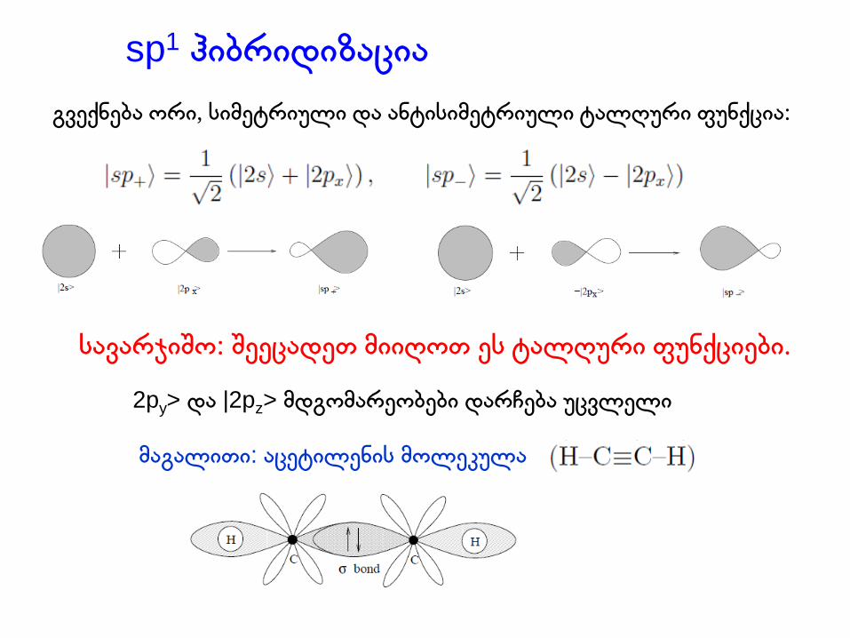
sp1 ჰიბრიდიზაცია
გვექნება ორი, სიმეტრიული და ანტისიმეტრიული ტალღური ფუნქცია:
2py> და |2pz> მდგომარეობები დარჩება უცვლელი
მაგალითი: აცეტილენის მოლეკულა
სავარჯიშო: შეეცადეთ მიიღოთ ეს ტალღური ფუნქციები.
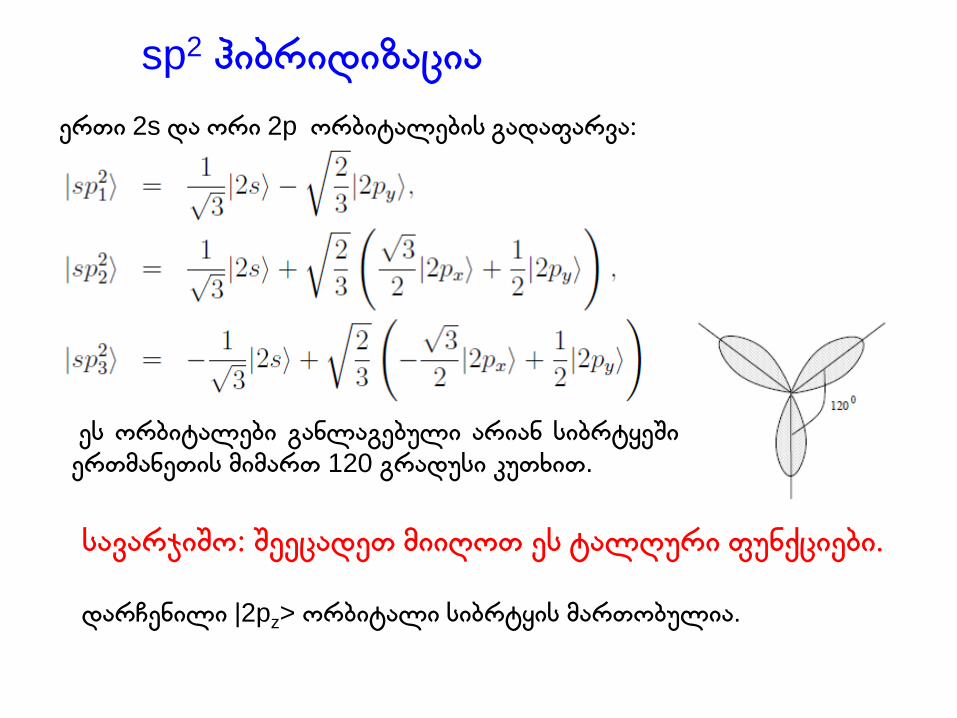
sp2 ჰიბრიდიზაცია
ერთი 2s და ორი 2p ორბიტალების გადაფარვა:
დარჩენილი |2pz> ორბიტალი სიბრტყის მართობულია.
ეს ორბიტალები განლაგებული არიან სიბრტყეში ერთმანეთის მიმართ 120 გრადუსი კუთხით.
სავარჯიშო: შეეცადეთ მიიღოთ ეს ტალღური ფუნქციები.
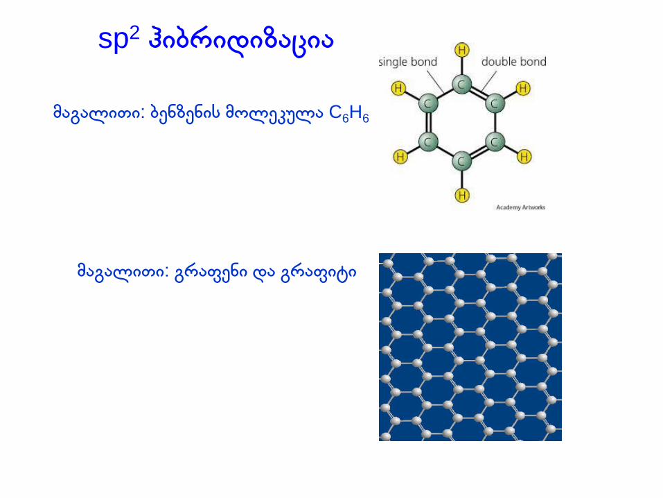
sp2 ჰიბრიდიზაცია
მაგალითი: გრაფენი და გრაფიტი
მაგალითი: ბენზენის მოლეკულა C6H6
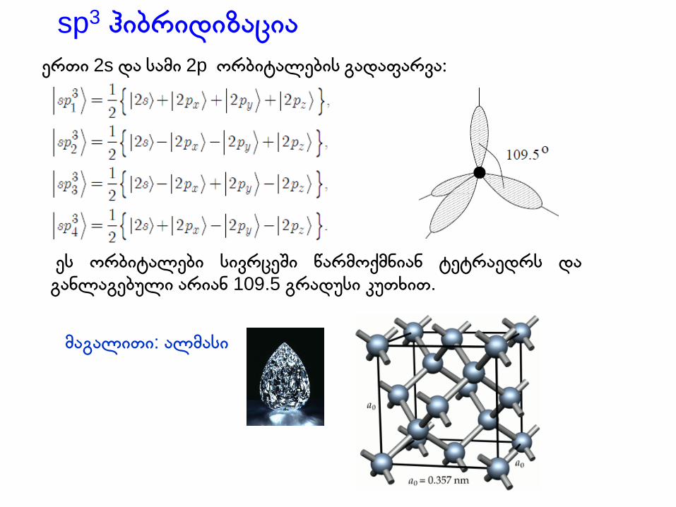
sp3 ჰიბრიდიზაცია ერთი 2s და სამი 2p ორბიტალების გადაფარვა:
ეს ორბიტალები სივრცეში წარმოქმნიან ტეტრაედრს და განლაგებული არიან 109.5 გრადუსი კუთხით.
მაგალითი: ალმასი
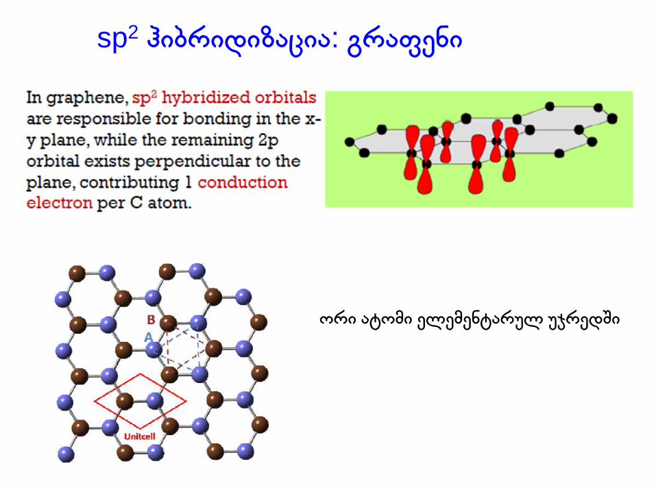
sp2 ჰიბრიდიზაცია: გრაფენი
ორი ატომი ელემენტარულ უჯრედში
Crystal Structure 8
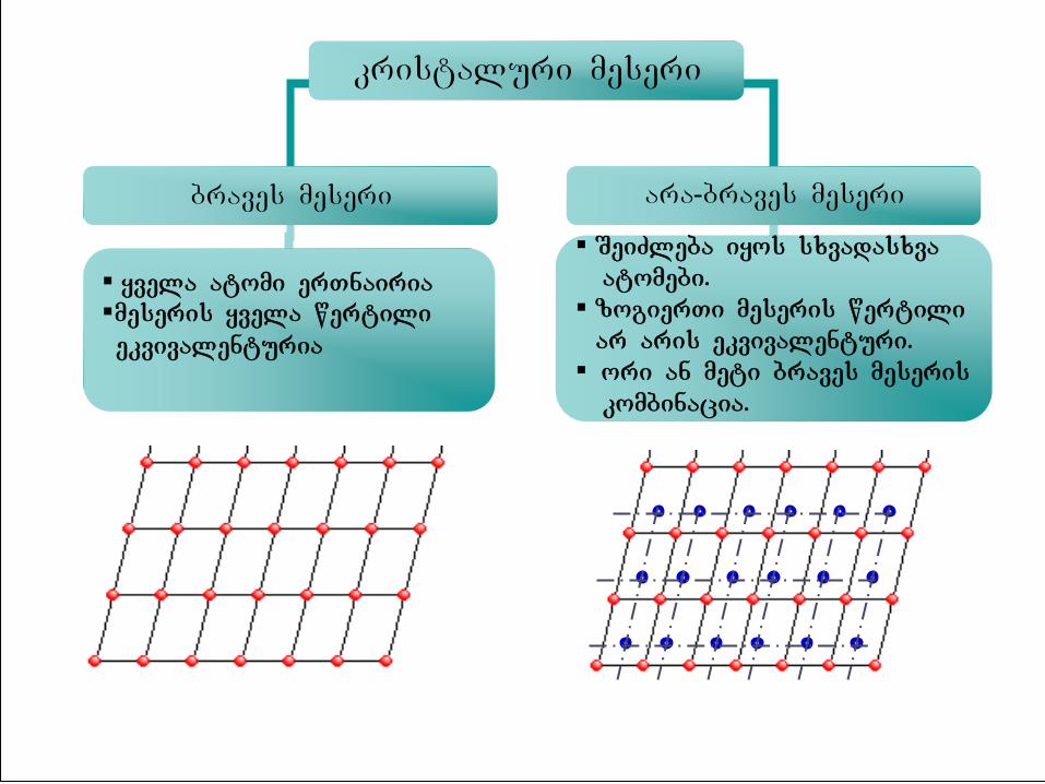
kristaluri meseri
braves meseri ara-braves meseri
yvela atomi erTnairia
meseris yvela wertili ekvivalenturia
SeiZleba iyos sxvadasxva atomebi. zogierTi meseris wertili ar aris ekvivalenturi. ori an meti braves meseris kombinacia.
Crystal Structure 9
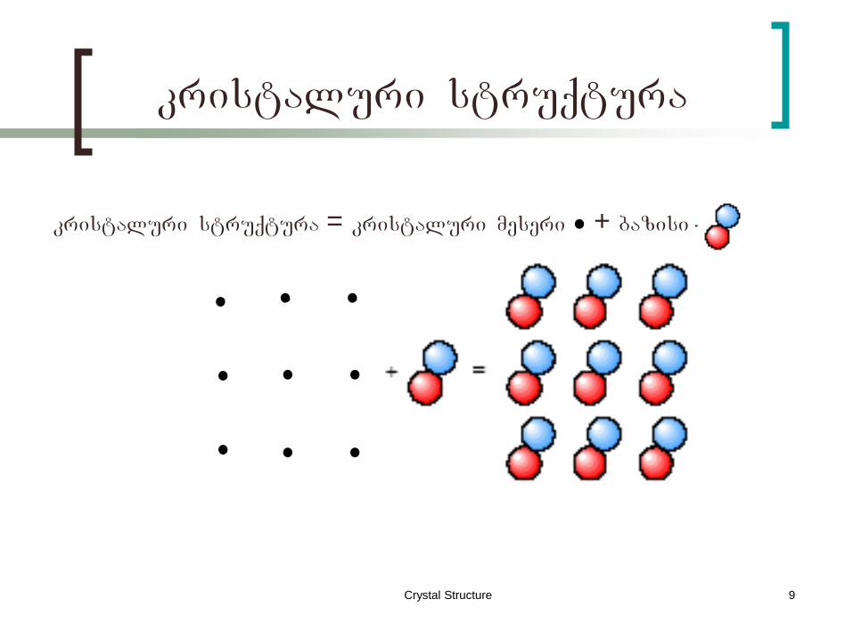
kristaluri struqtura
kristaluri struqtura = kristaluri meseri + bazisi
Crystal Structure 10
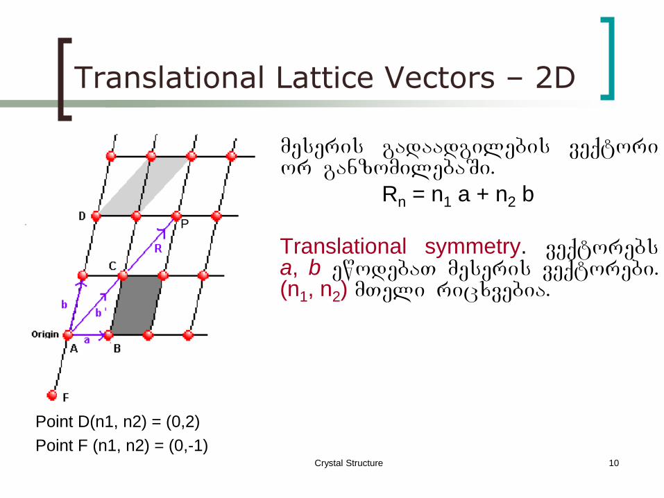
Translational Lattice Vectors – 2D
meseris gadaadgilebis veqtori or ganzomilebaSi.
Rn = n1 a + n2 b
Translational symmetry. veqtorebs
a, b ewodebaT meseris veqtorebi. (n1, n2) mTeli ricxvebia.
P
Point D(n1, n2) = (0,2)
Point F (n1, n2) = (0,-1)
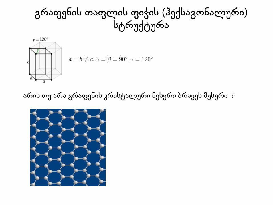
გრაფენის თაფლის ფიჭის (ჰექსაგონალური) სტრუქტურა
არის თუ არა გრაფენის კრისტალური მესერი ბრავეს მესერი ?
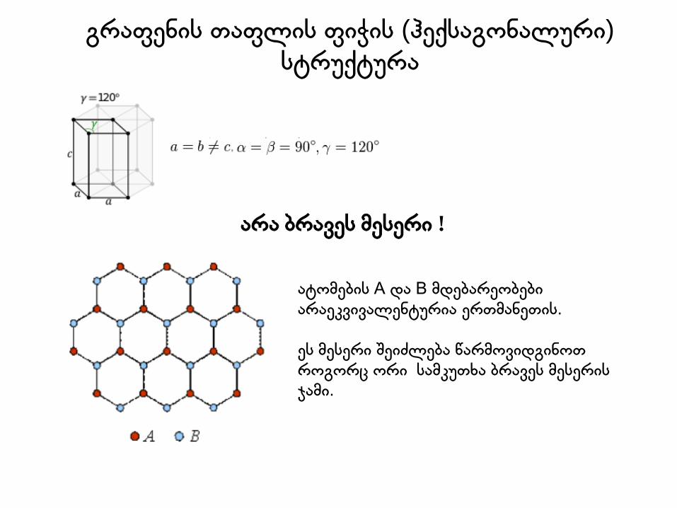
გრაფენის თაფლის ფიჭის (ჰექსაგონალური) სტრუქტურა
ატომების А და В მდებარეობები არაეკვივალენტურია ერთმანეთის. ეს მესერი შეიძლება წარმოვიდგინოთ
როგორც ორი სამკუთხა ბრავეს მესერის ჯამი.
არა ბრავეს მესერი !
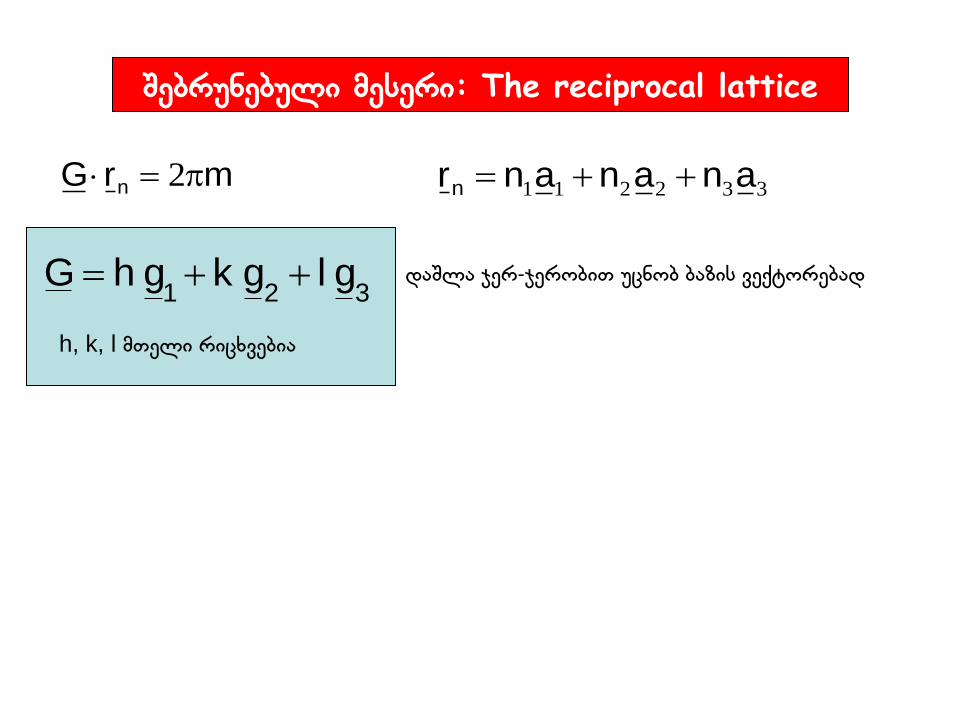
mrG n 2332211 anananrn
დაშლა ჯერ-ჯერობით უცნობ ბაზის ვექტორებად 321
glgkghG
h, k, l მთელი რიცხვებია
შებრუნებული მესერი: The reciprocal lattice
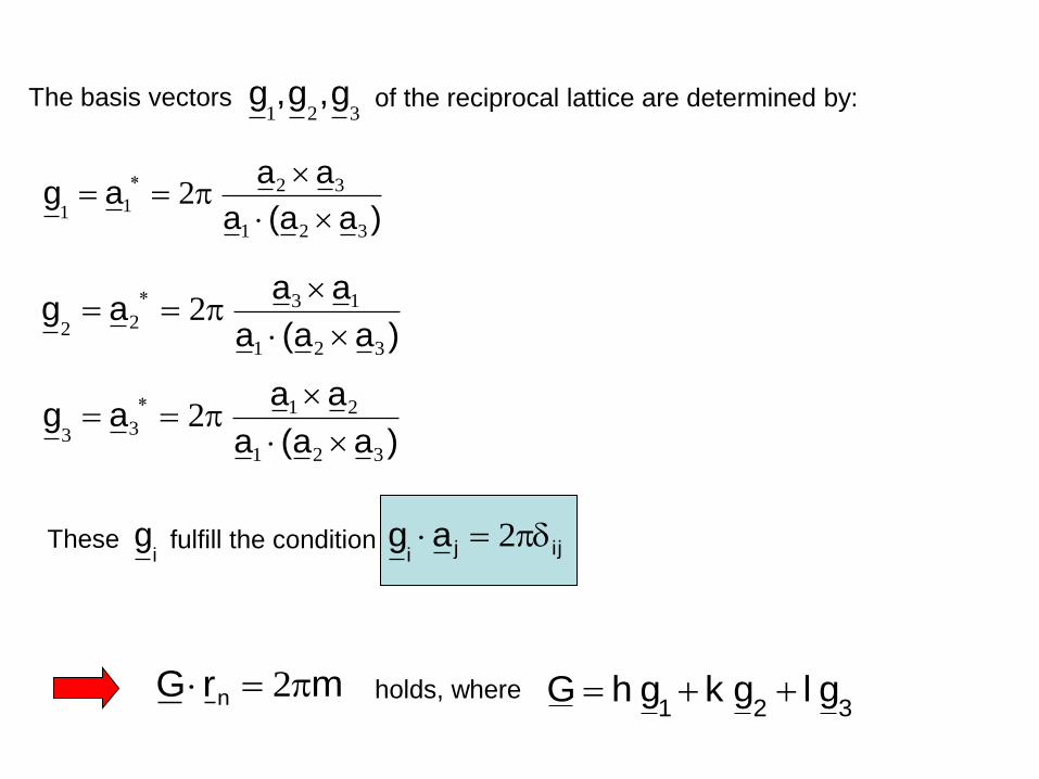
321g,g,gThe basis vectors of the reciprocal lattice are determined by:
)aa(a
aaag
321
3211
2
)aa(a
aaag
321
1322
2
)aa(a
aaag
321
2133
2
igThese fulfill the condition ijji
ag 2
mrG n 2 holds, where 321
glgkghG
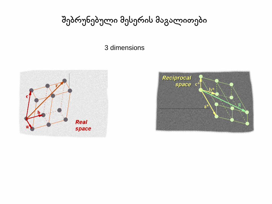
შებრუნებული მესერის მაგალითები
3 dimensions
16
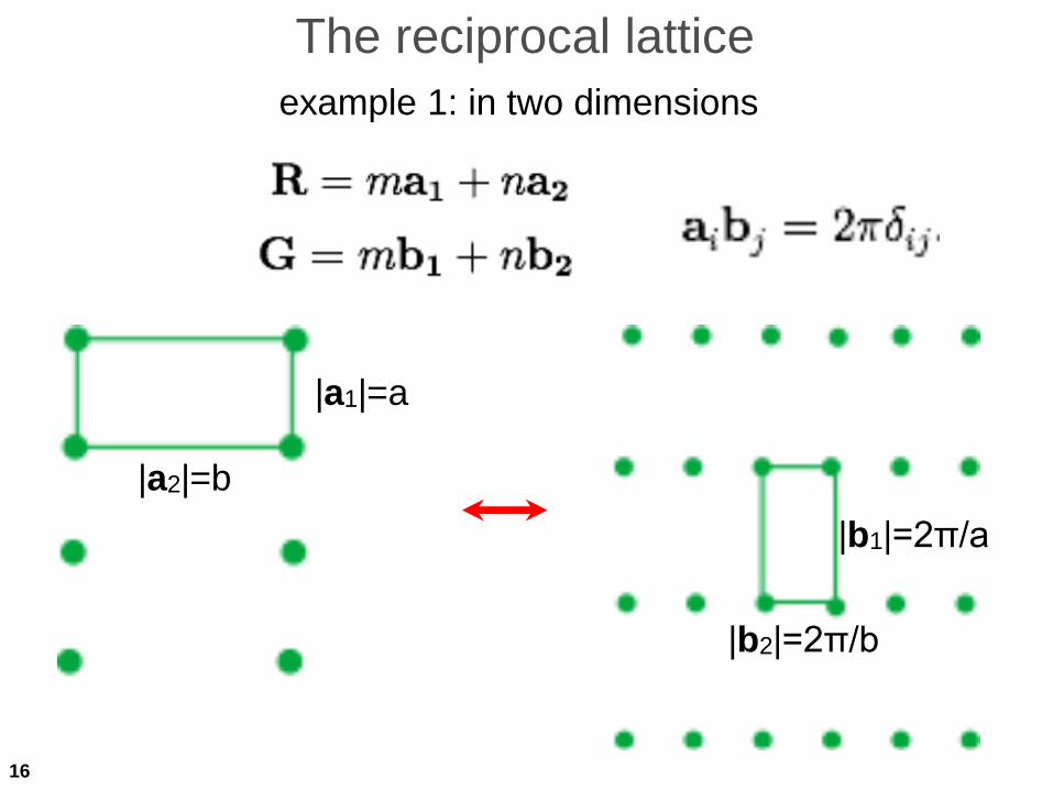
The reciprocal lattice
example 1: in two dimensions
|a1|=a
|a2|=b
|b2|=2π/b
|b1|=2π/a
17
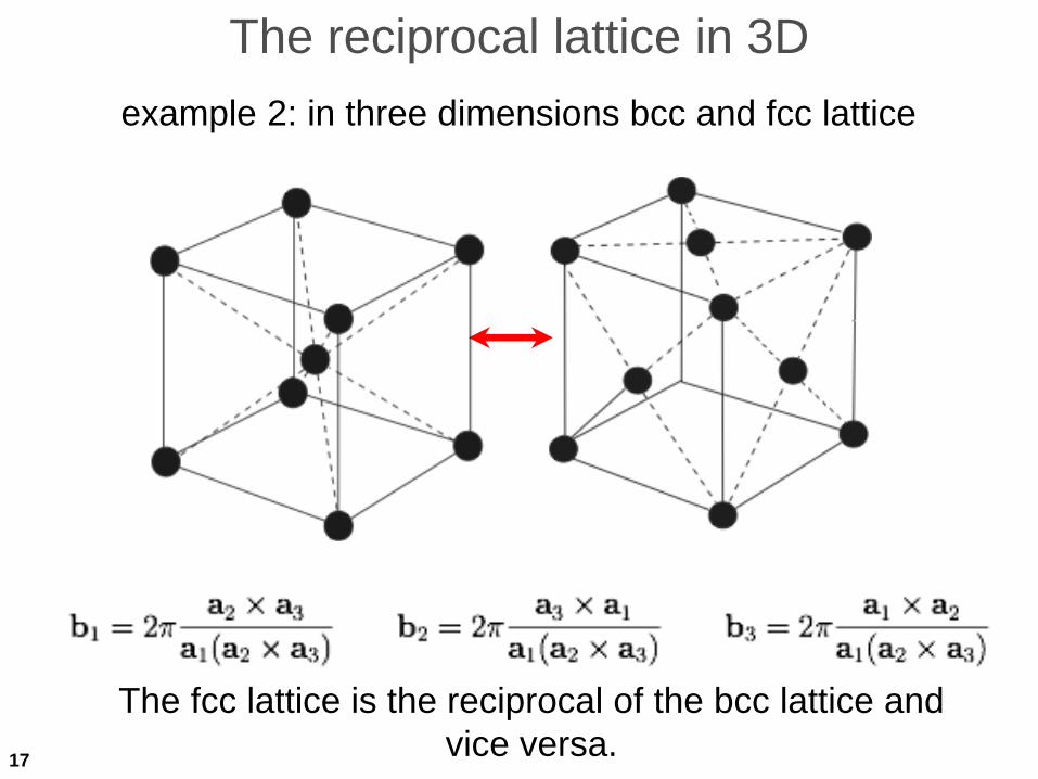
The reciprocal lattice in 3D
example 2: in three dimensions bcc and fcc lattice
The fcc lattice is the reciprocal of the bcc lattice and
vice versa.
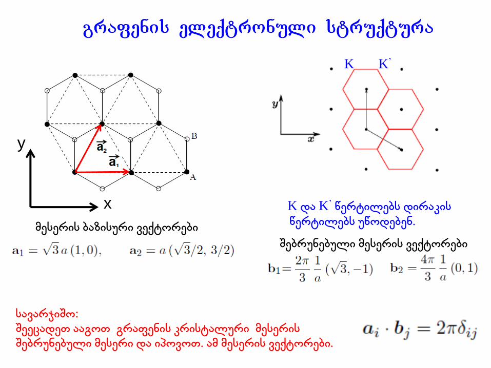
Ggrafenis eleqtronuli struqtura
მესერის ბაზისური ვექტორები
შებრუნებული მესერის ვექტორები
x
y
სავარჯიშო:
შეეცადეთ ააგოთ გრაფენის კრისტალური მესერის
შებრუნებული მესერი და იპოვოთ. ამ მესერის ვექტორები.
K და K’ წერტილებს დირაკის
წერტილებს უწოდებენ.
K K’
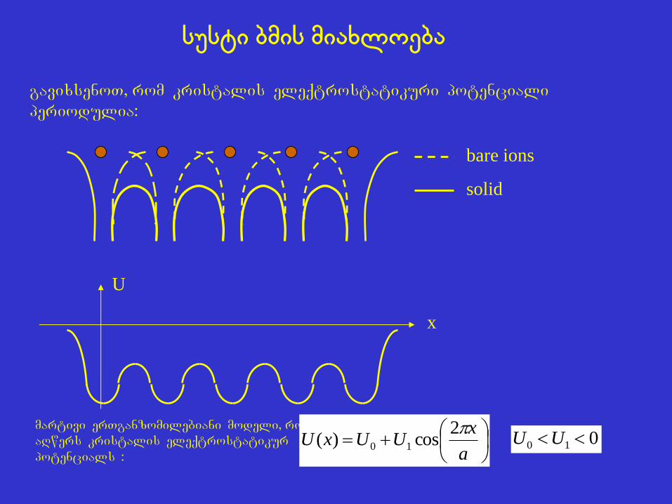
სუსტი ბმის მიახლოება
gavixsenoT, rom kristalis eleqtrostatikuri potenciali periodulia:
bare ions
solid
martivi erTganzomilebiani modeli, romelic aRwers kristalis eleqtrostatikur potencials :
a
xUUxU
2cos)( 10
U
x
010 UU
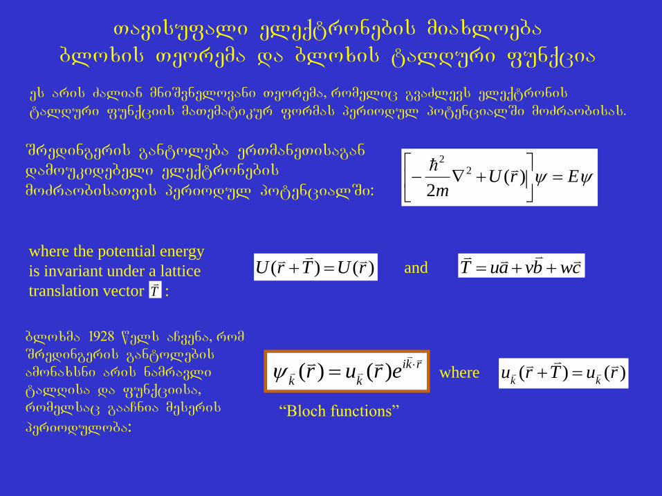
Tavisufali eleqtronebis miaxloeba bloxis Teorema da bloxis talRuri funqcia
es aris Zalian mniSvnelovani Teorema, romelic gvaZlevs eleqtronis talRuri funqciis maTematikur formas periodul potencialSi moZraobisas.
Sredingeris gantoleba erTmaneTisagan damoukidebeli eleqtronebis moZraobisaTvis periodul potencialSi:
ErUm
)(
2
22
)()( rUTrU
where the potential energy
is invariant under a lattice
translation vector : T
bloxma 1928 wels aCvena, rom Sredingeris gantolebis amonaxsni aris namravli talRisa da funqciisa, romelsac gaaCnia meseris
perioduloba:
rki
kkerur
)()(
“Bloch functions”
)()( ruTrukk
where
cwbvauT
and
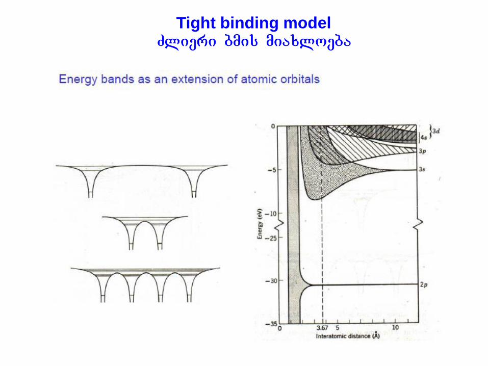
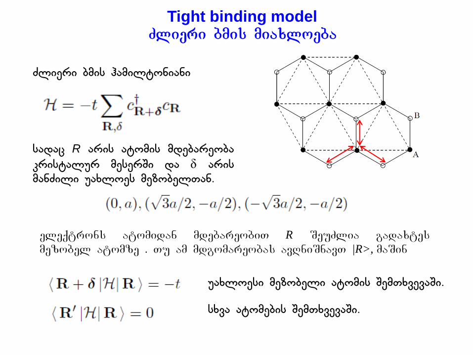
Tight binding model Zlieri bmis miaxloeba
Tight binding model Zlieri bmis miaxloeba
ძლიერი ბმის ჰამილტონიანი
სადაც R არის ატომის მდებარეობა კრისტალურ მესერში და δ არის მანძილი უახლოეს მეზობელთან.
eleqtrons atomidan mdebareobiT R SeuZlia gadaxtes mezobel atomze . Tu am mdgomareobas avRniSnavT |R>, maSin
უახლოესი მეზობელი ატომის შემთხვევაში.
სხვა ატომების შემთხვევაში.
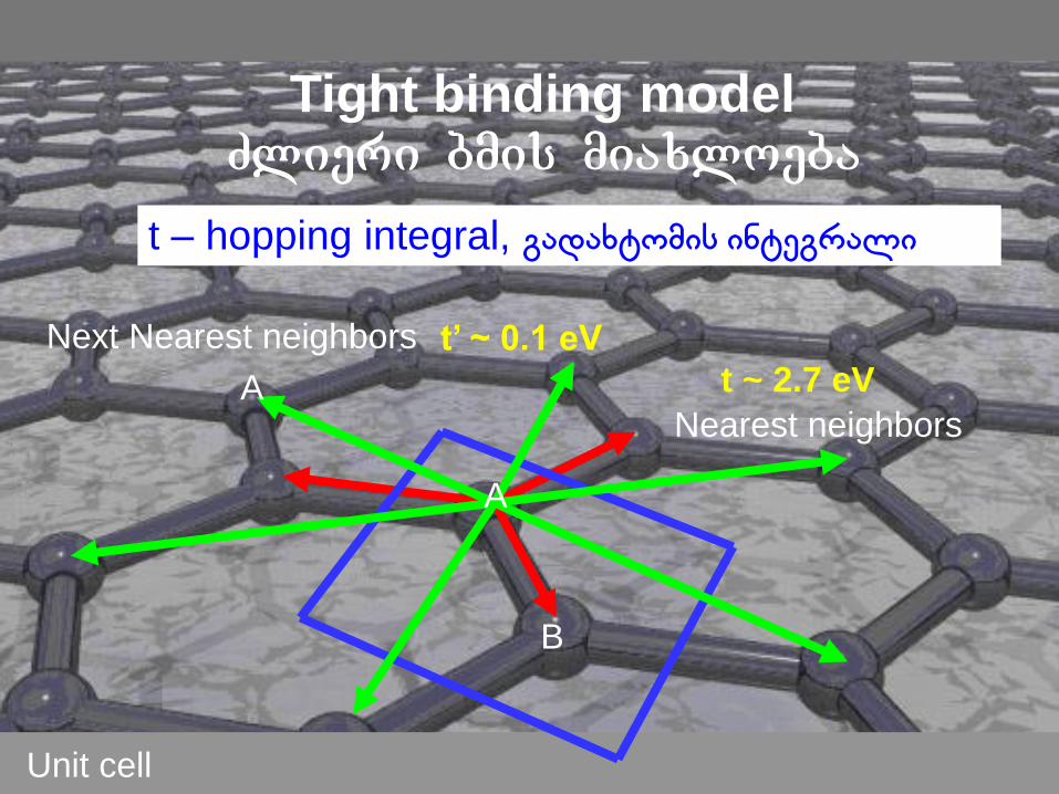
t ~ 2.7 eV
B
t’ ~ 0.1 eV
A
A
Unit cell
Nearest neighbors
Next Nearest neighbors
Tight binding model Zlieri bmis miaxloeba
t – hopping integral, გადახტომის ინტეგრალი
Tight binding model Zlieri bmis miaxloeba
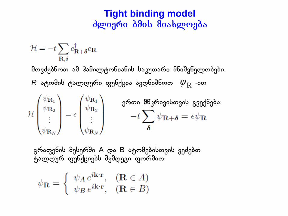
მოვძებნოთ ამ ჰამილტონიანის საკუთარი მნიშვნელობები.
R ატომის ტალღური ფუნქცია ავღნიშნოთ ψR -ით
ერთი მწკრივისთვის გვექნება:
გრაფენის მესერში A და BBატომებისთვის ვეძებთ ტალღურ ფუნქციებს შემდეგი ფორმით:
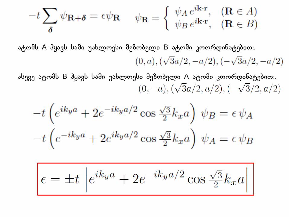
ატომს A ჰყავს სამი უახლოესი მეზობელი BBატომი კოორდინატებით:.
ასევე ატომს B ჰყავს სამი უახლოესი მეზობელი A ატომი კოორდინატებით:.
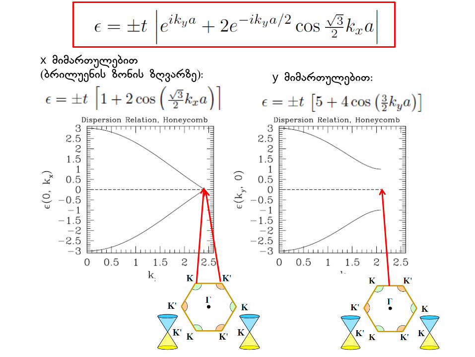
x მიმართულებით (ბრილუენის ზონის ზღვარზე): y მიმართულებით:
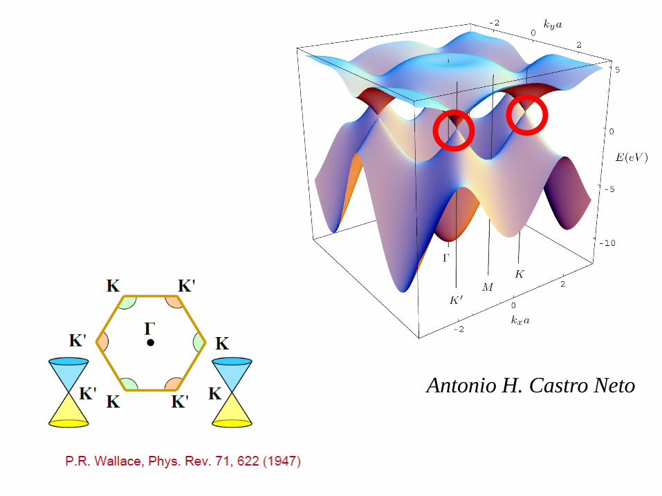
Antonio H. Castro Neto
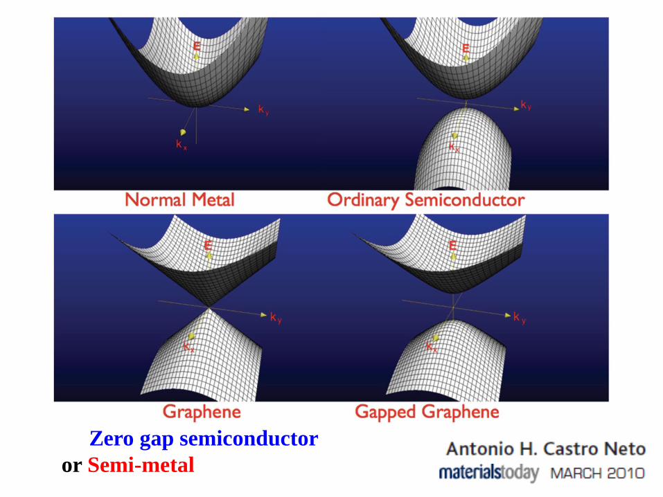
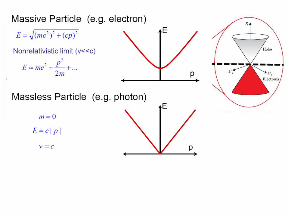
Zero gap semiconductor
or Semi-metal
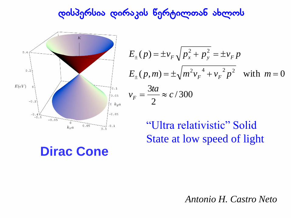
Dirac Cone
300/2
3
0 with ),(
)(
2242
22
cta
v
mpvvmmpE
pvppvpE
F
FF
FyxF
“Ultra relativistic” Solid
State at low speed of light
Antonio H. Castro Neto
დისპერსია დირაკის წერტილთან ახლოს
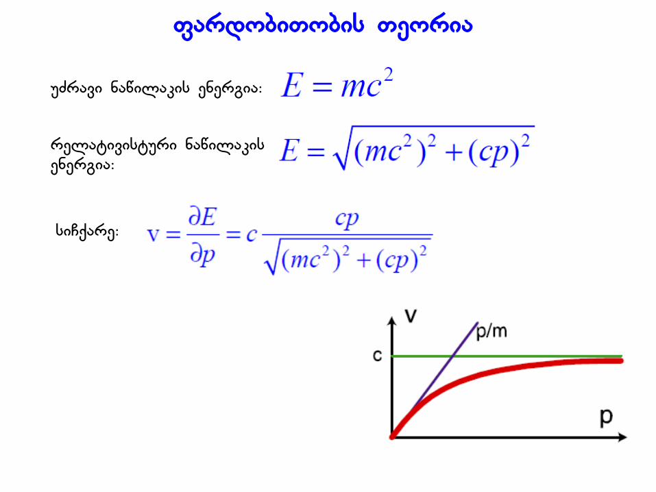
ფარდობითობის თეორია
უძრავი ნაწილაკის ენერგია:
რელატივისტური ნაწილაკის ენერგია:
სიჩქარე:
K
Ef
K K’
K’
Pz bonding
Valence band
Pz anti bonding
Conduction band
2DEG
Fermi energy
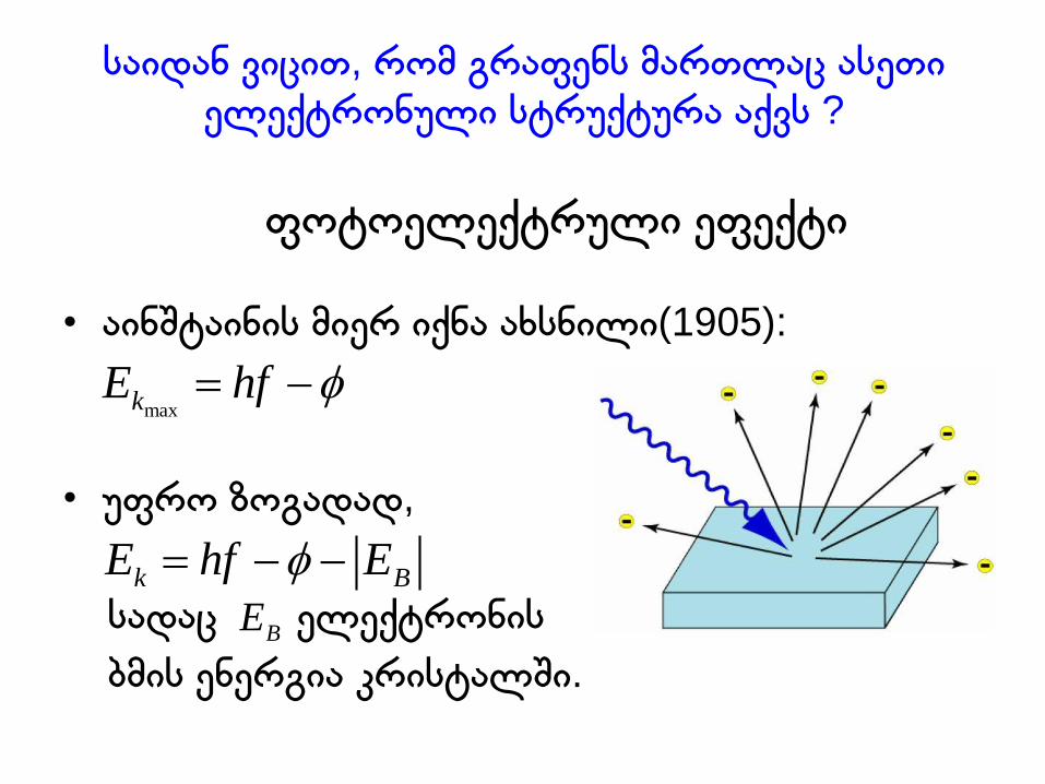
საიდან ვიცით, რომ გრაფენს მართლაც ასეთი ელექტრონული სტრუქტურა აქვს ?
ფოტოელექტრული ეფექტი
• აინშტაინის მიერ იქნა ახსნილი(1905):
• უფრო ზოგადად,
სადაც ელექტრონის
ბმის ენერგია კრისტალში.
maxkE hf
BEk BE hf E
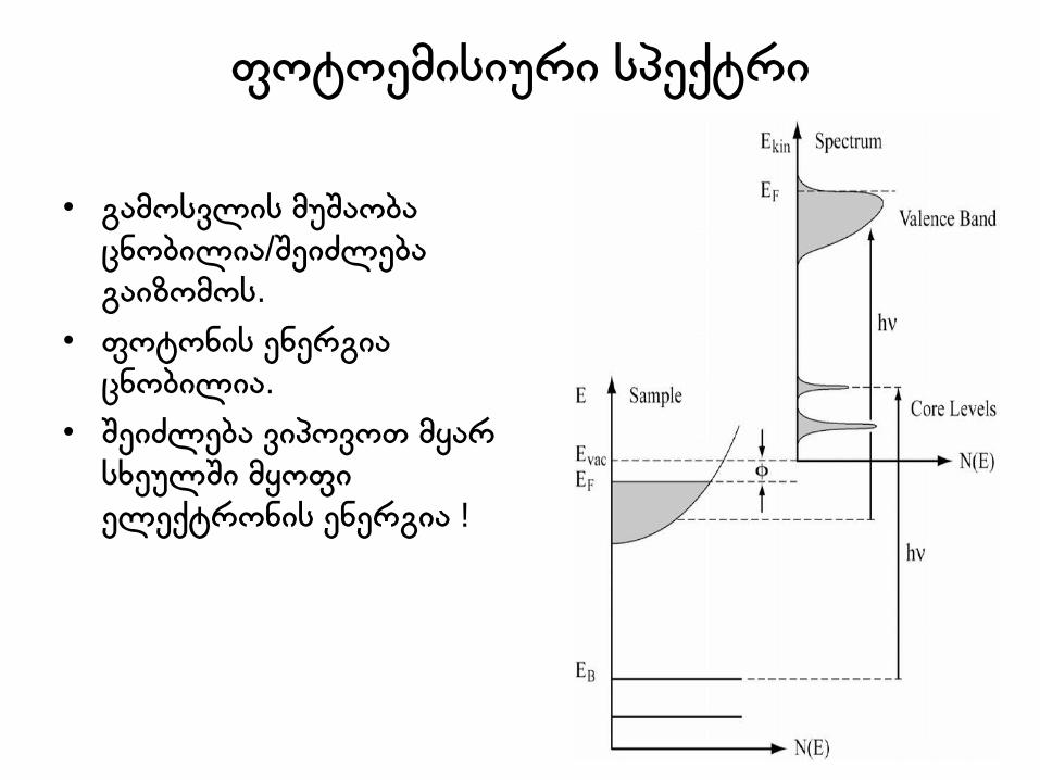
ფოტოემისიური სპექტრი
• გამოსვლის მუშაობა ცნობილია/შეიძლება გაიზომოს.
• ფოტონის ენერგია ცნობილია.
• შეიძლება ვიპოვოთ მყარ
სხეულში მყოფი ელექტრონის ენერგია !
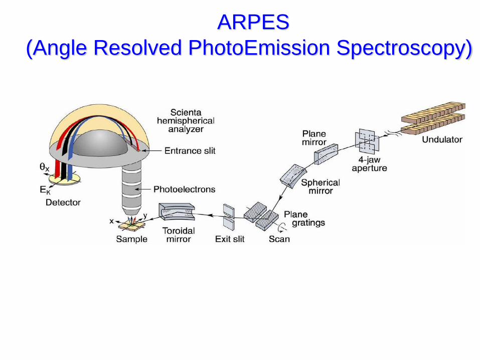
ARPES
(Angle Resolved PhotoEmission Spectroscopy)
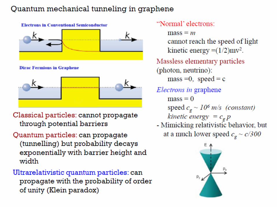
quantum-mechanical properties of the Dirac Hamiltonian
revealed a peculiar feature—Dirac carriers could not be
confined by electrostatic potentials (Klein, 1929).
An electron facing such a barrier would transmute into a
hole and propagate through the barrier.
There is no analog of this type of quantum-limited
transport regime in two-dimensional semiconductors.
Dirac Hamiltonian allows for both positive energy states (called
electrons) and negative energy states (called holes). While a
positive potential barrier is repulsive for electrons, it is
attractive for holes (and vice versa). For any potential barrier,
one needs to match the electron states outside the barrier with
the hole states inside the barrier. Since the larger the barrier
is, the greater the mode matching between electron and hole
states is, the transmission is also greater. For an infinite
barrier, the transmission becomes perfect. This is called
Klein tunneling (Klein, 1929).
graphene p-n junctions are essentially transparent.
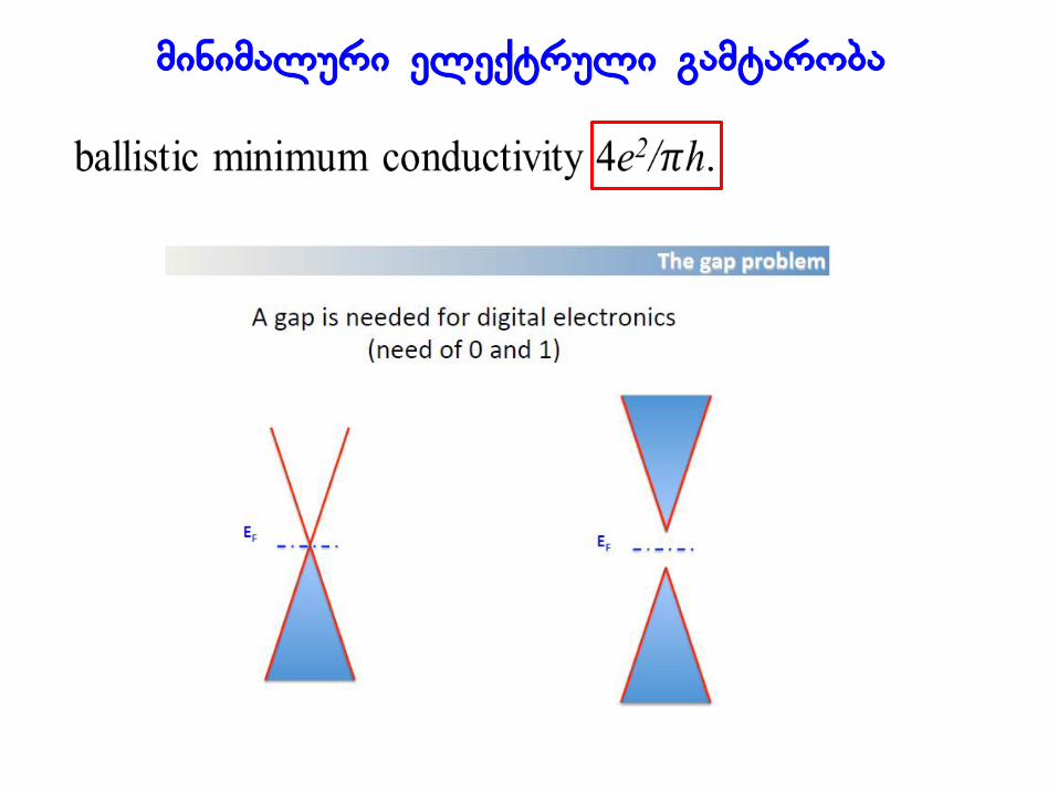
მინიმალური ელექტრული გამტარობა
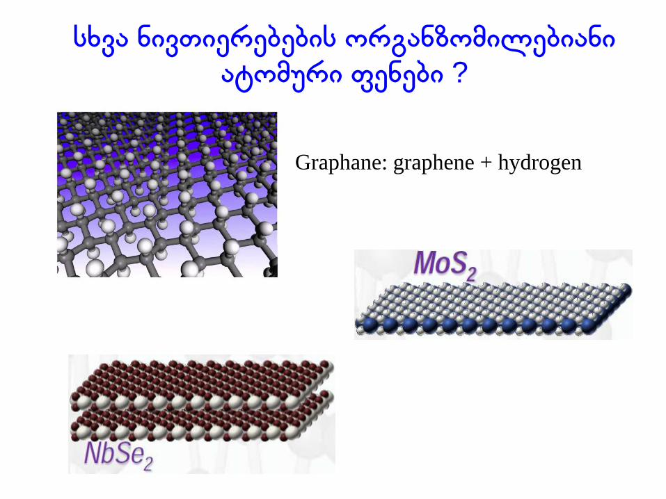
სხვა ნივთიერებების ორგანზომილებიანი ატომური ფენები ?
Graphane: graphene + hydrogen
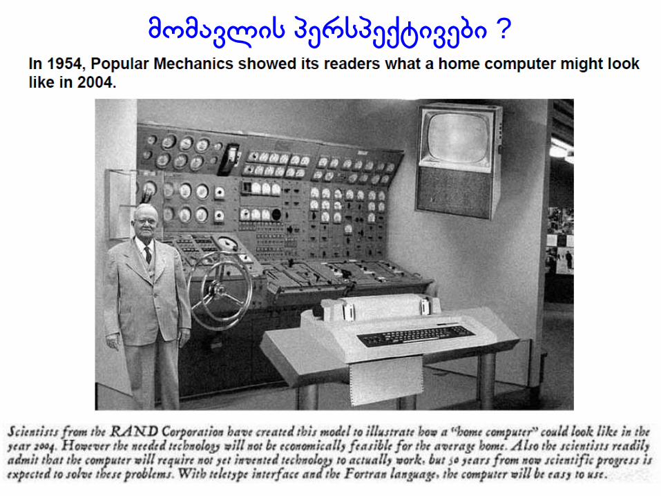
მომავლის პერსპექტივები ?