Embed Size (px)
Citation preview

TM
Freescale™ and the Freescale logo are trademarks of Freescale Semiconductor, Inc. All other product or service names are the property of their respective owners. © Freescale Semiconductor, Inc. 2006.
Freescale S12(X) MCU Seminar
Gareth Wang (王晓磊王晓磊王晓磊王晓磊)
FAE of Automotive Electronics
TMFreescale™ and the Freescale logo are trademarks of Freescale Semiconductor, Inc. All other product or service names are the property of their respective owners. © Freescale Semiconductor, Inc. 2006. 1
S12 (XE) Course AgendaS12 (XE) Course Agenda
Topic (AM 9:00~12:00)Topic (AM 9:00~12:00) DurationDuration PagePage
OverviewOverview S12(X) Overview 10 min 5
CoreCore Programming Model
Instruction Set
15 min 8
SystemSystem Interrupt Controller 15 min 7
Reset / Clocks / Low Power
20 min 7
Memory Map 25 min 23
Tea Break (10:25 ~ 10:35) 10 min
XGATEXGATE XGATE Brief 10 min 6
Programming Model
Instruction Set
10 min 9
XGATE Memory Map 5 min 4
XGATE Thread &
Configuration
25 min 16
XGATE SW Trigger &
Semaphore
15 min 7
S12XS & S12XS &
S12PS12PS12XS & S12P Brief 30 min 11
Topic (PM 13:00~17:00)Topic (PM 13:00~17:00) DurationDuration PagePage
Quick Quick
StartStart
LABsLABs
S12XEP100 Demo Board Brief
10 min 2
CodeWarrior 4.7
1st Simple Project
10 min 1
PeripheralPeripheral
LABsLABsE_EEPROM LAB 25 min 9
Memory Map LAB 25 min 5
MPU LAB (option) 20 min 6
Tea Break (14:30 ~ 14:40) 10 min
XGATEXGATE
LABsLABs
XGATE Configuration
(SCI demo)
20 min 2
PIT LABs 25 min 2
SW Trigger LABs 25 min 2
Tea Break (15:50 ~ 16:00) 10 min
GeneralGeneral
LABsLABs
Semaphore LABs 20 min 6
Virtual Peripheral
FullCan Driver (Demo)
20 min 14
Q&AQ&A Review and Q&A 15 min 1

TM
Freescale™ and the Freescale logo are trademarks of Freescale Semiconductor, Inc. All other product or service names are the property of their respective owners. © Freescale Semiconductor, Inc. 2006.
S12(X) Overview
TMFreescale™ and the Freescale logo are trademarks of Freescale Semiconductor, Inc. All other product or service names are the property of their respective owners. © Freescale Semiconductor, Inc. 2006. 3
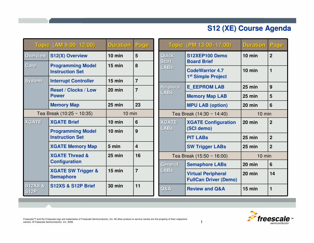
S12/S12X PPM Trend
0
1
2
3
4
5
J F M A M J J A S O N D J F M A M J J A S O N D J F M A M J J A S O N D
2006 2007 2008
FSL Assembly Date
PP
M
0
100
200
300
400
Cu
mu
lati
ve V
olu
me (
M)
PPM - 6 months rolling PPM - predicted Cumulative Volume (M)
S12(X): High Volume, High Quality
S12(X)
Now shipping
>100M# /yr!

TMFreescale™ and the Freescale logo are trademarks of Freescale Semiconductor, Inc. All other product or service names are the property of their respective owners. © Freescale Semiconductor, Inc. 2006. 444
16-bit Body Electronics MCU RoadmapA
pplic
ation P
erf
orm
ance / Inte
gra
tion
S12Q
32K
Lowest Cost8-16MHz
48,52,80pinROM Available
64K96K128K
S12C
32K
Low Cost16-25MHz
48,52,80pinROM Available
64K96K128K
32K
64K
128K S12PUltra Low Cost
LIN/CAN32Mhz
48,64,80 pin
64K
128K
256K S12XSReduced peripherals from S12XE
40MHz no XGATE, no MPU64, 80, 112pin
64K
128K
256KS12XD
40MHzXGATE
80,112,144 pin
512K
S12XBReduced peripheralsfrom S12XD 80,112pin
64K
128K
S12HZStepper Motor,
LCD Support25MHz
80,112 pin(ROM 32K-256K
512K
256K
S12XHStepper Motor,LCD Support
40MHz XGATE112,144 pin
512K
384K
256K
128K
S12XFFlexRay, XGATE, MPU, ECC
50MHz64,112pin
1M
768K
512K
384K
S12XE
XGATE, MPU, EEEPROM 50MHz
80,112,144,208pin
256K
128KS12ZG
512K
384K
S12GNext Gen Cost Reduction
16-240K FlashEEPROM
25MHz 20 TSSOP
32,48,64,100LQFP
256K
128K
384K
256K
S12XE Next GenCost Reduction
Linear CPUXGATE, MPU, EEPROM
60MHz 64,80,112 pin
S12(X)HY
32K
Stepper Motor, LCD Drive32MHz
64,100 pin
64K
48K
192K
2008 2009 2010 2011
128K
96K
64K
16K
32K
48K
240K
48K WindowLift
32K
128K
Application Specific High Integration µCSingle Die
Embedded LIN/CAN Phy40V Vreg
Application Specific Drivers32-64pin
128K
256K
Available
Planned
Proposed
In Design
96K
2012
TMFreescale™ and the Freescale logo are trademarks of Freescale Semiconductor, Inc. All other product or service names are the property of their respective owners. © Freescale Semiconductor, Inc. 2006. 5
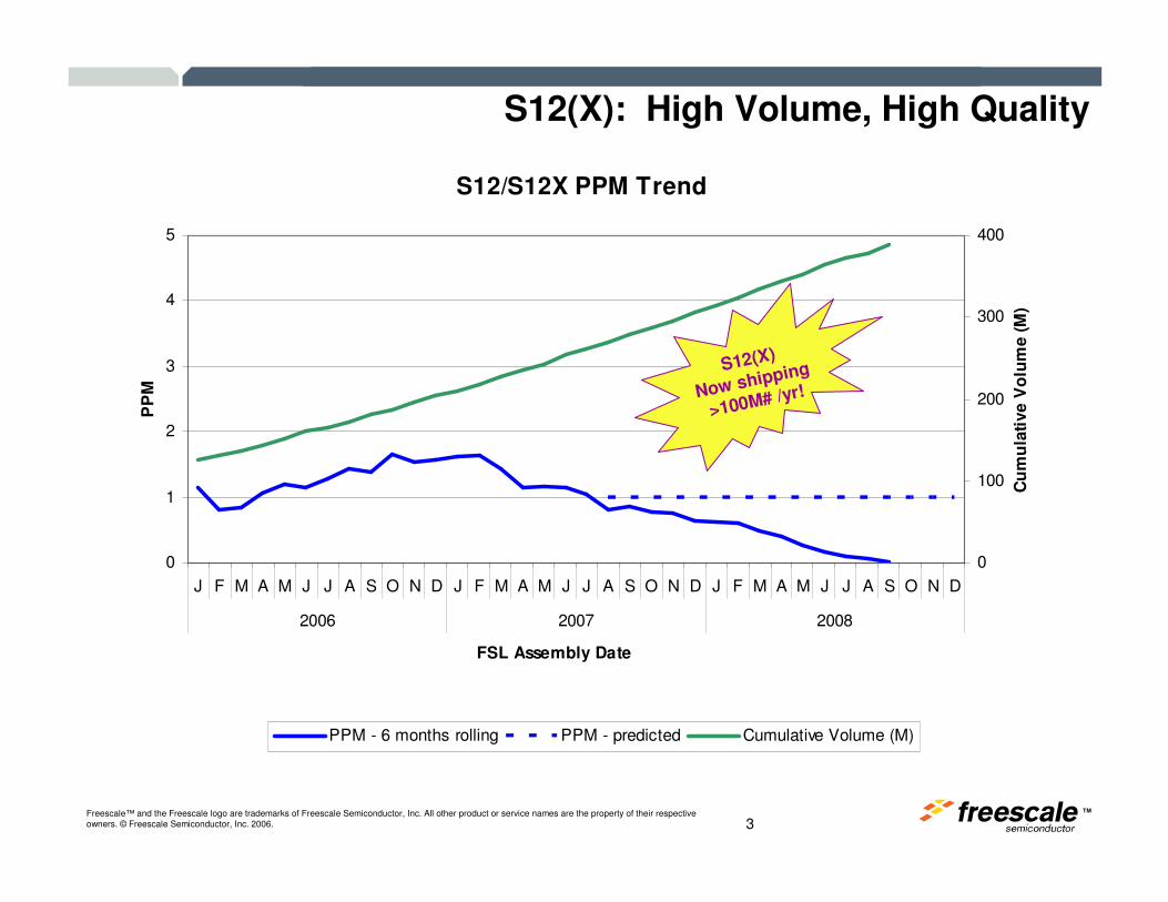
S12XE Family
This document contains forward-looking statements based on current expectations, forecast and assumptions of Freescale that involves risk and uncertainties. Forward looking statements are subject to risk and uncertainties associated with Freescale business that could cause actual results to vary materially from those stated or implied by such forward-looking statements.
Device Flash ROM RAM EE XGATE MPU EBI CAN
SCI
(LIN) SPI IIC ECT TIM PIT PWM ATD
Max
Speed
(MHz) Package9S12XEP100 1Mb 64 4 1 1 y 5 8 3 2 16b8ch 16b8ch 8ch 8b8c 32 50 112 LQFP 144QFP 208MBGA
9S12XEP768 768 48 4 1 1 y 5 8 3 2 16b8ch 16b8ch 8ch 8b8c 32 50 112 LQFP 144QFP 208MBGA
9S12XEQ512 512 32 4 1 1 y 4 6 3 2 16b8ch - 8ch 8b8c 24 50 80 QFP 112 LQFP 144QFP
9S12XEQ384 384 24 4 1 1 y 4 4 3 1 16b8ch - 4ch 8b8c 24 50 80QFP 112LQFP 144LQFP
9S12XET256 256 16 4 1 1 y 3 4 3 1 16b8ch - 4ch 8b8c 24 50 80QFP 112LQFP 144LQFP
9S12XEG128 128 12 2 1 1 y 2 2 2 1 16b8ch - 2ch 8b8c 16 50 80QFP 112LQFP
8 LIN/SCI
3 SPI
2 IIC
GPIO
FMPLL
5 MSCAN
ATD 12b 32ch
Timer 16b 8ch
ECT 16b 8ch
8ch PeriodicInterrupt Timer
PWM 8b 8ch
80/112/144QFP 208 MBGA
4KB EEPROM
MPU CRG
DBG INT
1MB Flash
64KB RAM
S12XCPU
External Bus Interface
Introducing the S12XE Family:
S12X CISC core @ 50MHzXGATE RISC core @ 100MHz
Enables higher system integrity at the ECU level (MPU, ECC, Supervisor Mode)
Improved EMI/EMCBetter resolution/faster ATD
Additional Periodic Interrupt Timer PIT
Enhanced XGATE now with interruptability
TMFreescale™ and the Freescale logo are trademarks of Freescale Semiconductor, Inc. All other product or service names are the property of their respective owners. © Freescale Semiconductor, Inc. 2006. 6
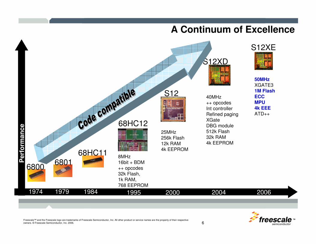
A Continuum of Excellence
6800
1974
6801
1979
68HC11
1984
68HC12
S12
S12XD
2000 20041995
8MHz16bit + BDM++ opcodes32k Flash, 1k RAM,768 EEPROM
25MHz256k Flash12k RAM4k EEPROM
40MHz++ opcodesInt controllerRefined pagingXGateDBG module512k Flash32k RAM4k EEPROM
S12XE
50MHzXGATE31M FlashECCMPU4k EEEATD++
2006
Perf
orm
an
ce
TMFreescale™ and the Freescale logo are trademarks of Freescale Semiconductor, Inc. All other product or service names are the property of their respective owners. © Freescale Semiconductor, Inc. 2006. 7
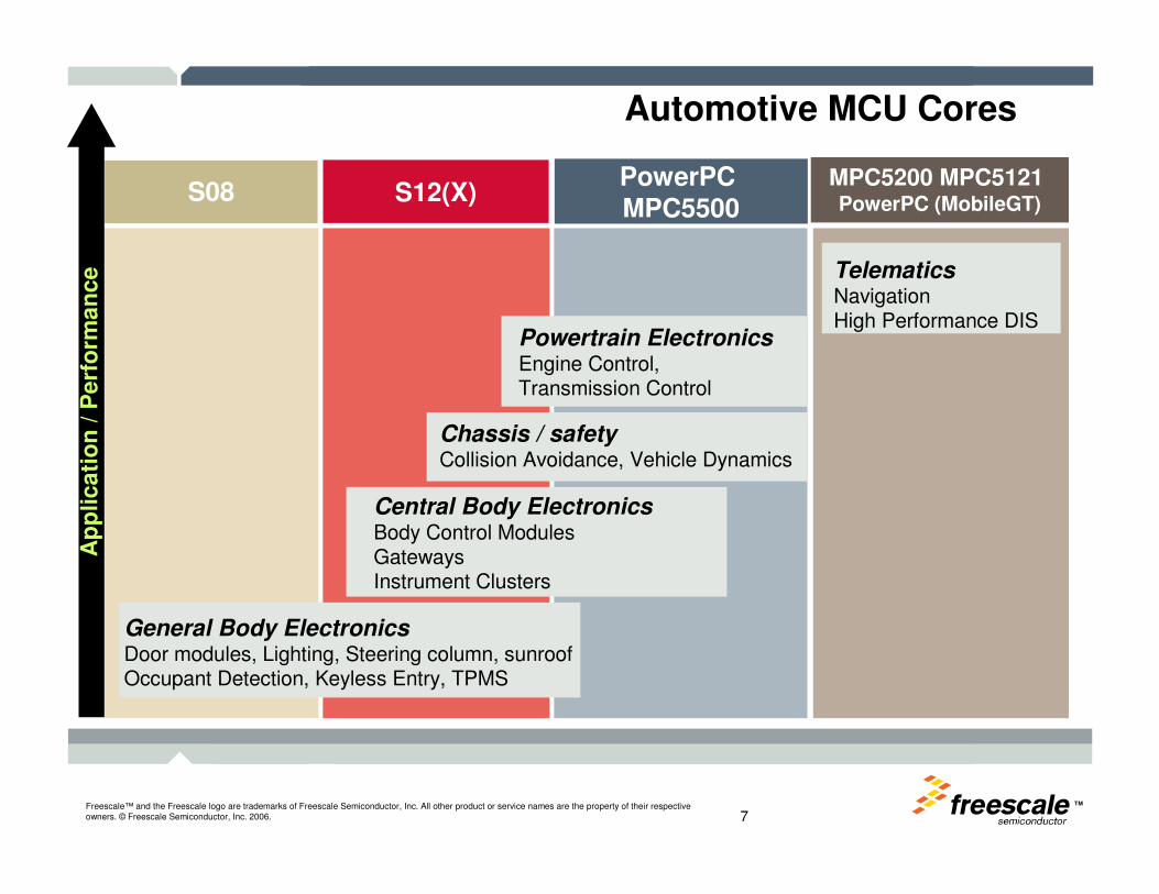
Automotive MCU Cores
MPC5200 MPC5121PowerPC (MobileGT)
PowerPC MPC5500
Powertrain ElectronicsEngine Control, Transmission Control
TelematicsNavigationHigh Performance DIS
Central Body ElectronicsBody Control ModulesGatewaysInstrument Clusters
General Body ElectronicsDoor modules, Lighting, Steering column, sunroofOccupant Detection, Keyless Entry, TPMS
S08
Chassis / safetyCollision Avoidance, Vehicle Dynamics
Ap
plica
tio
n /
Perf
orm
an
ce
S12(X)
TM
Freescale™ and the Freescale logo are trademarks of Freescale Semiconductor, Inc. All other product or service names are the property of their respective owners. © Freescale Semiconductor, Inc. 2006.
S12(X) Programming Model & Instruction Set
(S12CPU)
TMFreescale™ and the Freescale logo are trademarks of Freescale Semiconductor, Inc. All other product or service names are the property of their respective owners. © Freescale Semiconductor, Inc. 2006. 9
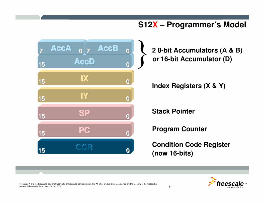
AccDAccDAccD
S12X – Programmer’s Model
AccAAccAAccA AccBAccBAccB
IXIXIX
IYIYIY
SPSPSP
PCPCPC
CCRCCRCCR
} 2 8-bit Accumulators (A & B)
or 16-bit Accumulator (D)000
000
000
000
000
000
000
151515
151515
151515
151515
151515
151515
777000777
Index Registers (X & Y)
Stack Pointer
Program Counter
Condition Code Register
(now 16-bits)
TMFreescale™ and the Freescale logo are trademarks of Freescale Semiconductor, Inc. All other product or service names are the property of their respective owners. © Freescale Semiconductor, Inc. 2006. 10
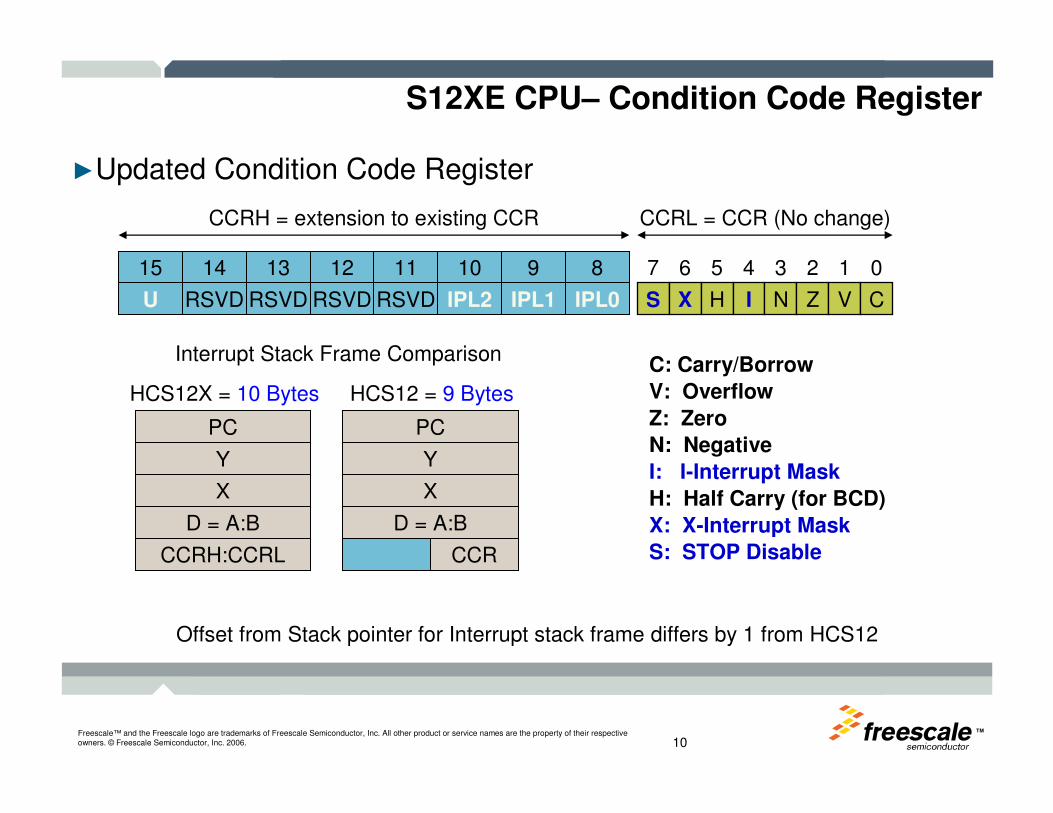
S12XE CPU– Condition Code Register
►Updated Condition Code Register
IPL2 IPL1 IPL0
8910
RSVD RSVD RSVD
111213
U RSVD
1415
S
7
X
6
H
5
I
4
N
3
Z
2
V
1
C
0
CCRL = CCR (No change)CCRH = extension to existing CCR
CCRH:CCRL
D = A:B
X
Y
PC
HCS12X = 10 Bytes HCS12 = 9 Bytes
Offset from Stack pointer for Interrupt stack frame differs by 1 from HCS12
Interrupt Stack Frame Comparison
CCR
D = A:B
X
Y
PC
C: Carry/Borrow
V: Overflow
Z: Zero
N: Negative
I: I-Interrupt Mask
H: Half Carry (for BCD)
X: X-Interrupt Mask
S: STOP Disable
TMFreescale™ and the Freescale logo are trademarks of Freescale Semiconductor, Inc. All other product or service names are the property of their respective owners. © Freescale Semiconductor, Inc. 2006. 11
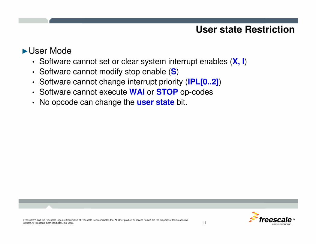
►User Mode• Software cannot set or clear system interrupt enables (X, I)
• Software cannot modify stop enable (S)
• Software cannot change interrupt priority (IPL[0..2])
• Software cannot execute WAI or STOP op-codes
• No opcode can change the user state bit.
User state Restriction

TMFreescale™ and the Freescale logo are trademarks of Freescale Semiconductor, Inc. All other product or service names are the property of their respective owners. © Freescale Semiconductor, Inc. 2006. 12
Addressing Modes
� INHERENT
� IMMEDIATE
� EXTENDED
� DIRECT
� INDEXED
INDEXED 5, 9 & 16 BIT OFFSET
INDEXED 16-BIT INDIRECT ([IDX2])
INDEXED AUTO PRE/POST DEC/INC
INDEXED ACCUMULATOR OFFSET
INDEXED D OFFSET-INDIRECT
([D,IDX])
� PC RELATIVE

TMFreescale™ and the Freescale logo are trademarks of Freescale Semiconductor, Inc. All other product or service names are the property of their respective owners. © Freescale Semiconductor, Inc. 2006. 13
Example: Indexed - Pre/Post Decrement/Increment
X2000
Y5 6 7 8
5 67 8
MOVW 2, X+ , 2,Y+
BEFORE
2002
AFTER
Y
X
3000 3002
AFTER
Other Examples:
MOVW 8,X+, 8,-Y
MOVW 2,X+ ,4,+Y
STAA 1, -SP
STAA 4, SP+
BEFORE
TMFreescale™ and the Freescale logo are trademarks of Freescale Semiconductor, Inc. All other product or service names are the property of their respective owners. © Freescale Semiconductor, Inc. 2006. 14
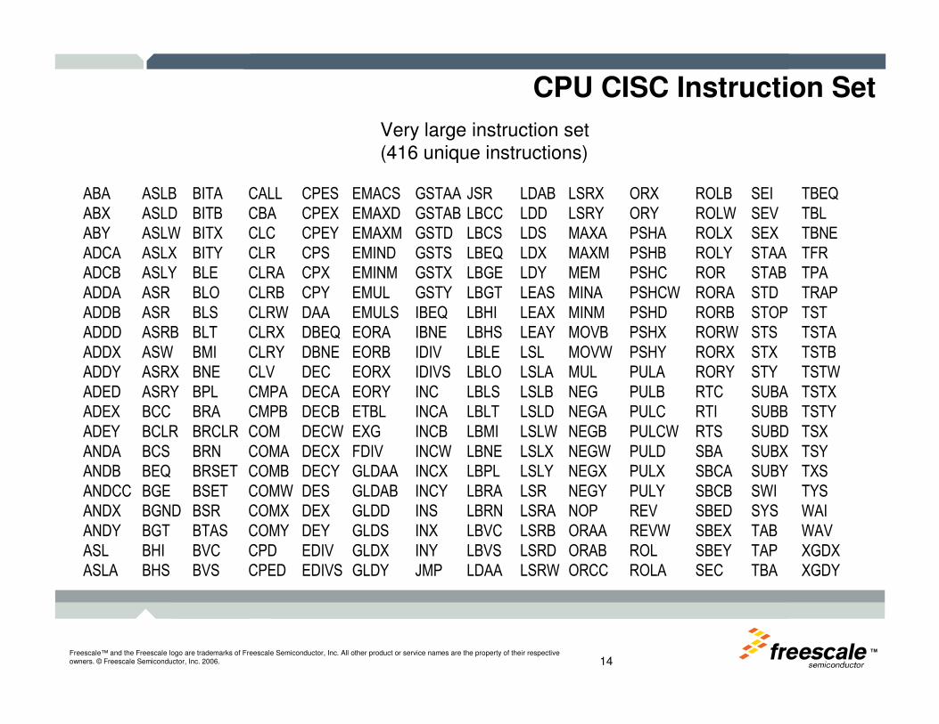
CPU CISC Instruction Set
Very large instruction set(416 unique instructions)
ABA
ABX
ABY
ADCA
ADCB
ADDA
ADDB
ADDD
ADDX
ADDY
ADED
ADEX
ADEY
ANDA
ANDB
ANDCC
ANDX
ANDY
ASL
ASLA
ASLB
ASLD
ASLW
ASLX
ASLY
ASR
ASR
ASRB
ASW
ASRX
ASRY
BCC
BCLR
BCS
BEQ
BGE
BGND
BGT
BHI
BHS
BITA
BITB
BITX
BITY
BLE
BLO
BLS
BLT
BMI
BNE
BPL
BRA
BRCLR
BRN
BRSET
BSET
BSR
BTAS
BVC
BVS
CALL
CBA
CLC
CLR
CLRA
CLRB
CLRW
CLRX
CLRY
CLV
CMPA
CMPB
COM
COMA
COMB
COMW
COMX
COMY
CPD
CPED
CPES
CPEX
CPEY
CPS
CPX
CPY
DAA
DBEQ
DBNE
DEC
DECA
DECB
DECW
DECX
DECY
DES
DEX
DEY
EDIV
EDIVS
EMACS
EMAXD
EMAXM
EMIND
EMINM
EMUL
EMULS
EORA
EORB
EORX
EORY
ETBL
EXG
FDIV
GLDAA
GLDAB
GLDD
GLDS
GLDX
GLDY
GSTAA
GSTAB
GSTD
GSTS
GSTX
GSTY
IBEQ
IBNE
IDIV
IDIVS
INC
INCA
INCB
INCW
INCX
INCY
INS
INX
INY
JMP
JSR
LBCC
LBCS
LBEQ
LBGE
LBGT
LBHI
LBHS
LBLE
LBLO
LBLS
LBLT
LBMI
LBNE
LBPL
LBRA
LBRN
LBVC
LBVS
LDAA
LDAB
LDD
LDS
LDX
LDY
LEAS
LEAX
LEAY
LSL
LSLA
LSLB
LSLD
LSLW
LSLX
LSLY
LSR
LSRA
LSRB
LSRD
LSRW
LSRX
LSRY
MAXA
MAXM
MEM
MINA
MINM
MOVB
MOVW
MUL
NEG
NEGA
NEGB
NEGW
NEGX
NEGY
NOP
ORAA
ORAB
ORCC
ORX
ORY
PSHA
PSHB
PSHC
PSHCW
PSHD
PSHX
PSHY
PULA
PULB
PULC
PULCW
PULD
PULX
PULY
REV
REVW
ROL
ROLA
ROLB
ROLW
ROLX
ROLY
ROR
RORA
RORB
RORW
RORX
RORY
RTC
RTI
RTS
SBA
SBCA
SBCB
SBED
SBEX
SBEY
SEC
SEI
SEV
SEX
STAA
STAB
STD
STOP
STS
STX
STY
SUBA
SUBB
SUBD
SUBX
SUBY
SWI
SYS
TAB
TAP
TBA
TBEQ
TBL
TBNE
TFR
TPA
TRAP
TST
TSTA
TSTB
TSTW
TSTX
TSTY
TSX
TSY
TXS
TYS
WAI
WAV
XGDX
XGDY
TMFreescale™ and the Freescale logo are trademarks of Freescale Semiconductor, Inc. All other product or service names are the property of their respective owners. © Freescale Semiconductor, Inc. 2006. 15
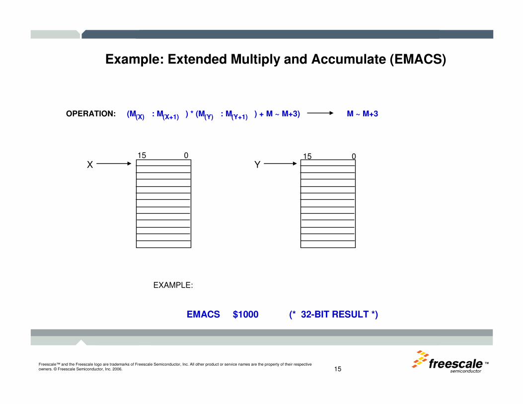
Example: Extended Multiply and Accumulate (EMACS)
OPERATION: (M : M ) * (M : M ) + M ~ M+3) M ~ M+3(X) (X+1) (Y) (Y+1)
X Y
EXAMPLE:
EMACS $1000 (* 32-BIT RESULT *)
15 0 15 0

TMFreescale™ and the Freescale logo are trademarks of Freescale Semiconductor, Inc. All other product or service names are the property of their respective owners. © Freescale Semiconductor, Inc. 2006. 16
►New 16-Bit Read-Modify-Write Instructions• complementing the 8 Bit counterparts using same addressing
modes:INCW,DECW,NEGW,LSRW,ROLW,RORW,ASRW,ASLW,CLRW
►X, Y can also act as 16Bit Accumulators
►Logical and arithmetic instructions can also operate on X, Y registers
S12X Instruction Set Enhancements
TM
Freescale™ and the Freescale logo are trademarks of Freescale Semiconductor, Inc. All other product or service names are the property of their respective owners. © Freescale Semiconductor, Inc. 2006.
Interrupt Controller

TMFreescale™ and the Freescale logo are trademarks of Freescale Semiconductor, Inc. All other product or service names are the property of their respective owners. © Freescale Semiconductor, Inc. 2006. 18
S12XCPU Interrupt Flow
Continue Main Program
Software Interrupt Hardware Interrupt
Mask Set?
Stack MCU Register Contents
Set I Bit in CCR
Load Interrupt Vector Into
Program Counter
Execute Interrupt Service Routine
Vector
Table
$FF80
$FFFF
YN
Default
S
7
X
6
H
5
I4
N
3
Z
2
V
1
C
0
TMFreescale™ and the Freescale logo are trademarks of Freescale Semiconductor, Inc. All other product or service names are the property of their respective owners. © Freescale Semiconductor, Inc. 2006. 19
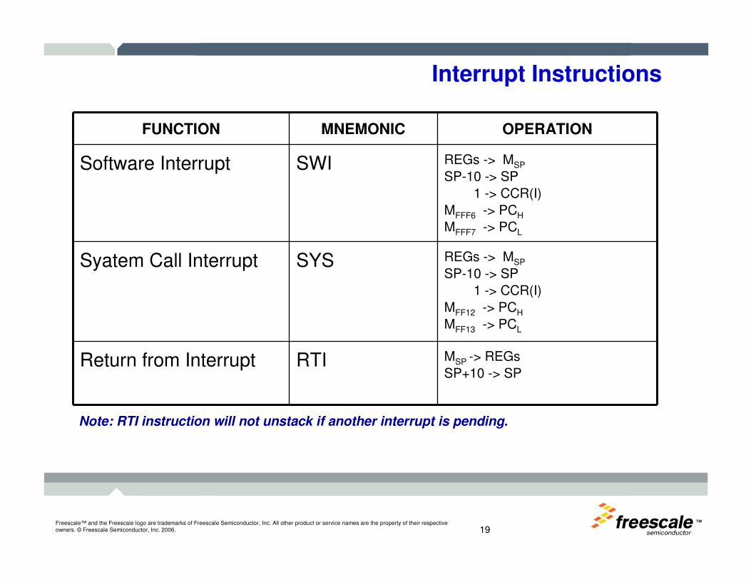
Interrupt Instructions
Note: RTI instruction will not unstack if another interrupt is pending.
FUNCTION MNEMONIC OPERATION
Software Interrupt SWI REGs -> MSP
SP-10 -> SP
1 -> CCR(I)
MFFF6 -> PCH
MFFF7 -> PCL
Syatem Call Interrupt SYS REGs -> MSP
SP-10 -> SP
1 -> CCR(I)
MFF12 -> PCH
MFF13 -> PCL
Return from Interrupt RTI MSP -> REGs
SP+10 -> SP

TMFreescale™ and the Freescale logo are trademarks of Freescale Semiconductor, Inc. All other product or service names are the property of their respective owners. © Freescale Semiconductor, Inc. 2006. 20
Interrupt Stacking Order
When S12XCPU acknowledges an interrupt, it stacks registers, then determines which vector to take.
SP before operation
SP after operation
XX_XX
PC
Y
X
D
CCRSP-10
SP-8
SP-6
SP-4
SP-2
SP

TMFreescale™ and the Freescale logo are trademarks of Freescale Semiconductor, Inc. All other product or service names are the property of their respective owners. © Freescale Semiconductor, Inc. 2006. 21
Interrupt Module Architecture (CPU view)
Cro
ss b
ar
sw
itch
Up to 1
17
Incom
ing Inte
rrupt
Req
uests
Inte
rrup
t V
ecto
r B
ase R
egis
ter
16
8
8
VectorAddress
Lower Address Bits
Upper Address Bits
Priority Decoder
7
Priority Decoder
2
Priority Decoder
1
Disabled0
TopLevel Decoder
Winnerof the
Winners
TMFreescale™ and the Freescale logo are trademarks of Freescale Semiconductor, Inc. All other product or service names are the property of their respective owners. © Freescale Semiconductor, Inc. 2006. 22
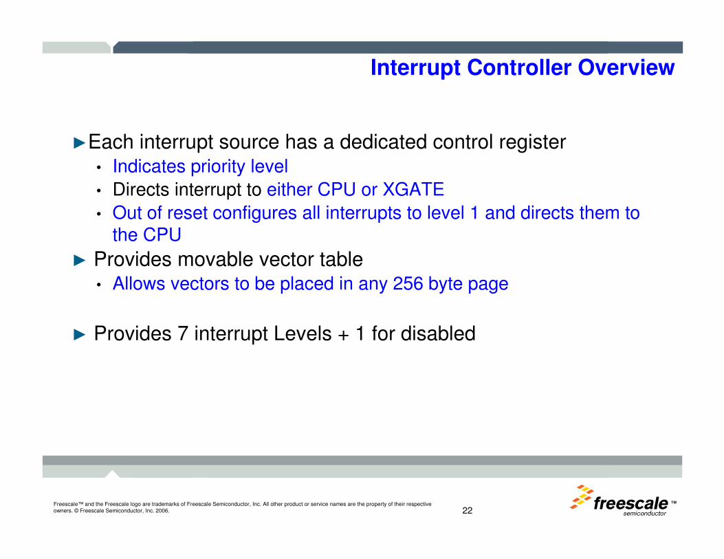
Interrupt Controller Overview
►Each interrupt source has a dedicated control register• Indicates priority level
• Directs interrupt to either CPU or XGATE
• Out of reset configures all interrupts to level 1 and directs them to the CPU
► Provides movable vector table• Allows vectors to be placed in any 256 byte page
► Provides 7 interrupt Levels + 1 for disabled

TMFreescale™ and the Freescale logo are trademarks of Freescale Semiconductor, Inc. All other product or service names are the property of their respective owners. © Freescale Semiconductor, Inc. 2006. 23
Interrupt Controller Example
XXX
0XX
30X
0XX
0XX
0XX
XXX
0 3 7 3 2 1 0
Resume 3
7 interrupts 3
2 higher than pending 1
RTI
0
234
1
567
Pro
cessin
g L
evel
RTIRTI
* IPL[2:0] is stored on the stack with the new high byte of the CCR
IPL*
TMFreescale™ and the Freescale logo are trademarks of Freescale Semiconductor, Inc. All other product or service names are the property of their respective owners. © Freescale Semiconductor, Inc. 2006. 24
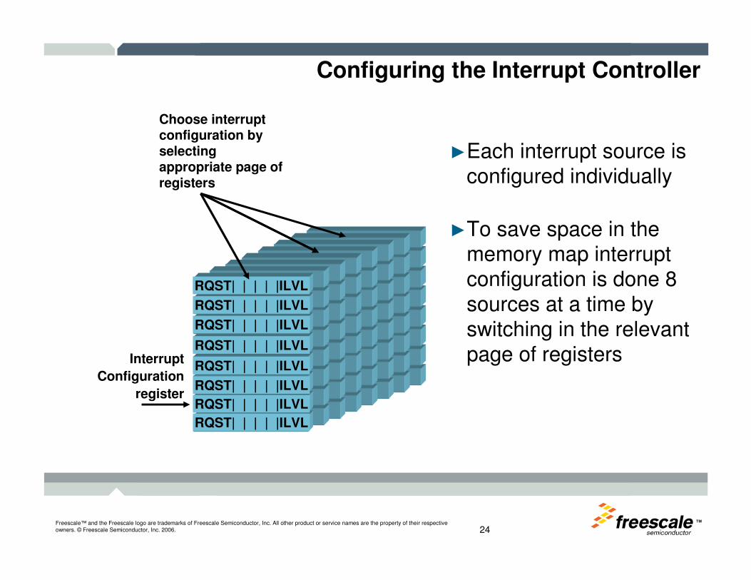
Configuring the Interrupt Controller
►Each interrupt source is configured individually
►To save space in the memory map interrupt configuration is done 8 sources at a time by switching in the relevant page of registers
RQST| | | | |ILVL
RQST| | | | |ILVL
RQST| | | | |ILVL
RQST| | | | |ILVL
RQST| | | | |ILVL
RQST| | | | |ILVL
RQST| | | | |ILVL
RQST| | | | |ILVL
Interrupt
Configuration
register
Choose interrupt configuration by selecting appropriate page of registers
TM
Freescale™ and the Freescale logo are trademarks of Freescale Semiconductor, Inc. All other product or service names are the property of their respective owners. © Freescale Semiconductor, Inc. 2006.
Reset / Clock / Low Power

TMFreescale™ and the Freescale logo are trademarks of Freescale Semiconductor, Inc. All other product or service names are the property of their respective owners. © Freescale Semiconductor, Inc. 2006. 26
RESETS
Reset Sources
� Power-On Reset (POR) None None
� Low Voltage Reset (LVR) None None
� External pin RESET None None
� Illegal Address Reset None None
� Clock monitor reset
� COP watchdog reset
TMFreescale™ and the Freescale logo are trademarks of Freescale Semiconductor, Inc. All other product or service names are the property of their respective owners. © Freescale Semiconductor, Inc. 2006. 27
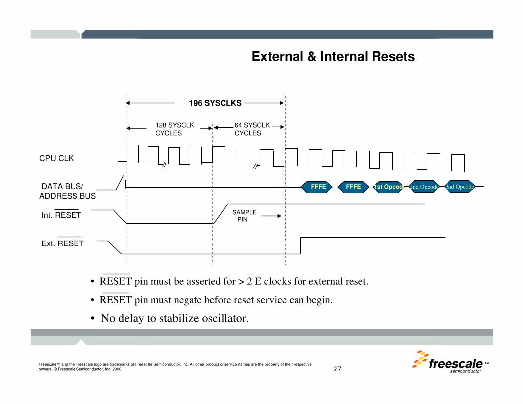
External & Internal Resets
• RESET pin must be asserted for > 2 E clocks for external reset.
• RESET pin must negate before reset service can begin.
• No delay to stabilize oscillator.
128 SYSCLKCYCLES
64 SYSCLKCYCLES
CPU CLK
DATA BUS/ADDRESS BUS
Int. RESET
Ext. RESET
196 SYSCLKS
SAMPLEPIN
FFFE FFFE 1st Opcode 2nd Opcode 3nd Opcode
TMFreescale™ and the Freescale logo are trademarks of Freescale Semiconductor, Inc. All other product or service names are the property of their respective owners. © Freescale Semiconductor, Inc. 2006. 28
BUS CLOCK
OSC CLOCKCRG
CORE CLOCK = 2 x BUSCLK
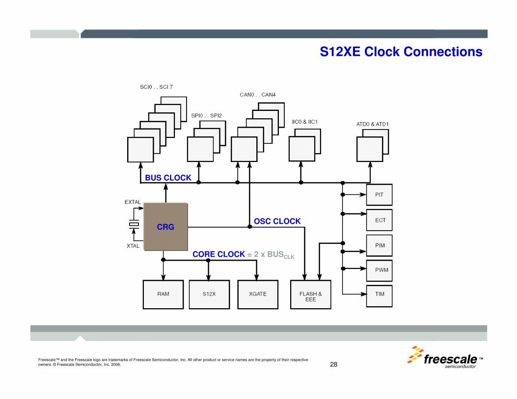
S12XE Clock Connections
TMFreescale™ and the Freescale logo are trademarks of Freescale Semiconductor, Inc. All other product or service names are the property of their respective owners. © Freescale Semiconductor, Inc. 2006. 29
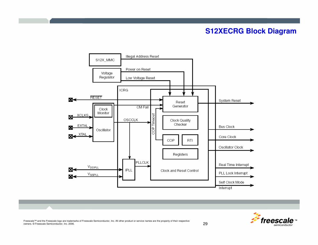
S12XECRG Block Diagram

TMFreescale™ and the Freescale logo are trademarks of Freescale Semiconductor, Inc. All other product or service names are the property of their respective owners. © Freescale Semiconductor, Inc. 2006. 30
Clock Quality Check
► The Clock Quality is checked to determine if the crystal is suitable to run from
when:
• POR (power-on-reset) occurs
• Exiting STOP mode
• After Clock Monitor failure
► A Quality Check Window is 50K SCM (Self-Clock-Mode) cycles, which are the
PLL min. freq. (1 to 5.5 Mhz)
► To satisfy the Clock Quality Check, 4096 osclk cycles must occur within a
Quality Check Window. The 4096 counter is reset at the end of each window,
hence all 4096 must occur within the same window.
► When the Quality Check is satisfied, the MCU exits reset after 192 sysclk
cycles.
► If the Quality Check is NOT satisfied after 50 Check Windows, the MCU exits
reset in SCM (Self-Clock-Mode).

TMFreescale™ and the Freescale logo are trademarks of Freescale Semiconductor, Inc. All other product or service names are the property of their respective owners. © Freescale Semiconductor, Inc. 2006. 31
Computer Operating Properly (1 of 3)
Useful for: 1. Insuring that the MCU does not get "hung up"
for an extended period of time.
2. Improves fault tolerance of system.
Description: If the COP rate select bits are not “0” and if the watchdog timer
is not reset within a specified time period:
1. Then a system reset is asserted on the external reset pin.
2. COP vector is fetched ( $FFFA-$FFFB )
Pins: 1. Reset - Asserted for 128 clocks.

TMFreescale™ and the Freescale logo are trademarks of Freescale Semiconductor, Inc. All other product or service names are the property of their respective owners. © Freescale Semiconductor, Inc. 2006. 32
Computer Operating Properly (2 of 3)
PINS 1. RESET Asserted for 128 clocks
ARMCOP - CRG COP Arm/Reset Timer
– Software writes $55 followed by $AA to ARMCOP, to reset internal COP counter.
Address Offset$000E
Address Offset$0008
WCOP - Window COP Mode1 = Window COP operation (Writes to ARMCOP Register must occur in the last 25% of selected period).0 = Normal COP operation
CR[2:0] - COP Watchdog Timer Rate SelectCOPCTL : Write Once in user mode, anytime in test mode.
A write to COPCTL will initialize COP counter .
COPCTL - CRG COP Control Register
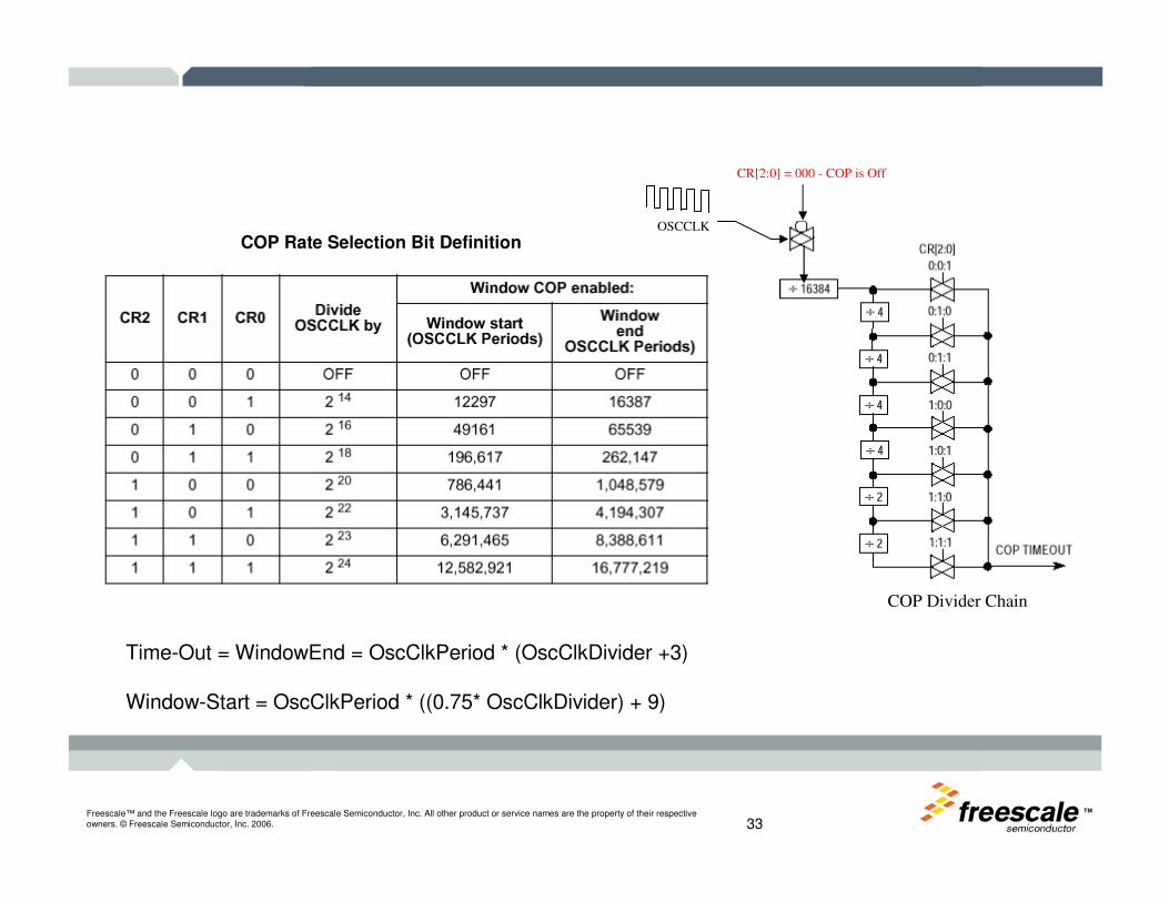
TMFreescale™ and the Freescale logo are trademarks of Freescale Semiconductor, Inc. All other product or service names are the property of their respective owners. © Freescale Semiconductor, Inc. 2006. 33
COP Time-out Period Select (3 OF 3)
COP Rate Selection Bit Definition
Time-Out = WindowEnd = OscClkPeriod * (OscClkDivider +3)
Window-Start = OscClkPeriod * ((0.75* OscClkDivider) + 9)
CR[2:0] = 000 - COP is Off
OSCCLK
COP Divider Chain
TMFreescale™ and the Freescale logo are trademarks of Freescale Semiconductor, Inc. All other product or service names are the property of their respective owners. © Freescale Semiconductor, Inc. 2006. 34
Fast Wake-up from Full STOP
►In full STOP mode the crystal oscillator is stopped• Minimum current usage
• Disadvantage of delay required to restart crystal oscillations
►S12X provides the option of overcoming the disadvantage with thecrystal start up
• Fast wake up (FSTWKP) bit forces the self-clock mode to become active
• This provides ~2.5MHz (unreferenced) VCO clock which is sufficient for non time-critical functions
• The VCO is the oscillator of the PLL
TMFreescale™ and the Freescale logo are trademarks of Freescale Semiconductor, Inc. All other product or service names are the property of their respective owners. © Freescale Semiconductor, Inc. 2006. 35
Low Power Modes
Full Stop Mode*� Oscillator is stopped in this mode; � All clocks are switched off by default;� All counters and dividers remain frozen by default; � The Autonomous Periodic Interrupt (API) and ATD modules may be enabled to self
wake the device;� A Fast wake up mode is available.
Pseudo Stop Mode*� System clocks are stopped but the oscillator still run; � RTI, COP, API and ATD modules may be enabled; � Other peripherals are turned off. � Consumes more current than system stop mode;� Full speed wake up time from this mode is significantly shorter than STOP mode.
*Entered when the CPU executes the STOP instruction. (Supervisor mode and CCR[S] cleared)
Wait Mode� Entered when the CPU executes the WAI instruction; � The internal CPU clock is switched off; � All peripherals and the XGATE can be active;� Peripherals can individually turn off their local clocks. � Asserting RESET, XIRQ, IRQ or any other interrupt that is not masked and is not routed
to XGATE ends system wait mode.
TMFreescale™ and the Freescale logo are trademarks of Freescale Semiconductor, Inc. All other product or service names are the property of their respective owners. © Freescale Semiconductor, Inc. 2006. 36
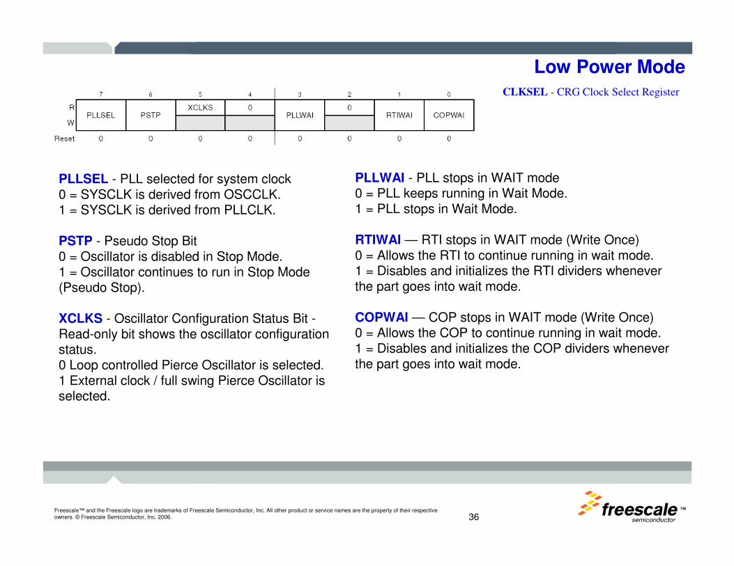
Low Power ModeCLKSEL - CRG Clock Select Register
PLLSEL - PLL selected for system clock0 = SYSCLK is derived from OSCCLK.1 = SYSCLK is derived from PLLCLK.
PSTP - Pseudo Stop Bit0 = Oscillator is disabled in Stop Mode.1 = Oscillator continues to run in Stop Mode (Pseudo Stop).
XCLKS - Oscillator Configuration Status Bit -Read-only bit shows the oscillator configuration status.0 Loop controlled Pierce Oscillator is selected.1 External clock / full swing Pierce Oscillator is selected.
PLLWAI - PLL stops in WAIT mode0 = PLL keeps running in Wait Mode.1 = PLL stops in Wait Mode.
RTIWAI — RTI stops in WAIT mode (Write Once)0 = Allows the RTI to continue running in wait mode.1 = Disables and initializes the RTI dividers whenever the part goes into wait mode.
COPWAI — COP stops in WAIT mode (Write Once)0 = Allows the COP to continue running in wait mode.1 = Disables and initializes the COP dividers whenever the part goes into wait mode.
TM
Freescale™ and the Freescale logo are trademarks of Freescale Semiconductor, Inc. All other product or service names are the property of their respective owners. © Freescale Semiconductor, Inc. 2006.
S12XCPU Memory Map
TMFreescale™ and the Freescale logo are trademarks of Freescale Semiconductor, Inc. All other product or service names are the property of their respective owners. © Freescale Semiconductor, Inc. 2006. 38
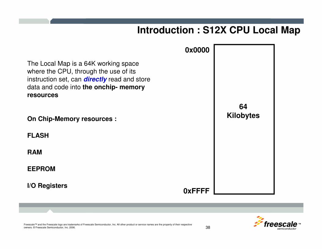
Introduction : S12X CPU Local Map
The Local Map is a 64K working space where the CPU, through the use of its instruction set, can directly read and store data and code into the onchip- memory resources
On Chip-Memory resources :
FLASH
RAM
EEPROM
I/O Registers
0x0000
0xFFFF
64 Kilobytes
TMFreescale™ and the Freescale logo are trademarks of Freescale Semiconductor, Inc. All other product or service names are the property of their respective owners. © Freescale Semiconductor, Inc. 2006. 39
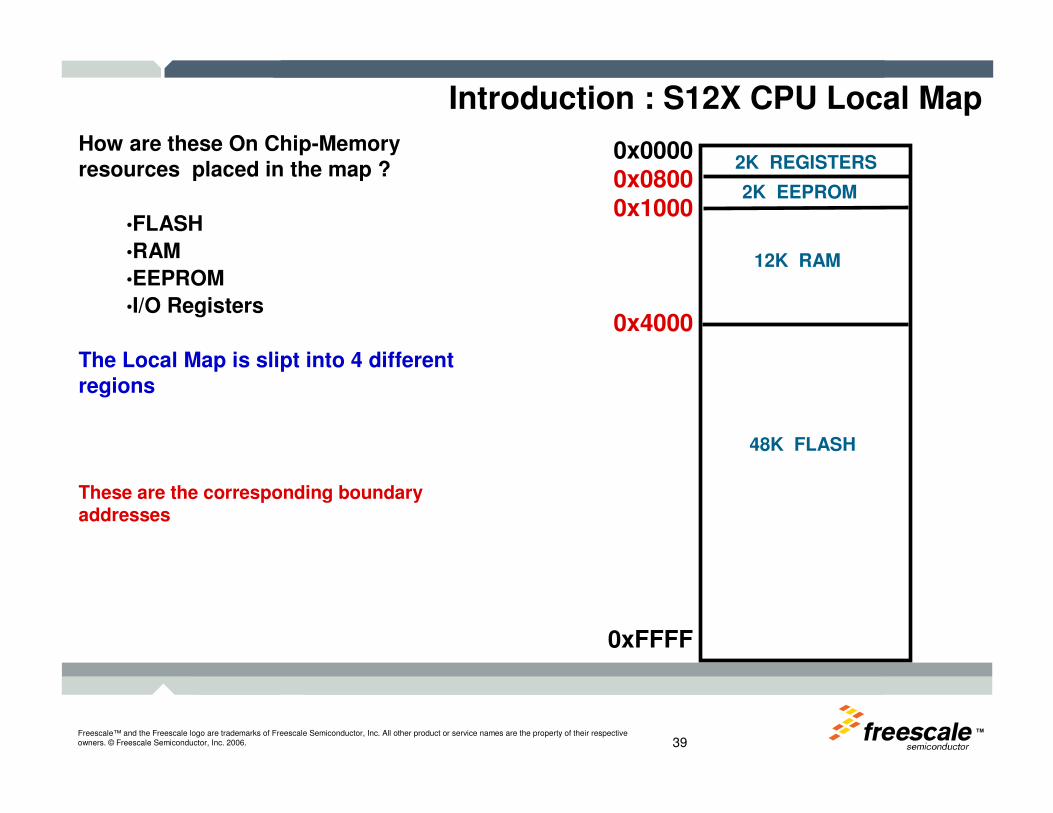
Introduction : S12X CPU Local Map
How are these On Chip-Memory resources placed in the map ?
•FLASH
•RAM
•EEPROM
•I/O Registers
The Local Map is slipt into 4 different regions
These are the corresponding boundary addresses
0x00000x08000x1000
0x4000
0xFFFF
2K EEPROM
2K REGISTERS
12K RAM
48K FLASH
TMFreescale™ and the Freescale logo are trademarks of Freescale Semiconductor, Inc. All other product or service names are the property of their respective owners. © Freescale Semiconductor, Inc. 2006. 40
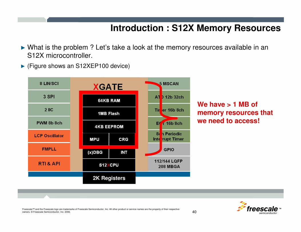
Introduction : S12X Memory Resources
► What is the problem ? Let’s take a look at the memory resources available in an S12X microcontroller.
► (Figure shows an S12XEP100 device)
We have > 1 MB of memory resources that we need to access!
2K Registers
TMFreescale™ and the Freescale logo are trademarks of Freescale Semiconductor, Inc. All other product or service names are the property of their respective owners. © Freescale Semiconductor, Inc. 2006. 41
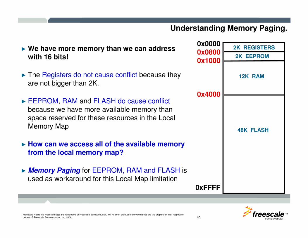
Understanding Memory Paging.
► We have more memory than we can address with 16 bits!
► The Registers do not cause conflict because they are not bigger than 2K.
► EEPROM, RAM and FLASH do cause conflictbecause we have more available memory than space reserved for these resources in the Local Memory Map
► How can we access all of the available memory from the local memory map?
► Memory Paging for EEPROM, RAM and FLASH is used as workaround for this Local Map limitation
0x00000x08000x1000
0x4000
0xFFFF
2K EEPROM
2K REGISTERS
12K RAM
48K FLASH
TMFreescale™ and the Freescale logo are trademarks of Freescale Semiconductor, Inc. All other product or service names are the property of their respective owners. © Freescale Semiconductor, Inc. 2006. 42
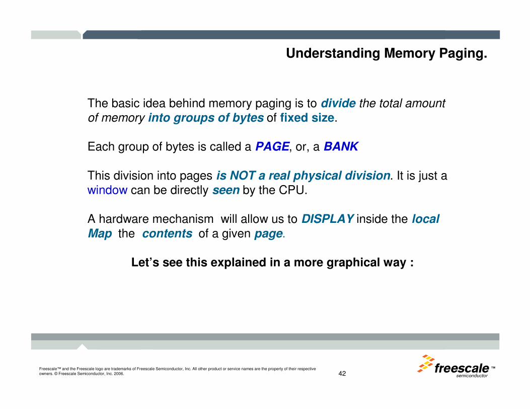
Understanding Memory Paging.
The basic idea behind memory paging is to divide the total amount
of memory into groups of bytes of fixed size.
Each group of bytes is called a PAGE, or, a BANK
This division into pages is NOT a real physical division. It is just a window can be directly seen by the CPU.
A hardware mechanism will allow us to DISPLAY inside the local
Map the contents of a given page.
Let’s see this explained in a more graphical way :
TMFreescale™ and the Freescale logo are trademarks of Freescale Semiconductor, Inc. All other product or service names are the property of their respective owners. © Freescale Semiconductor, Inc. 2006. 43
2K EEPROM
2K REGISTERS
12K RAM
48K FLASH
0x00000x0800
0x1000
0x4000
0xFFFF
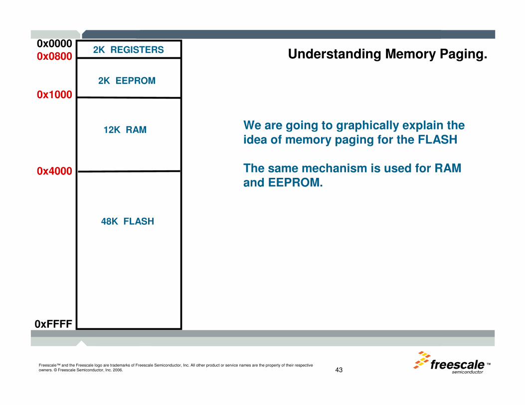
We are going to graphically explain the idea of memory paging for the FLASH
The same mechanism is used for RAM and EEPROM.
Understanding Memory Paging.
TMFreescale™ and the Freescale logo are trademarks of Freescale Semiconductor, Inc. All other product or service names are the property of their respective owners. © Freescale Semiconductor, Inc. 2006. 44
2K EEPROM
2K REGISTERS
12K RAM
48K FLASH
0x00000x0800
0x1000
0x4000
0x8000
0xC000
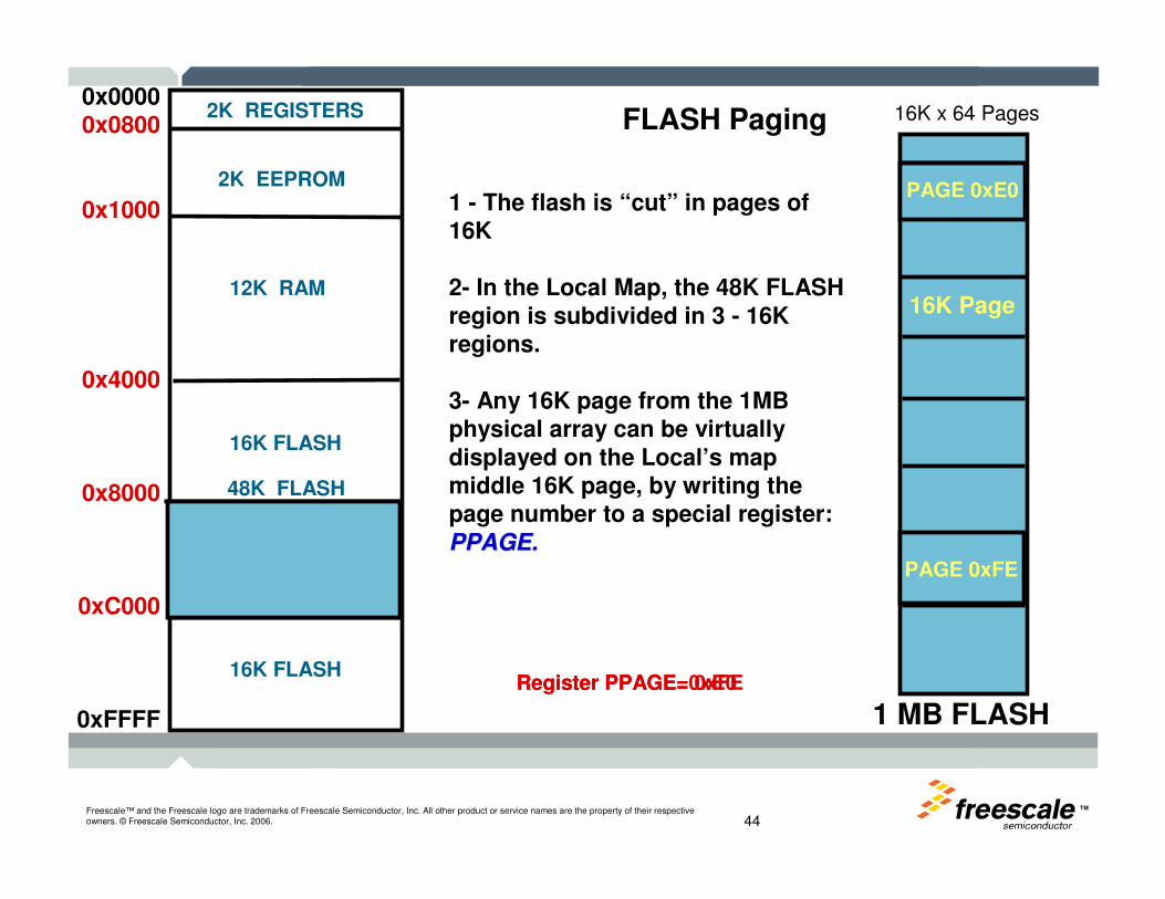
0xFFFF 1 MB FLASH
1 - The flash is “cut” in pages of 16K
2- In the Local Map, the 48K FLASH region is subdivided in 3 - 16K regions.
3- Any 16K page from the 1MB physical array can be virtually displayed on the Local’s map middle 16K page, by writing the page number to a special register:
PPAGE.PPAGE.
16K FLASH
16K FLASH
16K FLASH
PAGE 0xFE
Register PPAGE= 0xFE
16K Page
PAGE 0xE0
Register PPAGE=0xE0
FLASH Paging 16K x 64 Pages
TMFreescale™ and the Freescale logo are trademarks of Freescale Semiconductor, Inc. All other product or service names are the property of their respective owners. © Freescale Semiconductor, Inc. 2006. 45
4K EEPROM
1K Page2K EEPROM
2K REGISTERS
12K RAM
0x00000x08000x0C00
0x1000
0x4000
0x8000
0xC000
0xFFFF
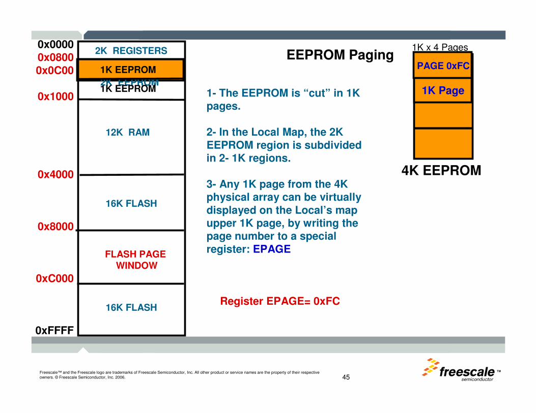
1- The EEPROM is “cut” in 1K pages.
2- In the Local Map, the 2K EEPROM region is subdivided in 2- 1K regions.
3- Any 1K page from the 4K physical array can be virtually displayed on the Local’s map upper 1K page, by writing the page number to a special register: EPAGE
16K FLASH
FLASH PAGE WINDOW
16K FLASHRegister EPAGE= 0xFC
PAGE 0xFCEEPROM Paging
1K EEPROM
1K EEPROM
1K x 4 Pages
TMFreescale™ and the Freescale logo are trademarks of Freescale Semiconductor, Inc. All other product or service names are the property of their respective owners. © Freescale Semiconductor, Inc. 2006. 46
2K REGISTERS
12K RAM
0x00000x08000x0C00
0x1000
0x2000
0x4000
0x8000
0xC000
0xFFFF
16K FLASH
FLASH PAGE WINDOW
16K FLASH
1K EEPROM
EEPROM WINDOW
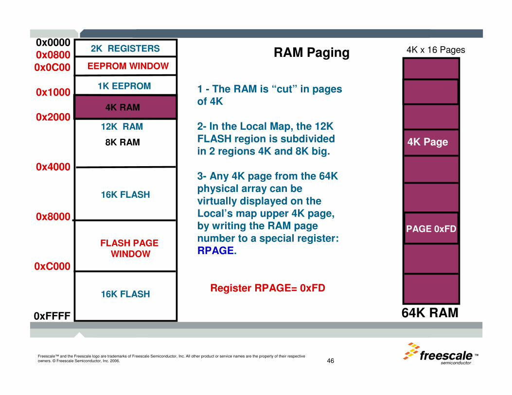
1 - The RAM is “cut” in pages of 4K
2- In the Local Map, the 12K FLASH region is subdivided in 2 regions 4K and 8K big.
3- Any 4K page from the 64K physical array can be virtually displayed on the Local’s map upper 4K page, by writing the RAM page number to a special register: RPAGE.
64K RAM
4K Page
PAGE 0xFD
8K RAM
4K RAM
Register RPAGE= 0xFD
RAM Paging 4K x 16 Pages

TMFreescale™ and the Freescale logo are trademarks of Freescale Semiconductor, Inc. All other product or service names are the property of their respective owners. © Freescale Semiconductor, Inc. 2006. 47
2K REGISTERS0x00000x08000x0C00
0x1000
0x2000
0x4000
0x8000
0xC000
0xFFFF
16K FLASH
FLASH PAGE WINDOW
16K FLASH
1K EEPROM
1K EEPROM WINDOW
8K RAM
4K RAM WINDOW
Q: What about the other memory regions in the local map ?
A : They are mapped to FIXEDlocations on the physical memory. The physical addresses that are mapped here are defined at chip
integration level.
Because you do not need to handle a PAGE register to access this memory, these
regions are called UNPAGEDor UNBANKED

TMFreescale™ and the Freescale logo are trademarks of Freescale Semiconductor, Inc. All other product or service names are the property of their respective owners. © Freescale Semiconductor, Inc. 2006. 48
Paging Mechanism
► Paging Mechanism: We have seen how to make it work. Now let’s see what’s behind this.
EPAGE
RPAGE
PPAGE
ALL Available Physical Memory
Local Memory Map Memory Mapping Control Module(MMC)
TMFreescale™ and the Freescale logo are trademarks of Freescale Semiconductor, Inc. All other product or service names are the property of their respective owners. © Freescale Semiconductor, Inc. 2006. 49
The Global Map
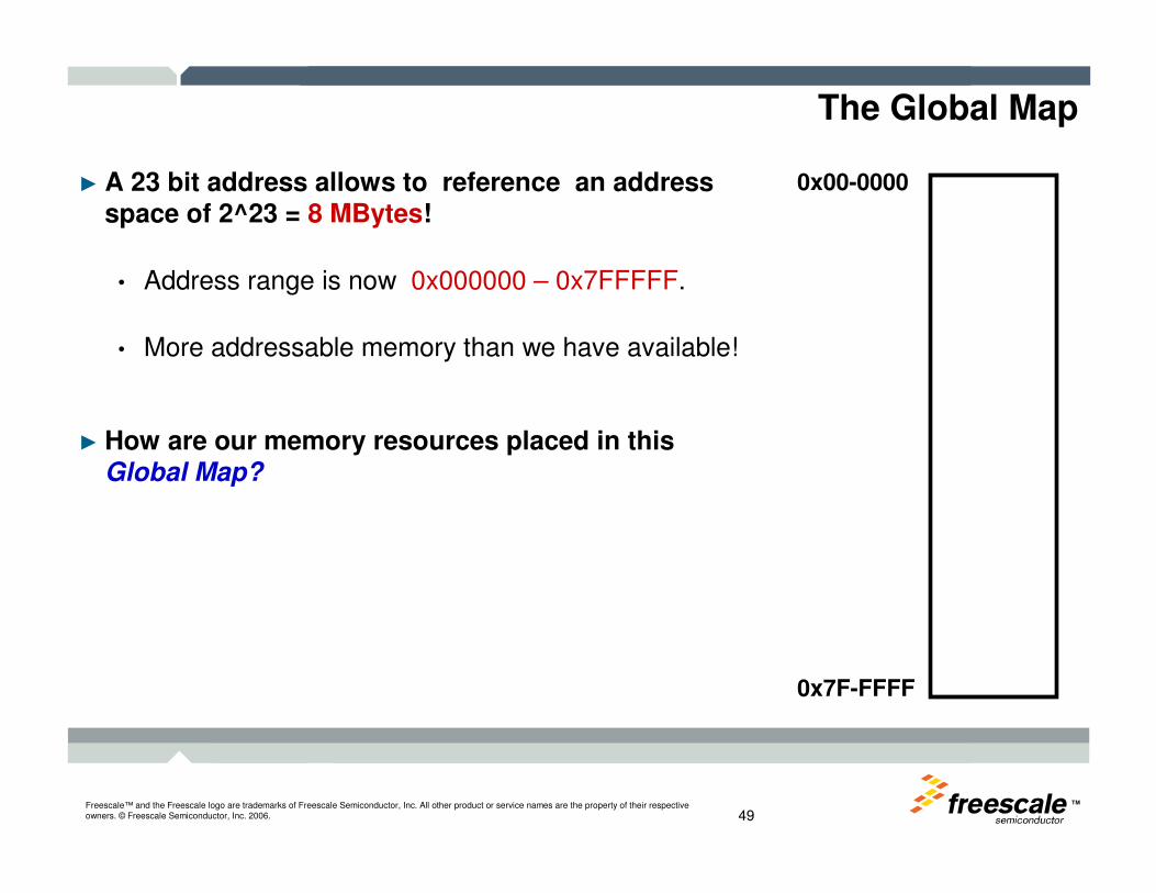
► A 23 bit address allows to reference an address space of 2^23 = 8 MBytes!
• Address range is now 0x000000 – 0x7FFFFF.
• More addressable memory than we have available!
► How are our memory resources placed in this Global Map?
0x00-0000
0x7F-FFFF
TMFreescale™ and the Freescale logo are trademarks of Freescale Semiconductor, Inc. All other product or service names are the property of their respective owners. © Freescale Semiconductor, Inc. 2006. 50
How are our memory resources placed in this Global Map
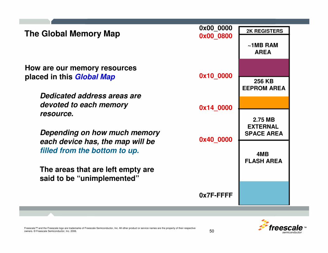
Dedicated address areas are devoted to each memory resource.
Depending on how much memory each device has, the map will be filled from the bottom to up.
The areas that are left empty are said to be “unimplemented”
4MB FLASH AREA
256 KBEEPROM AREA
~1MB RAMAREA
2.75 MBEXTERNAL
SPACE AREA
2K REGISTERS0x00_00000x00_0800
0x10_0000
0x14_0000
0x40_0000
0x7F-FFFF
The Global Memory Map
TMFreescale™ and the Freescale logo are trademarks of Freescale Semiconductor, Inc. All other product or service names are the property of their respective owners. © Freescale Semiconductor, Inc. 2006. 51
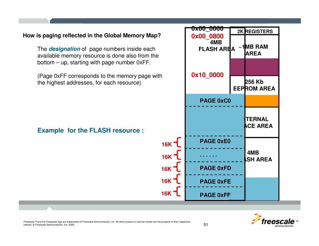
How is paging reflected in the Global Memory Map?
The designation of page numbers inside each available memory resource is done also from the bottom – up, starting with page number 0xFF.
(Page 0xFF corresponds to the memory page with the highest addresses, for each resource)
Example for the FLASH resource :
4MB FLASH AREA
256 KbEEPROM AREA
~1MB RAMAREA
EXTERNAL SPACE AREA
2K REGISTERS0x00_00000x00_0800
0x10_0000
0x14_0000
0x40_0000
0x7F-FFFF
4MB FLASH AREA
PAGE 0xC0
PAGE 0xE0
. . . . . .
PAGE 0xFD
PAGE 0xFE
PAGE 0xFF
16K
16K
16K
16K
16K

TMFreescale™ and the Freescale logo are trademarks of Freescale Semiconductor, Inc. All other product or service names are the property of their respective owners. © Freescale Semiconductor, Inc. 2006. 52
Local map (for reference)2K REGISTERS0x00000x0800
0x0BFF0x0C000x1000
0x1FFF0x2000
0x4000
0x8000
0xBFFF0xC000
0xFFFF
16K FLASH
FLASH PAGE WINDOW
16K FLASH
1K EEPROM
1K EEPROM WINDOW
8K RAM
4K RAM WINDOW EEPROM WINDOW Addresses : 0x0800-0x0BFF
RAM WINDOW Addresses: 0x1000-0x1FFF
FLASH WINDOW Adresses: 0x8000-0xBFFF
TMFreescale™ and the Freescale logo are trademarks of Freescale Semiconductor, Inc. All other product or service names are the property of their respective owners. © Freescale Semiconductor, Inc. 2006. 53
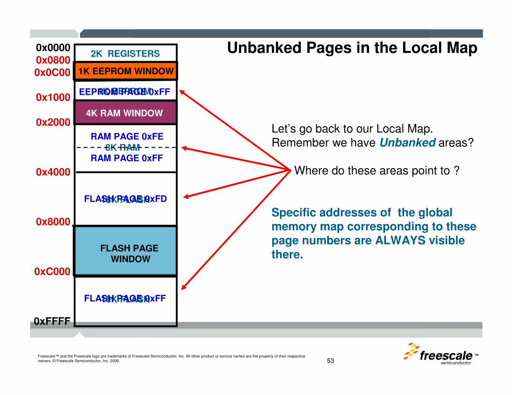
Unbanked Pages in the Local Map2K REGISTERS0x00000x08000x0C00
0x1000
0x2000
0x4000
0x8000
0xC000
0xFFFF
16K FLASH
FLASH PAGE WINDOW
16K FLASH
1K EEPROM
1K EEPROM WINDOW
8K RAM
4K RAM WINDOW
Let’s go back to our Local Map. Remember we have Unbanked areas?
Where do these areas point to ?
Specific addresses of the global memory map corresponding to these page numbers are ALWAYS visible there.
RAM PAGE 0xFE
RAM PAGE 0xFF
FLASH PAGE 0xFD
FLASH PAGE 0xFF
EEPROM PAGE 0xFF
TMFreescale™ and the Freescale logo are trademarks of Freescale Semiconductor, Inc. All other product or service names are the property of their respective owners. © Freescale Semiconductor, Inc. 2006. 54
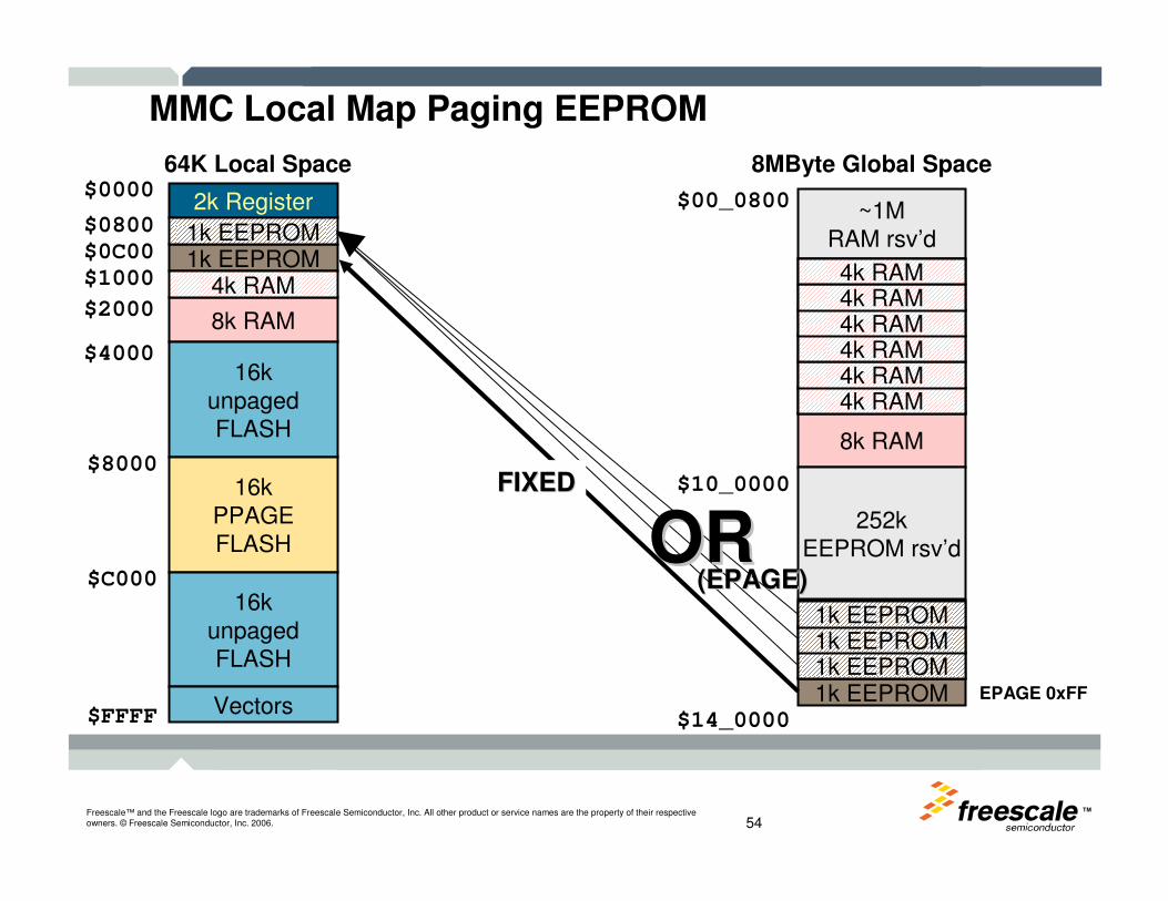
MMC Local Map Paging EEPROM
2k Register
1k EEPROM
$0000
8k RAM
$0800
$1000
16kunpagedFLASH
$4000
16kPPAGEFLASH
16kunpagedFLASH
$8000
$C000
Vectors$FFFF
64K Local Space 8MByte Global Space
$10_0000
~1MRAM rsv’d
8k RAM
252kEEPROM rsv’d
1k EEPROM$14_0000
$00_0800
4k RAM$2000
1k EEPROM$0C00
4k RAM4k RAM4k RAM4k RAM4k RAM4k RAM
1k EEPROM1k EEPROM1k EEPROM
OROR(EPAGE)(EPAGE)
FIXEDFIXED
EPAGE 0xFF

TMFreescale™ and the Freescale logo are trademarks of Freescale Semiconductor, Inc. All other product or service names are the property of their respective owners. © Freescale Semiconductor, Inc. 2006. 55
MMC Local Map Paging RAM (e.g., S12XE device)
2k Register
1k EEPROM
$0000
8k RAM
$0800
$1000
16kunpagedFLASH
$4000
16kPPAGEFLASH
16kunpagedFLASH
$8000
$C000
Vectors$FFFF
64K Local Space 8MByte Global Space
$10_0000
~1MRAM rsv’d
8k RAM
252kEEPROM rsv’d
1k EEPROM$14_0000
$00_0800
4k RAM$2000
1k EEPROM$0C00
4k RAM4k RAM4k RAM4k RAM4k RAM4k RAM
1k EEPROM1k EEPROM1k EEPROM
OROR(RPAGE)(RPAGE)
FIXEDFIXED
RPAGE 0xFERPAGE 0xFF
TMFreescale™ and the Freescale logo are trademarks of Freescale Semiconductor, Inc. All other product or service names are the property of their respective owners. © Freescale Semiconductor, Inc. 2006. 56
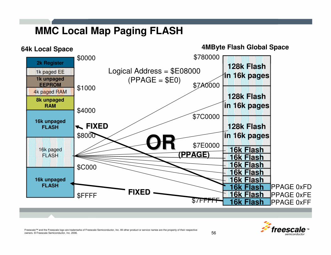
MMC Local Map Paging FLASH
16k Flash
4MByte Flash Global Space
$7E0000
16k Flash$7FFFFF
$780000
16k Flash16k Flash16k Flash
64k Local Space
$00002k Register
1k unpagedEEPROM
8k unpagedRAM
4k paged RAM
1k paged EE
16k unpagedFLASH
16k pagedFLASH
16k unpagedFLASH
$1000
$4000
$8000
$C000
$FFFF
16k Flash16k Flash16k Flash16k Flash
128k Flashin 16k pages
128k Flashin 16k pages
128k Flashin 16k pages
OROR(PPAGE)(PPAGE)
FIXEDFIXED
$7C0000
$7A0000
Logical Address = $E08000(PPAGE = $E0)
PPAGE 0xFDPPAGE 0xFEPPAGE 0xFF
FIXEDFIXED

TMFreescale™ and the Freescale logo are trademarks of Freescale Semiconductor, Inc. All other product or service names are the property of their respective owners. © Freescale Semiconductor, Inc. 2006. 57
Logical Address Concept
16Bit Local Address
16Bit Local Address8Bit Page Register
8Bit Page Register
Logical addresses are used in link parameters (prm file)
TMFreescale™ and the Freescale logo are trademarks of Freescale Semiconductor, Inc. All other product or service names are the property of their respective owners. © Freescale Semiconductor, Inc. 2006. 58
Paging mechanism Conclusions
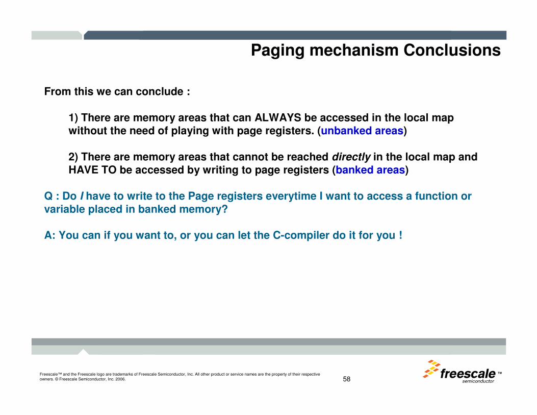
From this we can conclude :
1) There are memory areas that can ALWAYS be accessed in the local map without the need of playing with page registers. (unbanked areas)
2) There are memory areas that cannot be reached directly in the local map andHAVE TO be accessed by writing to page registers (banked areas)
Q : Do I have to write to the Page registers everytime I want to access a function or variable placed in banked memory?
A: You can if you want to, or you can let the C-compiler do it for you !
OK, so, how do I make this work by using CodeWarrior ?
TMFreescale™ and the Freescale logo are trademarks of Freescale Semiconductor, Inc. All other product or service names are the property of their respective owners. © Freescale Semiconductor, Inc. 2006. 59
4MB FLASH AREA
256 KbEEPROM AREA
~1MB RAMAREA
EXTERNAL SPACE AREA
2K REGISTERS
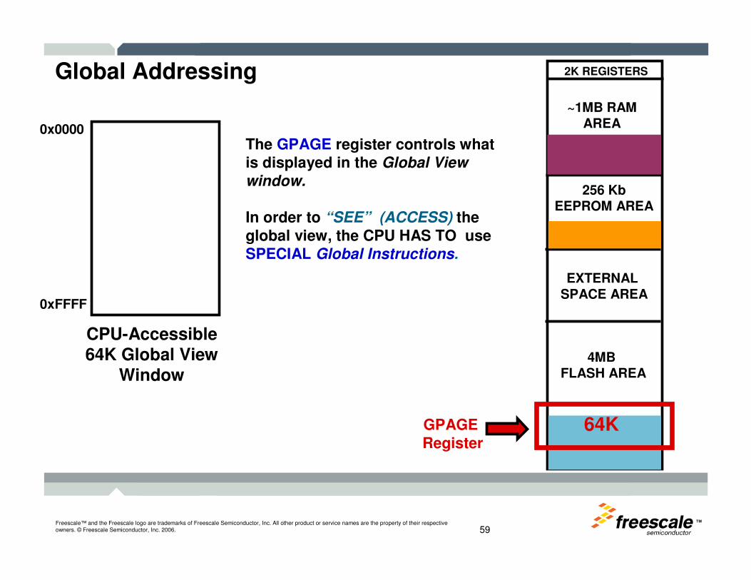
CPU-Accessible 64K Global View
Window
0x0000
0xFFFF
The GPAGE register controls what is displayed in the Global View
window.
In order to “SEE” (ACCESS) the global view, the CPU HAS TO use SPECIAL Global Instructions.
GPAGERegister
64K
Global Addressing
TMFreescale™ and the Freescale logo are trademarks of Freescale Semiconductor, Inc. All other product or service names are the property of their respective owners. © Freescale Semiconductor, Inc. 2006. 60
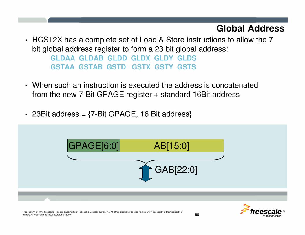
• HCS12X has a complete set of Load & Store instructions to allow the 7 bit global address register to form a 23 bit global address:
GLDAA GLDAB GLDD GLDX GLDY GLDS
GSTAA GSTAB GSTD GSTX GSTY GSTS
• When such an instruction is executed the address is concatenatedfrom the new 7-Bit GPAGE register + standard 16Bit address
• 23Bit address = {7-Bit GPAGE, 16 Bit address}
Global Address
GPAGE[6:0] AB[15:0]
GAB[22:0]
TMFreescale™ and the Freescale logo are trademarks of Freescale Semiconductor, Inc. All other product or service names are the property of their respective owners. © Freescale Semiconductor, Inc. 2006. 61
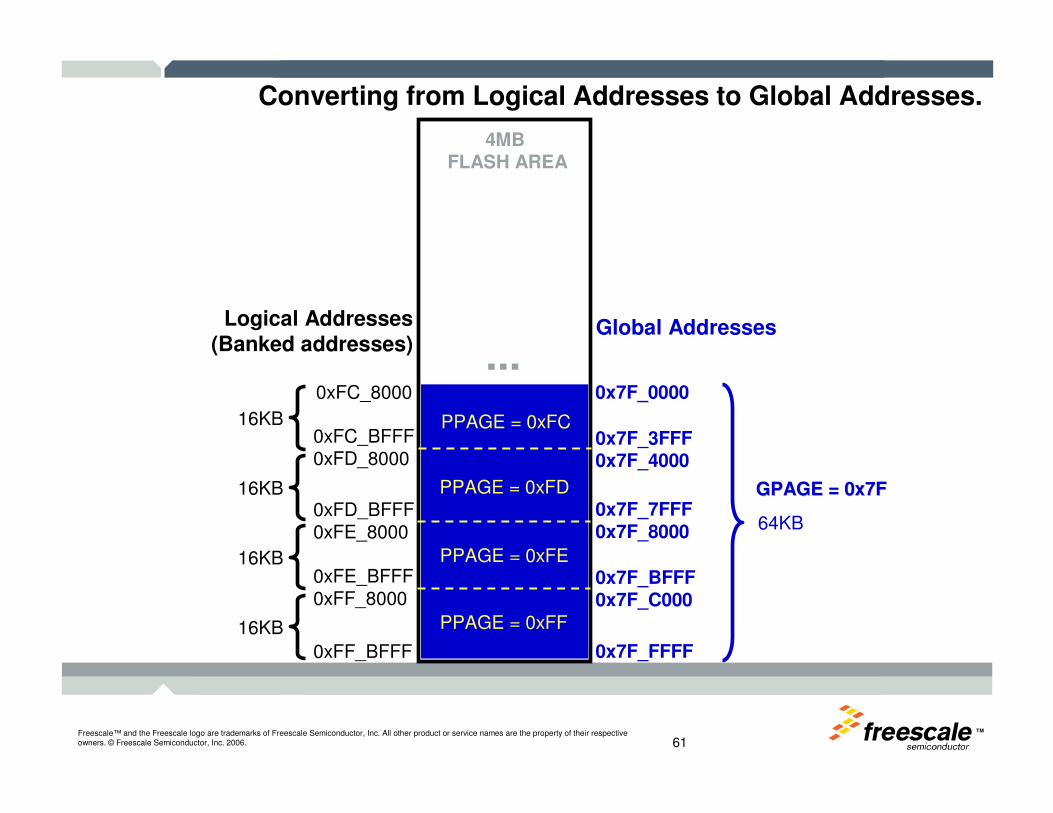
Converting from Logical Addresses to Global Addresses.
4MB FLASH AREA
PPAGE = 0xFE
PPAGE = 0xFF
0xFC_BFFF0xFD_8000
0xFE_BFFF0xFF_8000
0x7F_FFFF
0xFD_BFFF0xFE_8000
...
0x7F_BFFF0x7F_C000
0x7F_7FFF0x7F_8000
0x7F_3FFF0x7F_4000
PPAGE = 0xFD
Logical Addresses(Banked addresses)
Global Addresses
PPAGE = 0xFC
0xFF_BFFF
0xFC_8000 0x7F_0000
GPAGE = 0x7FGPAGE = 0x7F
64KB
16KB
16KB
16KB
16KB
TM
Freescale™ and the Freescale logo are trademarks of Freescale Semiconductor, Inc. All other product or service names are the property of their respective owners. © Freescale Semiconductor, Inc. 2006.
XGATE Briefing
TMFreescale™ and the Freescale logo are trademarks of Freescale Semiconductor, Inc. All other product or service names are the property of their respective owners. © Freescale Semiconductor, Inc. 2006. 63
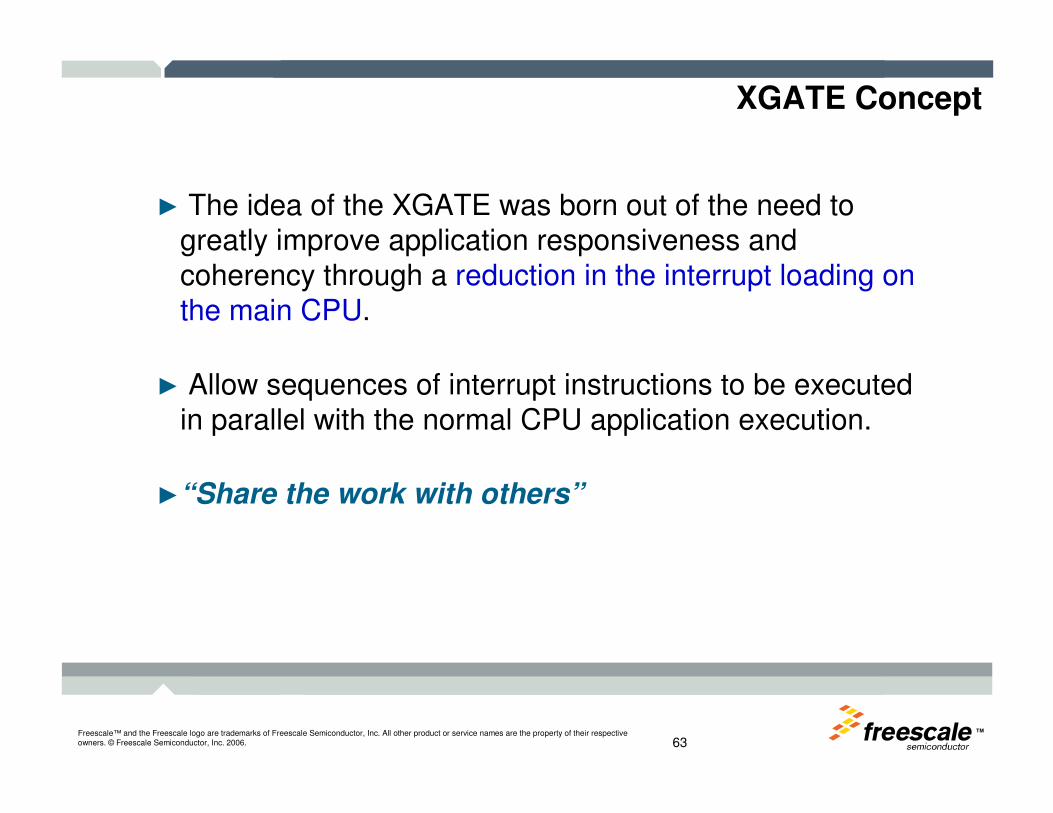
XGATE Concept
► The idea of the XGATE was born out of the need to greatly improve application responsiveness and coherency through a reduction in the interrupt loading on the main CPU.
► Allow sequences of interrupt instructions to be executed in parallel with the normal CPU application execution.
►“Share the work with others”

TMFreescale™ and the Freescale logo are trademarks of Freescale Semiconductor, Inc. All other product or service names are the property of their respective owners. © Freescale Semiconductor, Inc. 2006. 64
XGATE Concept
CPU Running application code
CPU Running application code
S12
S12X
Interrupt request
CPU Stalls
Application code
to service IRQ
Interrupt complete
CPU Running application code
XGATE stopped
CPU Running application code
XGATE completely handles the IRQ
CPU Running application code
XGATE stopped
TMFreescale™ and the Freescale logo are trademarks of Freescale Semiconductor, Inc. All other product or service names are the property of their respective owners. © Freescale Semiconductor, Inc. 2006. 65
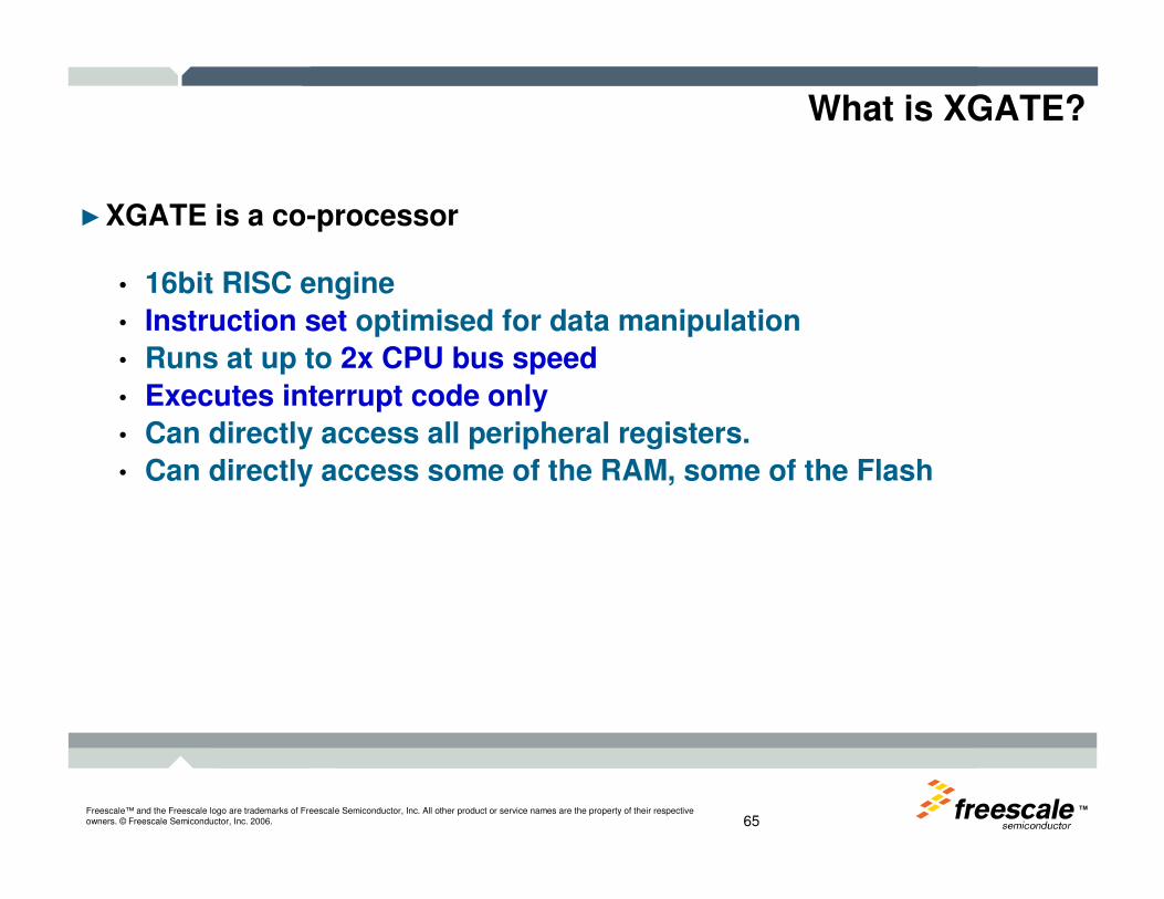
What is XGATE?
►XGATE is a co-processor
• 16bit RISC engine
• Instruction set optimised for data manipulation
• Runs at up to 2x CPU bus speed
• Executes interrupt code only
• Can directly access all peripheral registers.
• Can directly access some of the RAM, some of the Flash

TMFreescale™ and the Freescale logo are trademarks of Freescale Semiconductor, Inc. All other product or service names are the property of their respective owners. © Freescale Semiconductor, Inc. 2006. 66
What is XGATE?
►XGATE is Interrupt driven
• Code executed by XGATE has to be inside an interrupt routine.
• Cannot execute code that is not associated with an interrupt.
• Most of the interrupts can be routed to the XGATE.
• XGATE can also trigger a CPU interrupt when finished.
• When not executing code, XGATE is idle.
TMFreescale™ and the Freescale logo are trademarks of Freescale Semiconductor, Inc. All other product or service names are the property of their respective owners. © Freescale Semiconductor, Inc. 2006. 67
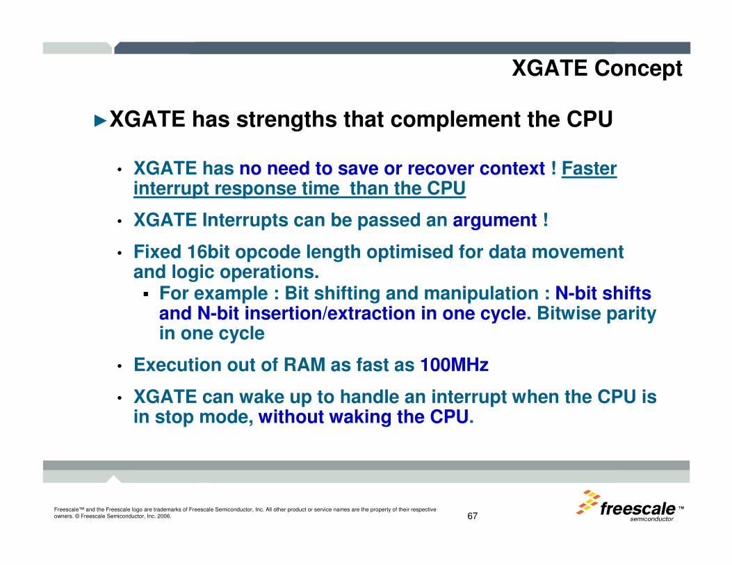
XGATE Concept
►XGATE has strengths that complement the CPU
• XGATE has no need to save or recover context ! Faster interrupt response time than the CPU
• XGATE Interrupts can be passed an argument !
• Fixed 16bit opcode length optimised for data movement and logic operations. � For example : Bit shifting and manipulation : N-bit shifts
and N-bit insertion/extraction in one cycle. Bitwise parity in one cycle
• Execution out of RAM as fast as 100MHz
• XGATE can wake up to handle an interrupt when the CPU is in stop mode, without waking the CPU.

TMFreescale™ and the Freescale logo are trademarks of Freescale Semiconductor, Inc. All other product or service names are the property of their respective owners. © Freescale Semiconductor, Inc. 2006. 68
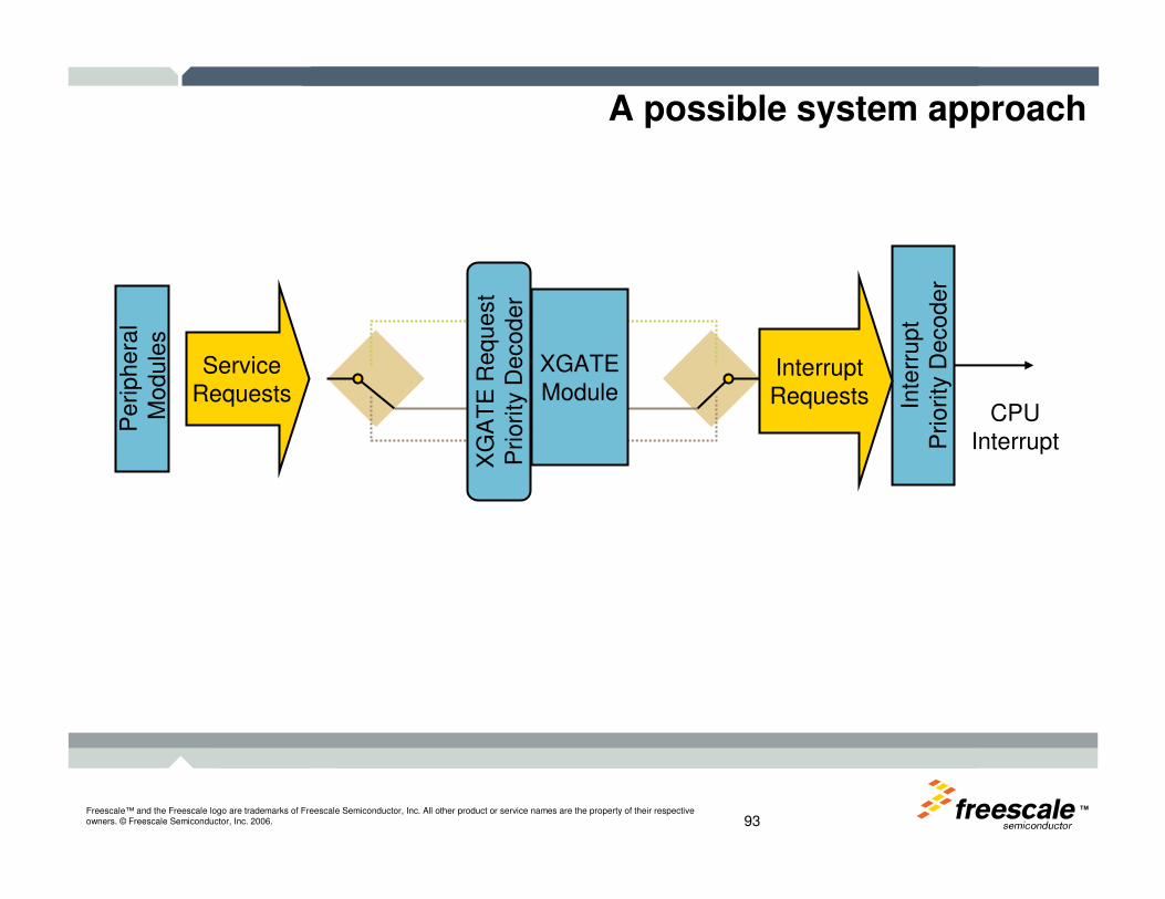
A possible system approachP
eriphera
lM
odule
s
Inte
rrup
tP
riority
Decoder
CPUInterrupt
XGATEModule
XG
AT
E R
equest
Priority
Decoder
ServiceRequests
InterruptRequests
TM
Freescale™ and the Freescale logo are trademarks of Freescale Semiconductor, Inc. All other product or service names are the property of their respective owners. © Freescale Semiconductor, Inc. 2006.
XGATE Programming Model and Instruction Set
TMFreescale™ and the Freescale logo are trademarks of Freescale Semiconductor, Inc. All other product or service names are the property of their respective owners. © Freescale Semiconductor, Inc. 2006. 70
R1R1
CCR (N,V,C,Z)CCR (N,V,C,Z) 001515
PCPC 001515
R7R7 001515
R6R6 001515
R5R5 001515
R4R4 001515
R3R3 001515
R2R2 001515
001515
R0R0 001515
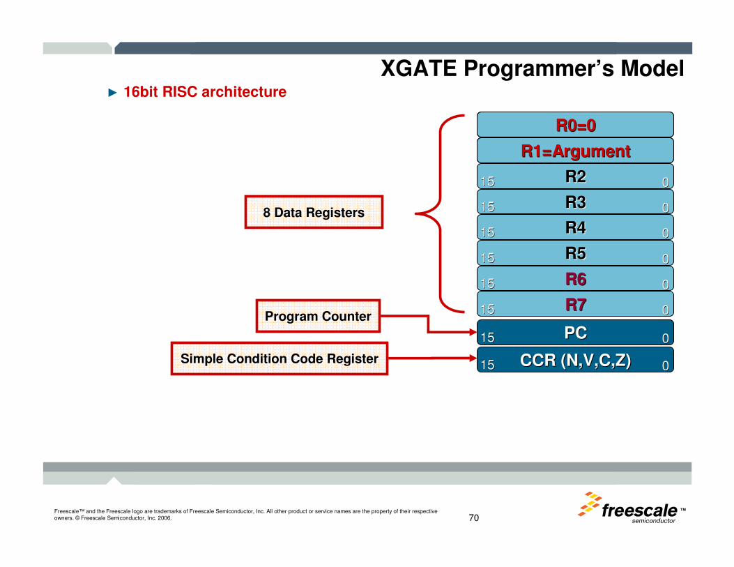
XGATE Programmer’s Model► 16bit RISC architecture
R1=ArgumentR1=Argument
R0=0R0=0
8 Data Registers
Program Counter
Simple Condition Code Register

TMFreescale™ and the Freescale logo are trademarks of Freescale Semiconductor, Inc. All other product or service names are the property of their respective owners. © Freescale Semiconductor, Inc. 2006. 71
Register usage by the module and by the compiler
CCR (N,V,C,Z)CCR (N,V,C,Z) 001515
PCPC 001515
R7R7-- Stack PointerStack Pointer 001515
R6R6--Function CallsFunction Calls 001515
R5R5 001515
R4R4 001515
R3R3 001515
R2R2 001515
R1R1 001515
R0R0 001515
Reading R0 results in value ZERO. Writing to R0 discards the result. (but modifies CCR)
Xgate module initializes R1 with value of an user-selected
argument (Useful for code reuse!)
C-compiler uses R6 as a base for function calls
C-compiler uses R7 as a stack pointer
General purpose
R0=0R0=0
R1=ArgumentR1=Argument

TMFreescale™ and the Freescale logo are trademarks of Freescale Semiconductor, Inc. All other product or service names are the property of their respective owners. © Freescale Semiconductor, Inc. 2006. 72
XGATE Instruction Set
► Strict Load/Store Architecture
• All instructions (except for inherent instructions) involve at least one of the registers R0-R7
• Must work with word-aligned accesses!
► The instruction set is optimised for fast data handling and response to events
• Bit shift or rotate in one cycle
• Word addition/subtraction in one cycle
• 16 bit parity calculation in one cycle
• Store word to memory in two cycles
• Set/Clear semaphore in two cycles
• Bit stuffing and extraction in one cycle
• No multiply or divide instructions
CCR (N,V,C,Z)CCR (N,V,C,Z) 001515
PCPC 001515
R6R6 001515
R6R6 001515
R5R5 001515
R4R4 001515
R3R3 001515
R2R2 001515
R1 = BaseR1 = Base 001515
R0=0R0=0 001515
TMFreescale™ and the Freescale logo are trademarks of Freescale Semiconductor, Inc. All other product or service names are the property of their respective owners. © Freescale Semiconductor, Inc. 2006. 73
XGATE Concept
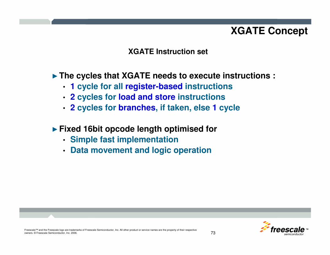
►The cycles that XGATE needs to execute instructions :
• 1 cycle for all register-based instructions
• 2 cycles for load and store instructions
• 2 cycles for branches, if taken, else 1 cycle
►Fixed 16bit opcode length optimised for
• Simple fast implementation
• Data movement and logic operation
XGATE Instruction set
TMFreescale™ and the Freescale logo are trademarks of Freescale Semiconductor, Inc. All other product or service names are the property of their respective owners. © Freescale Semiconductor, Inc. 2006. 74
XGATE Concept
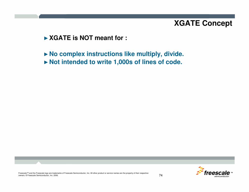
►XGATE is NOT meant for :
►No complex instructions like multiply, divide.
►Not intended to write 1,000s of lines of code.
TMFreescale™ and the Freescale logo are trademarks of Freescale Semiconductor, Inc. All other product or service names are the property of their respective owners. © Freescale Semiconductor, Inc. 2006. 75
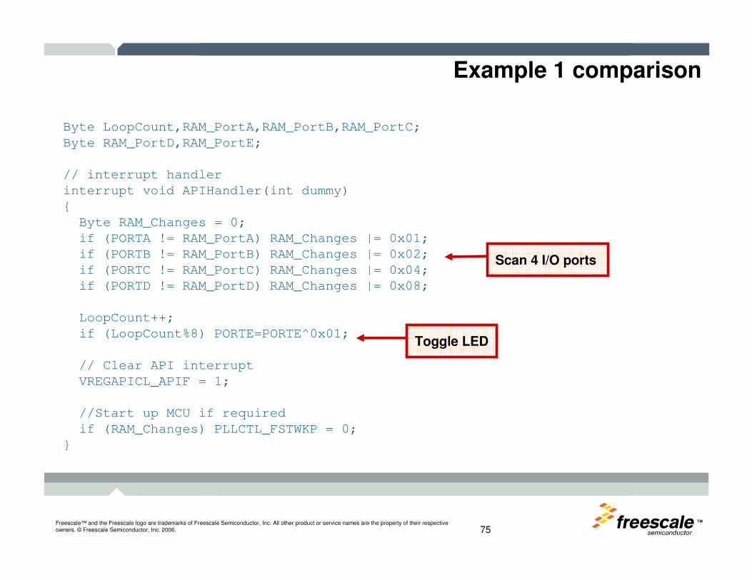
Example 1 comparison
Byte LoopCount,RAM_PortA,RAM_PortB,RAM_PortC;
Byte RAM_PortD,RAM_PortE;
// interrupt handler
interrupt void APIHandler(int dummy)
{
Byte RAM_Changes = 0;
if (PORTA != RAM_PortA) RAM_Changes |= 0x01;
if (PORTB != RAM_PortB) RAM_Changes |= 0x02;
if (PORTC != RAM_PortC) RAM_Changes |= 0x04;
if (PORTD != RAM_PortD) RAM_Changes |= 0x08;
LoopCount++;
if (LoopCount%8) PORTE=PORTE^0x01;
// Clear API interrupt
VREGAPICL_APIF = 1;
//Start up MCU if required
if (RAM_Changes) PLLCTL_FSTWKP = 0;
}
Toggle LED
Scan 4 I/O ports

TMFreescale™ and the Freescale logo are trademarks of Freescale Semiconductor, Inc. All other product or service names are the property of their respective owners. © Freescale Semiconductor, Inc. 2006. 76
71
103
92
102
0
20
40
60
80
100
120
Code size Cycle count
XGate
CPU
Example 1 comparison results
Code size and cycle count
Source: Code compiled with CodeWarrior 4.1, results from simulator
XGATE completes in 90% of CPU time
TMFreescale™ and the Freescale logo are trademarks of Freescale Semiconductor, Inc. All other product or service names are the property of their respective owners. © Freescale Semiconductor, Inc. 2006. 77
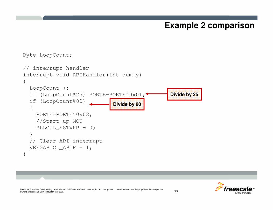
Example 2 comparison
Byte LoopCount;
// interrupt handler
interrupt void APIHandler(int dummy)
{
LoopCount++;
if (LoopCount%25) PORTE=PORTE^0x01;
if (LoopCount%80)
{
PORTE=PORTE^0x02;
//Start up MCU
PLLCTL_FSTWKP = 0;
}
// Clear API interrupt
VREGAPICL_APIF = 1;
}
Divide by 80
Divide by 25
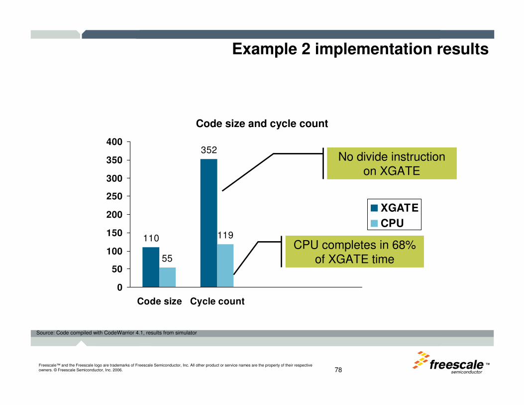
TMFreescale™ and the Freescale logo are trademarks of Freescale Semiconductor, Inc. All other product or service names are the property of their respective owners. © Freescale Semiconductor, Inc. 2006. 78
55
119
352
110
0
50
100
150
200
250
300
350
400
Code size Cycle count
XGATE
CPU
Example 2 implementation results
Code size and cycle count
Source: Code compiled with CodeWarrior 4.1, results from simulator
CPU completes in 68% of XGATE time
No divide instruction on XGATE
TMFreescale™ and the Freescale logo are trademarks of Freescale Semiconductor, Inc. All other product or service names are the property of their respective owners. © Freescale Semiconductor, Inc. 2006. 79
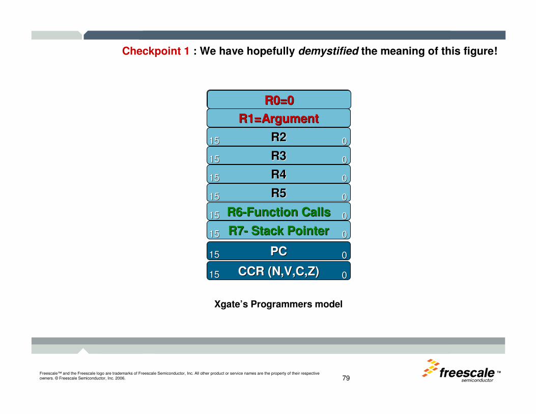
Checkpoint 1 : We have hopefully demystified the meaning of this figure!
CCR (N,V,C,Z)CCR (N,V,C,Z) 001515
PCPC 001515
R7R7-- Stack PointerStack Pointer 001515
R6R6--Function CallsFunction Calls 001515
R5R5 001515
R4R4 001515
R3R3 001515
R2R2 001515
R1R1 001515
R0R0 001515 R0=0R0=0
R1=ArgumentR1=Argument
Xgate’s Programmers model
TM
Freescale™ and the Freescale logo are trademarks of Freescale Semiconductor, Inc. All other product or service names are the property of their respective owners. © Freescale Semiconductor, Inc. 2006.
The XGATE’s Memory map
TMFreescale™ and the Freescale logo are trademarks of Freescale Semiconductor, Inc. All other product or service names are the property of their respective owners. © Freescale Semiconductor, Inc. 2006. 81
XGate memory map
►The XGate can address 64k of memory
2k of peripheral register space30k of FLASHUp to 32k of RAM(Consult your device’s datasheet)
► XGate and CPU share access to the same physical memory• This allows both processors to communicate and share tasks
► The S12X hardware automatically manages memory access• The MCU provides an access protection system (e.g., MPU in
S12XEP100) to prevent the CPU or XGate disturbing each other’s RAM contents
• Memory can be divided into shared, XGate write only and CPU write only regions� The size of each region is configurable
64k
2k Registers
32kRAM
Flash30k
TMFreescale™ and the Freescale logo are trademarks of Freescale Semiconductor, Inc. All other product or service names are the property of their respective owners. © Freescale Semiconductor, Inc. 2006. 82
XGate Memory Space
0x00_0000
0x00_07FF
0x0F_8000
0x0F_FFFF
0x78_0800
0x78_7FFF64k
2k Registers
32k RAM
30k Flash
$8000
$FFFF
$0000
$07FF$0800
$7FFF64kByte
XGate Space
CorrespondingGlobal Addresses
PAGE_E0
PAGE_E1
RAM PAGE_F8
RAM PAGE_F9
RAM PAGE_FA
RAM PAGE_FB
RAM PAGE_FC
RAM PAGE_FD
RAM PAGE_FE
RAM PAGE_FF
XGATE ADDRESSES
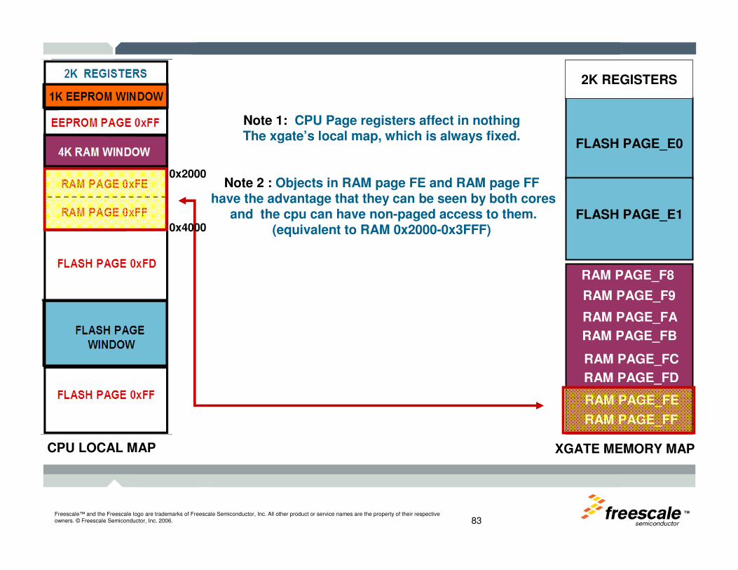
TMFreescale™ and the Freescale logo are trademarks of Freescale Semiconductor, Inc. All other product or service names are the property of their respective owners. © Freescale Semiconductor, Inc. 2006. 83
FLASH PAGE_E0
FLASH PAGE_E1
RAM PAGE_F8
RAM PAGE_F9
RAM PAGE_FA
RAM PAGE_FB
RAM PAGE_FC
RAM PAGE_FD
RAM PAGE_FE
RAM PAGE_FF
2K REGISTERS
XGATE MEMORY MAPCPU LOCAL MAP
Note 1: CPU Page registers affect in nothing The xgate’s local map, which is always fixed.
Note 2 : Objects in RAM page FE and RAM page FF have the advantage that they can be seen by both cores
and the cpu can have non-paged access to them.(equivalent to RAM 0x2000-0x3FFF)
0x2000
0x4000

TMFreescale™ and the Freescale logo are trademarks of Freescale Semiconductor, Inc. All other product or service names are the property of their respective owners. © Freescale Semiconductor, Inc. 2006. 84
Converting from Global addresses to Xgate addresses
$8000
$FFFF
$0000
$07FF$0800
0x00_0000
0x00_07FF
0x0F_8000
0x0F_FFFF
0x78_0800
0x78_7FFF64k
2k Registers
32k RAM
30k Flash
$7FFF64kByte
XGate Space
CorrespondingGlobal Addresses
PAGE_E0
PAGE_E1
RAM PAGE_F8
RAM PAGE_F9
RAM PAGE_FA
RAM PAGE_FB
RAM PAGE_FC
RAM PAGE_FD
RAM PAGE_FE
RAM PAGE_FF
XGATE ADDRESSES
TMFreescale™ and the Freescale logo are trademarks of Freescale Semiconductor, Inc. All other product or service names are the property of their respective owners. © Freescale Semiconductor, Inc. 2006. 85
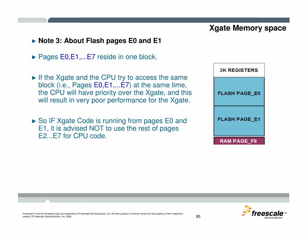
Xgate Memory space
► Note 3: About Flash pages E0 and E1
► Pages E0,E1,...E7 reside in one block.
► If the Xgate and the CPU try to access the same block (i.e., Pages E0,E1,...E7) at the same time, the CPU will have priority over the Xgate, and this will result in very poor performance for the Xgate.
► So IF Xgate Code is running from pages E0 and E1, it is advised NOT to use the rest of pages E2...E7 for CPU code.
TM
Freescale™ and the Freescale logo are trademarks of Freescale Semiconductor, Inc. All other product or service names are the property of their respective owners. © Freescale Semiconductor, Inc. 2006.
XGATE Thread and Cronfiguation
TMFreescale™ and the Freescale logo are trademarks of Freescale Semiconductor, Inc. All other product or service names are the property of their respective owners. © Freescale Semiconductor, Inc. 2006. 87
The Interrupt Controller Module (XINT)
► The individual event which trigger execution of XGATE code are provided by the interrupt controller. Let’s take some minutes to see
how this interrupt controller functions.

TMFreescale™ and the Freescale logo are trademarks of Freescale Semiconductor, Inc. All other product or service names are the property of their respective owners. © Freescale Semiconductor, Inc. 2006. 88
The Interrupt Controller Module (XINT)
► In brief, the XINT module is responsible for :
• Directing interrupts to be handled by either the XGATE or the CPU. (User configurable)
• Determining which of the pending CPU interrupts has the highest priority. 7 user-defined levels of priority are accepted by the CPU.
• Determining which of the pending XGATE interrupts has the highest priority. 2 user-defined levels of priority are accepted by the XGATE.
• Determining the location of CPU vector table. CPU interrupt vectors can be placed in any 256 byte page. ( Reset vectors cannot be moved.)
Remarks :
• Xgate Vector table can be placed in any Xgate accessible memory area.
• An Interrupt running on XGATE can now be interrupted!(For XGATE Version 3 only)
TMFreescale™ and the Freescale logo are trademarks of Freescale Semiconductor, Inc. All other product or service names are the property of their respective owners. © Freescale Semiconductor, Inc. 2006. 89
The Interrupt Controller Module (XINT)
CPU Interrupt vectors can be relocated: By writing a value to a specific register(XGVBR), the Vector Base is changed. Vector Base defaults to 0xFF.
Reset vectors cannot be relocated.
A number, called Channel ID is used by the XGATE when an interrupt is redirected to it. Each interrupt source that can be handled by XGATE has a channel ID associated.
In S12XEP100 device, possible channel IDs are 0x1E to 0x78 = 91 interrupt sources can be redirected to XGATE.
Out of reset, XINT configures all interrupts to level 1 and directs them to the CPU.
Interrupt VectorsInterrupt Vectors

TMFreescale™ and the Freescale logo are trademarks of Freescale Semiconductor, Inc. All other product or service names are the property of their respective owners. © Freescale Semiconductor, Inc. 2006. 90
The Interrupt Controller Module (XINT)

TMFreescale™ and the Freescale logo are trademarks of Freescale Semiconductor, Inc. All other product or service names are the property of their respective owners. © Freescale Semiconductor, Inc. 2006. 91
The Interrupt Controller Module (XINT)
TMFreescale™ and the Freescale logo are trademarks of Freescale Semiconductor, Inc. All other product or service names are the property of their respective owners. © Freescale Semiconductor, Inc. 2006. 92
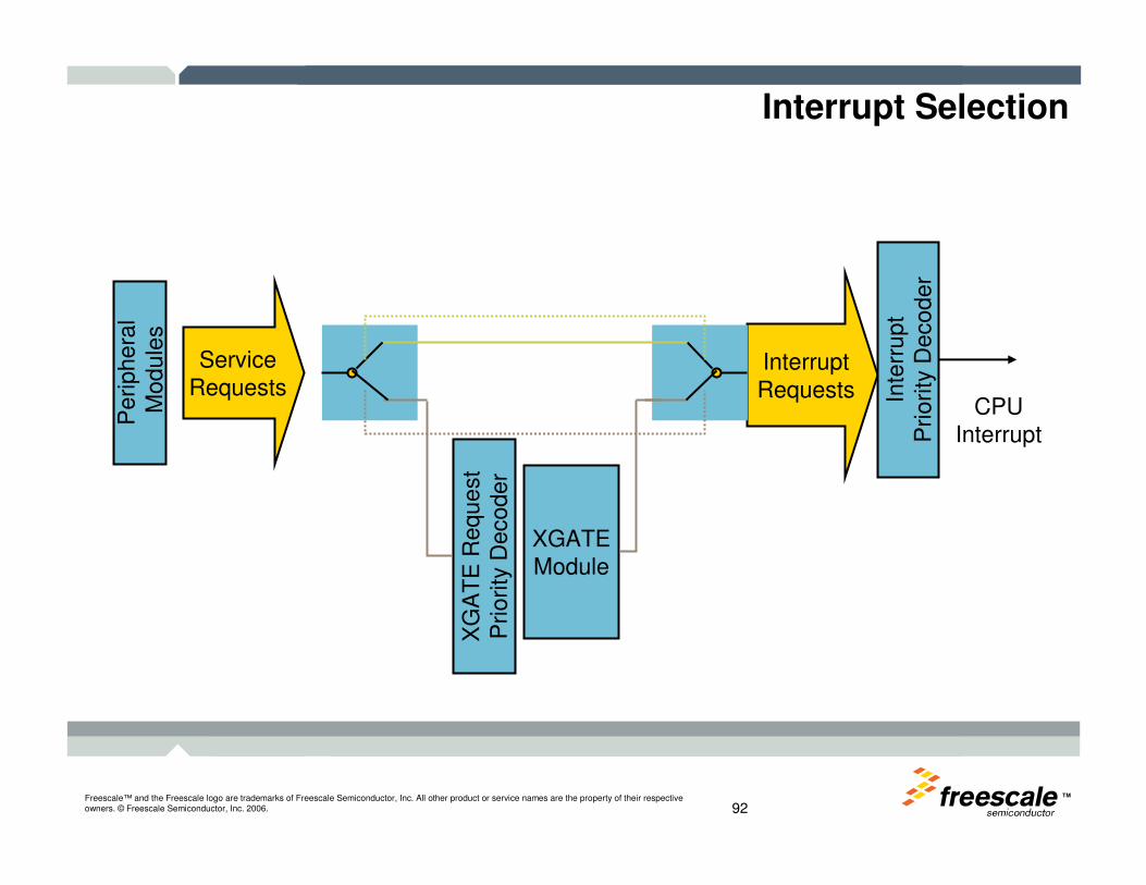
Interrupt SelectionP
eriphera
lM
odule
s
ServiceRequests
InterruptRequests In
terr
up
tP
riority
Decoder
XGATEModule
XG
AT
E R
equest
Priority
Decoder
CPUInterrupt
TMFreescale™ and the Freescale logo are trademarks of Freescale Semiconductor, Inc. All other product or service names are the property of their respective owners. © Freescale Semiconductor, Inc. 2006. 93
A possible system approachP
eriphera
lM
odule
s
Inte
rrup
tP
riority
Decoder
CPUInterrupt
XGATEModule
XG
AT
E R
equest
Priority
Decoder
ServiceRequests
InterruptRequests

TMFreescale™ and the Freescale logo are trademarks of Freescale Semiconductor, Inc. All other product or service names are the property of their respective owners. © Freescale Semiconductor, Inc. 2006. 94
The Interrupt Controller Module (XINT)
► How to route an interrupt to the XGATE ?
► Interrupt Request Configuration Data Register: INTCF_DATA
When set to 1, this bit will make
the XGATE handle the associated interrupt.These 3 bits contain the priority level
from 0 to 7. If priority = 0, interrupt is disabled.
Example : Writing a value of 0x81 to this register will direct the corresponding interrupt to the Xgate with a priority of 1.

TMFreescale™ and the Freescale logo are trademarks of Freescale Semiconductor, Inc. All other product or service names are the property of their respective owners. © Freescale Semiconductor, Inc. 2006. 95
Configuring the Interrupt module
► 91 interrupt sources = 91 registers!
► To save space in the memory map, these configuration registers are grouped in packs of eight. All of these “pages” of 8 registers overlap each other. To access the appropriate page, you first need to write to a page select register.
Interrupt configuration register
Choose interrupt configuration by selecting appropriate page of registers
RQST| | | | |ILVL
RQST| | | | |ILVL
RQST| | | | |ILVL
RQST| | | | |ILVL
RQST| | | | |ILVL
RQST| | | | |ILVL
RQST| | | | |ILVL
RQST| | | | |ILVL

TMFreescale™ and the Freescale logo are trademarks of Freescale Semiconductor, Inc. All other product or service names are the property of their respective owners. © Freescale Semiconductor, Inc. 2006. 96
1. Configuring interrupts
► How to write to the appropiate “Interrupt Request Configuration Data Register”?
► Interrupt configuration address register: INT_CFADDR
Writing the lower byte of the interrupt address into this register will show the appropiate page of configuration registers into the map.
TMFreescale™ and the Freescale logo are trademarks of Freescale Semiconductor, Inc. All other product or service names are the property of their respective owners. © Freescale Semiconductor, Inc. 2006. 97
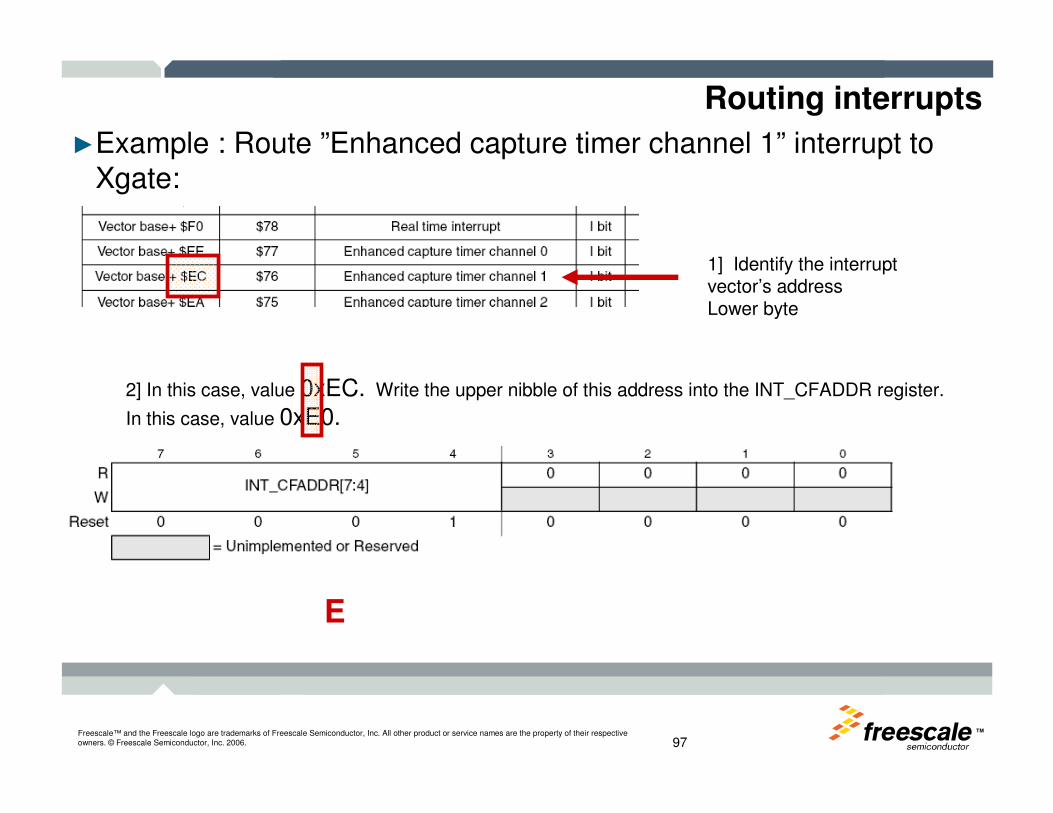
Routing interrupts
►Example : Route ”Enhanced capture timer channel 1” interrupt to Xgate:
1] Identify the interrupt vector’s addressLower byte
2] In this case, value 0xEC. Write the upper nibble of this address into the INT_CFADDR register.
In this case, value 0xE0.
E

TMFreescale™ and the Freescale logo are trademarks of Freescale Semiconductor, Inc. All other product or service names are the property of their respective owners. © Freescale Semiconductor, Inc. 2006. 98
Routing Interrupts
RQST| | | | |ILVL
RQST| | | | |ILVL
RQST| | | | |ILVL
RQST| | | | |ILVL
RQST| | | | |ILVL
RQST| | | | |ILVL
RQST| | | | |ILVL
RQST| | | | |ILVL
INT_CFADDR=0xE0
Page of configuration registers starting with Address E is shown
3] To write to appropiate register inside this page do:
Register number = C / 2 = 6.
4] Write to the sixth register inside this page(count starts with zero)
INT_CFDATA6 = 0x81
E 0E 2E 4E 6E 8E AE CE E
Routing vector at address “Vector base + 0xEC”
0.1.2.3.4.5.6.7.
TMFreescale™ and the Freescale logo are trademarks of Freescale Semiconductor, Inc. All other product or service names are the property of their respective owners. © Freescale Semiconductor, Inc. 2006. 99
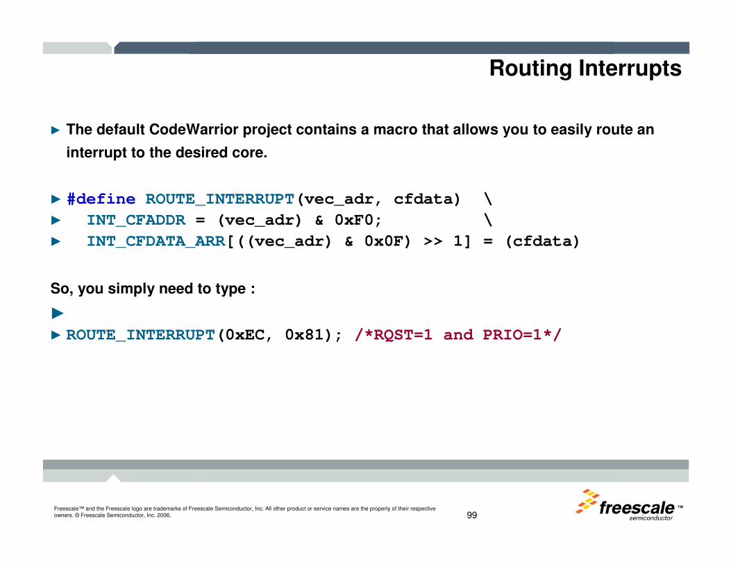
► The default CodeWarrior project contains a macro that allows you to easily route an
interrupt to the desired core.
► #define ROUTE_INTERRUPT(vec_adr, cfdata) \
► INT_CFADDR = (vec_adr) & 0xF0; \
► INT_CFDATA_ARR[((vec_adr) & 0x0F) >> 1] = (cfdata)
►
► ROUTE_INTERRUPT(0xEC, 0x81); /*RQST=1 and PRIO=1*/
Routing Interrupts
So, you simply need to type :

TMFreescale™ and the Freescale logo are trademarks of Freescale Semiconductor, Inc. All other product or service names are the property of their respective owners. © Freescale Semiconductor, Inc. 2006. 100
2. Initializing Xgate Vector table
► How to initialize the Xgate’s vector table?
► 1] By writing to the Xgate Vector Base register (XGVBR).
► Xgate expects to have a vector table somewhere in memory where the addresses of each interrupt service routine are listed, starting with channel 0.
Address of Channel 0 interruptAddress of Channel 1 interruptAddress of Channel 2 interruptAddress of Channel 3 interruptAddress of Channel 4 interruptAddress of Channel 5 interrupt
( ...)
Address of last implemented Xgate Channel
XGVBR should point to this
start address.

TMFreescale™ and the Freescale logo are trademarks of Freescale Semiconductor, Inc. All other product or service names are the property of their respective owners. © Freescale Semiconductor, Inc. 2006. 101
Initializing Xgate Vector table
Address of Channel 0 interruptAddress of Channel 1 interruptAddress of Channel 2 interruptAddress of Channel 3 interruptAddress of Channel 4 interruptAddress of Channel 5 interrupt
( ...)
Address of last implemented Xgate Channel
XGVBR should point to this
start address.
Typically, not all Xgate channels are implemented. They are there for future use.
For example, In the XEP100 the first implemented Xgate channel is Channel 0x1E (ATD1).
TMFreescale™ and the Freescale logo are trademarks of Freescale Semiconductor, Inc. All other product or service names are the property of their respective owners. © Freescale Semiconductor, Inc. 2006. 102
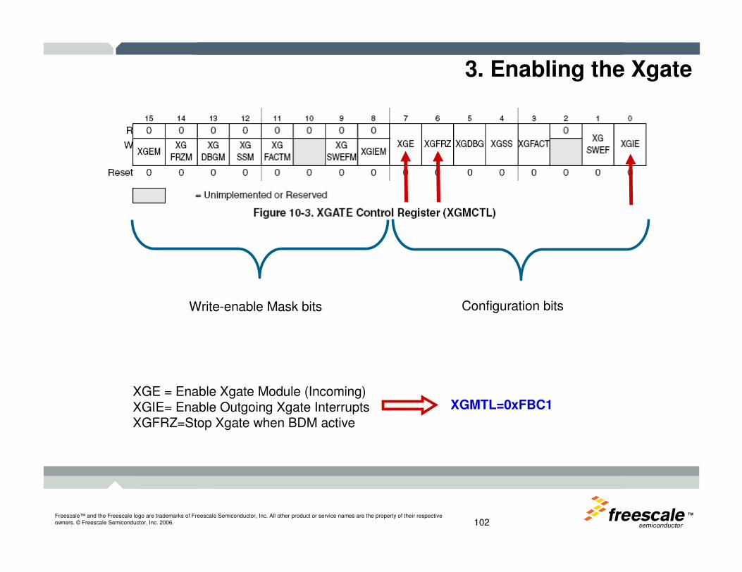
3. Enabling the Xgate
Write-enable Mask bits Configuration bits
XGMTL=0xFBC1XGE = Enable Xgate Module (Incoming)XGIE= Enable Outgoing Xgate InterruptsXGFRZ=Stop Xgate when BDM active
TM
Freescale™ and the Freescale logo are trademarks of Freescale Semiconductor, Inc. All other product or service names are the property of their respective owners. © Freescale Semiconductor, Inc. 2006.
XGATE Software Trigger & Semaphore
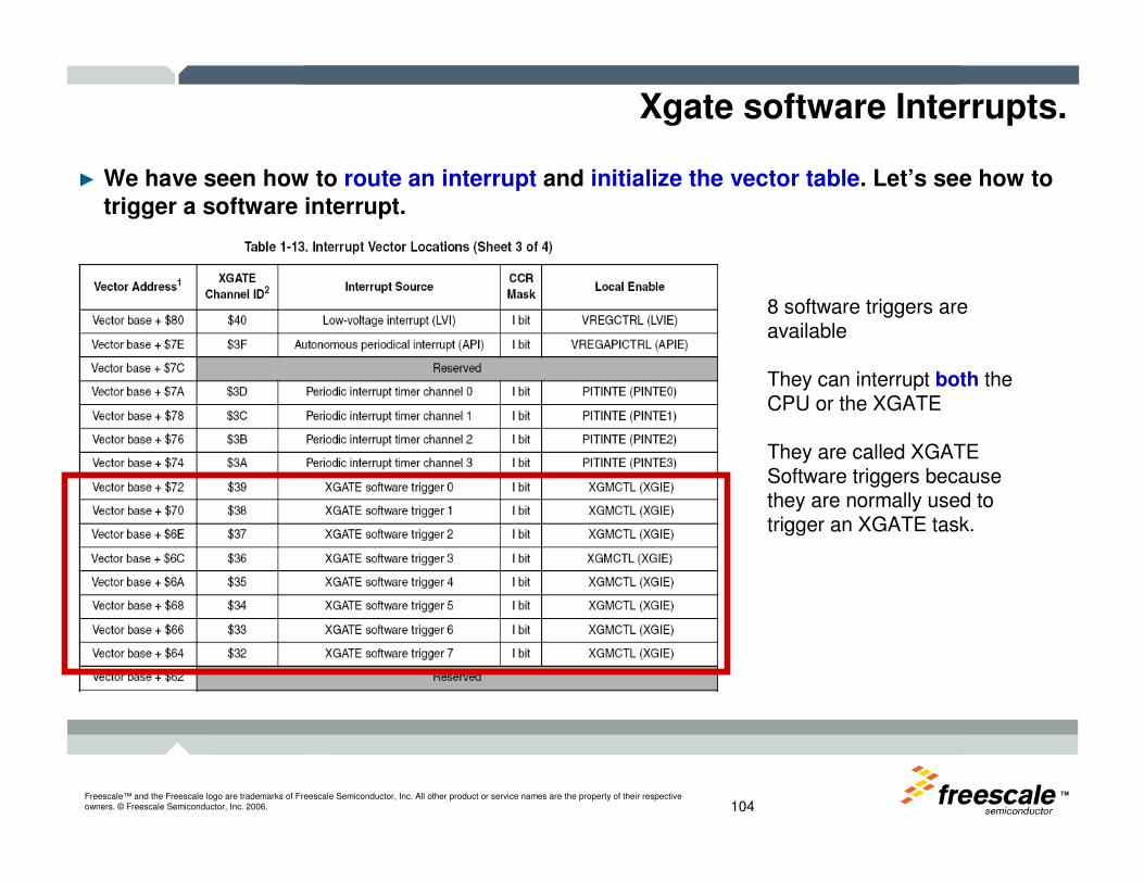
TMFreescale™ and the Freescale logo are trademarks of Freescale Semiconductor, Inc. All other product or service names are the property of their respective owners. © Freescale Semiconductor, Inc. 2006. 104
Xgate software Interrupts.
► We have seen how to route an interrupt and initialize the vector table. Let’s see how to trigger a software interrupt.
8 software triggers are available
They can interrupt both the CPU or the XGATE
They are called XGATE Software triggers because they are normally used to trigger an XGATE task.
TMFreescale™ and the Freescale logo are trademarks of Freescale Semiconductor, Inc. All other product or service names are the property of their respective owners. © Freescale Semiconductor, Inc. 2006. 105
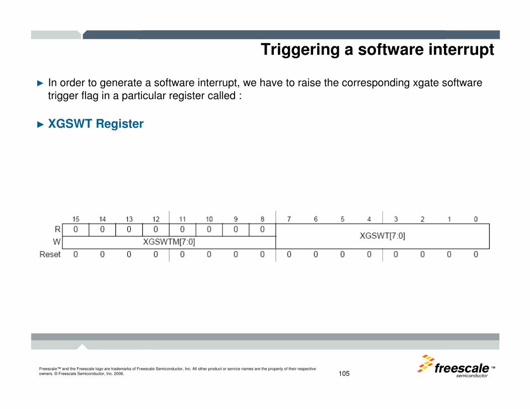
Triggering a software interrupt
► In order to generate a software interrupt, we have to raise the corresponding xgate software trigger flag in a particular register called :
► XGSWT Register
TMFreescale™ and the Freescale logo are trademarks of Freescale Semiconductor, Inc. All other product or service names are the property of their respective owners. © Freescale Semiconductor, Inc. 2006. 106
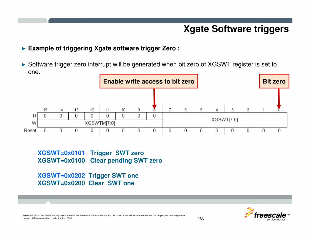
Xgate Software triggers
► Example of triggering Xgate software trigger Zero :
► Software trigger zero interrupt will be generated when bit zero of XGSWT register is set to one.
Bit zeroEnable write access to bit zero
XGSWT=0x0101 Trigger SWT zeroXGSWT=0x0100 Clear pending SWT zero
XGSWT=0x0202 Trigger SWT oneXGSWT=0x0200 Clear SWT one
TMFreescale™ and the Freescale logo are trademarks of Freescale Semiconductor, Inc. All other product or service names are the property of their respective owners. © Freescale Semiconductor, Inc. 2006. 107
Xgate Software triggers
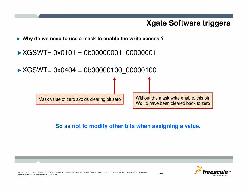
► Why do we need to use a mask to enable the write access ?
►XGSWT= 0x0101 = 0b00000001_00000001
►XGSWT= 0x0404 = 0b00000100_00000100
Mask value of zero avoids clearing bit zero Without the mask write enable, this bit Would have been cleared back to zero
So as not to modify other bits when assigning a value.

TMFreescale™ and the Freescale logo are trademarks of Freescale Semiconductor, Inc. All other product or service names are the property of their respective owners. © Freescale Semiconductor, Inc. 2006. 108
Semaphores
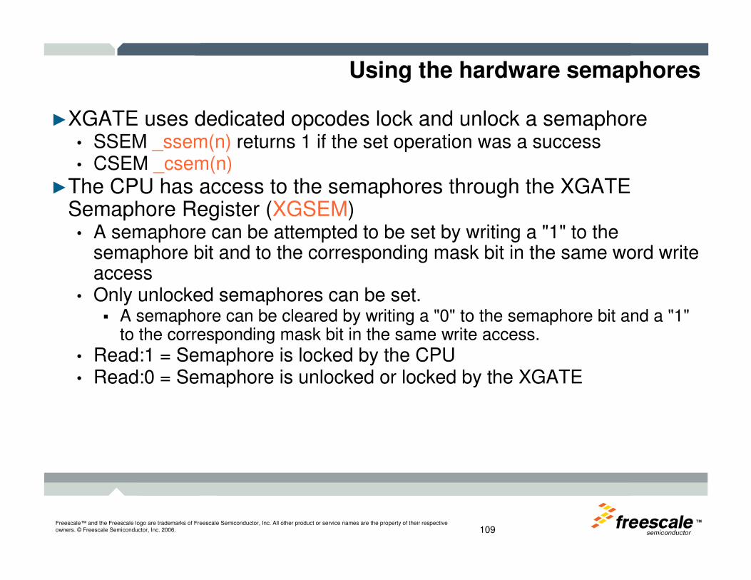
►The XGATE provides a set of eight hardware semaphores• Shared between the CPU and the XGATE
• Each semaphore can either be� Unlocked
� locked by the CPU
� locked by the XGATE
m m m m m m m m 1 0 1 1 0 0 0 1
Semaphores indicate the availability of shared resource
Semaphore masks allow atomic write access
unlocked
CPU
Writ
e
“1_1
”
XGATE
SSEM
CPU
Writ
e
“1_0
”XG
ATECSEM
Lockedby XGATE
Locked byS12X_CPU
TMFreescale™ and the Freescale logo are trademarks of Freescale Semiconductor, Inc. All other product or service names are the property of their respective owners. © Freescale Semiconductor, Inc. 2006. 109
Using the hardware semaphores
►XGATE uses dedicated opcodes lock and unlock a semaphore• SSEM _ssem(n) returns 1 if the set operation was a success• CSEM _csem(n)
►The CPU has access to the semaphores through the XGATE Semaphore Register (XGSEM)
• A semaphore can be attempted to be set by writing a "1" to the semaphore bit and to the corresponding mask bit in the same word write access
• Only unlocked semaphores can be set.� A semaphore can be cleared by writing a "0" to the semaphore bit and a "1"
to the corresponding mask bit in the same write access.
• Read:1 = Semaphore is locked by the CPU• Read:0 = Semaphore is unlocked or locked by the XGATE
TMFreescale™ and the Freescale logo are trademarks of Freescale Semiconductor, Inc. All other product or service names are the property of their respective owners. © Freescale Semiconductor, Inc. 2006. 110
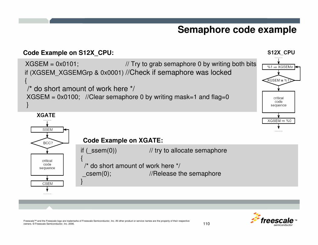
Semaphore code example
XGSEM = 0x0101; // Try to grab semaphore 0 by writing both bits
if (XGSEM_XGSEMGrp & 0x0001) //Check if semaphore was locked{
/* do short amount of work here */XGSEM = 0x0100; //Clear semaphore 0 by writing mask=1 and flag=0}
Code Example on S12X_CPU:
if (_ssem(0)) // try to allocate semaphore{/* do short amount of work here */
_csem(0); //Release the semaphore}
Code Example on XGATE:

TM
Freescale™ and the Freescale logo are trademarks of Freescale Semiconductor, Inc. All other product or service names are the property of their respective owners. © Freescale Semiconductor, Inc. 2006.
S12XS & S12P Brief
Entry Level Automotive 16-bit CAN MCU
TMFreescale™ and the Freescale logo are trademarks of Freescale Semiconductor, Inc. All other product or service names are the property of their respective owners. © Freescale Semiconductor, Inc. 2006. 112
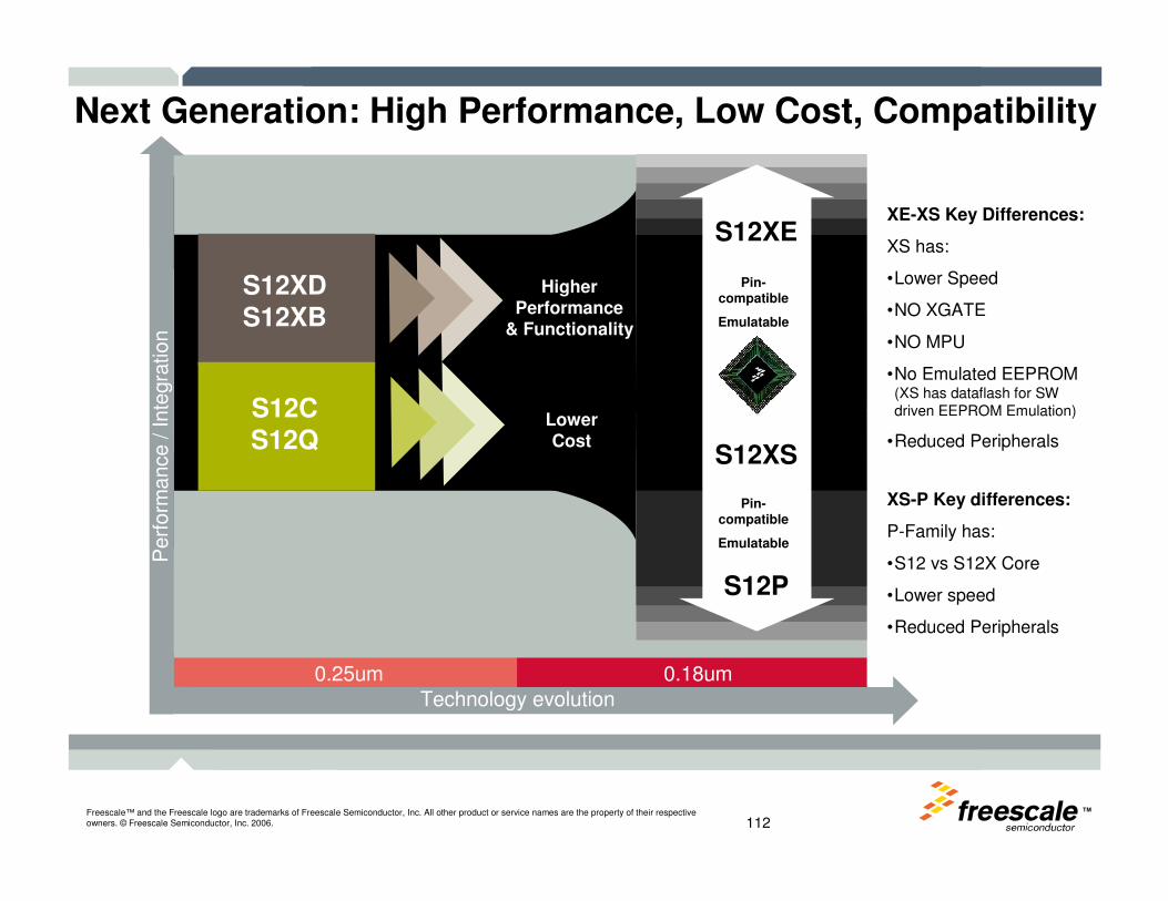
Next Generation: High Performance, Low Cost, Compatibility
XE-XS Key Differences:
XS has:
•Lower Speed
•NO XGATE
•NO MPU
•No Emulated EEPROM (XS has dataflash for SW driven EEPROM Emulation)
•Reduced Peripherals
XS-P Key differences:
P-Family has:
•S12 vs S12X Core
•Lower speed
•Reduced Peripherals
Technology evolution
S12XDS12XB
S12CS12Q
Higher Performance
& Functionality
LowerCost
Perf
orm
ance / Inte
gra
tion
0.25um 0.18um
S12XE
S12XS
S12P
Pin-compatible
Emulatable
Pin-compatible
Emulatable
TMFreescale™ and the Freescale logo are trademarks of Freescale Semiconductor, Inc. All other product or service names are the property of their respective owners. © Freescale Semiconductor, Inc. 2006. 113
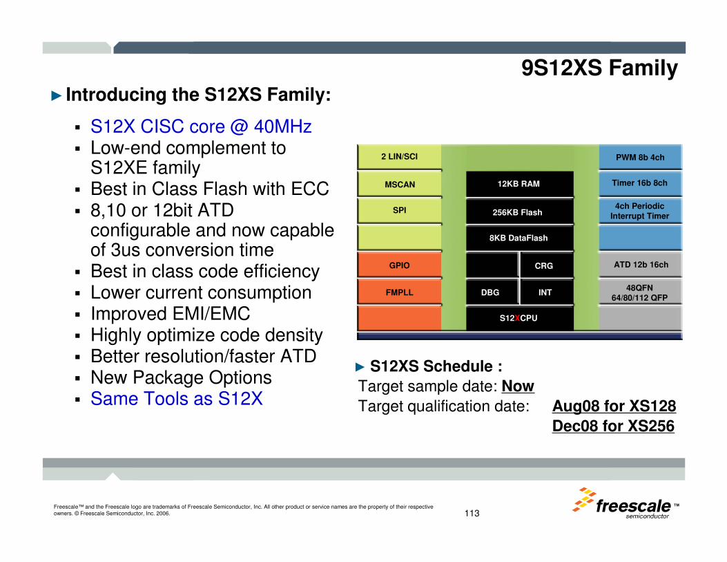
9S12XS Family► Introducing the S12XS Family:
� S12X CISC core @ 40MHz� Low-end complement to
S12XE family� Best in Class Flash with ECC� 8,10 or 12bit ATD
configurable and now capable of 3us conversion time
� Best in class code efficiency� Lower current consumption� Improved EMI/EMC� Highly optimize code density� Better resolution/faster ATD � New Package Options � Same Tools as S12X
2 LIN/SCI
SPI
GPIO
FMPLL
MSCAN
ATD 12b 16ch
Timer 16b 8ch
4ch PeriodicInterrupt Timer
PWM 8b 4ch
48QFN 64/80/112 QFP
8KB DataFlash
CRG
DBG INT
256KB Flash
12KB RAM
S12XCPU
► S12XS Schedule :
Target sample date: Now
Target qualification date: Aug08 for XS128
Dec08 for XS256
TMFreescale™ and the Freescale logo are trademarks of Freescale Semiconductor, Inc. All other product or service names are the property of their respective owners. © Freescale Semiconductor, Inc. 2006. 114
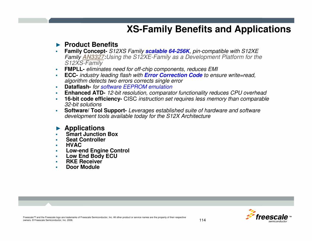
XS-Family Benefits and Applications
► Product Benefits� Family Concept- S12XS Family scalable 64-256K, pin-compatible with S12XE
Family AN3327:Using the S12XE-Family as a Development Platform for the S12XS-Family
� FMPLL- eliminates need for off-chip components, reduces EMI� ECC- industry leading flash with Error Correction Code to ensure write=read,
algorithm detects two errors corrects single error � Dataflash- for software EEPROM emulation� Enhanced ATD- 12-bit resolution, comparator functionality reduces CPU overhead� 16-bit code efficiency- CISC instruction set requires less memory than comparable
32-bit solutions � Software/ Tool Support- Leverages established suite of hardware and software
development tools available today for the S12X Architecture
► Applications� Smart Junction Box� Seat Controller� HVAC� Low-end Engine Control � Low End Body ECU� RKE Receiver� Door Module
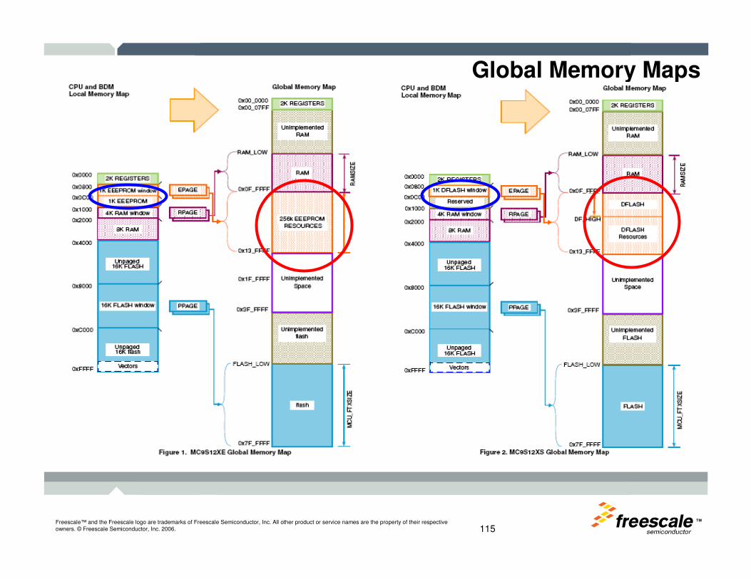
TMFreescale™ and the Freescale logo are trademarks of Freescale Semiconductor, Inc. All other product or service names are the property of their respective owners. © Freescale Semiconductor, Inc. 2006. 115
Global Memory Maps

TMFreescale™ and the Freescale logo are trademarks of Freescale Semiconductor, Inc. All other product or service names are the property of their respective owners. © Freescale Semiconductor, Inc. 2006. 116
SCI
GPIO64 LQFP, 80 QFP
48 QFN
S12P Family ►S12P Family:
� S12 core
� 32MHz bus frequency
� 180nm SGF technology
� MCG Internal oscillator
� One SCI/LIN module
� One MS-CAN Interface
� 4K DataFlash
� 48 QFN, 64 LQFP and 80 QFP
� High-speed 12-bit ATD
� 16-bit Timer with 8 IC-OC
configurable channels
� Six 8-bit PWM channels
► S12P128 Schedule :
► Target sample date: Apr08
► Target qualification date: Apr09
4K DataFlash
INT DBG
MCG
128KB Flash ECC
6KB RAM
S12CPU
ATD 12b 10ch
Timer 16b 8ch
PWM 8b 6ch
This document contains forward-looking statements based on current expectations, forecast and assumptions of Freescale that involves risk and uncertainties. Forward looking statements are subject to risk and uncertainties associated with Freescale business that could cause actual results to vary materially from those stated or implied by such forward-looking statements.
SPI
MSCAN
Device Flash RAM EE Bus Speed CAN SCI SPI TIMER Vcc PWM ADC Package (Pin)
S12P128 128K 6K 4K DataFlash 32MHz 1 1 1 8ch 16bit 3-5V 6ch 10ch 12bit 48QFN, 64LQFP, 80QFP
S12P96 96K 6K 4K DataFlash 32MHz 1 1 1 8ch 16bit 3-5V 6ch 10ch 12bit 48QFN, 64LQFP, 80QFP
S12P64 64K 4K 4K DataFlash 32MHz 1 1 1 8ch 16bit 3-5V 6ch 10ch 12bit 48QFN, 64LQFP, 80QFP
S12P32 32K 2K 4K DataFlash 32MHz 1 1 1 8ch 16bit 3-5V 6ch 10ch 12bit 48QFN, 64 LQFP
TMFreescale™ and the Freescale logo are trademarks of Freescale Semiconductor, Inc. All other product or service names are the property of their respective owners. © Freescale Semiconductor, Inc. 2006. 117
P-Family Benefits and Applications
► Product Benefits� Family Concept- S12P family scalable between 32-128K, pin-compatible with S12XS Family� CAN – 1 MSCAN module supporting CAN 2.0 A/B protocol� ECC- Industry leading flash with Error Correction Code to ensure write=read, algorithm
detects two errors corrects single error � Dataflash- for EEPROM emulation� Packaging - Small footprint QFN and LQFP packages. � 16-bit code efficiency- CISC instruction set requires less memory than comparable 32-bit
solutions � Enhanced ATD- 12-bit resolution, comparator functionality reduces CPU overhead� IPLL- frequency modulated PLL that eliminates need for off-chip components, reduces EMI� Low power consumption, Low EMC� Software/ Tool Support- Leverages established suite of hardware and software development
tools available today for the S12X Architecture
► Applications� Smart Junction Box� Seat Controller� HVAC� Low End Body ECU� RKE Receiver� Door Module� Steering Module� Low-end ABS� Watchdog Module
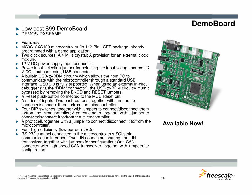
TMFreescale™ and the Freescale logo are trademarks of Freescale Semiconductor, Inc. All other product or service names are the property of their respective owners. © Freescale Semiconductor, Inc. 2006. 118
DemoBoard► Low cost $99 DemoBoard► DEMOS12XSFAME
► Features► MC9S12XS128 microcontroller (in 112-Pin LQFP package, already
programmed with a demo application).► Two clock sources: A 4 MHz crystal; A provision for an external clock
module.► 12 V DC power supply input connector.► Power input selection jumper for selecting the input voltage source: 12
V DC input connector; USB connector.► A built-in USB-to-BDM circuitry which allows the host PC to
communicate with the microcontroller through a standard USB interface. USB 2.0 is fully supported. When using an external in-circuit debugger (via the “BDM” connector), the USB-to-BDM circuitry must be bypassed by removing the BKGD and RESET jumpers.
► A Reset push-button connected to the MCU Reset pin.► A series of inputs: Two push-buttons, together with jumpers to
connect/disconnect them to/from the microcontroller.► Four DIP-switches, together with jumpers to connect/disconnect them
to/from the microcontroller; A potentiometer, together with a jumper to connect/disconnect it to/from the microcontroller.
► A photocell, together with a jumper to connect/disconnect it to/from the microcontroller.
► Four high-efficiency (low-current) LEDs ► RS-232 channel connected to the microcontroller’s SCI serial
communication interface; Two LIN connectors sharing one LIN transceiver, together with jumpers for configuration; One CAN connector with high-speed CAN transceiver, together with jumpers for configuration.
Available Now!

TM
Freescale™ and the Freescale logo are trademarks of Freescale Semiconductor, Inc. All other product or service names are the property of their respective owners. © Freescale Semiconductor, Inc. 2006.
S12P / S12XS Compatibility

TMFreescale™ and the Freescale logo are trademarks of Freescale Semiconductor, Inc. All other product or service names are the property of their respective owners. © Freescale Semiconductor, Inc. 2006. 120
S12P v S12XS Feature CompatibilityModule S12P128 S12XS256
Core CPU12-1 CPU12X-1
Interrupts Single Priority Level 7 Priority Levels
Program Flash128 Kbytes (ECC)
32data+7ECC / 512-byte erase sector256 Kbytes (ECC)
64data+8ECC / 1024-byte erase sector
Data Flash4 Kbytes (ECC)
16data+6ECC / 256-byte erase sector8 Kbytes (ECC)
16data+6ECC / 256-byte erase sector
RAM 6 Kbytes 12 Kbytes
Debug BDM + DBG BDM / xDBG
PLL FMPLL (internal filter) FMPLL (internal filter)
Oscillators 4-16MHz LCP + 1M-IRC 4-16MHz LCP
MSCAN 1 1
SPI 1 1
SCI 1 2
ADC 10-ch / 12-bit 16-ch / 12-bit
Timer 8-ch / 16-bit (TIM) 8-ch / 16-bit (TIM)
Periodic Interrupt Timer No 4-ch
PWM 6-ch / 8-bit 8-ch / 8-bit
Voltage Regulator 3.15V – 5.5V / LVD, LVI, LVR, POR / API 3.15V – 5.5V / LVD, LVI, LVR, POR / API
S12XS Superset / S12P-S12XS Difference
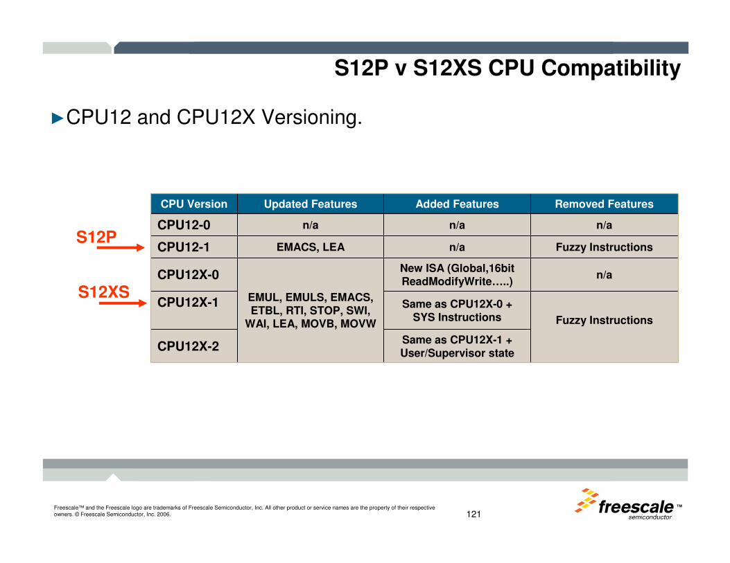
TMFreescale™ and the Freescale logo are trademarks of Freescale Semiconductor, Inc. All other product or service names are the property of their respective owners. © Freescale Semiconductor, Inc. 2006. 121
S12P v S12XS CPU Compatibility
►CPU12 and CPU12X Versioning.
CPU Version Updated Features Added Features Removed Features
CPU12-0 n/a n/a n/a
CPU12-1 EMACS, LEA n/a Fuzzy Instructions
CPU12X-0
EMUL, EMULS, EMACS, ETBL, RTI, STOP, SWI,
WAI, LEA, MOVB, MOVW
New ISA (Global,16bit ReadModifyWrite…..)
n/a
CPU12X-1 Same as CPU12X-0 + SYS Instructions Fuzzy Instructions
CPU12X-2Same as CPU12X-1 + User/Supervisor state
S12P
S12XS
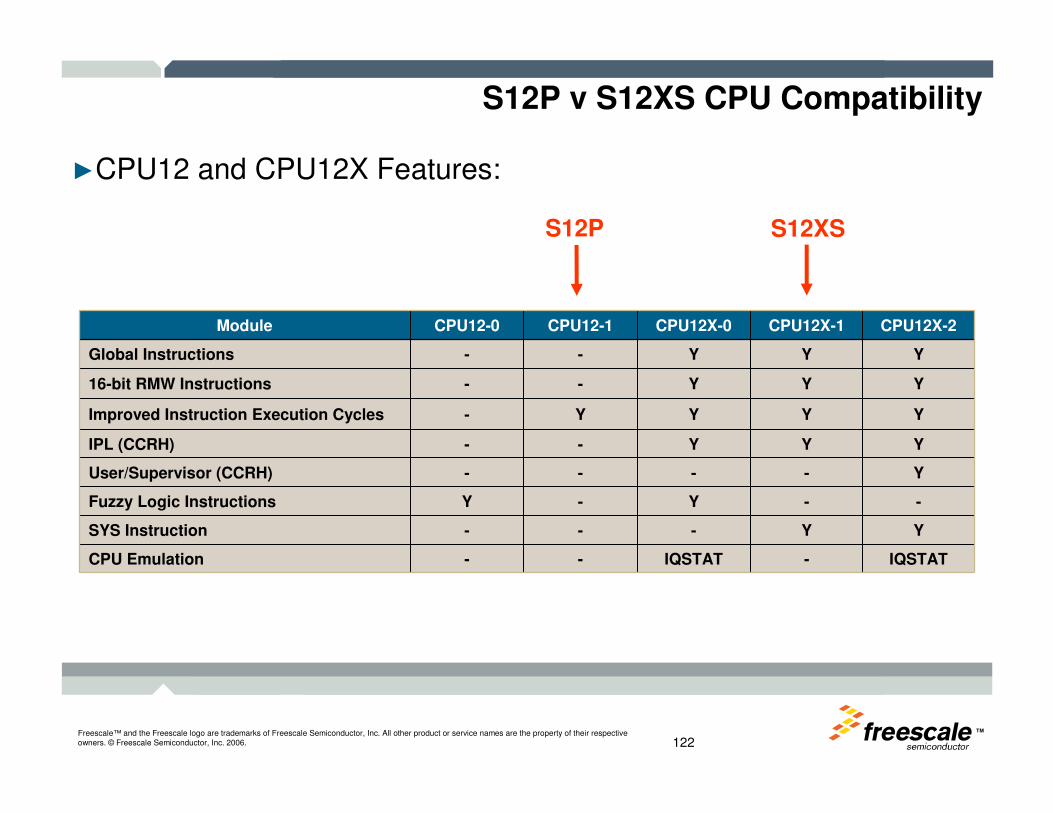
TMFreescale™ and the Freescale logo are trademarks of Freescale Semiconductor, Inc. All other product or service names are the property of their respective owners. © Freescale Semiconductor, Inc. 2006. 122
S12P v S12XS CPU Compatibility
►CPU12 and CPU12X Features:
S12P S12XS
Module CPU12-0 CPU12-1 CPU12X-0 CPU12X-1 CPU12X-2
Global Instructions - - Y Y Y
16-bit RMW Instructions - - Y Y Y
Improved Instruction Execution Cycles - Y Y Y Y
IPL (CCRH) - - Y Y Y
User/Supervisor (CCRH) - - - - Y
Fuzzy Logic Instructions Y - Y - -
SYS Instruction - - - Y Y
CPU Emulation - - IQSTAT - IQSTAT

TMFreescale™ and the Freescale logo are trademarks of Freescale Semiconductor, Inc. All other product or service names are the property of their respective owners. © Freescale Semiconductor, Inc. 2006. 123
S12P Pinout: S12XS-Compatible Version : 80QFP
► S12P eliminates 5 supply pins compared to S12XS
���� Saves 3 Bypass Caps
► Additional PH[4:0] with Key Wake-Up feature
► When soldered on an S12XS board, PH[4:0] should be configured as inputs (default at reset)
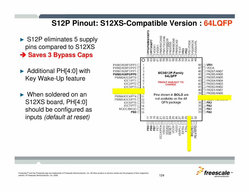
TMFreescale™ and the Freescale logo are trademarks of Freescale Semiconductor, Inc. All other product or service names are the property of their respective owners. © Freescale Semiconductor, Inc. 2006. 124
S12P Pinout: S12XS-Compatible Version : 64LQFP
► S12P eliminates 5 supply pins compared to S12XS
���� Saves 3 Bypass Caps
► Additional PH[4:0] with Key Wake-Up feature
► When soldered on an S12XS board, PH[4:0] should be configured as inputs (default at reset)
TM
S12XE Training Lab
Using CodeWarrior4.7 and DemoS12XEP100 Training Board

TM
S12XEP100 Demo Board Briefing
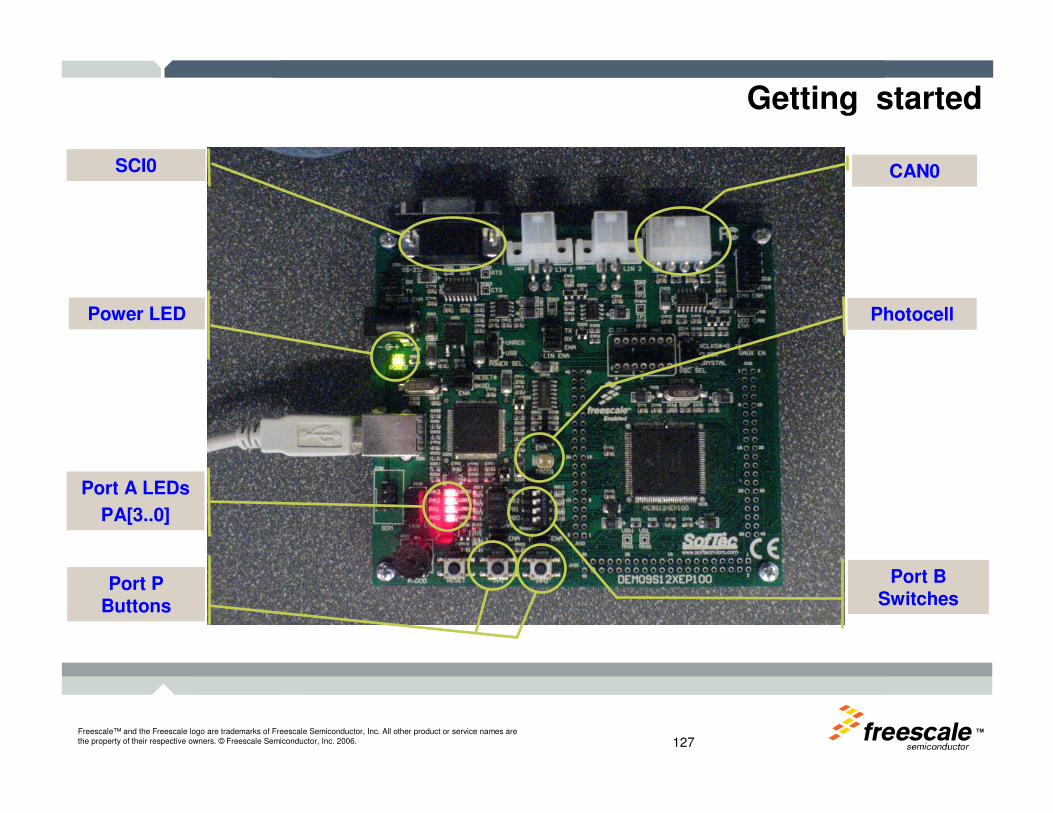
TMFreescale™ and the Freescale logo are trademarks of Freescale Semiconductor, Inc. All other product or service names are the property of their respective owners. © Freescale Semiconductor, Inc. 2006. 127
Getting started
Power LED
Port A LEDs
PA[3..0]
Port B Switches
Port P Buttons
Photocell
CAN0SCI0
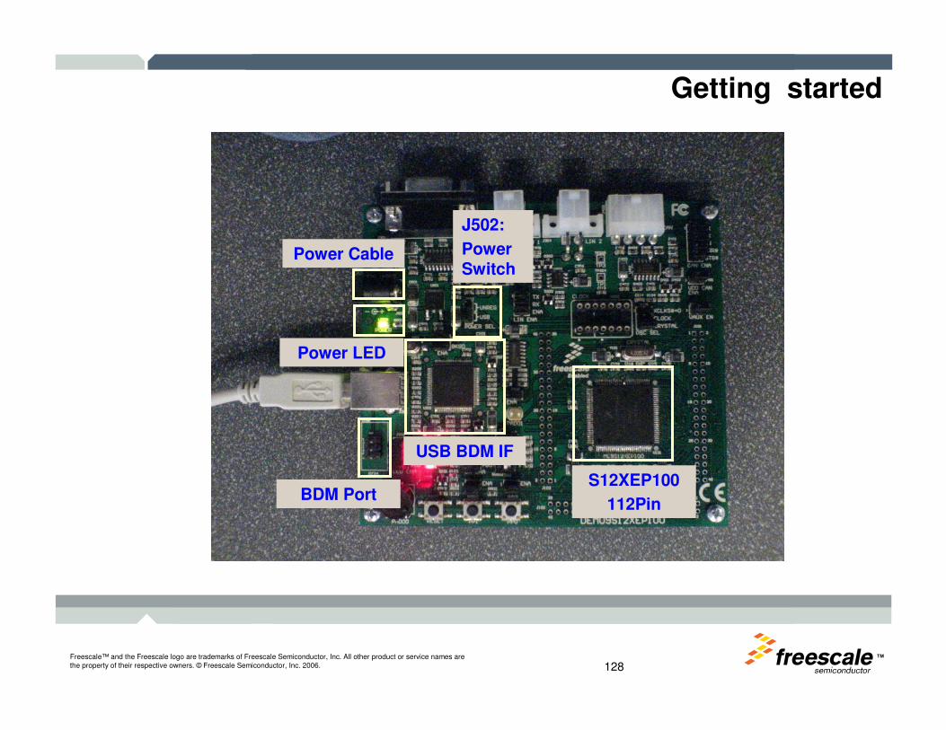
TMFreescale™ and the Freescale logo are trademarks of Freescale Semiconductor, Inc. All other product or service names are the property of their respective owners. © Freescale Semiconductor, Inc. 2006. 128
Getting started
Power LED
Power Cable
J502:
Power Switch
BDM PortS12XEP100
112Pin
USB BDM IF
TM
Freescale™ and the Freescale logo are trademarks of Freescale Semiconductor, Inc. All other product or service names are the property of their respective owners. © Freescale Semiconductor, Inc. 2006.
The First S12XE project …
TMFreescale™ and the Freescale logo are trademarks of Freescale Semiconductor, Inc. All other product or service names are the property of their respective owners. © Freescale Semiconductor, Inc. 2006. 130
In this LAB, we will:
� Get familiar with CodeWarrior 4.7 IDE;
� How to work with project wizard;
� Light the LEDs
CodeWarrior 4.7 First Simple Project
TM
Emulated EEPROM
TMFreescale™ and the Freescale logo are trademarks of Freescale Semiconductor, Inc. All other product or service names are the property of their respective owners. © Freescale Semiconductor, Inc. 2006. 132
In this LAB, we will see:
� What’s the Emulated EEPROM: nonvolatile RAM
� How to issue CCOB (Common Command Object) command
� How to Partition D-Flash
� How to enable/disable EEPROM emulation

TMFreescale™ and the Freescale logo are trademarks of Freescale Semiconductor, Inc. All other product or service names are the property of their respective owners. © Freescale Semiconductor, Inc. 2006. 133
D-Flash(e.g. 16kx22)
Memory Controller
Tag-RAM(e.g. 128x16)TAG Counter
128 x 256 bytes.
SystemBus
Buffer-RAM(e.g. 2kx16)
Hardware EEE
PROGRAM:• A write to EEE sets an
associated tag and increments a Tag counter
• The FTM clears tag and decrements Tag Counter and then stores the data.
• When Tag Counter = 0 and MGBUSY = 0 all programming is complete
READ:• ‘Read-While-Write’ supported• During a reset the NVM data
is copied back to the RAM

TMFreescale™ and the Freescale logo are trademarks of Freescale Semiconductor, Inc. All other product or service names are the property of their respective owners. © Freescale Semiconductor, Inc. 2006. 134
EEE Concept – user view
Write to EEE
Read EEE immediatelyand at any time
EEE
(subject to EEEprotection)
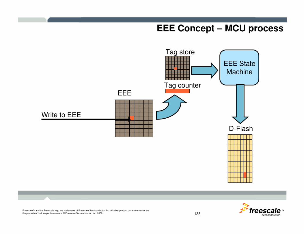
TMFreescale™ and the Freescale logo are trademarks of Freescale Semiconductor, Inc. All other product or service names are the property of their respective owners. © Freescale Semiconductor, Inc. 2006. 135
EEE Concept – MCU process
Write to EEE
EEE StateMachine
EEE
D-Flash
Tag store
Tag counter

TMFreescale™ and the Freescale logo are trademarks of Freescale Semiconductor, Inc. All other product or service names are the property of their respective owners. © Freescale Semiconductor, Inc. 2006. 136
EEE Concept – MCU process
Write to EEE
EEE StateMachine
EEE
D-Flash
Tag store
Tag counter
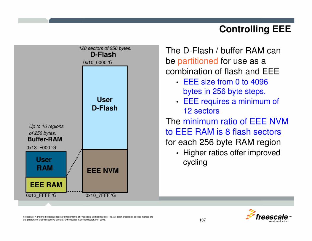
TMFreescale™ and the Freescale logo are trademarks of Freescale Semiconductor, Inc. All other product or service names are the property of their respective owners. © Freescale Semiconductor, Inc. 2006. 137
Controlling EEE
The D-Flash / buffer RAM can be partitioned for use as a combination of flash and EEE
• EEE size from 0 to 4096 bytes in 256 byte steps.
• EEE requires a minimum of 12 sectors
The minimum ratio of EEE NVM to EEE RAM is 8 flash sectorsfor each 256 byte RAM region
• Higher ratios offer improved cycling
D-Flash128 sectors of 256 bytes.
Buffer-RAM
Up to 16 regions
of 256 bytes.
EEE RAM
UserD-Flash
EEE NVM
User RAM
0x13_FFFF ‘G
0x13_F000 ‘G
0x10_0000 ‘G
0x10_7FFF ‘G
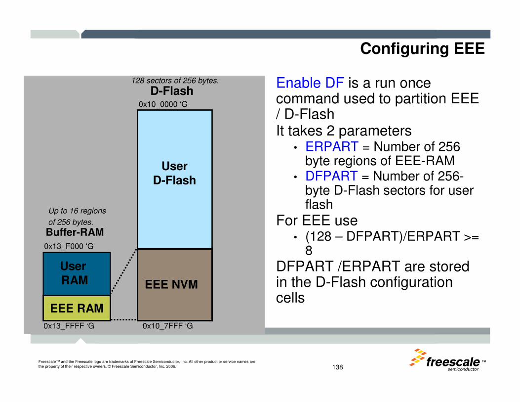
TMFreescale™ and the Freescale logo are trademarks of Freescale Semiconductor, Inc. All other product or service names are the property of their respective owners. © Freescale Semiconductor, Inc. 2006. 138
Configuring EEE
Enable DF is a run once command used to partition EEE / D-FlashIt takes 2 parameters
• ERPART = Number of 256 byte regions of EEE-RAM
• DFPART = Number of 256-byte D-Flash sectors for user flash
For EEE use • (128 – DFPART)/ERPART >=
8
DFPART /ERPART are stored in the D-Flash configuration cells
D-Flash128 sectors of 256 bytes.
Buffer-RAM
Up to 16 regions
of 256 bytes.
EEE RAM
EEE NVM
User RAM
0x13_FFFF ‘G
0x13_F000 ‘G
0x10_0000 ‘G
0x10_7FFF ‘G
UserD-Flash
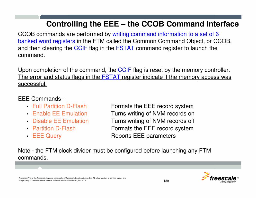
TMFreescale™ and the Freescale logo are trademarks of Freescale Semiconductor, Inc. All other product or service names are the property of their respective owners. © Freescale Semiconductor, Inc. 2006. 139
Controlling the EEE – the CCOB Command InterfaceCCOB commands are performed by writing command information to a set of 6 banked word registers in the FTM called the Common Command Object, or CCOB, and then clearing the CCIF flag in the FSTAT command register to launch the command.
Upon completion of the command, the CCIF flag is reset by the memory controller. The error and status flags in the FSTAT register indicate if the memory access was successful.
EEE Commands -
• Full Partition D-Flash Formats the EEE record system
• Enable EE Emulation Turns writing of NVM records on
• Disable EE Emulation Turns writing of NVM records off
• Partition D-Flash Formats the EEE record system
• EEE Query Reports EEE parameters
Note - the FTM clock divider must be configured before launching any FTM commands.
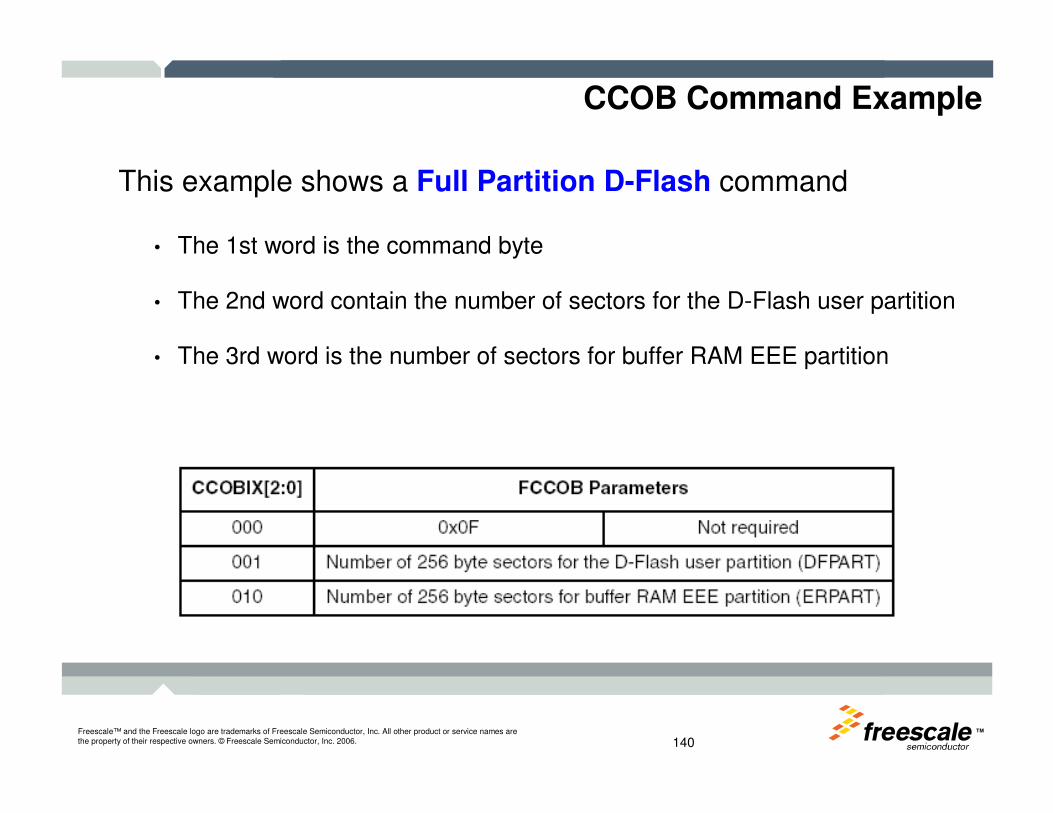
TMFreescale™ and the Freescale logo are trademarks of Freescale Semiconductor, Inc. All other product or service names are the property of their respective owners. © Freescale Semiconductor, Inc. 2006. 140
CCOB Command Example
This example shows a Full Partition D-Flash command
• The 1st word is the command byte
• The 2nd word contain the number of sectors for the D-Flash user partition
• The 3rd word is the number of sectors for buffer RAM EEE partition
TM
Freescale™ and the Freescale logo are trademarks of Freescale Semiconductor, Inc. All other product or service names are the property of their respective owners. © Freescale Semiconductor, Inc. 2006.
Memory Map LAB
TMFreescale™ and the Freescale logo are trademarks of Freescale Semiconductor, Inc. All other product or service names are the property of their respective owners. © Freescale Semiconductor, Inc. 2006. 142
MMC LAB1
Placing Data in Paged RAM and Accessing it.
How to tell the compiler that before accessing the variable, the RPAGE register must be handled.
How to declaring a pointer to tell compiler that the pointer has to be 3 bytes wide and the upper byte will contain the value of the ram page.
How to tell the compiler to initialize globle variable located in Banded space.
TMFreescale™ and the Freescale logo are trademarks of Freescale Semiconductor, Inc. All other product or service names are the property of their respective owners. © Freescale Semiconductor, Inc. 2006. 143
MMC LAB2
Allocating Big Objects
How to allocate objects bigger than the page size.
How to Use Global Accesses
TM
Freescale™ and the Freescale logo are trademarks of Freescale Semiconductor, Inc. All other product or service names are the property of their respective owners. © Freescale Semiconductor, Inc. 2006.
MPU LAB
Protecting Resources
TMFreescale™ and the Freescale logo are trademarks of Freescale Semiconductor, Inc. All other product or service names are the property of their respective owners. © Freescale Semiconductor, Inc. 2006. 145
MPU - Memory Protection Unit
The Memory Protection Unit allows users to protect memory-mapped resources from undesired access
The MPU supports multiple bus masters in the MCU• CPU, XGATE, 1 other in future, e.g. Flexray module
The MPU is always active and specifies memory ranges:• Where access is allowed and the type of access
• For each master
CPU includes additional integrated supervisor state• Allowing access to system resources
• Additional bit in CCR controls current state

TMFreescale™ and the Freescale logo are trademarks of Freescale Semiconductor, Inc. All other product or service names are the property of their respective owners. © Freescale Semiconductor, Inc. 2006. 146
MPU - Functionality
The MPU consists of a set of eight Protection Descriptors
Each descriptor defines a master, a memory range and access privileges
• There are three possible masters including the CPU which has two MPU states
• The memory range is defined by 23-bit global memory and has a resolution of 8 bytes
• Access privileges control ability to write to memory and to execute code from memory in four combinations
Each descriptor may be enabled individually
Descriptors can be configured dynamically• Typically by CPU in supervisor state during task switching

TMFreescale™ and the Freescale logo are trademarks of Freescale Semiconductor, Inc. All other product or service names are the property of their respective owners. © Freescale Semiconductor, Inc. 2006. 147
MPU - Descriptor (1)
Master select details• Four masters possible (two assigned to CPU)
• The descriptor will allow access for the specified master(s)
• Additional bit disables protection for CPU in supervisor state
LowerAddress
HigherAddress
23
Address low [22:3]
7
WP NEX
019
Address high [22:3]
MSTR Bus Master Selected
0 CPU in supervisor state
1 CPU in user state
2 XGATE
3 Other master (not used on 9S12XE100)
0 0
MSTR0
MSTR1
MSTR2
MSTR3

TMFreescale™ and the Freescale logo are trademarks of Freescale Semiconductor, Inc. All other product or service names are the property of their respective owners. © Freescale Semiconductor, Inc. 2006. 148
MPU - Descriptor (2)
Access configuration is defined by two bits in each descriptor• No Execute (NEX) and Write Protect (WP)
• Combination gives four access configurations
LowerAddress
HigherAddress
Address low [22:3]
WP NEX Address high [22:3]
WP NEX Access Example of use
0 0 Read, write, execute
Executing code from RAM
0 1 Read, write Stack and data regions
1 0 Read, execute Flash Code Region
1 1 Read Flash data region
0 0
23 7 019
MSTR0
MSTR1
MSTR2
MSTR3

TMFreescale™ and the Freescale logo are trademarks of Freescale Semiconductor, Inc. All other product or service names are the property of their respective owners. © Freescale Semiconductor, Inc. 2006. 149
MPU LAB: Using the MPU
CPU main.o is located in address range 0xFE8000 -> 0xFE8081
MPU Descriptor 1 allocates last word of this range to remainder of the flash page to No-Execute – 0xFE8080 -> 0xFEBFFF
Using the CodeWarrior HCS12X Address Mapping Tool(hcs12xadrmap.exe) confirm that this logical address range corresponds to a global address range of 0x7F8080 -> 0x7FBFFF.
RUN and note that LED 4 lights dues to MPU violation. Violation caused due to CPU fetching of program code within code area.
OBSERVE:1. Check MPUFLAG (0x0114) to confirm the type of MPU violation.
2. Verify violating address at MPUASTAT0/1/2 (0x0115-17).
ACTIONS:1. Change MPU Descriptor 1 LOW_ADDR to remove violation generated by CPU code
pre-fetch.
2. Compile and run code to ensure violation is not generated. Is LED4 illuminated?
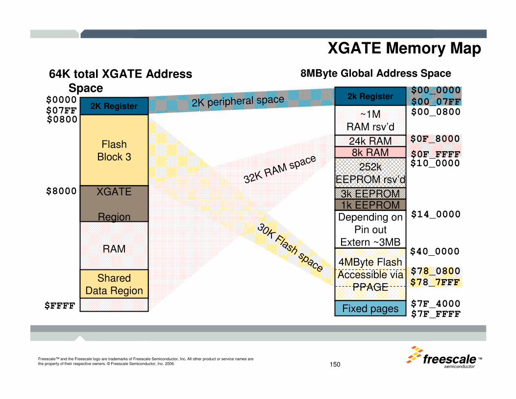
TMFreescale™ and the Freescale logo are trademarks of Freescale Semiconductor, Inc. All other product or service names are the property of their respective owners. © Freescale Semiconductor, Inc. 2006. 150
XGATE Memory Map
FlashBlock 3
RAM
$8000
$FFFF
XGATE
Region
SharedData Region
$00002K Register$07FF
$00_07FF
$0F_8000
$0F_FFFF
$0800
$78_0800$78_7FFF
64K total XGATE Address Space
8MByte Global Address Space
4MByte FlashAccessible via
PPAGE
Fixed pages$7F_FFFF
$00_0000
$10_0000
~1MRAM rsv’d
8k RAM24k RAM
252kEEPROM rsv’d
1k EEPROM3k EEPROM
2k Register
$14_0000
$00_0800
Depending onPin out
Extern ~3MB$40_0000
2K peripheral space
32K RAM space
$7F_4000
30K Flash space

TMFreescale™ and the Freescale logo are trademarks of Freescale Semiconductor, Inc. All other product or service names are the property of their respective owners. © Freescale Semiconductor, Inc. 2006. 151
CodeWarrior S12X Address Mapping Tool
FlashBlock 3
RAM
XGATE
Region
SharedData Region
2K Register
4MByte FlashAccessible via
PPAGE
Fixed pages
~1MRAM rsv’d
8k RAM24k RAM
252kEEPROM rsv’d
1k EEPROM3k EEPROM
2k Register
Depending onPin out
Extern ~3MB
2K peripheral space
32K RAM space
30K Flash space
Example 1: RAM Address Example 2: Flash Address
TM
Freescale™ and the Freescale logo are trademarks of Freescale Semiconductor, Inc. All other product or service names are the property of their respective owners. © Freescale Semiconductor, Inc. 2006.
XGATE Configuration
(SCI Demo)
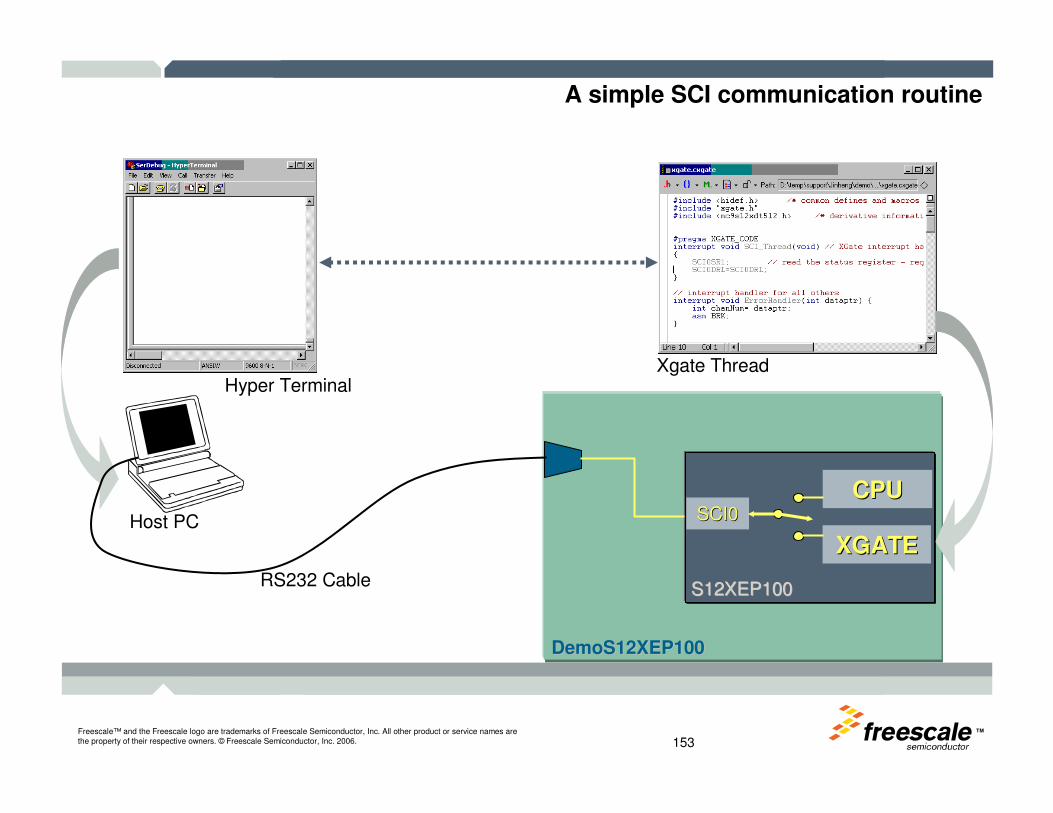
TMFreescale™ and the Freescale logo are trademarks of Freescale Semiconductor, Inc. All other product or service names are the property of their respective owners. © Freescale Semiconductor, Inc. 2006. 153
DemoS12XEP100DemoS12XEP100
CPUCPU
XGATEXGATE
S12XEP100S12XEP100
SCI0SCI0
RS232 Cable
Host PC
Hyper TerminalXgate Thread
A simple SCI communication routine

TMFreescale™ and the Freescale logo are trademarks of Freescale Semiconductor, Inc. All other product or service names are the property of their respective owners. © Freescale Semiconductor, Inc. 2006. 154
Switch SCI0 interrupt to XGATE
INT_CFADDR
1 1 0 1 0 1 1 0SCI0 Vector:0xD6
1 1 0 1 0 0 0 0
0 0 0 0 0 0 0 0
0 0 0 0 0 0 0 0
0 0 0 0 0 0 0 0
0 0 0 0 0 0 0 0
0 0 0 0 0 0 0 0
0 0 0 0 0 0 0 0
0 0 0 0 0 0 0 0
1 0 0 0 0 0 0 1
…
SPI0
SCI0
SCI1
…
XGATE INT: RQST=1
INT LEVEL: ILVL=001
#define ROUTE_INTERRUPT(vec_adr, cfdata) \
INT_CFADDR= (vec_adr) & 0xF0; \
INT_CFDATA_ARR[((vec_adr) & 0x0F) >> 1]= (cfdata)
… …
#define SCI0_VEC 0xD6 /* vector address= $xxD6 */
… …
ROUTE_INTERRUPT(SCI0_VEC, 0x81); /* RQST=1 and PRIO=1 */
INT_CFDATA_ARR[8]

TM
Freescale™ and the Freescale logo are trademarks of Freescale Semiconductor, Inc. All other product or service names are the property of their respective owners. © Freescale Semiconductor, Inc. 2006.
Periodic Interrupt Timer LAB
TMFreescale™ and the Freescale logo are trademarks of Freescale Semiconductor, Inc. All other product or service names are the property of their respective owners. © Freescale Semiconductor, Inc. 2006. 156
In this LAB, we will learn:
� How to write a XGATE thread and
� Get it to run step by step …
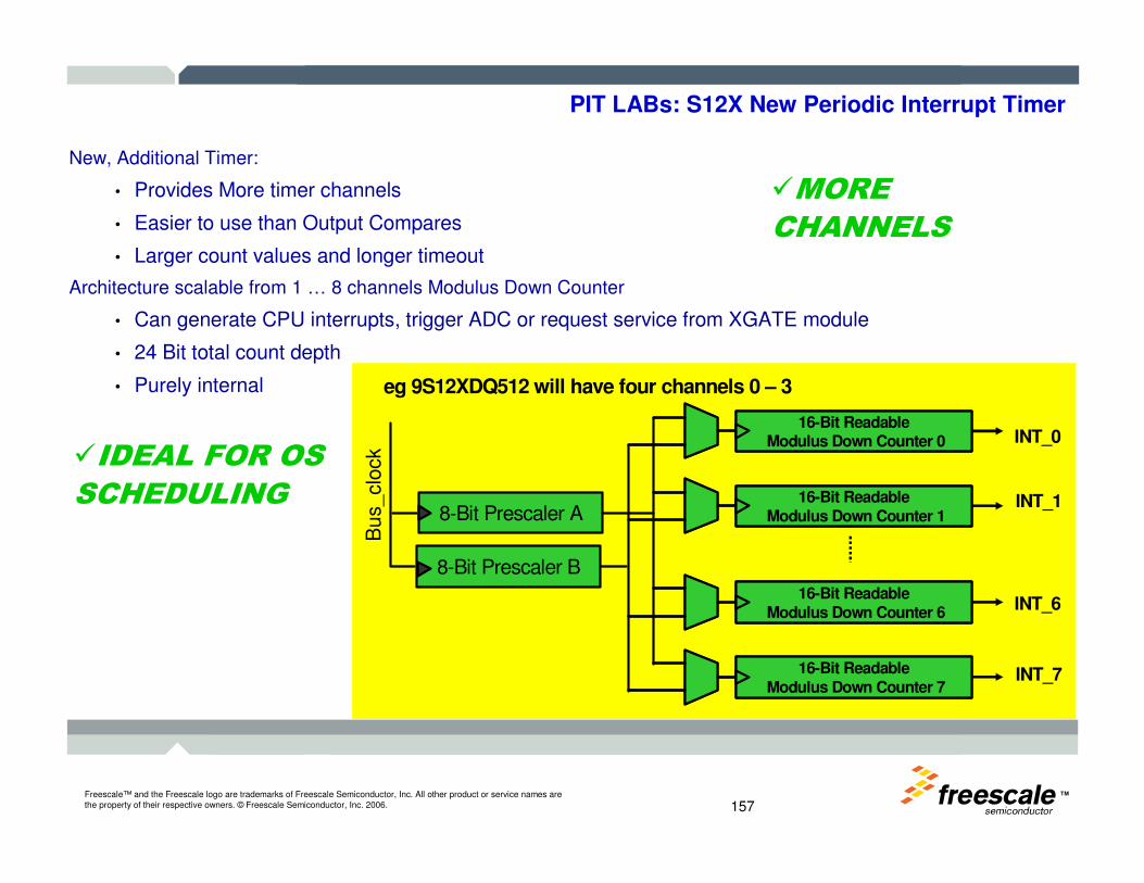
TMFreescale™ and the Freescale logo are trademarks of Freescale Semiconductor, Inc. All other product or service names are the property of their respective owners. © Freescale Semiconductor, Inc. 2006. 157
PIT LABs: S12X New Periodic Interrupt Timer
New, Additional Timer:
• Provides More timer channels
• Easier to use than Output Compares
• Larger count values and longer timeout
Architecture scalable from 1 … 8 channels Modulus Down Counter
• Can generate CPU interrupts, trigger ADC or request service from XGATE module
• 24 Bit total count depth
• Purely internal eg 9S12XDQ512 will have four channels 0 – 3
8-Bit Prescaler A
8-Bit Prescaler B
Bu
s_clo
ck
16-Bit ReadableModulus Down Counter 0
16-Bit ReadableModulus Down Counter 0 INT_0
16-Bit ReadableModulus Down Counter 7
16-Bit ReadableModulus Down Counter 7
INT_7
16-Bit ReadableModulus Down Counter 1
16-Bit ReadableModulus Down Counter 1
INT_1
16-Bit ReadableModulus Down Counter 6
16-Bit ReadableModulus Down Counter 6
INT_6
�MORE
CHANNELS
�IDEAL FOR OS
SCHEDULING
TMFreescale™ and the Freescale logo are trademarks of Freescale Semiconductor, Inc. All other product or service names are the property of their respective owners. © Freescale Semiconductor, Inc. 2006. 158
XGATE Thread Summary
1. Switch associated interrupt to XGATE and enable XGATE;
2. Write XGATE interrupt service routine (XGATE Thread);
3. Fill the XGATE thread name into the XGATE vector table
TM
Freescale™ and the Freescale logo are trademarks of Freescale Semiconductor, Inc. All other product or service names are the property of their respective owners. © Freescale Semiconductor, Inc. 2006.
XGATE Software Trigger
Mutual Function Invoke
TMFreescale™ and the Freescale logo are trademarks of Freescale Semiconductor, Inc. All other product or service names are the property of their respective owners. © Freescale Semiconductor, Inc. 2006. 160
Xgate Software triggers
In this LAB, we will learn:• How does S12XCPU invoke an XGATE function and
• How does XGATE invoke an S12XCPU function
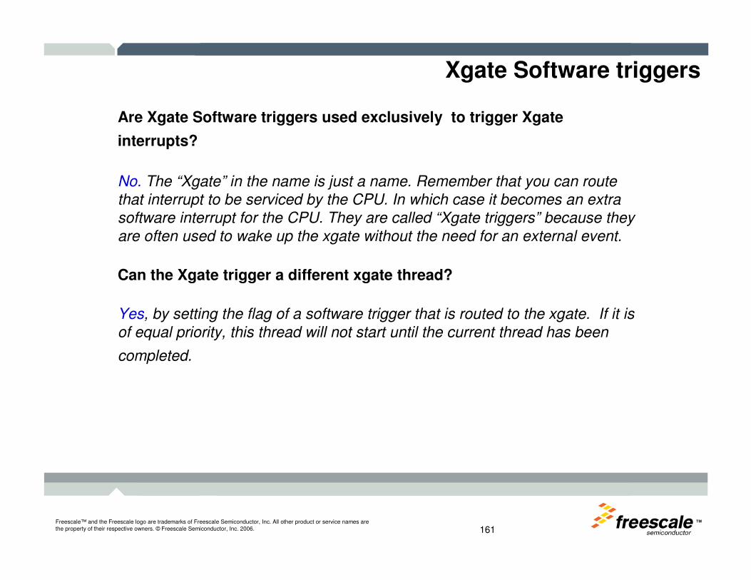
TMFreescale™ and the Freescale logo are trademarks of Freescale Semiconductor, Inc. All other product or service names are the property of their respective owners. © Freescale Semiconductor, Inc. 2006. 161
Xgate Software triggers
Are Xgate Software triggers used exclusively to trigger Xgate
interrupts?
No. The “Xgate” in the name is just a name. Remember that you can route
that interrupt to be serviced by the CPU. In which case it becomes an extra
software interrupt for the CPU. They are called “Xgate triggers” because they
are often used to wake up the xgate without the need for an external event.
Can the Xgate trigger a different xgate thread?
Yes, by setting the flag of a software trigger that is routed to the xgate. If it is
of equal priority, this thread will not start until the current thread has been
completed.

TM
Freescale™ and the Freescale logo are trademarks of Freescale Semiconductor, Inc. All other product or service names are the property of their respective owners. © Freescale Semiconductor, Inc. 2006.
Semaphore Usage
Programming for Coherency

TMFreescale™ and the Freescale logo are trademarks of Freescale Semiconductor, Inc. All other product or service names are the property of their respective owners. © Freescale Semiconductor, Inc. 2006. 163
Semaphores
The XGATE provides a set of eight hardware semaphores• Shared between the CPU and the XGATE
• Each semaphore can either be� Unlocked
� locked by the CPU
� locked by the XGATE
m m m m m m m m 1 0 1 1 0 0 0 1
Semaphores indicate the availability of shared resource
Semaphore masks allow atomic write access
unlocked
CPU
Writ
e
“1_1
”
XGATE
SSEM
CPU
Writ
e
“1_0
”XG
ATECSEM
Lockedby XGATE
Locked byS12X_CPU
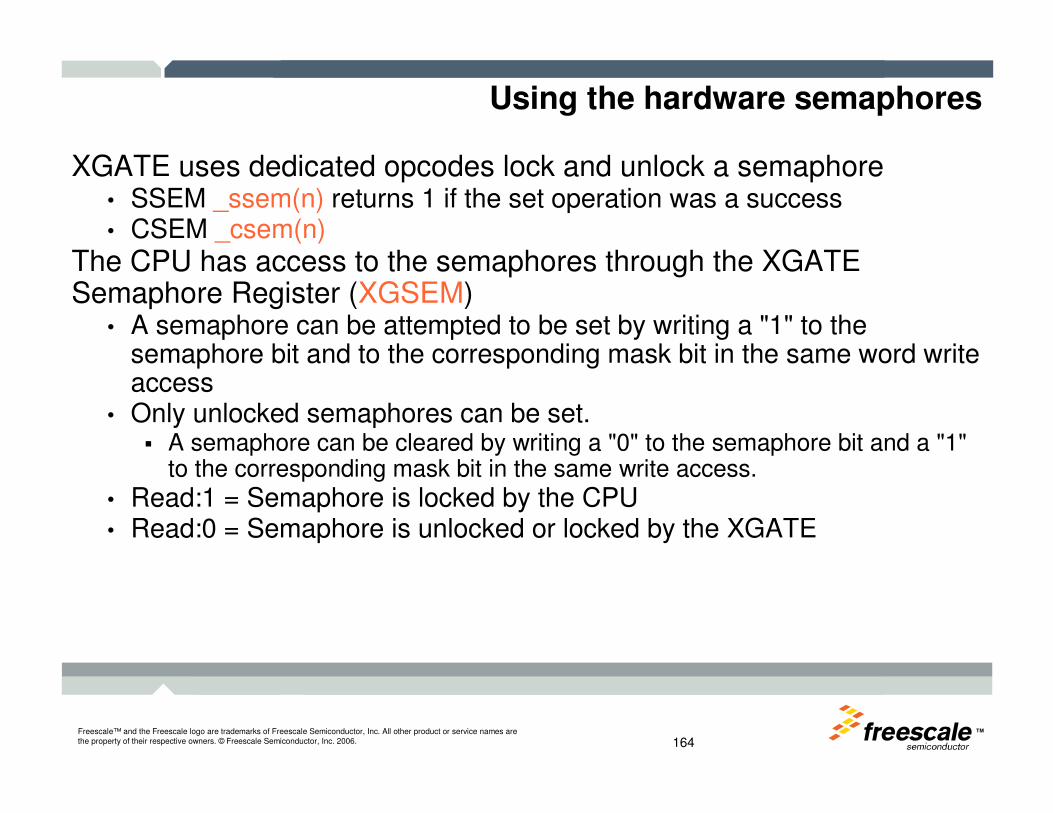
TMFreescale™ and the Freescale logo are trademarks of Freescale Semiconductor, Inc. All other product or service names are the property of their respective owners. © Freescale Semiconductor, Inc. 2006. 164
Using the hardware semaphores
XGATE uses dedicated opcodes lock and unlock a semaphore• SSEM _ssem(n) returns 1 if the set operation was a success• CSEM _csem(n)
The CPU has access to the semaphores through the XGATE Semaphore Register (XGSEM)
• A semaphore can be attempted to be set by writing a "1" to the semaphore bit and to the corresponding mask bit in the same word write access
• Only unlocked semaphores can be set.� A semaphore can be cleared by writing a "0" to the semaphore bit and a "1"
to the corresponding mask bit in the same write access.
• Read:1 = Semaphore is locked by the CPU• Read:0 = Semaphore is unlocked or locked by the XGATE
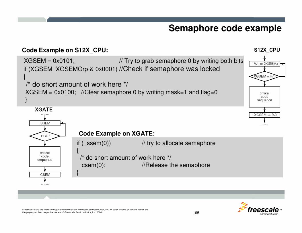
TMFreescale™ and the Freescale logo are trademarks of Freescale Semiconductor, Inc. All other product or service names are the property of their respective owners. © Freescale Semiconductor, Inc. 2006. 165
Semaphore code example
XGSEM = 0x0101; // Try to grab semaphore 0 by writing both bits
if (XGSEM_XGSEMGrp & 0x0001) //Check if semaphore was locked{
/* do short amount of work here */XGSEM = 0x0100; //Clear semaphore 0 by writing mask=1 and flag=0}
Code Example on S12X_CPU:
if (_ssem(0)) // try to allocate semaphore{/* do short amount of work here */
_csem(0); //Release the semaphore}
Code Example on XGATE:
TMFreescale™ and the Freescale logo are trademarks of Freescale Semiconductor, Inc. All other product or service names are the property of their respective owners. © Freescale Semiconductor, Inc. 2006. 166
Using semaphores
In this example you will use the hardware semaphores to manage a single resource
• Changes the button at PP0 / PP1 cause LED1..4 to toggle a pattern 4 times
• PP1 is monitored by the CPU
• PP0 is monitored by the XGATE
• Both CPU and XGATE write directly to the LEDs� Flashing 0101 - 1010 by XGATE
� Flashing 0110 - 1001 by CPU
• In the example the CPU can disrupt the XGATE pattern and vice versa
• Use semaphores to prevent this
Board-based
SEM.mcp
TMFreescale™ and the Freescale logo are trademarks of Freescale Semiconductor, Inc. All other product or service names are the property of their respective owners. © Freescale Semiconductor, Inc. 2006. 167
By using semaphores we can restrict the use of the LEDs to one core at a time
We therefore use the semaphore availability to determine if we can service the interrupt request
The CPU accesses the semaphore through the normal peripheral map
The XGATE uses its special instructions to do the same
Board-based
Using semaphores
TM
Freescale™ and the Freescale logo are trademarks of Freescale Semiconductor, Inc. All other product or service names are the property of their respective owners. © Freescale Semiconductor, Inc. 2006.
Virtual Peripherals
FullCan Driver (Demo)
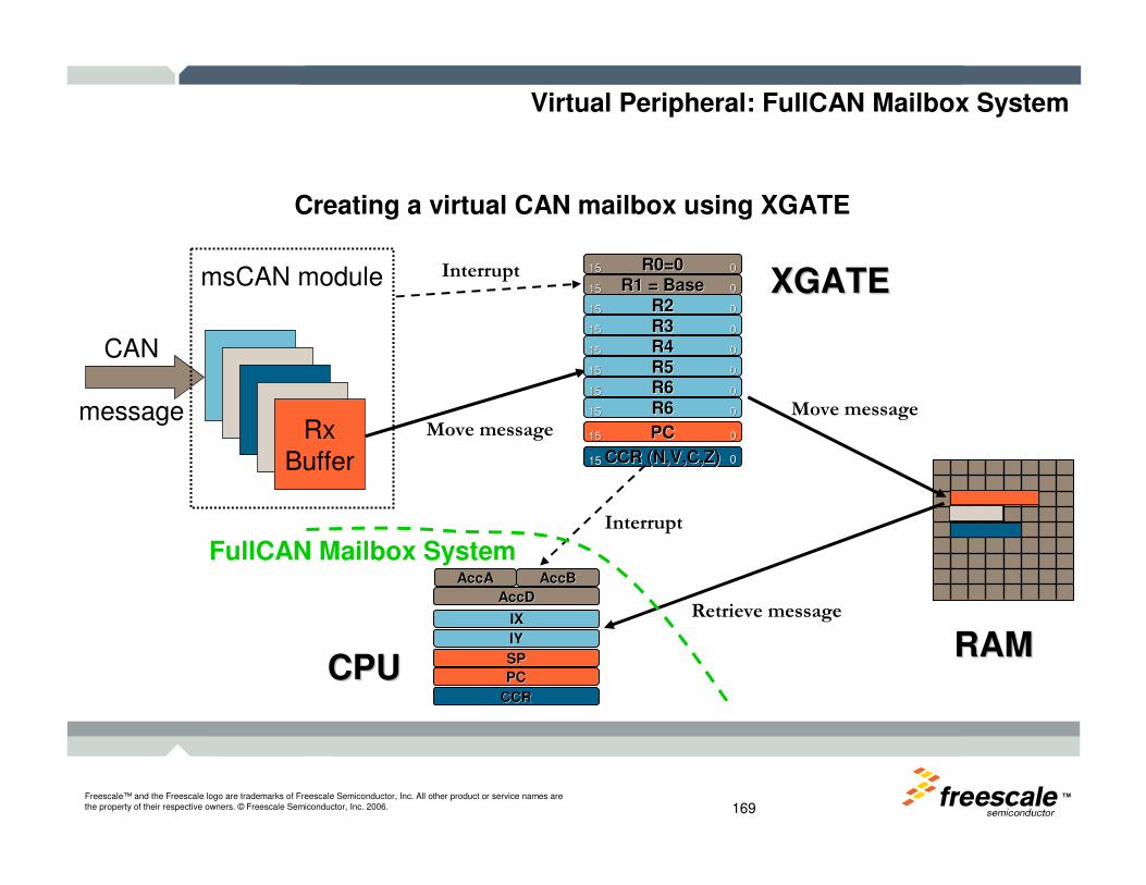
TMFreescale™ and the Freescale logo are trademarks of Freescale Semiconductor, Inc. All other product or service names are the property of their respective owners. © Freescale Semiconductor, Inc. 2006. 169
Virtual Peripheral: FullCAN Mailbox System
Creating a virtual CAN mailbox using XGATE
RxBuffer
RAMRAM
Interrupt
Move messageMove message
Interrupt
msCAN module
CCR (N,V,C,Z)CCR (N,V,C,Z) 001515
PCPC 001515
R6R6 001515
R6R6 001515
R5R5 001515
R4R4 001515
R3R3 001515
R2R2 001515
R1 = BaseR1 = Base 001515
R0=0R0=0 001515
CCRCCR
PCPC
SPSP
IYIY
IXIX
AccDAccD
AccAAccA AccBAccB
CAN
message
XGATEXGATE
CPUCPU
Retrieve message
FullCAN Mailbox System

TMFreescale™ and the Freescale logo are trademarks of Freescale Semiconductor, Inc. All other product or service names are the property of their respective owners. © Freescale Semiconductor, Inc. 2006. 170
Main purposesMain purposes::::::::Design LLD on XGATEDesign LLD on XGATE
How CPU and XGATE collaborateHow CPU and XGATE collaborate
CPUCPU
XGATEXGATE
S12XEP100S12XEP100
CAN0CAN0
MailBoxMailBox
DemoS12EP100DemoS12EP100
CAN Cable
CPUCPU
XGATEXGATE
S12XEP100S12XEP100
CAN0CAN0
MailBoxMailBox
DemoS12XEP100DemoS12XEP100
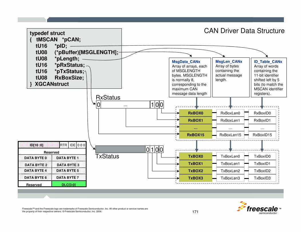
TMFreescale™ and the Freescale logo are trademarks of Freescale Semiconductor, Inc. All other product or service names are the property of their respective owners. © Freescale Semiconductor, Inc. 2006. 171
RxBOX15
…
RxBOX1
RxBOX0
RxBoxLen15
…
RxBoxLen1
RxBoxLen0
RxBoxID15
…
RxBoxID1
RxBoxID0
TxBOX3
TxBOX2
TxBOX1
TxBOX0
TxBoxLen3
TxBoxLen2
TxBoxLen1
TxBoxLen0
TxBoxID3
TxBoxID2
TxBoxID1
TxBoxID0
ID_Table_CANxArray of words containing the 11-bit identifier shifted left by 5 bits (to match the MSCAN identifier registers).
MsgData_CANxArray of arrays, each of MSGLENGTH bytes. MSGLENGTH is normally 8, corresponding to the maximum CAN message data length
MsgLen_CANxArray of bytes containing the actual message length.
typedef struct { tMSCAN *pCAN;
tU16 *pID;tU08 (*pBuffer)[MSGLENGTH]; tU08 *pLength;tU16 *pRxStatus;tU16 *pTxStatus;tU08 RxBoxSize;
} XGCANstruct
0 1 0 0TxStatus
0 1 0 0…
RxStatus
CAN Driver Data Structure
ID[10 :0] RTR IDE 0 0 0
Reserved
DATA BYTE 0 DATA BYTE 1
DATA BYTE 2 DATA BYTE 3
DATA BYTE 4 DATA BYTE 5
DATA BYTE 6 DATA BYTE 7
Reserved DLC[3:0]
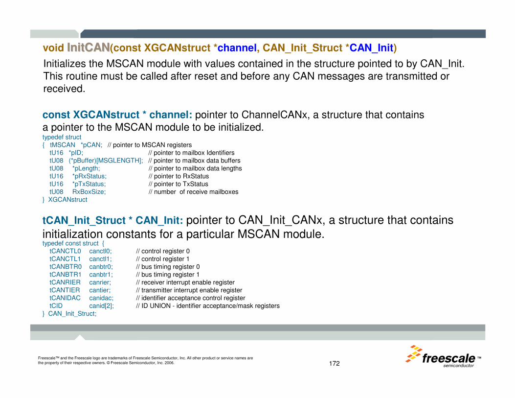
TMFreescale™ and the Freescale logo are trademarks of Freescale Semiconductor, Inc. All other product or service names are the property of their respective owners. © Freescale Semiconductor, Inc. 2006. 172
void InitCANInitCAN(const XGCANstruct *channel, CAN_Init_Struct *CAN_Init)
const XGCANstruct * channel: pointer to ChannelCANx, a structure that containsa pointer to the MSCAN module to be initialized.typedef struct { tMSCAN *pCAN; // pointer to MSCAN registers
tU16 *pID; // pointer to mailbox Identifiers tU08 (*pBuffer)[MSGLENGTH]; // pointer to mailbox data buffers tU08 *pLength; // pointer to mailbox data lengthstU16 *pRxStatus; // pointer to RxStatus tU16 *pTxStatus; // pointer to TxStatus tU08 RxBoxSize; // number of receive mailboxes
} XGCANstruct
tCAN_Init_Struct * CAN_Init: pointer to CAN_Init_CANx, a structure that contains initialization constants for a particular MSCAN module.typedef const struct {
tCANCTL0 canctl0; // control register 0 tCANCTL1 canctl1; // control register 1 tCANBTR0 canbtr0; // bus timing register 0tCANBTR1 canbtr1; // bus timing register 1tCANRIER canrier; // receiver interrupt enable register tCANTIER cantier; // transmitter interrupt enable register tCANIDAC canidac; // identifier acceptance control register tCID canid[2]; // ID UNION - identifier acceptance/mask registers
} CAN_Init_Struct;
Initializes the MSCAN module with values contained in the structure pointed to by CAN_Init. This routine must be called after reset and before any CAN messages are transmitted or received.
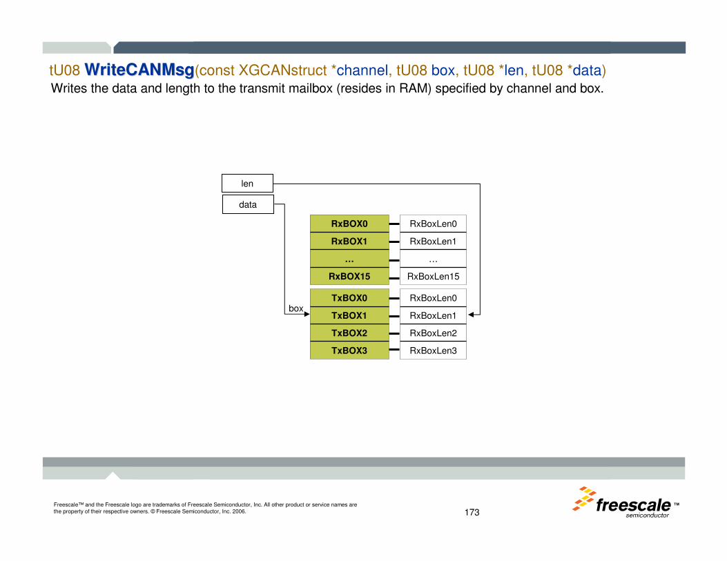
TMFreescale™ and the Freescale logo are trademarks of Freescale Semiconductor, Inc. All other product or service names are the property of their respective owners. © Freescale Semiconductor, Inc. 2006. 173
tU08 WriteCANMsgWriteCANMsg(const XGCANstruct *channel, tU08 box, tU08 *len, tU08 *data) Writes the data and length to the transmit mailbox (resides in RAM) specified by channel and box.
data
RxBOX15
…
RxBOX1
RxBOX0
TxBOX3
TxBOX2
TxBOX1
TxBOX0
RxBoxLen15
…
RxBoxLen1
RxBoxLen0
RxBoxLen3
RxBoxLen2
RxBoxLen1
RxBoxLen0
len
box

TMFreescale™ and the Freescale logo are trademarks of Freescale Semiconductor, Inc. All other product or service names are the property of their respective owners. © Freescale Semiconductor, Inc. 2006. 174
tU08 SendCANMsgSendCANMsg(const XGCANstruct *channel, tU08 box)Queues a transmit mailbox for transmission. The mailbox data is subsequently loaded into the next available MSCAN buffer by Xgate_CAN_Transmit. If more than one mailbox is queued for transmission for a particular channel, the highest numbered mailbox is loaded into the next available MSCAN buffer irrespective of the order in which the mailboxes were queued.
1) Set Tx status bit that pointed to by box
2) Enable CAN Tx interrupts
RxBOX15
…
RxBOX1
RxBOX0
TxBOX3
TxBOX2
TxBOX1
TxBOX0
RxBoxLen15
…
RxBoxLen1
RxBoxLen0
RxBoxLen3
RxBoxLen2
RxBoxLen1
RxBoxLen0
0 1 0 0TxStatus

TMFreescale™ and the Freescale logo are trademarks of Freescale Semiconductor, Inc. All other product or service names are the property of their respective owners. © Freescale Semiconductor, Inc. 2006. 175
void ReadCANMsgReadCANMsg(const XGCANstruct *channel, tU08 box, tU08 *len, tU08 *data) Reads the data and length from the specified receive mailbox. If a receive mailbox is read and the corresponding RxStatus bit is set, this bit is cleared by this routine.
RxBOX15
…
RxBOX1
RxBOX0
TxBOX3
TxBOX2
TxBOX1
TxBOX0
RxBoxLen15
…
RxBoxLen1
RxBoxLen0
RxBoxLen3
RxBoxLen2
RxBoxLen1
RxBoxLen0
0 1 0 0RxStatus
…
data
len

TMFreescale™ and the Freescale logo are trademarks of Freescale Semiconductor, Inc. All other product or service names are the property of their respective owners. © Freescale Semiconductor, Inc. 2006. 176
RxBOX15
…
RxBOX1
RxBOX0
TxBOX3
TxBOX2
TxBOX1
TxBOX0
RxBoxLen15
…
RxBoxLen1
RxBoxLen0
RxBoxLen3
RxBoxLen2
RxBoxLen1
RxBoxLen0
0 1 0 0RxStatus …
tU08 FindNewCANMsgFindNewCANMsg (const XGCANstruct *channel)
Searches RxStatus_CANx starting at the highest order bit, to find the first set bit indicating a new, unread, message.
find the first set bit
Return box=2

TMFreescale™ and the Freescale logo are trademarks of Freescale Semiconductor, Inc. All other product or service names are the property of their respective owners. © Freescale Semiconductor, Inc. 2006. 177
RxBOX15
…
RxBOX1
RxBOX0
TxBOX3
TxBOX2
TxBOX1
TxBOX0
RxBoxLen15
…
RxBoxLen1
RxBoxLen0
RxBoxLen3
RxBoxLen2
RxBoxLen1
RxBoxLen0
box=2
0 1 0 0TxStatus
tU08 CheckCANTxStatusCheckCANTxStatus(const XGCANstruct *channel, tU08 box)
Checks the status flag of the specified transmit mailbox.Return 1 if the transmit mailbox is queued for transmission and awaiting transfer to MSCAN transmit buffer.
Return 0 otherwise.
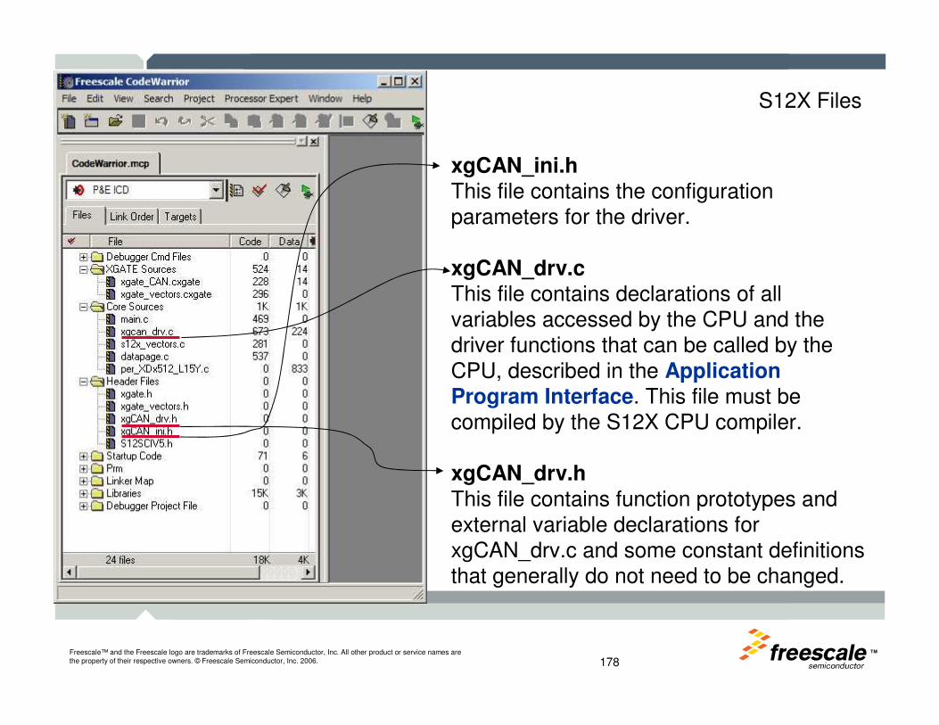
TMFreescale™ and the Freescale logo are trademarks of Freescale Semiconductor, Inc. All other product or service names are the property of their respective owners. © Freescale Semiconductor, Inc. 2006. 178
xgCAN_ini.hThis file contains the configuration parameters for the driver.
xgCAN_drv.cThis file contains declarations of all variables accessed by the CPU and the driver functions that can be called by the CPU, described in the Application Program Interface. This file must be compiled by the S12X CPU compiler.
xgCAN_drv.hThis file contains function prototypes and external variable declarations for xgCAN_drv.c and some constant definitions that generally do not need to be changed.
S12X Files
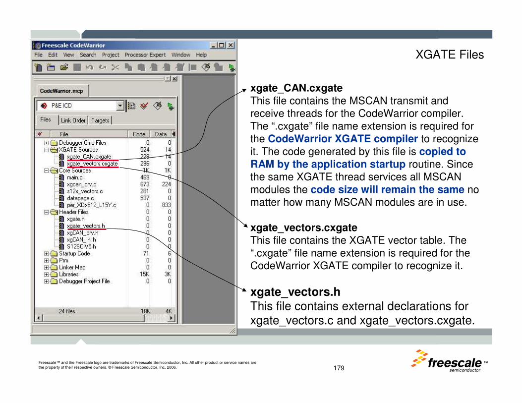
TMFreescale™ and the Freescale logo are trademarks of Freescale Semiconductor, Inc. All other product or service names are the property of their respective owners. © Freescale Semiconductor, Inc. 2006. 179
xgate_CAN.cxgateThis file contains the MSCAN transmit and receive threads for the CodeWarrior compiler. The “.cxgate” file name extension is required for the CodeWarrior XGATE compiler to recognize it. The code generated by this file is copied to RAM by the application startup routine. Since the same XGATE thread services all MSCAN modules the code size will remain the same no matter how many MSCAN modules are in use.
xgate_vectors.cxgateThis file contains the XGATE vector table. The “.cxgate” file name extension is required for the CodeWarrior XGATE compiler to recognize it.
xgate_vectors.hThis file contains external declarations for xgate_vectors.c and xgate_vectors.cxgate.
XGATE Files
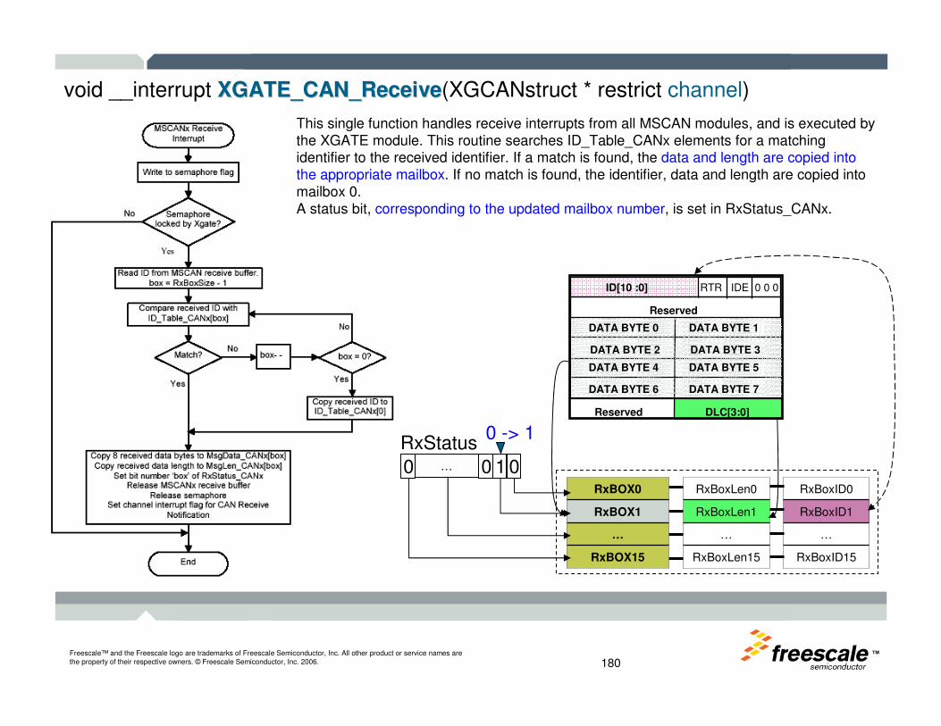
TMFreescale™ and the Freescale logo are trademarks of Freescale Semiconductor, Inc. All other product or service names are the property of their respective owners. © Freescale Semiconductor, Inc. 2006. 180
RxBOX15
…
RxBOX1
RxBOX0
RxBoxLen15
…
RxBoxLen1
RxBoxLen0
RxBoxID15
…
RxBoxID1
RxBoxID0
ID[10 :0] RTR IDE 0 0 0
Reserved
DATA BYTE 0 DATA BYTE 1
DATA BYTE 2 DATA BYTE 3
DATA BYTE 4 DATA BYTE 5
DATA BYTE 6 DATA BYTE 7
Reserved DLC[3:0]
void __interrupt XGATE_CAN_ReceiveXGATE_CAN_Receive(XGCANstruct * restrict channel)
0 0 1 0
RxStatus…
This single function handles receive interrupts from all MSCAN modules, and is executed by the XGATE module. This routine searches ID_Table_CANx elements for a matching identifier to the received identifier. If a match is found, the data and length are copied into the appropriate mailbox. If no match is found, the identifier, data and length are copied into mailbox 0.A status bit, corresponding to the updated mailbox number, is set in RxStatus_CANx.
0 -> 1
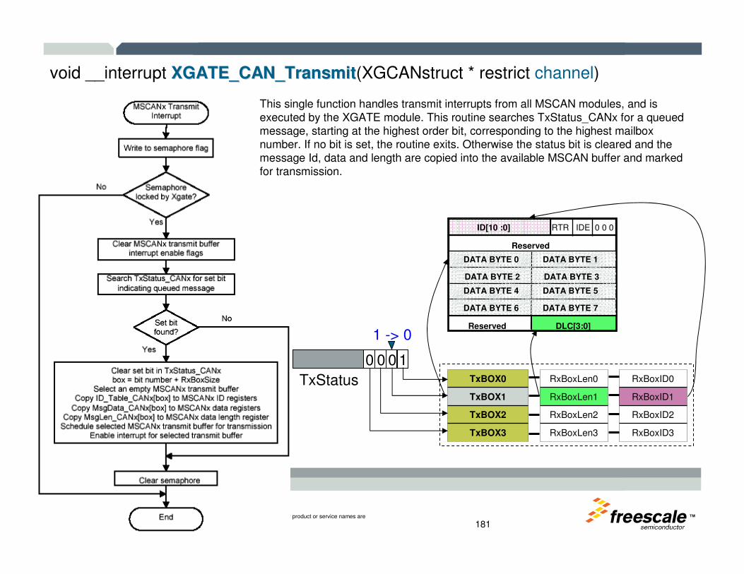
TMFreescale™ and the Freescale logo are trademarks of Freescale Semiconductor, Inc. All other product or service names are the property of their respective owners. © Freescale Semiconductor, Inc. 2006. 181
void __interrupt XGATE_CAN_TransmitXGATE_CAN_Transmit(XGCANstruct * restrict channel)
ID[10 :0] RTR IDE 0 0 0
Reserved
DATA BYTE 0 DATA BYTE 1
DATA BYTE 2 DATA BYTE 3
DATA BYTE 4 DATA BYTE 5
DATA BYTE 6 DATA BYTE 7
Reserved DLC[3:0]
TxBOX3
TxBOX2
TxBOX1
TxBOX0
RxBoxLen3
RxBoxLen2
RxBoxLen1
RxBoxLen0
RxBoxID3
RxBoxID2
RxBoxID1
RxBoxID0
0 0 0 1
TxStatus
This single function handles transmit interrupts from all MSCAN modules, and is executed by the XGATE module. This routine searches TxStatus_CANx for a queued message, starting at the highest order bit, corresponding to the highest mailbox number. If no bit is set, the routine exits. Otherwise the status bit is cleared and the message Id, data and length are copied into the available MSCAN buffer and marked for transmission.
1 -> 0
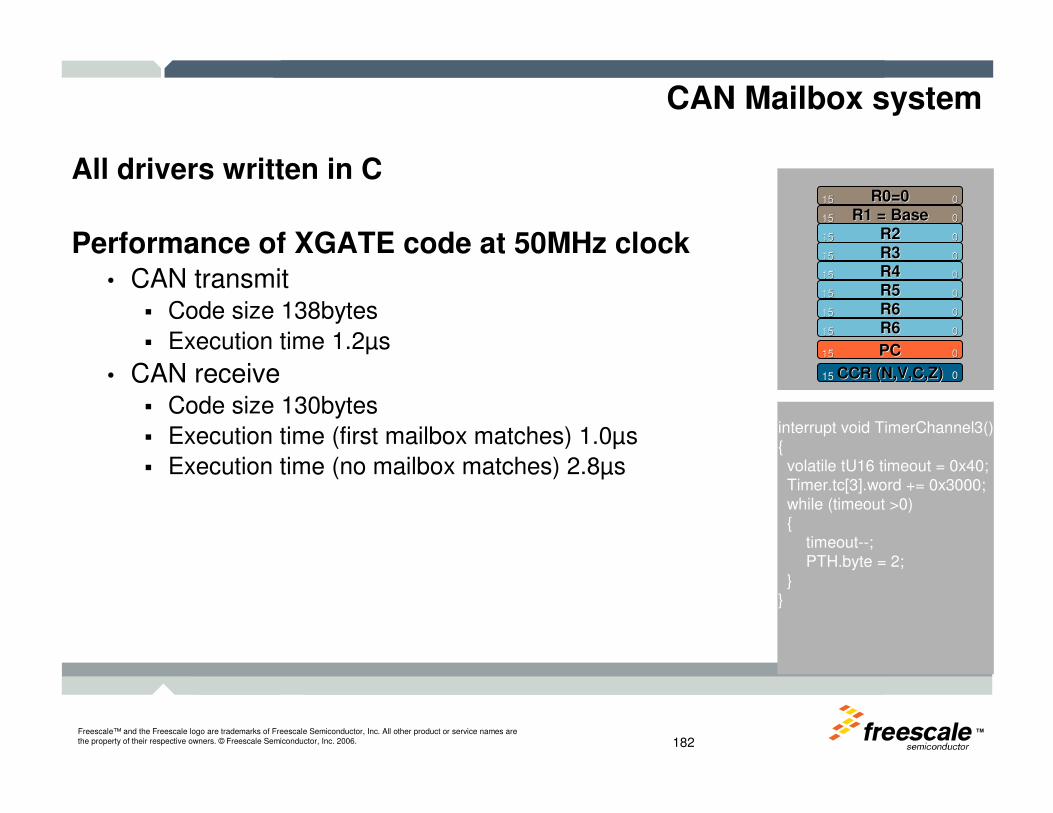
TMFreescale™ and the Freescale logo are trademarks of Freescale Semiconductor, Inc. All other product or service names are the property of their respective owners. © Freescale Semiconductor, Inc. 2006. 182
CAN Mailbox system
All drivers written in C
Performance of XGATE code at 50MHz clock• CAN transmit
� Code size 138bytes
� Execution time 1.2µs
• CAN receive� Code size 130bytes
� Execution time (first mailbox matches) 1.0µs
� Execution time (no mailbox matches) 2.8µs
interrupt void TimerChannel3(){
volatile tU16 timeout = 0x40;Timer.tc[3].word += 0x3000;while (timeout >0){
timeout--;PTH.byte = 2;
}}
CCR (N,V,C,Z)CCR (N,V,C,Z) 001515
PCPC 001515
R6R6 001515
R6R6 001515
R5R5 001515
R4R4 001515
R3R3 001515
R2R2 001515
R1 = BaseR1 = Base 001515
R0=0R0=0 001515

Freescale™ and the Freescale logo are trademarks of Freescale Semiconductor, Inc. All other product or service names are the property of their respective owners. © Freescale Semiconductor, Inc. 2005.