Embed Size (px)
Citation preview
1. General description
FXOS8700CQ is a small, low-power, 3-axis, linear accelerometer and 3-axis, magnetometer combined into a single package. The device features a selectable I2C or point-to-point SPI serial interface with 14-bit accelerometer and 16-bit magnetometer ADC resolution along with smart-embedded functions. FXOS8700CQ has dynamically selectable acceleration full-scale ranges of ±2 g/±4 g/±8 g and a fixed magnetic measurement range of ±1200 μT. Output data rates (ODR) from 1.563 Hz to 800 Hz are selectable by the user for each sensor. Interleaved magnetic and acceleration data is available at ODR rates of up to 400 Hz. FXOS8700CQ is available in a plastic QFN package and it is guaranteed to operate over the extended temperature range of –40 °C to +85 °C.
2. Features and benefits
Complete 6-axis, e-compass hardware solution
1.95 V to 3.6 V VDD supply voltage, 1.62 V to 3.6 V VDDIO voltage
±2 g/±4 g/±8 g dynamically selectable acceleration full-scale range
±1200 µT magnetic sensor full-scale range
Output data rates (ODR) from 1.563 Hz to 800 Hz for each sensor, and up to 400 Hz when operated in hybrid mode with both sensors active
Low noise: < 126 μg/√Hz acceleration noise density at 200-Hz bandwidth, < 100 nT/√Hz magnetic noise density at 100-Hz bandwidth
14-bit ADC resolution for acceleration measurements
16-bit ADC resolution for magnetic measurements
Low power: 240 μA current consumption at 100 Hz, and 80 μA at 25 Hz with both sensors active
Embedded programmable acceleration event functions
Freefall and motion detection
Transient detection
Vector-magnitude change detection
Pulse and tap detection (single and double)
Orientation detection (portrait/landscape)
Embedded programmable magnetic event functions
Threshold detection
Vector-magnitude change detection
Autonomous magnetic min/max detection
Autonomous hard-iron calibration
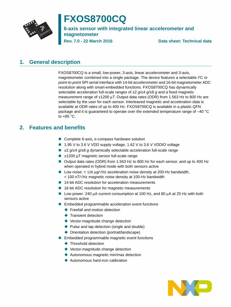
FXOS8700CQ6-axis sensor with integrated linear accelerometer and magnetometerRev. 7.0 - 22 March 2016 Data sheet: Technical data
NXP Semiconductors FXOS8700CQ6-axis sensor with integrated linear accelerometer and magnetometer
Programmable automatic ODR change using auto-wake and return-to-sleep functions to save power. This function works with both magnetic and acceleration event interrupt sources.
32-sample FIFO for acceleration data only
Integrated accelerometer self-test function
3. Applications
Security: motion detection, door opening, smart home applications, robotics, and unmanned aerial vehicles (UAVs) with electronic compass (e-compass) function.
Medical applications: patient monitoring, fall detection, and rehabilitation
E-compass in mobile devices, tablets, and personal navigation devices
User interface (menu scrolling by orientation change, tap detection for button replacement)
Orientation detection (portrait/landscape: up/down, left/right, back/front orientation identification)
Augmented reality (AR), gaming, and real-time activity analysis (pedometry, freefall, and drop detection for hard disk drives and other devices)
Power management for mobile devices using inertial and magnetic event detection
Wearable devices: motion detection, activity monitoring, sports monitoring, context awareness, and shock and vibration monitoring (mechatronic compensation, shipping, and warranty usage logging)
4. Ordering information
Table 1. Ordering information
Part number Temperature range Package description Shipping
FXOS8700CQR1 –40 °C to +85 °C QFN Tape and reel
FXOS8700CQ All information provided in this document is subject to legal disclaimers. © NXP B.V. 2016. All rights reserved.
Product data sheet Rev. 7.0 — 22 March 2016 2 of 113
NXP Semiconductors FXOS8700CQ6-axis sensor with integrated linear accelerometer and magnetometer
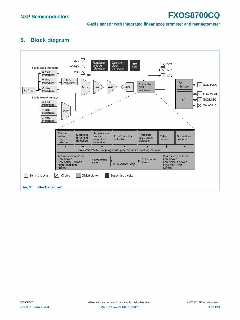
5. Block diagram
Fig 1. Block diagram
FXOS8700CQ All information provided in this document is subject to legal disclaimers. © NXP B.V. 2016. All rights reserved.
Product data sheet Rev. 7.0 — 22 March 2016 3 of 113
NXP Semiconductors FXOS8700CQ6-axis sensor with integrated linear accelerometer and magnetometer
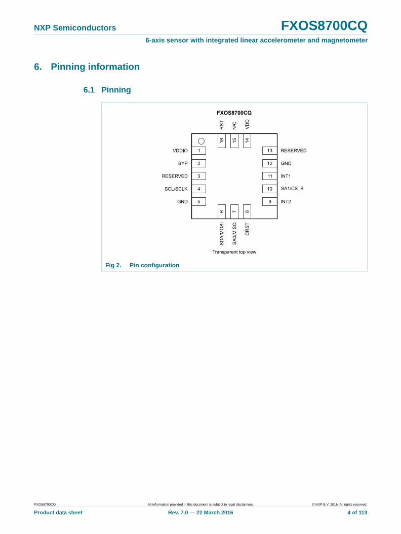
6. Pinning information
6.1 Pinning
Fig 2. Pin configuration
FXOS8700CQ All information provided in this document is subject to legal disclaimers. © NXP B.V. 2016. All rights reserved.
Product data sheet Rev. 7.0 — 22 March 2016 4 of 113
NXP Semiconductors FXOS8700CQ6-axis sensor with integrated linear accelerometer and magnetometer
6.2 Pin description
[1] Refer to Section 10.2.1 regarding point-to-point SPI operation.
[2] Refer to Section 10.2.3 regarding SPI bus requirements during 1 ms period following a reset
[3] Refer to Table 11 for I2C address options selectable using the SA0 and SA1 pins.
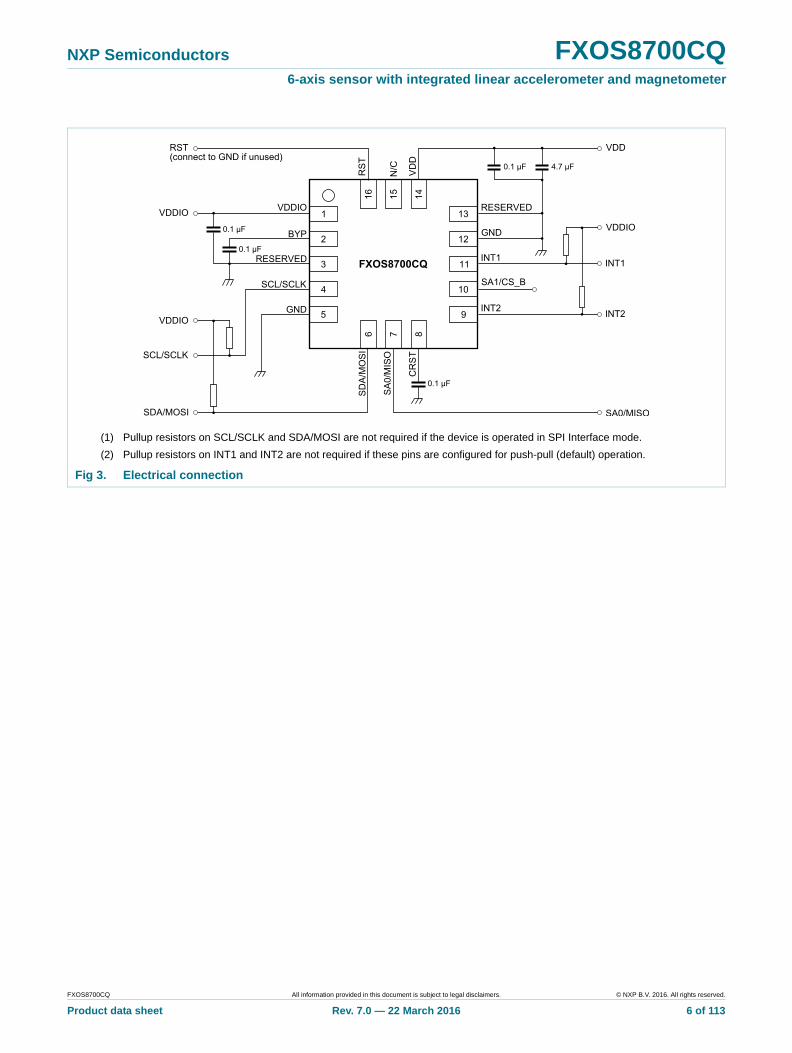
7. Electrical connections
Device power is supplied through the VDD pin. Power supply decoupling capacitors (100 nF ceramic plus 4.7 μF bulk) should be placed as close as possible to pin 14 of the device. The digital interface supply voltage (VDDIO) should be decoupled with a 100 nF ceramic capacitor placed as close as possible to pin 1 of the device.
The digital control signals SCL, SDA, SA0, SA1, and RST are not tolerant of voltages exceeding VDDIO + 0.3 V. If VDDIO is removed, these pins will clamp any logic signals through their internal ESD protection diodes. The function and timing of the two interrupt pins (INT1 and INT2) are user programmable through the I2C/SPI interface. The SDA and SCL I2C connections are open drain and therefore require a pullup resistor as shown in the application diagram in Figure 3. The INT1 and INT2 pins may also be configured for open-drain operation. If they are configured for open drain, external pullup resistors are required.
Table 2. Pin description
Symbol Pin Description
VDDIO 1 Interface supply voltage
BYP 2 Internal regulator output bypass capacitor connection
Reserved 3 Test reserved, connect to GND
SCL/SCLK 4 I2C serial clock/SPI clock[1]
GND 5 Ground
SDA/MOSI 6 I2C serial data/SPI master out, slave in[1][2]
SA0/MISO 7 I2C address selection bit 0/SPI master in, slave out[1][2][3]
Crst 8 Magnetic reset capacitor
INT2 9 Interrupt 2
SA1/CS_B 10 I2C address selection bit 1/SPI chip select (active low)[2][3]
INT1 11 Interrupt 1
GND 12 Ground
Reserved 13 Test reserved, connect to GND
VDD 14 Sensor supply voltage
N/C 15 Not connected internally
RST[2] 16 Reset input, active high. Connect to GND if unused
FXOS8700CQ All information provided in this document is subject to legal disclaimers. © NXP B.V. 2016. All rights reserved.
Product data sheet Rev. 7.0 — 22 March 2016 5 of 113
NXP Semiconductors FXOS8700CQ6-axis sensor with integrated linear accelerometer and magnetometer
(1) Pullup resistors on SCL/SCLK and SDA/MOSI are not required if the device is operated in SPI Interface mode.
(2) Pullup resistors on INT1 and INT2 are not required if these pins are configured for push-pull (default) operation.
Fig 3. Electrical connection
FXOS8700CQ All information provided in this document is subject to legal disclaimers. © NXP B.V. 2016. All rights reserved.
Product data sheet Rev. 7.0 — 22 March 2016 6 of 113
NXP Semiconductors FXOS8700CQ6-axis sensor with integrated linear accelerometer and magnetometer
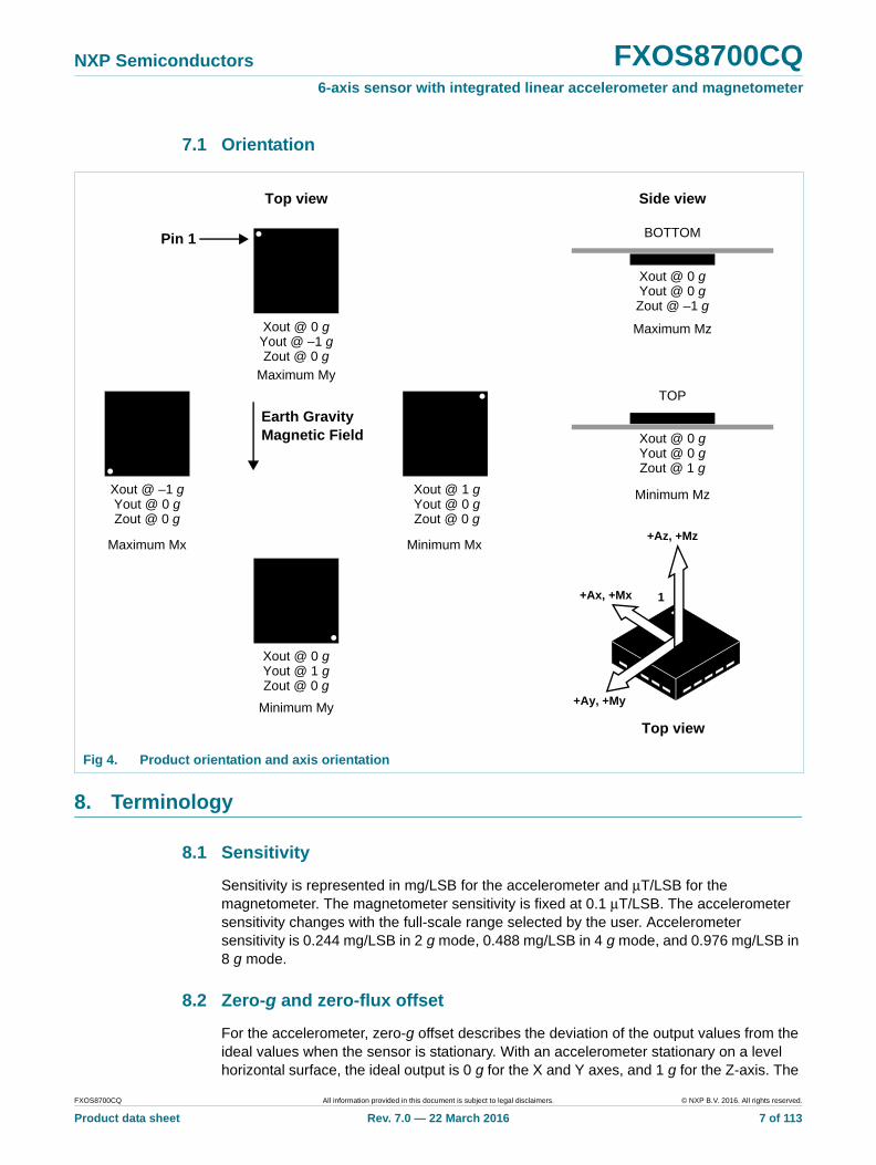
7.1 Orientation
8. Terminology
8.1 Sensitivity
Sensitivity is represented in mg/LSB for the accelerometer and μT/LSB for the magnetometer. The magnetometer sensitivity is fixed at 0.1 μT/LSB. The accelerometer sensitivity changes with the full-scale range selected by the user. Accelerometer sensitivity is 0.244 mg/LSB in 2 g mode, 0.488 mg/LSB in 4 g mode, and 0.976 mg/LSB in 8 g mode.
8.2 Zero-g and zero-flux offset
For the accelerometer, zero-g offset describes the deviation of the output values from the ideal values when the sensor is stationary. With an accelerometer stationary on a level horizontal surface, the ideal output is 0 g for the X and Y axes, and 1 g for the Z-axis. The
Fig 4. Product orientation and axis orientation
Top view
Pin 1
Side view
TOP
BOTTOM
+Ax, +Mx
+Ay, +My
+Az, +Mz
1
Top view
Xout @ 0 g
Magnetic FieldEarth Gravity
Maximum My
Minimum MxMaximum Mx
Minimum My
Maximum Mz
Minimum Mz
Yout @ –1 gZout @ 0 g
Xout @ 1 gYout @ 0 gZout @ 0 g
Xout @ –1 gYout @ 0 gZout @ 0 g
Xout @ 0 gYout @ 1 gZout @ 0 g
Xout @ 0 gYout @ 0 gZout @ 1 g
Xout @ 0 gYout @ 0 gZout @ –1 g
FXOS8700CQ All information provided in this document is subject to legal disclaimers. © NXP B.V. 2016. All rights reserved.
Product data sheet Rev. 7.0 — 22 March 2016 7 of 113
NXP Semiconductors FXOS8700CQ6-axis sensor with integrated linear accelerometer and magnetometer
deviation of each output from the ideal value is called zero-g offset. Offset is to some extent a result of stress on the sensor, and therefore, can slightly change after mounting the sensor onto a printed circuit board or exposing it to extensive mechanical stress. For the magnetometer, zero-flux offset describes the deviation of the output signals from zero when the device is shielded from external magnetic field sources (that is, inside a zero-Gauss chamber).
8.3 Self-test
Self-test can be used to verify the transducer and signal chain functionality without the need to apply an acceleration stimulus. When the accelerometer self-test is activated, an electrostatic actuation force is applied to the sensor, simulating a small acceleration. In this case the sensor X, Y, and Z outputs will exhibit a change in DC levels related to the selected full-scale range (sensitivity). When self-test is activated, the device output level is given by the algebraic sum of the signals produced by the acceleration acting on the sensor and by the electrostatic self-test force.
9. Device characteristics
9.1 Accelerometer mechanical characteristics
Table 3. Accelerometer mechanical characteristics @ VDD = 2.5 V, VDDIO = 1.8 V T = 25 °C unless otherwise noted.
Symbol Parameter Conditions Min Typ Max Unit
FSACC Measurement range ±2 g mode [1] - ±2 - g
±4 g mode - ±4 -
±8 g mode - ±8 -
SENACC Sensitivity ±2 g mode - 4096 - LSB/g
- 0.244 - mg/LSB
±4 g mode - 2048 - LSB/g
- 0.488 - mg/LSB
±8 g mode - 1024 - LSB/g
- 0.976 - mg/LSB
TCSACC Sensitivity change with temperature
±2 g, ±4 g, ±8 g modes [1] - ±0.01 - %/°C
SEN-TOLACC Sensitivity accuracy - ±2.5 - %SENACC
OFFACC Zero-g level offset accuracy ±2 g, ±4 g, ±8 g modes [2] - ±20 - mg
OFFACC-PBM Zero-g level offset accuracy post-board mount
±2 g, ±4 g, ±8 g modes [4] - ±30 - mg
TCOACC Zero-g level change versus temperature
–40 °C to 85 °C [1] - ±0.2 - mg/°C
NLACC Nonlinearity (deviation from straight line)
Over ±1 g range normal mode
[5][6] - ±0.5 - %FSACC
STOCACC Self-test output change
±2 g mode, X-axis
±2 g mode, Y-axis
±2 g mode, Z-axis
[7]
+192
+270
+1275
-
-
-
-
-
-
LSB
FXOS8700CQ All information provided in this document is subject to legal disclaimers. © NXP B.V. 2016. All rights reserved.
Product data sheet Rev. 7.0 — 22 March 2016 8 of 113
NXP Semiconductors FXOS8700CQ6-axis sensor with integrated linear accelerometer and magnetometer
[1] Dynamic range is limited to ±4 g when in the low-noise mode.
[2] Before board mount.
[3] Post-board mount offset specifications are based on a 2-layer PCB design.
[4] Evaluation only.
[5] After post-board mount corrections for sensitivity, cross axis and offset. Refer to NXP application note AN4399 for more information.
[6] Self-test is only exercised along one direction for each sensitive axis.
[7] Measured using earth's gravitational field (1 g) with the device oriented horizontally (+Z axis up) and stationary.
9.2 Magnetometer magnetic characteristics
[1] After m-cell has been factory trimmed.
[2] Hysteresis is measured by sweeping the applied magnetic field from –1000 μT to 1000 μT and then back to –1000 μT. The difference in the two readings at –1000 μT divided by the swept field range is the hysteresis figure, expressed in % of the full-scale range (FSMAG).
[3] Tested over a ±1000 μT measurement range.
NDACC Output noise density, normal mode
ODR = 400 Hz, normal mode
[4][7] - 126 - µg/√Hz
ODR = 400 Hz, low-noise mode
[1] - 99 - µg/√Hz
TOP Operating temperature range –40 - +85 °C
Table 3. Accelerometer mechanical characteristics @ VDD = 2.5 V, VDDIO = 1.8 V T = 25 °C unless otherwise noted. - ¶continued
Symbol Parameter Conditions Min Typ Max Unit
Table 4. Magnetometer magnetic characteristics @ VDD = 2.5 V, VDDIO = 1.8 V T = 25 °C unless otherwise noted.
Symbol Parameter Conditions Min Typ Max Unit
FSMAG Measurement range - ±1200 - - μT
SENMAG Sensitivity - - 0.1 - μT/LSB
TCSMAG Sensitivity change versus temperature - - ±0.1 - %/°C
OFFMAG Zero-flux offset accuracy - [1] - ±10 - μT
TCOMAG Zero-flux offset change with temperature - - ±0.8 - μT/°C
HYSTMAG Hysteresis - [2][3] - ±0.5 - %FSMAG
NLMAG Nonlinearity
Deviation from best-fit straight line -
[3]
- ±1 - %FSMAG
- Temperature sensor sensitivity - - 0.96 - °C/LSB
NoiseMAG Magnetometer output noise ODR = 800 Hz, OSR = 2 - 1.5 - μT-rms
ODR = 400 Hz, OSR = 4 - 1.2 -
ODR = 200 Hz, OSR = 8 - 0.85 -
ODR = 100 Hz, OSR = 16 - 0.6 -
ODR = 50 Hz, OSR = 32 - 0.5 -
ODR = 12.5 Hz, OSR = 128 - 0.35 -
ODR = 6.25 Hz, OSR = 256 - 0.3 -
ODR = 1.56 Hz, OSR = 1024 - 0.3 -
TOP Operating temperature range - –40 - +85 °C
FXOS8700CQ All information provided in this document is subject to legal disclaimers. © NXP B.V. 2016. All rights reserved.
Product data sheet Rev. 7.0 — 22 March 2016 9 of 113
NXP Semiconductors FXOS8700CQ6-axis sensor with integrated linear accelerometer and magnetometer
9.3 Hybrid characteristics
9.4 Electrical characteristics
Table 5. Hybrid characteristics @ VDD = 2.5 V, VDDIO = 1.8 V T = 25 °C unless otherwise noted.
Symbol Rating Value Unit Symbol Rating
ODRmax Maximum output data rate in hybrid mode - 400 - Hz
TOP Operating temperature range –40 - +85 °C
BW Output data bandwidth - ODR/2 - Hz
Table 6. Electrical characteristics @ VDD = 2.5 V, VDDIO = 1.8 V T = 25 °C unless otherwise noted.
Symbol Parameter Conditions Min Typ Max Unit
VDD Supply voltage - 1.95 2.5 3.6 V
VDDIO Interface supply voltage
- 1.62 1.8 3.6 V
IDDACC-LPM Supply current Low-power acceleration mode µA
ODR = 12.5 Hz - 8 -
ODR = 100 Hz - 35 -
ODR = 400 Hz - 130 -
IDDACC-NM Supply current Normal acceleration mode µA
ODR = 50 Hz - 35 -
ODR = 200 Hz - 130 -
ODR = 800 Hz - 240 -
IDDACC+MAG Supply current Hybrid mode μA
ODR = 200 Hz
Accelerometer OSR = 4
Magnetometer OSR = 2
- 440 -
ODR = 100 Hz
Accelerometer OSR = 4
Magnetometer OSR = 2
- 240 -
ODR = 25 Hz
Accelerometer OSR = 4
Magnetometer OSR = 2
- 80 -
IDDMAG Supply current Magnetic mode μA
ODR = 400 Hz, OSR = 2 - 575 -
ODR = 12.5 Hz, OSR = 2 - 40 -
IDDBOOT Supply current during boot sequence
0.9 ms max duration using recommended regulator bypass capacitor, VDD = 2.5 V
- - - 3
CBYP, CRST Value of capacitors on BYP and magnetic reset pins
–40 °C to 85 °C 75 100 470 nF
IDDSTBY Supply current Standby mode @ 25 °C - 2 - µA
IDDSTBY Supply current Over-temperature range, standby mode
- - 10 µA
FXOS8700CQ All information provided in this document is subject to legal disclaimers. © NXP B.V. 2016. All rights reserved.
Product data sheet Rev. 7.0 — 22 March 2016 10 of 113
NXP Semiconductors FXOS8700CQ6-axis sensor with integrated linear accelerometer and magnetometer
[1] Time from VDDIO on and VDD > VDD min until I2C/SPI interface ready for operation.
[2] Time to obtain valid data from power-down mode to active mode.
[3] Time to obtain valid data from standby mode to active mode.
VIHRST Digital high-level input voltage, RST pin
- 1.04 - - V
VILRST Digital low-level input voltage, RST pin
- - - 0.68 V
VIH Digital high-level input voltage, SCL, SDA, SA0, and SA1 pins
- 0.75*VDDIO - - V
VIL Digital low-level input voltage, SCL, SDA, SA0, and SA1 pins
- - - 0.3*VDDIO V
VOH High-level output voltage, INT and INT2 pins
IO = 500 µA 0.9*VDDIO - - V
VOL Low-level output voltage, INT1 and INT2 pins
IO = 500 µA - - 0.1*VDDIO V
VOLSDA Low-level output voltage, SDA pin
IO = 500 µA - - 0.1*VDDIO V
SCL and SDA pin leakage
25 °C - 1.0 - nA
–40 °C to 85 °C - 4.0 -
SCL and SDA pin capacitance
- - 3 - pf
VDD rise time - 0.001 - 1000 ms
TBOOT Boot time - [1] - - 1000 µs
TPOR→ACT Turn-on time 1 - [2] - 2/ODR + 2 - ms
TSTBY→ACT Turn-on time 2 - [3] - 2/ODR + 1 - ms
TOP Operating temperature range
- –40 - +85 °C
Table 6. Electrical characteristics @ VDD = 2.5 V, VDDIO = 1.8 V T = 25 °C unless otherwise noted. - ¶continued -
Symbol Parameter Conditions Min Typ Max Unit
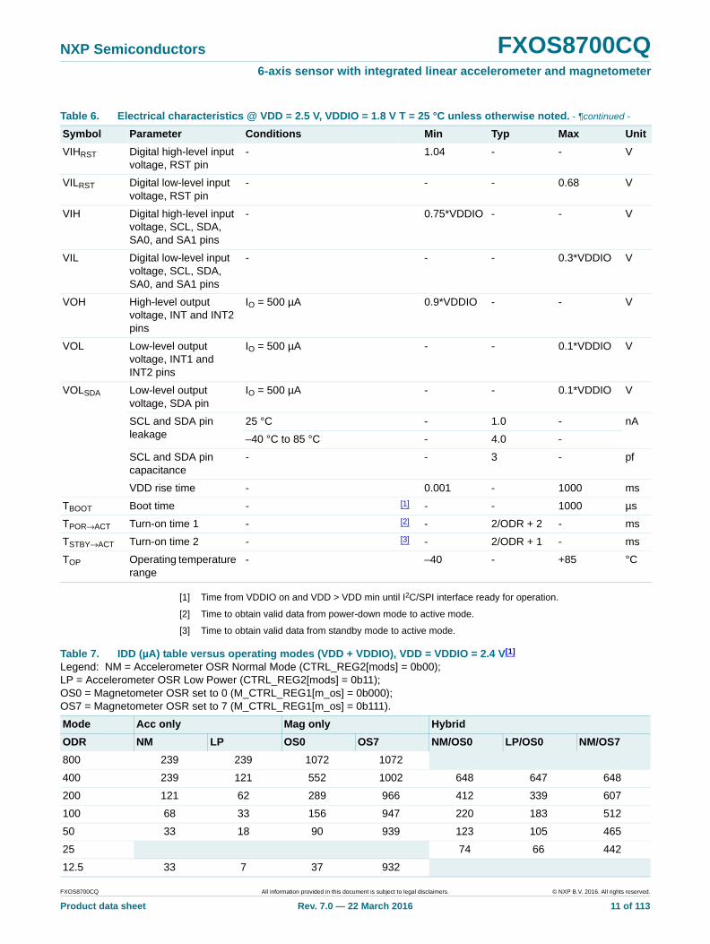
Table 7. IDD (µA) table versus operating modes (VDD + VDDIO), VDD = VDDIO = 2.4 V[1]
Legend: NM = Accelerometer OSR Normal Mode (CTRL_REG2[mods] = 0b00); LP = Accelerometer OSR Low Power (CTRL_REG2[mods] = 0b11); OS0 = Magnetometer OSR set to 0 (M_CTRL_REG1[m_os] = 0b000); OS7 = Magnetometer OSR set to 7 (M_CTRL_REG1[m_os] = 0b111).
Mode Acc only Mag only Hybrid
ODR NM LP OS0 OS7 NM/OS0 LP/OS0 NM/OS7
800 239 239 1072 1072
400 239 121 552 1002 648 647 648
200 121 62 289 966 412 339 607
100 68 33 156 947 220 183 512
50 33 18 90 939 123 105 465
25 74 66 442
12.5 33 7 37 932
FXOS8700CQ All information provided in this document is subject to legal disclaimers. © NXP B.V. 2016. All rights reserved.
Product data sheet Rev. 7.0 — 22 March 2016 11 of 113
NXP Semiconductors FXOS8700CQ6-axis sensor with integrated linear accelerometer and magnetometer
[1] Values are based on limited number of samples and are for reference only. Output data rates do not exist for the shaded cells.
9.5 Absolute maximum ratings
Stresses above those listed as “absolute maximum ratings” may cause permanent damage to the device. This is a stress rating only and functional operation of the device under these conditions is not implied. Exposure to maximum rating conditions for extended periods may affect device reliability.
NXP recommends that customers using magnetic sensor components adopt industry standard safe handling practices and procedures for magnetic products. To avoid potential damage to the magnetic transducer contained within this product, it is recommended to only handle the device with non-magnetic tools and fixtures.
[1] Sensor characteristics can be restored on a “permed” device by means of briefly applying an external uniform magnetic field on the order of 100 Gauss or greater, along the X-axis.
6.25 33 7 37 931 51 35 437
3.125 51 35 437
1.5625 33 7 36 931
0.78125 51 35 436
stby 2
Table 7. IDD (µA) table versus operating modes (VDD + VDDIO), VDD = VDDIO = 2.4 V[1] - ¶continuedLegend: NM = Accelerometer OSR Normal Mode (CTRL_REG2[mods] = 0b00); LP = Accelerometer OSR Low Power (CTRL_REG2[mods] = 0b11); OS0 = Magnetometer OSR set to 0 (M_CTRL_REG1[m_os] = 0b000); OS7 = Magnetometer OSR set to 7 (M_CTRL_REG1[m_os] = 0b111).
Mode Acc only Mag only Hybrid
ODR NM LP OS0 OS7 NM/OS0 LP/OS0 NM/OS7
Table 8. Maximum ratings
Symbol Rating Value Unit
gmax Maximum acceleration (all axes, 100 μs) 10 000 g
VDDmax Supply voltage, interface supply voltage –0.3 to +3.6 V
VDDIOmax Supply voltage, IO voltage –0.3 to +3.6 V
VINmax Input voltage on any control pin (SA0/MISO, SA1/CS_B, SCL/SCLK, SDA/MOSI, RST)
–0.3 to VDDIO + 0.3 V
Ddrop Drop-test height 1.8 m
- Maximum exposed magnetic field without perming [1] 3000 μT
- Maximum exposed field without permanent damage 0.1 T
TSTG Storage temperature range –40 to +125 °C
Table 9. ESD and latchup protection characteristics
Symbol Rating Value Unit
HBM Human body model ±2000 V
MM Machine model ±200 V
FXOS8700CQ All information provided in this document is subject to legal disclaimers. © NXP B.V. 2016. All rights reserved.
Product data sheet Rev. 7.0 — 22 March 2016 12 of 113
NXP Semiconductors FXOS8700CQ6-axis sensor with integrated linear accelerometer and magnetometer
10. Digital interfaces
10.1 I2C interface characteristics
[1] All values referred to VIH (min) and VIL (max) levels
[2] This device does not stretch the low period (tLOW) of the SCL signal.
[3] tVD;DAT = time for data signal from SCL low to SDA output.
[4] tVD;ACK = time for acknowledgement signal from SCL low to SDA output (high or low, depending on which one is worse)
[5] Cb = total capacitance of one bus line in pF.
CDM Charge device model ±500 V
ILU Latchup current at T = 85 °C ±100 mA
Table 9. ESD and latchup protection characteristics - ¶continued
Symbol Rating Value Unit
This device is sensitive to mechanical shock. Improper handling can cause permanent damage to the part or cause the part to otherwise fail.
This device is sensitive to ESD, improper handling can cause permanent damage to the part.
Table 10. I2C slave timing values[1]
Symbol Parameter I2C fast mode Unit
Min Max
fSCL SCL clock frequency 0 400 kHz
tBUF Bus free time between stop and start condition 1.3 - μs
tHD;STA (Repeated) start hold time 0.6 - μs
tSU;STA (Repeated) start setup time 0.6 - μs
tSU;STO STOP condition setup time 0.6 - μs
tHD;DAT SDA data hold time [2] 0.05 0.9 μs
tVD;DAT SDA valid time [2][3] - 0.9 μs
tVD;ACK SDA valid acknowledge time [2][4] - 0.9 μs
tSU;DAT SDA setup time 100 - ns
tLOW SCL clock low time 1.3 - μs
tHIGH SCL clock high time 0.6 - μs
tr SDA and SCL rise time [5] 20 + 0.1 Cb 300 ns
tf SDA and SCL fall time [5] 20 + 0.1 Cb 300 ns
tSP Pulse width of spikes on SDA and SCL that must be suppressed by internal input filter
0 50 ns
FXOS8700CQ All information provided in this document is subject to legal disclaimers. © NXP B.V. 2016. All rights reserved.
Product data sheet Rev. 7.0 — 22 March 2016 13 of 113
NXP Semiconductors FXOS8700CQ6-axis sensor with integrated linear accelerometer and magnetometer
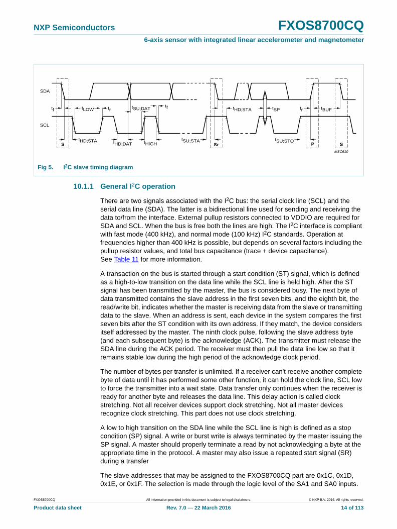
10.1.1 General I2C operation
There are two signals associated with the I2C bus: the serial clock line (SCL) and the serial data line (SDA). The latter is a bidirectional line used for sending and receiving the data to/from the interface. External pullup resistors connected to VDDIO are required for SDA and SCL. When the bus is free both the lines are high. The I2C interface is compliant with fast mode (400 kHz), and normal mode (100 kHz) I2C standards. Operation at frequencies higher than 400 kHz is possible, but depends on several factors including the pullup resistor values, and total bus capacitance (trace + device capacitance). See Table 11 for more information.
A transaction on the bus is started through a start condition (ST) signal, which is defined as a high-to-low transition on the data line while the SCL line is held high. After the ST signal has been transmitted by the master, the bus is considered busy. The next byte of data transmitted contains the slave address in the first seven bits, and the eighth bit, the read/write bit, indicates whether the master is receiving data from the slave or transmitting data to the slave. When an address is sent, each device in the system compares the first seven bits after the ST condition with its own address. If they match, the device considers itself addressed by the master. The ninth clock pulse, following the slave address byte (and each subsequent byte) is the acknowledge (ACK). The transmitter must release the SDA line during the ACK period. The receiver must then pull the data line low so that it remains stable low during the high period of the acknowledge clock period.
The number of bytes per transfer is unlimited. If a receiver can't receive another complete byte of data until it has performed some other function, it can hold the clock line, SCL low to force the transmitter into a wait state. Data transfer only continues when the receiver is ready for another byte and releases the data line. This delay action is called clock stretching. Not all receiver devices support clock stretching. Not all master devices recognize clock stretching. This part does not use clock stretching.
A low to high transition on the SDA line while the SCL line is high is defined as a stop condition (SP) signal. A write or burst write is always terminated by the master issuing the SP signal. A master should properly terminate a read by not acknowledging a byte at the appropriate time in the protocol. A master may also issue a repeated start signal (SR) during a transfer
The slave addresses that may be assigned to the FXOS8700CQ part are 0x1C, 0x1D, 0x1E, or 0x1F. The selection is made through the logic level of the SA1 and SA0 inputs.
Fig 5. I2C slave timing diagram
handbook, full pagewidth
MSC610
S SrtSU;STOtSU;STAtHD;STA tHIGH
tLOW tSU;DAT
tHD;DAT
tf
SDA
SCL
P S
tBUFtrtftr tSPtHD;STA
FXOS8700CQ All information provided in this document is subject to legal disclaimers. © NXP B.V. 2016. All rights reserved.
Product data sheet Rev. 7.0 — 22 March 2016 14 of 113
NXP Semiconductors FXOS8700CQ6-axis sensor with integrated linear accelerometer and magnetometer
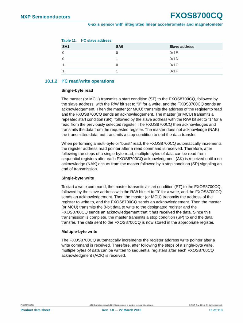
10.1.2 I2C read/write operations
Single-byte read
The master (or MCU) transmits a start condition (ST) to the FXOS8700CQ, followed by the slave address, with the R/W bit set to “0” for a write, and the FXOS8700CQ sends an acknowledgement. Then the master (or MCU) transmits the address of the register to read and the FXOS8700CQ sends an acknowledgement. The master (or MCU) transmits a repeated start condition (SR), followed by the slave address with the R/W bit set to “1” for a read from the previously selected register. The FXOS8700CQ then acknowledges and transmits the data from the requested register. The master does not acknowledge (NAK) the transmitted data, but transmits a stop condition to end the data transfer.Multiple-byte read
When performing a multi-byte or “burst” read, the FXOS8700CQ automatically increments the register address read pointer after a read command is received. Therefore, after following the steps of a single-byte read, multiple bytes of data can be read from sequential registers after each FXOS8700CQ acknowledgment (AK) is received until a no acknowledge (NAK) occurs from the master followed by a stop condition (SP) signaling an end of transmission.
Single-byte write
To start a write command, the master transmits a start condition (ST) to the FXOS8700CQ, followed by the slave address with the R/W bit set to “0” for a write, and the FXOS8700CQ sends an acknowledgement. Then the master (or MCU) transmits the address of the register to write to, and the FXOS8700CQ sends an acknowledgement. Then the master (or MCU) transmits the 8-bit data to write to the designated register and the FXOS8700CQ sends an acknowledgement that it has received the data. Since this transmission is complete, the master transmits a stop condition (SP) to end the data transfer. The data sent to the FXOS8700CQ is now stored in the appropriate register.
Multiple-byte write
The FXOS8700CQ automatically increments the register address write pointer after a write command is received. Therefore, after following the steps of a single-byte write, multiple bytes of data can be written to sequential registers after each FXOS8700CQ acknowledgment (ACK) is received.
Table 11. I2C slave address
SA1 SA0 Slave address
0 0 0x1E
0 1 0x1D
1 0 0x1C
1 1 0x1F
FXOS8700CQ All information provided in this document is subject to legal disclaimers. © NXP B.V. 2016. All rights reserved.
Product data sheet Rev. 7.0 — 22 March 2016 15 of 113
NXP Semiconductors FXOS8700CQ6-axis sensor with integrated linear accelerometer and magnetometer
Fig 6. I2C timing diagram
10.2 SPI interface characteristics
SPI interface is a classical master/slave serial port. The FXOS8700CQ is always considered as the slave and thus is never initiating the communication.
Table 12 and Figure 7 describe the timing requirements for the SPI system.
< Single-byte read >
Master ST Device address[6:0] W Register address[7:0] SR Device address[6:0] R NAK SP
Slave AK AK AK Data[7:0]
< Multiple-byte read >
Master ST Device address[6:0] W Register address[7:0] SR Device address[6:0] R AK
Slave AK AK AK Data[7:0]
Master AK AK NAK SP
Slave Data[7:0] Data[7:0] Data[7:0]
< Multiple-byte write >
Master ST Device address[6:0] W Register address[7:0] Data[7:0] Data[7:0] SP
Slave AK AK AK AK
< Single-byte write >
Master ST Device address[6:0] W Register address[7:0] Data[7:0] SP
Slave AK AK AK
Legend
ST: Start condition SP: Stop condition NAK: No acknowledge W: Write = 0
SR: Repeated start condition AK: Acknowledge R: Read = 1
Table 12. SPI timing
Function Symbol Min Max Unit
Operating frequency Of - 1 MHz
SCLK period tSCLK 1000 - ns
SCLK high time tCLKH 500 - ns
SCLK low time tCLKL 500 - ns
CS_B lead time tSCS 65 - ns
CS_B lag time tHCS 65 - ns
MOSI data setup time tSET 25 - ns
FXOS8700CQ All information provided in this document is subject to legal disclaimers. © NXP B.V. 2016. All rights reserved.
Product data sheet Rev. 7.0 — 22 March 2016 16 of 113
NXP Semiconductors FXOS8700CQ6-axis sensor with integrated linear accelerometer and magnetometer
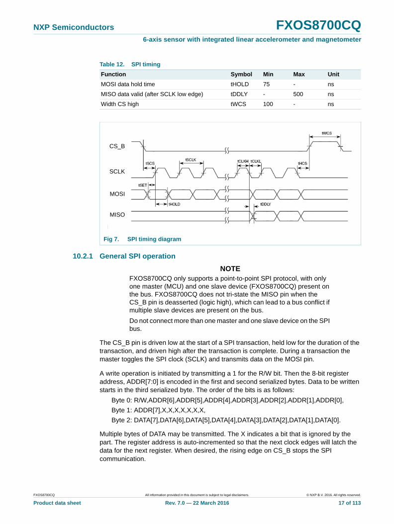
10.2.1 General SPI operation
NOTEFXOS8700CQ only supports a point-to-point SPI protocol, with only one master (MCU) and one slave device (FXOS8700CQ) present on the bus. FXOS8700CQ does not tri-state the MISO pin when the CS_B pin is deasserted (logic high), which can lead to a bus conflict if multiple slave devices are present on the bus.
Do not connect more than one master and one slave device on the SPI bus.
The CS_B pin is driven low at the start of a SPI transaction, held low for the duration of the transaction, and driven high after the transaction is complete. During a transaction the master toggles the SPI clock (SCLK) and transmits data on the MOSI pin.
A write operation is initiated by transmitting a 1 for the R/W bit. Then the 8-bit register address, ADDR[7:0] is encoded in the first and second serialized bytes. Data to be written starts in the third serialized byte. The order of the bits is as follows:
Byte 0: R/W,ADDR[6],ADDR[5],ADDR[4],ADDR[3],ADDR[2],ADDR[1],ADDR[0],
Byte 1: ADDR[7],X,X,X,X,X,X,X,
Byte 2: DATA[7],DATA[6],DATA[5],DATA[4],DATA[3],DATA[2],DATA[1],DATA[0].
Multiple bytes of DATA may be transmitted. The X indicates a bit that is ignored by the part. The register address is auto-incremented so that the next clock edges will latch the data for the next register. When desired, the rising edge on CS_B stops the SPI communication.
MOSI data hold time tHOLD 75 - ns
MISO data valid (after SCLK low edge) tDDLY - 500 ns
Width CS high tWCS 100 - ns
Fig 7. SPI timing diagram
Table 12. SPI timing
Function Symbol Min Max Unit
CS_B
SCLK
MOSI
MISO
FXOS8700CQ All information provided in this document is subject to legal disclaimers. © NXP B.V. 2016. All rights reserved.
Product data sheet Rev. 7.0 — 22 March 2016 17 of 113
NXP Semiconductors FXOS8700CQ6-axis sensor with integrated linear accelerometer and magnetometer
The FXOS8700CQ SPI configuration is as follows:
• Polarity: rising/falling
• Phase: sample/setup
• Order: MSB first
Data is sampled during the rising edge of SCLK and set up during the falling edge of SCLK.
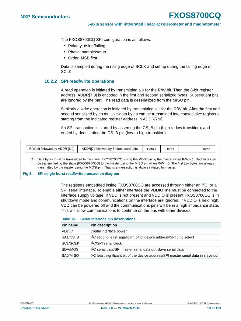
10.2.2 SPI read/write operations
A read operation is initiated by transmitting a 0 for the R/W bit. Then the 8-bit register address, ADDR[7:0] is encoded in the first and second serialized bytes. Subsequent bits are ignored by the part. The read data is deserialized from the MISO pin.
Similarly a write operation is initiated by transmitting a 1 for the R/W bit. After the first and second serialized bytes multiple-data bytes can be transmitted into consecutive registers, starting from the indicated register address in ADDR[7:0].
An SPI transaction is started by asserting the CS_B pin (high-to-low transition), and ended by deasserting the CS_B pin (low-to-high transition).
The registers embedded inside FXOS8700CQ are accessed through either an I2C, or a SPI serial interface. To enable either interface the VDDIO line must be connected to the interface supply voltage. If VDD is not present and VDDIO is present FXOS8700CQ is in shutdown mode and communications on the interface are ignored. If VDDIO is held high, VDD can be powered off and the communications pins will be in a high impedance state. This will allow communications to continue on the bus with other devices.
(1) Data bytes must be transmitted to the slave (FXOS8700CQ) using the MOSI pin by the master when R/W = 1. Data bytes will be transmitted by the slave (FXOS8700CQ) to the master using the MISO pin when R/W = 0. The first two bytes are always transmitted by the master using the MOSI pin. That is, a transaction is always initiated by master.
Fig 8. SPI single-burst read/write transaction diagram
Table 13. Serial interface pin descriptions
Pin name Pin description
VDDIO Digital interface power
SA1/CS_B I2C second least significant bit of device address/SPI chip select
SCL/SCLK I2C/SPI serial clock
SDA/MOSI I2C serial data/SPI master serial data out slave serial data in
SA0/MISO I2C least significant bit of the device address/SPI master serial data in slave out
FXOS8700CQ All information provided in this document is subject to legal disclaimers. © NXP B.V. 2016. All rights reserved.
Product data sheet Rev. 7.0 — 22 March 2016 18 of 113
NXP Semiconductors FXOS8700CQ6-axis sensor with integrated linear accelerometer and magnetometer
10.2.3 I2C/SPI auto detection
FXOS8700CQ employs an interface mode, auto-detection circuit that will select either I2C or SPI interface mode based on the state of the SA0 pin during power up or when exiting reset. Once set for I2C or SPI operation, the device will remain in I2C or SPI mode until the device is reset or powered down and the auto-detection process is repeated. Please note that when SPI interface mode is desired, care must be taken to ensure that no other slave device drives the common SA0/MISO pin during the 1 ms period after a hard or soft reset or powerup event.
10.2.4 Power supply sequencing and I2C/SPI mode auto-detection
FXOS8700CQ does not have any specific power supply sequencing requirements between VDD and VDDIO voltage supplies to ensure normal operation. To ensure correct operation of the I2C/SPI auto-detection function, VDDIO should be applied before or at the same time as VDD. If this order cannot be maintained, the user should either toggle the RST line or power cycle the VDD rail in order to force the auto-detect function to restart and correctly identify the desired interface. FXOS8700CQ will indicate completion of the reset sequence by toggling the INT1 pin from logic high to low to high over a 500 ns period. If the INT1 pin was already low prior to the reset event, it will only go high.
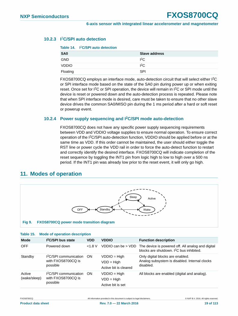
11. Modes of operation
Table 14. I2C/SPI auto detection
SA0 Slave address
GND I2C
VDDIO I2C
Floating SPI
Fig 9. FXOS8700CQ power mode transition diagram
Table 15. Mode of operation description
Mode I2C/SPI bus state VDD VDDIO Function description
OFF Powered down <1.8 V VDDIO can be > VDD The device is powered off. All analog and digital blocks are shutdown. I2C bus inhibited.
Standby I2C/SPI communication with FXOS8700CQ is possible
ON VDDIO = High
VDD = High
Active bit is cleared
Only digital blocks are enabled. Analog subsystem is disabled. Internal clocks disabled.
Active(wake/sleep)
I2C/SPI communication with FXOS8700CQ is possible
ON VDDIO = High
VDD = High
Active bit is set
All blocks are enabled (digital and analog).
FXOS8700CQ All information provided in this document is subject to legal disclaimers. © NXP B.V. 2016. All rights reserved.
Product data sheet Rev. 7.0 — 22 March 2016 19 of 113
NXP Semiconductors FXOS8700CQ6-axis sensor with integrated linear accelerometer and magnetometer
All register contents are preserved when transitioning from active-to-standby mode, but some registers are reset when transitioning from standby-to-active. These registers are noted in Table16. The sleep and wake modes are active modes. For more information on how to use the sleep and wake modes and configuring the device to transition between them, please refer to Section 12 or NXP application note AN4074.
12. Embedded functionality
FXOS8700CQ is a low-power, digital output, 6-axis sensor with both I2C and SPI interfaces. Extensive embedded functionality is provided to detect inertial and magnetic events at low power, with the ability to notify the host processor of an event using either of the two programmable interrupt pins. The embedded functionality includes:
• 8-bit or 14-bit accelerometer data which includes high-pass filtered data, and 8-bit or 16-bit magnetometer data
• Four different oversampling options for the accelerometer output data, and eight for the magnetometer. The oversampling settings allow the end user to optimize the resolution versus power trade-off in a given application.
• A low-noise accelerometer mode that functions independently of the oversampling modes for even higher resolution
• Low-power, auto-wake/sleep function for conserving power in portable battery powered applications
• Accelerometer pulse-detection circuit which can be used to detect directional single and double taps
• Accelerometer directional motion- and freefall-event detection with programmable threshold and debounce time
• Acceleration transient detection with programmable threshold and debounce time. Transient detection can employ either a high-pass filter or use the difference between reference and current sample values.
• Orientation detection with programmable hysteresis for smooth transitions between portrait/landscape orientations
• Accelerometer vector-magnitude change event detection with programmable reference, threshold, and debounce time values
• Magnetic threshold event detection with programmable reference, threshold, and debounce time
• Magnetometer vector-magnitude change event detection with programmable reference, threshold and debounce time values
• Magnetic min/max detection circuit which can also be used for autonomous calibration of magnetic hard-iron offset
Many different configurations of the above functions are possible to suit the needs of the end application. Separate application notes are available to further explain the different configuration settings and potential use cases.
12.1 Factory calibration
FXOS8700CQ's integrated accelerometer and magnetometer sensors are factory calibrated for sensitivity and offset on each axis. The trim values are stored in non-volatile memory (NVM). On power-up, the trim parameters are read from NVM and applied to the internal compensation circuitry. After mounting the device to the PCB, the user may
FXOS8700CQ All information provided in this document is subject to legal disclaimers. © NXP B.V. 2016. All rights reserved.
Product data sheet Rev. 7.0 — 22 March 2016 20 of 113
NXP Semiconductors FXOS8700CQ6-axis sensor with integrated linear accelerometer and magnetometer
further adjust the accelerometer and magnetometer offsets through the OFF_X/Y/Z and M_OFF_X/Y/Z registers, respectively. For more information on device calibration, refer to NXP application note, AN4399.
12.2 8-bit or 14-bit accelerometer data
The measured acceleration data is stored in the OUT_X_MSB, OUT_X_LSB, OUT_Y_MSB, OUT_Y_LSB, OUT_Z_MSB, and OUT_Z_LSB registers as 2’s complement 14-bit numbers. The most significant 8-bits of each axis are stored in the OUT_X/Y/Z_MSB registers, so applications needing only 8-bit results simply read these three registers and ignore the OUT_X/Y/Z_LSB registers. To do this, the f_read mode bit in CTRL_REG1 must be set.
When the full-scale range is set to 2 g, the measurement range is –2 g to +1.999 g, and each count corresponds to 0.244 mg at ±14-bits resolution. When the full-scale is set to 8 g, the measurement range is –8 g to +7.996 g, and each count corresponds to 0.976 mg. The resolution is reduced by a factor of 64 if only the 8-bit results are used (CTRL_REG1[f_read] = 1). For further information on the different data formats and modes, please refer to NXP application note AN4076.
12.3 Accelerometer low-power modes versus high-resolution modes
FXOS8700CQ can be optimized for lower power or higher resolution of the accelerometer output data. High resolution is achieved by setting the lnoise bit in register 0x2A. This improves the resolution (by lowering the noise), but be aware that the full-scale range setting is restricted to ±2 g or ±4 g when this bit is set. This will affect all internal embedded functions (scaling of thresholds, etc.) and reduce noise. Another method for improving the resolution of the data is through oversampling. One of the oversampling schemes of the output data can be activated when CTRL_REG2[mods] = 0b10 which will improve the resolution of the output data without affecting the internal embedded functions or fixing the dynamic range.
There is a trade-off between low power and high resolution. Low power can be achieved when the oversampling rate is reduced. When CTRL_REG2[mods] = 0b10, the lowest power is achieved, at the expense of higher noise. In general, the lower the selected ODR and OSR, the lower the power consumption. For more information on how to configure the device in low-power or high-resolution modes and understand the benefits and trade-offs, please refer to NXP application note AN4075.
12.4 Auto-wake/sleep mode
FXOS8700CQ can be configured to transition between sample rates (with their respective current consumptions) based on the status of the embedded interrupt event generators in the device. The advantage of using the auto-wake/sleep is that the system can automatically transition to a higher sample rate (higher current consumption) when needed but spends the majority of the time in the sleep mode (lower current) when the device does not require higher sampling rates. Auto-wake refers to the device being triggered by one of the interrupt event functions to transition to a higher sample rate. This may also interrupt the processor to transition from a sleep mode to a higher power mode.
FXOS8700CQ All information provided in this document is subject to legal disclaimers. © NXP B.V. 2016. All rights reserved.
Product data sheet Rev. 7.0 — 22 March 2016 21 of 113
NXP Semiconductors FXOS8700CQ6-axis sensor with integrated linear accelerometer and magnetometer
Sleep mode occurs when none of the enabled interrupt event functions has detected an interrupt within the user-defined, time-out period. The device will then transition to the specified lower sample rate. It may also alert the processor to go into a lower power mode to save power during this period of inactivity. Refer to AN4074 for more detailed information on configuring the auto-wake/sleep function.
12.5 Hybrid mode
FXOS8700CQ uses a single common analog-to-digital converter (ADC) for both the accelerometer and magnetometer. When operating in hybrid mode (M_CTRL_REG1[m_hms] = 0b11), both the accelerometer and magnetometer sensors are actively measured by the ADC at an ODR equal to one half of the setting made in CTRL_REG1[dr] when operating in accelerometer-only mode (M_CTRL_REG1[m_hms] = 0b00 (default)) or magnetometer-only mode (M_CTRL_REG1[m_hms] = 0b01). While the ODR is common to both sensors when operating in hybrid mode, the OSR settings for each sensor are independent and may be set using the CTRL_REG2[mods] for the accelerometer and M_CTRL_REG1[m_os] for the magnetometer, respectively.
12.6 Accelerometer freefall and motion event detection
FXOS8700CQ integrates a programmable threshold based acceleration detection function capable of detecting either motion or freefall events depending upon the configuration. For further details and examples on using the embedded freefall and motion detection functions, refer to NXP application note AN4070.
12.6.1 Freefall detection
The detection of “Freefall” involves the monitoring of the X, Y, and Z axes for the condition where the acceleration magnitude is below a user-specified threshold for a user-definable amount of time. Typically, the usable threshold ranges are between ±100 mg and ±500 mg.
12.6.2 Motion detection
Motion detection is often used to alert the main processor that the device is currently in use. When the acceleration exceeds a set threshold for a set amount of time, the motion interrupt is asserted. A motion can be a fast moving shake or a slow moving tilt. This will depend on the threshold and timing values configured for the event. The motion detection function can analyze static acceleration changes or faster jolts. The timing value is set by a configurable debounce counter. The debounce counter acts like a filter to indicate whether the condition exists for longer than a set amount of time (that is, 100 ms or longer). There is also directional data available in the source register to detect the direction of the motion that generated the interrupt. This is useful for applications such as directional shake or flick detection, and can also assist gesture detection algorithms by indicating that a motion gesture has started.
12.7 Transient detection
FXOS8700CQ integrates an acceleration transient detection function that incorporates a high-pass filter. Acceleration data goes through the high-pass filter, eliminating the DC tilt offset and low frequency acceleration changes. The high-pass filter cutoff can be set by the user to four different frequencies which are dependent on the selected output data
FXOS8700CQ All information provided in this document is subject to legal disclaimers. © NXP B.V. 2016. All rights reserved.
Product data sheet Rev. 7.0 — 22 March 2016 22 of 113
NXP Semiconductors FXOS8700CQ6-axis sensor with integrated linear accelerometer and magnetometer
rate (ODR). A higher cutoff frequency ensures that DC and slowly changing acceleration data will be filtered out, allowing only the higher frequencies to pass. The transient detection feature can be used in the same manner as the motion detection by bypassing the high-pass filter. There is an option in the configuration register to do this. This adds more flexibility to cover the various customer use cases.
Many applications use the accelerometer’s static acceleration readings (that is, tilt) which measure the change in acceleration due to gravity only. These functions benefit from acceleration data being filtered with a low-pass filter where high-frequency data is considered noise. However, there are many functions where the accelerometer must analyze dynamic acceleration. Functions such as tap, flick, shake and step counting are based on the analysis of the change in the dynamic acceleration. The transient detection function can be routed to either interrupt pin through bit 5 in CTRL_REG5 register (0x2E). Registers 0x1D – 0x20 are used for configuring the transient detection function. The source register contains directional data to determine the direction of the transient acceleration, either positive or negative. For further information of the embedded transient detection function along with specific application examples and recommended configuration settings, refer to NXP application note AN4461.
12.8 Pulse detection
FXOS8700CQ has embedded single/double and directional pulse detection. This function employs several timers for programming the pulse width time and the latency between pulses. The detection thresholds are independently programmable for each axis. The acceleration data input to the pulse detection circuit can be put through both high and low-pass filters, allowing for greater flexibility in discriminating between pulse and tap events. The PULSE_SRC register provides information on the axis, direction (polarity), and single/double event status for the detected pulse or tap. For more information on how to configure the device for pulse detection, please refer to NXP application note AN4072.
12.9 Orientation detection
FXOS8700CQ has an embedded orientation detection algorithm with the ability to detect all six orientations. The transition angles and hysteresis are programmable, allowing for a smooth transition between portrait and landscape orientations.
The angle at which the device no longer detects the orientation change is referred to as the “Z-lockout angle”. The device operates down to 29° from the flat position. All angles are accurate to ±2°.
For further information on the orientation detection function refer to NXP application note, AN4068.
12.10 Acceleration vector-magnitude detection
FXOS8700CQ incorporates an acceleration vector-magnitude change detection block that can be configured to generate an interrupt when the acceleration magnitude exceeds a preset threshold for a programmed debounce time. The function can be configured to operate in absolute or relative modes, and can also act as a wake-to-sleep/sleep-to-wake source. This function is useful for detecting acceleration transients when operated in absolute mode, or for detecting changes in orientation when operated in relative mode, refer to NXP application note AN4692.
FXOS8700CQ All information provided in this document is subject to legal disclaimers. © NXP B.V. 2016. All rights reserved.
Product data sheet Rev. 7.0 — 22 March 2016 23 of 113
NXP Semiconductors FXOS8700CQ6-axis sensor with integrated linear accelerometer and magnetometer
12.11 Magnetic vector-magnitude detection
FXOS8700CQ incorporates a magnetic vector-magnitude change detection block that can be configured to generate an interrupt when the magnetic field magnitude exceeds a preset threshold for a programmed debounce time. The function can be configured to operate in absolute or relative modes, and can also act as a wake-to-sleep/sleep-to-wake source. For more information, refer to NXP application note AN4458.
12.12 Magnetic threshold detection
FXOS8700CQ incorporates a magnetic threshold event detection block that can be configured to generate an interrupt when the magnetic field on the enabled axes is above or below a programmed threshold.
Two logic combinations are possible for the detection: all of the enabled axes below their respective thresholds (AND condition), or any of the enabled axes above their respective thresholds (OR condition). Even detection may be filtered using a dedicated debounce counter to avoid spurious event detection. The thresholds for each axis are individually programmable and the function can also act as a wake-to-sleep/sleep-to-wake source.
12.13 Magnetic min/max detection (autonomous calibration)
FXOS8700CQ incorporates a magnetic min/max detection circuit that can be used to automatically track the minimum and maximum field values measured on each of the X, Y, and Z axes. The stored minimum and maximum values may optionally be used to determine the magnetic hard-iron compensation and load the offset registers with the appropriate correction values. For more information, refer to NXP application note AN4459.
FXOS8700CQ All information provided in this document is subject to legal disclaimers. © NXP B.V. 2016. All rights reserved.
Product data sheet Rev. 7.0 — 22 March 2016 24 of 113
NXP Semiconductors FXOS8700CQ6-axis sensor with integrated linear accelerometer and magnetometer
13. Example FXOS8700CQ driver code
13.1 Introduction
It is very straightforward to configure the FXOS8700CQ and start receiving data from the three accelerometer and three magnetometer channels. Unfortunately, since every hardware platform will be different, it is not possible to provide completely portable software drivers. This section therefore provides real FXOS8700CQ driver code for a Kinetis uC board running under the MQX operating system. The I2C functions s_i2c_read_regs and s_i2c_write_regs are not provided here and should be replaced with the corresponding low level I2C driver code on the development platform.
13.2 FXOS8700CQ addresses
This section lists the I2C address of the FXOS8700CQ. The I2C address depends on the logic level of FXOS8700CQ’s SA0 and SA1 address selection pins, so the actual I2C address may be 0x1C, 0x1D, 0x1E or 0x1F.
Please see Table 11, “I2C slave address,” on page 15 for the available I2C addresses and SA1/SA0 settings.
Example 1. // FXOS8700CQ I2C address#define FXOS8700CQ_SLAVE_ADDR 0x1E // with pins SA0=0, SA1=0
Some of the key FXOS8700CQ internal register addresses are listed below.
Example 2. // FXOS8700CQ internal register addresses#define FXOS8700CQ_STATUS 0x00#define FXOS8700CQ_WHOAMI 0x0D#define FXOS8700CQ_XYZ_DATA_CFG 0x0E#define FXOS8700CQ_CTRL_REG1 0x2A#define FXOS8700CQ_M_CTRL_REG1 0x5B#define FXOS8700CQ_M_CTRL_REG2 0x5C#define FXOS8700CQ_WHOAMI_VAL 0xC7
The reference driver code shown in this example does a block read of the FXOS8700CQ status byte and three 16-bit accelerometer channels plus three 16-bit magnetometer channels for a total of 13 bytes in a single I2C read operation.
Example 3. // number of bytes to be read from the FXOS8700CQ#define FXOS8700CQ_READ_LEN 13 // status plus 6 channels = 13 bytes
FXOS8700CQ All information provided in this document is subject to legal disclaimers. © NXP B.V. 2016. All rights reserved.
Product data sheet Rev. 7.0 — 22 March 2016 25 of 113
NXP Semiconductors FXOS8700CQ6-axis sensor with integrated linear accelerometer and magnetometer
13.3 Sensor data structure
The high and low bytes of the three accelerometer and three magnetometer channels are placed into a structure of type SRAWDATA containing three signed short integers.
Example 4. typedef struct{
int16_t x;int16_t y;int16_t z;
} SRAWDATA;
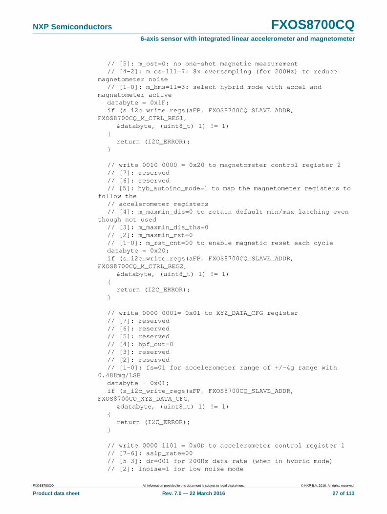
13.4 FXOS8700CQ configuration function
This function configures the FXOS8700CQ for 200-Hz hybrid mode meaning that both accelerometer and magnetometer data are provided at the 200-Hz rate. The code is self-explanatory and can be easily customized for different settings.
Example 5. // function configures FXOS8700CQ combination accelerometer and magnetometer sensor static _mqx_ints_FXOS8700CQ_start(MQX_FILE_PTR aFP){
uint8_t databyte;
// read and check the FXOS8700CQ WHOAMI registerif (s_i2c_read_regs(aFP, FXOS8700CQ_SLAVE_ADDR,
FXOS8700CQ_WHOAMI, &databyte,(uint8_t) 1) != 1)
{return (I2C_ERROR);
}if (databyte != FXOS8700CQ_WHOAMI_VAL){
return (I2C_ERROR);}
// write 0000 0000 = 0x00 to accelerometer control register 1 to place FXOS8700CQ into
// standby// [7-1] = 0000 000// [0]: active=0databyte = 0x00;if (s_i2c_write_regs(aFP, FXOS8700CQ_SLAVE_ADDR,
FXOS8700CQ_CTRL_REG1, &databyte, (uint8_t) 1) != 1)
{return (I2C_ERROR);
}
// write 0001 1111 = 0x1F to magnetometer control register 1// [7]: m_acal=0: auto calibration disabled// [6]: m_rst=0: no one-shot magnetic reset
FXOS8700CQ All information provided in this document is subject to legal disclaimers. © NXP B.V. 2016. All rights reserved.
Product data sheet Rev. 7.0 — 22 March 2016 26 of 113
NXP Semiconductors FXOS8700CQ6-axis sensor with integrated linear accelerometer and magnetometer
// [5]: m_ost=0: no one-shot magnetic measurement// [4-2]: m_os=111=7: 8x oversampling (for 200Hz) to reduce
magnetometer noise// [1-0]: m_hms=11=3: select hybrid mode with accel and
magnetometer activedatabyte = 0x1F;if (s_i2c_write_regs(aFP, FXOS8700CQ_SLAVE_ADDR,
FXOS8700CQ_M_CTRL_REG1, &databyte, (uint8_t) 1) != 1)
{return (I2C_ERROR);
}
// write 0010 0000 = 0x20 to magnetometer control register 2// [7]: reserved// [6]: reserved// [5]: hyb_autoinc_mode=1 to map the magnetometer registers to
follow the // accelerometer registers// [4]: m_maxmin_dis=0 to retain default min/max latching even
though not used// [3]: m_maxmin_dis_ths=0// [2]: m_maxmin_rst=0// [1-0]: m_rst_cnt=00 to enable magnetic reset each cycledatabyte = 0x20;if (s_i2c_write_regs(aFP, FXOS8700CQ_SLAVE_ADDR,
FXOS8700CQ_M_CTRL_REG2, &databyte, (uint8_t) 1) != 1)
{return (I2C_ERROR);
}
// write 0000 0001= 0x01 to XYZ_DATA_CFG register// [7]: reserved// [6]: reserved// [5]: reserved// [4]: hpf_out=0// [3]: reserved// [2]: reserved// [1-0]: fs=01 for accelerometer range of +/-4g range with
0.488mg/LSBdatabyte = 0x01;if (s_i2c_write_regs(aFP, FXOS8700CQ_SLAVE_ADDR,
FXOS8700CQ_XYZ_DATA_CFG, &databyte, (uint8_t) 1) != 1)
{return (I2C_ERROR);
}
// write 0000 1101 = 0x0D to accelerometer control register 1// [7-6]: aslp_rate=00// [5-3]: dr=001 for 200Hz data rate (when in hybrid mode)// [2]: lnoise=1 for low noise mode
FXOS8700CQ All information provided in this document is subject to legal disclaimers. © NXP B.V. 2016. All rights reserved.
Product data sheet Rev. 7.0 — 22 March 2016 27 of 113
NXP Semiconductors FXOS8700CQ6-axis sensor with integrated linear accelerometer and magnetometer
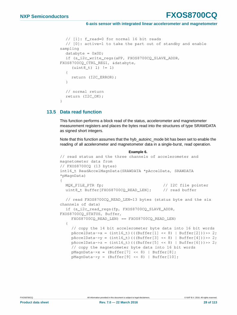
// [1]: f_read=0 for normal 16 bit reads// [0]: active=1 to take the part out of standby and enable
samplingdatabyte = 0x0D; if (s_i2c_write_regs(aFP, FXOS8700CQ_SLAVE_ADDR,
FXOS8700CQ_CTRL_REG1, &databyte, (uint8_t) 1) != 1)
{return (I2C_ERROR);
}
// normal returnreturn (I2C_OK);
}
13.5 Data read function
This function performs a block read of the status, accelerometer and magnetometer measurement registers and places the bytes read into the structures of type SRAWDATA as signed short integers.
Note that this function assumes that the hyb_autoinc_mode bit has been set to enable the reading of all accelerometer and magnetometer data in a single-burst, read operation.
Example 6. // read status and the three channels of accelerometer and magnetometer data from // FXOS8700CQ (13 bytes)int16_t ReadAccelMagnData(SRAWDATA *pAccelData, SRAWDATA *pMagnData){
MQX_FILE_PTR fp; // I2C file pointeruint8_t Buffer[FXOS8700CQ_READ_LEN]; // read buffer
// read FXOS8700CQ_READ_LEN=13 bytes (status byte and the six channels of data)
if (s_i2c_read_regs(fp, FXOS8700CQ_SLAVE_ADDR, FXOS8700CQ_STATUS, Buffer,
FXOS8700CQ_READ_LEN) == FXOS8700CQ_READ_LEN){
// copy the 14 bit accelerometer byte data into 16 bit wordspAccelData->x = (int16_t)(((Buffer[1] << 8) | Buffer[2]))>> 2;pAccelData->y = (int16_t)(((Buffer[3] << 8) | Buffer[4]))>> 2;pAccelData->z = (int16_t)(((Buffer[5] << 8) | Buffer[6]))>> 2;// copy the magnetometer byte data into 16 bit wordspMagnData->x = (Buffer[7] << 8) | Buffer[8];pMagnData->y = (Buffer[9] << 8) | Buffer[10];
FXOS8700CQ All information provided in this document is subject to legal disclaimers. © NXP B.V. 2016. All rights reserved.
Product data sheet Rev. 7.0 — 22 March 2016 28 of 113
NXP Semiconductors FXOS8700CQ6-axis sensor with integrated linear accelerometer and magnetometer
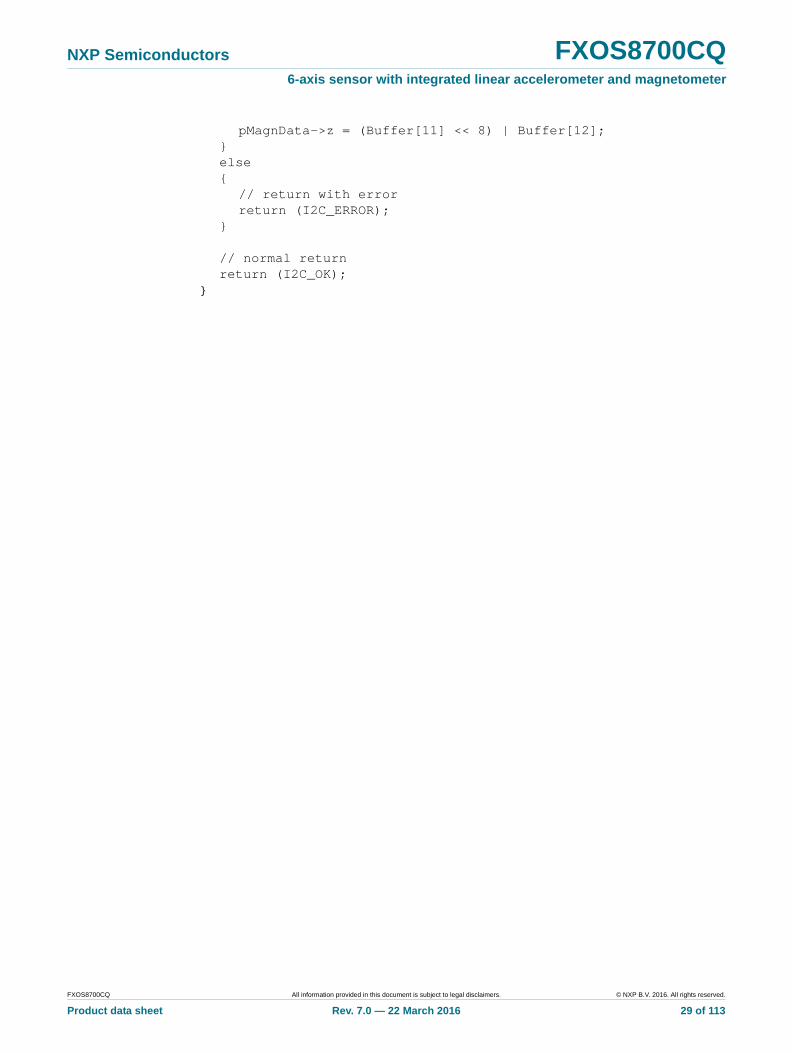
pMagnData->z = (Buffer[11] << 8) | Buffer[12];}else{
// return with errorreturn (I2C_ERROR);
}
// normal returnreturn (I2C_OK);
}
FXOS8700CQ All information provided in this document is subject to legal disclaimers. © NXP B.V. 2016. All rights reserved.
Product data sheet Rev. 7.0 — 22 March 2016 29 of 113
NXP Semiconductors FXOS8700CQ6-axis sensor with integrated linear accelerometer and magnetometer
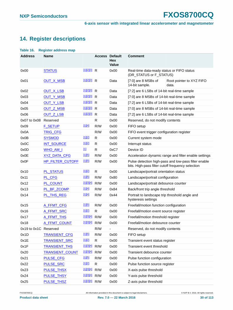
14. Register descriptions
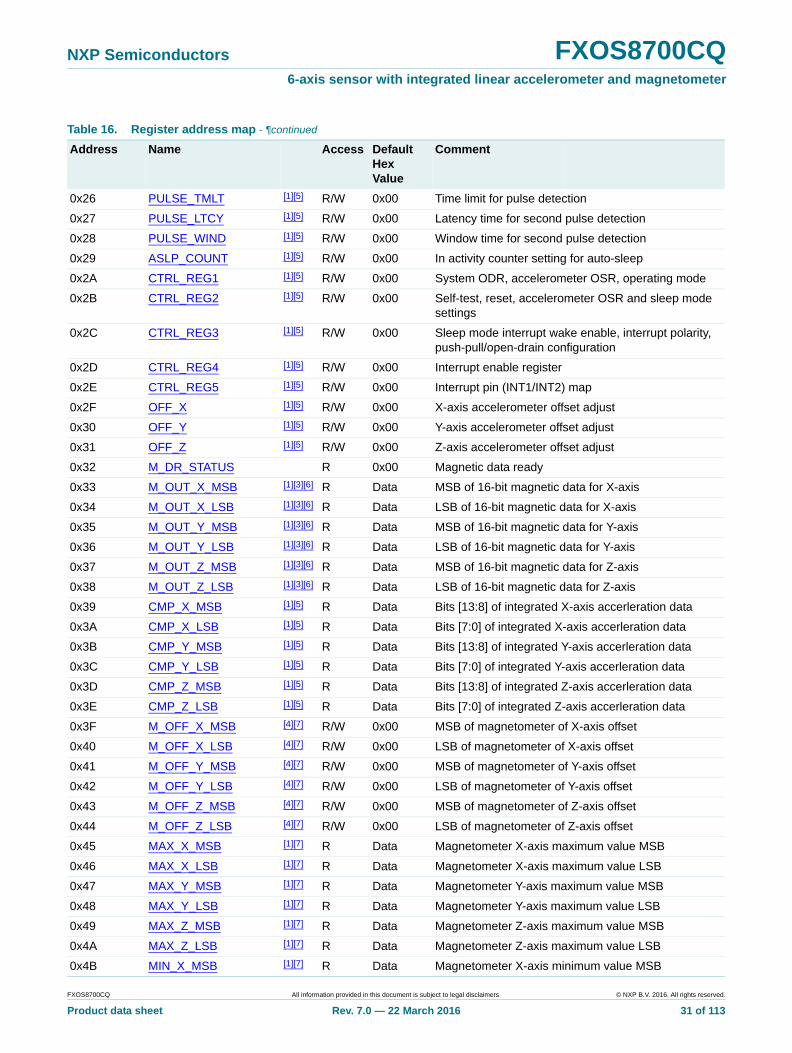
Table 16. Register address map
Address Name Access DefaultHexValue
Comment
0x00 STATUS [1][2][3] R 0x00 Real-time data-ready status or FIFO status (DR_STATUS or F_STATUS)
0x01 OUT_X_MSB [1][2][3] R Data [7:0] are 8 MSBs of 14-bit sample.
Root pointer to XYZ FIFO data.
0x02 OUT_X_LSB [1][2][3] R Data [7:2] are 6 LSBs of 14-bit real-time sample
0x03 OUT_Y_MSB [1][2][3] R Data [7:0] are 8 MSBs of 14-bit real-time sample
0x04 OUT_Y_LSB [1][2][3] R Data [7:2] are 6 LSBs of 14-bit real-time sample
0x05 OUT_Z_MSB [1][2][3] R Data [7:0] are 8 MSBs of 14-bit real-time sample
0x06 OUT_Z_LSB [1][2][3] R Data [7:2] are 6 LSBs of 14-bit real-time sample
0x07 to 0x08 Reserved R 0x00 Reserved, do not modify contents
0x09 F_SETUP [1][4] R/W 0x00 FIFO setup
0x0A TRIG_CFG R/W 0x00 FIFO event trigger configuration register
0x0B SYSMOD [1][2] R 0x00 Current system mode
0x0C INT_SOURCE [1][2] R 0x00 Interrupt status
0x0D WHO_AM_I [1] R 0xC7 Device ID
0x0E XYZ_DATA_CFG [1][5] R/W 0x00 Acceleration dynamic range and filter enable settings
0x0F HP_FILTER_CUTOFF [1][5] R/W 0x00 Pulse detection high-pass and low-pass filter enable bits. High-pass filter cutoff frequency selection
0x10 PL_STATUS [1][2] R 0x00 Landscape/portrait orientation status
0x11 PL_CFG [1][5] R/W 0x80 Landscape/portrait configuration
0x12 PL_COUNT [1][3][4] R/W 0x00 Landscape/portrait debounce counter
0x13 PL_BF_ZCOMP [1][4] R/W 0x84 Back/front trip angle threshold
0x14 PL_THS_REG [1][4] R/W 0x44 Portrait to landscape trip threshold angle and hysteresis settings
0x15 A_FFMT_CFG [1][5] R/W 0x00 Freefall/motion function configuration
0x16 A_FFMT_SRC [1][2] R 0x00 Freefall/motion event source register
0x17 A_FFMT_THS [1][3][4] R/W 0x00 Freefall/motion threshold register
0x18 A_FFMT_COUNT [1][3][4] R/W 0x00 Freefall/motion debounce counter
0x19 to 0x1C Reserved R/W - Reserved, do not modify contents
0x1D TRANSIENT_CFG [1][5] R/W 0x00 FIFO setup
0x1E TRANSIENT_SRC [1][2] R 0x00 Transient event status register
0x1F TRANSIENT_THS [1][3][4] R/W 0x00 Transient event threshold
0x20 TRANSIENT_COUNT [1][3][4] R/W 0x00 Transient debounce counter
0x21 PULSE_CFG [1][5] R/W 0x00 Pulse function configuration
0x22 PULSE_SRC [1][2] R 0x00 Pulse function source register
0x23 PULSE_THSX [1][3][4] R/W 0x00 X-axis pulse threshold
0x24 PULSE_THSY [1][3][4] R/W 0x00 Y-axis pulse threshold
0x25 PULSE_THSZ [1][3][4] R/W 0x00 Z-axis pulse threshold
FXOS8700CQ All information provided in this document is subject to legal disclaimers. © NXP B.V. 2016. All rights reserved.
Product data sheet Rev. 7.0 — 22 March 2016 30 of 113
NXP Semiconductors FXOS8700CQ6-axis sensor with integrated linear accelerometer and magnetometer
0x26 PULSE_TMLT [1][5] R/W 0x00 Time limit for pulse detection
0x27 PULSE_LTCY [1][5] R/W 0x00 Latency time for second pulse detection
0x28 PULSE_WIND [1][5] R/W 0x00 Window time for second pulse detection
0x29 ASLP_COUNT [1][5] R/W 0x00 In activity counter setting for auto-sleep
0x2A CTRL_REG1 [1][5] R/W 0x00 System ODR, accelerometer OSR, operating mode
0x2B CTRL_REG2 [1][5] R/W 0x00 Self-test, reset, accelerometer OSR and sleep mode settings
0x2C CTRL_REG3 [1][5] R/W 0x00 Sleep mode interrupt wake enable, interrupt polarity, push-pull/open-drain configuration
0x2D CTRL_REG4 [1][5] R/W 0x00 Interrupt enable register
0x2E CTRL_REG5 [1][5] R/W 0x00 Interrupt pin (INT1/INT2) map
0x2F OFF_X [1][5] R/W 0x00 X-axis accelerometer offset adjust
0x30 OFF_Y [1][5] R/W 0x00 Y-axis accelerometer offset adjust
0x31 OFF_Z [1][5] R/W 0x00 Z-axis accelerometer offset adjust
0x32 M_DR_STATUS R 0x00 Magnetic data ready
0x33 M_OUT_X_MSB [1][3][6] R Data MSB of 16-bit magnetic data for X-axis
0x34 M_OUT_X_LSB [1][3][6] R Data LSB of 16-bit magnetic data for X-axis
0x35 M_OUT_Y_MSB [1][3][6] R Data MSB of 16-bit magnetic data for Y-axis
0x36 M_OUT_Y_LSB [1][3][6] R Data LSB of 16-bit magnetic data for Y-axis
0x37 M_OUT_Z_MSB [1][3][6] R Data MSB of 16-bit magnetic data for Z-axis
0x38 M_OUT_Z_LSB [1][3][6] R Data LSB of 16-bit magnetic data for Z-axis
0x39 CMP_X_MSB [1][5] R Data Bits [13:8] of integrated X-axis accerleration data
0x3A CMP_X_LSB [1][5] R Data Bits [7:0] of integrated X-axis accerleration data
0x3B CMP_Y_MSB [1][5] R Data Bits [13:8] of integrated Y-axis accerleration data
0x3C CMP_Y_LSB [1][5] R Data Bits [7:0] of integrated Y-axis accerleration data
0x3D CMP_Z_MSB [1][5] R Data Bits [13:8] of integrated Z-axis accerleration data
0x3E CMP_Z_LSB [1][5] R Data Bits [7:0] of integrated Z-axis accerleration data
0x3F M_OFF_X_MSB [4][7] R/W 0x00 MSB of magnetometer of X-axis offset
0x40 M_OFF_X_LSB [4][7] R/W 0x00 LSB of magnetometer of X-axis offset
0x41 M_OFF_Y_MSB [4][7] R/W 0x00 MSB of magnetometer of Y-axis offset
0x42 M_OFF_Y_LSB [4][7] R/W 0x00 LSB of magnetometer of Y-axis offset
0x43 M_OFF_Z_MSB [4][7] R/W 0x00 MSB of magnetometer of Z-axis offset
0x44 M_OFF_Z_LSB [4][7] R/W 0x00 LSB of magnetometer of Z-axis offset
0x45 MAX_X_MSB [1][7] R Data Magnetometer X-axis maximum value MSB
0x46 MAX_X_LSB [1][7] R Data Magnetometer X-axis maximum value LSB
0x47 MAX_Y_MSB [1][7] R Data Magnetometer Y-axis maximum value MSB
0x48 MAX_Y_LSB [1][7] R Data Magnetometer Y-axis maximum value LSB
0x49 MAX_Z_MSB [1][7] R Data Magnetometer Z-axis maximum value MSB
0x4A MAX_Z_LSB [1][7] R Data Magnetometer Z-axis maximum value LSB
0x4B MIN_X_MSB [1][7] R Data Magnetometer X-axis minimum value MSB
Table 16. Register address map - ¶continued
Address Name Access DefaultHexValue
Comment
FXOS8700CQ All information provided in this document is subject to legal disclaimers. © NXP B.V. 2016. All rights reserved.
Product data sheet Rev. 7.0 — 22 March 2016 31 of 113
NXP Semiconductors FXOS8700CQ6-axis sensor with integrated linear accelerometer and magnetometer
0x4C MIN_X_LSB [1][7] R Data Magnetometer X-axis minimum value LSB
0x4D MIN_Y_MSB [1][7] R Data Magnetometer Y-axis minimum value MSB
0x4E MIN_Y_LSB [1][7] R Data Magnetometer Y-axis minimum value LSB
0x4F MIN_Z_MSB [1][7] R Data Magnetometer Z-axis minimum value MSB
0x50 MIN_Z_LSB [1][7] R Data Magnetometer Z-axis minimum value LSB
0x51 TEMP [1] R Data Device temperature, valid range of –128 to 127 °C when M_CTRL1[m_hms] > 0b00
0x52 M_THS_CFG [1][5] R/W 0x00 Magnetic threshold detection function configuration
0x53 M_THS_SRC [1][2] R Data Magnetic threshold event source register
0x54 M_THS_X_MSB [1][5] R/W 0x00 X-axis magnetic threshold MSB
0x55 M_THS_X_LSB [1][5] R/W 0x00 X-axis magnetic threshold LSB
0x56 M_THS_Y_MSB [1][5] R/W 0x00 Y-axis magnetic threshold MSB
0x57 M_THS_Y_LSB [1][5] R/W 0x00 Y-axis magnetic threshold LSB
0x58 M_THS_Z_MSB [1][5] R/W 0x00 Z-axis magnetic threshold MSB
0x59 M_THS_Z_LSB [1][5] R/W 0x00 Z-axis magnetic threshold LSB
0x5A M_THS_COUNT [1][3][5] R/W 0x00 Magnetic threshold debounce counter
0x5B M_CTRL_REG1 [4] R/W 0x00 Control for magnetic sensor functions
0x5C M_CTRL_REG2 [5] R/W 0x00 Control for magnetic sensor functions
0x5D M_CTRL_REG3 [4] R/W 0x00 Control for magnetic sensor functions
0x5E M_INT_SRC R 0x00 Magnetic interrupt source
0x5F A_VECM_CFG [4] R/W 0x00 Acceleration vector-magnitude configuration register
0x60 A_VECM_THS_MSB [4] R/W 0x00 Acceleration vector-magnitude threshold MSB
0x61 A_VECM_THS_LSB [4] R/W 0x00 Acceleration vector-magnitude threshold LSB
0x62 A_VECM_CNT [4] R/W 0x00 Acceleration vector-magnitude debounce count
0x63 A_VECM_INITX_MSB [4] R/W 0x00 Acceleration vector-magnitude X-axis reference value MSB
0x64 A_VECM_INITX_LSB [4] R/W 0x00 Acceleration vector-magnitude X-axis reference value LSB
0x65 A_VECM_INITY_MSB [4] R/W 0x00 Acceleration vector-magnitude Y-axis reference value MSB
0x66 A_VECM_INITY_LSB [4] R/W 0x00 Acceleration vector-magnitude Y-axis reference value LSB
0x67 A_VECM_INITZ_MSB [4] R/W 0x00 Acceleration vector-magnitude Z-axis reference value MSB
0x68 A_VECM_INITZ_LSB [4] R/W 0x00 Acceleration vector-magnitude Z-axis reference value LSB
0x69 M_VECM_CFG [4] R/W 0x00 Magnetic vector-magnitude configuration register
0x6A M_VECM_THS_MSB [4] R/W 0x00 Magnetic vector-magnitude threshold MSB
0x6B M_VECM_THS_LSB [4] R/W 0x00 Magnetic vector-magnitude threshold LSB
0x6C M_VECM_CNT [4] R/W 0x00 Magnetic vector-magnitude debounce count
Table 16. Register address map - ¶continued
Address Name Access DefaultHexValue
Comment
FXOS8700CQ All information provided in this document is subject to legal disclaimers. © NXP B.V. 2016. All rights reserved.
Product data sheet Rev. 7.0 — 22 March 2016 32 of 113
NXP Semiconductors FXOS8700CQ6-axis sensor with integrated linear accelerometer and magnetometer
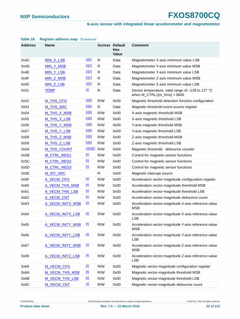
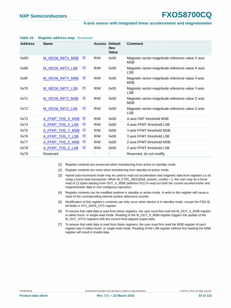
[1] Register contents are preserved when transitioning from active-to-standby mode.
[2] Register contents are reset when transitioning from standby-to-active mode.
[3] Hybrid auto-increment mode may be used to read out acceleration and magnetic data from registers x1-x6 using a burst-read transaction. When M_CTRL_REG2[hyb_autoinc_mode] = 1, the user may do a burst read of 12 bytes starting from OUT_X_MSB (address 0x1) to read out both the current accelerometer and magnetometer data in one contiguous operation.
[4] Register contents can be modified anytime in standby or active mode. A write to this register will cause a reset of the corresponding internal system debounce counter.
[5] Modification of this register’s contents can only occur when device is in standby mode, except the FS[1:0] bit fields in XYZ_DATA_CFG register.
[6] To ensure that valid data is read from these registers, the user must first read the M_OUT_X_MSB register in either burst- or single-read mode. Reading of the M_OUT_X_MSB register triggers the update of the M_OUT_X/Y/Z registers with the current time-aligned output data.
[7] To ensure that valid data is read from these registers, the user must first read the MSB register of each register pair in either burst- or single-read mode. Reading of the LSB register without first reading the MSB register will result in invalid data.
0x6D M_VECM_INITX_MSB [4] R/W 0x00 Magnetic vector-magnitude reference value X-axis MSB
0x6E M_VECM_INITX_LSB [4] R/W 0x00 Magnetic vector-magnitude reference value X-axis LSB
0x6F M_VECM_INITY_MSB [4] R/W 0x00 Magnetic vector-magnitude reference value Y-axis MSB
0x70 M_VECM_INITY_LSB [4] R/W 0x00 Magnetic vector-magnitude reference value Y-axis LSB
0x71 M_VECM_INITZ_MSB [4] R/W 0x00 Magnetic vector-magnitude reference value Z-axis MSB
0x72 M_VECM_INITZ_LSB [4] R/W 0x00 Magnetic vector-magnitude reference value Z-axis LSB
0x73 A_FFMT_THS_X_MSB [4] R/W 0x00 X-axis FMT threshold MSB
0x74 A_FFMT_THS_X_LSB [4] R/W 0x00 X-axis FFMT threshold LSB
0x75 A_FFMT_THS_Y_MSB [4] R/W 0x00 Y-axis FFMT threshold MSB
0x76 A_FFMT_THS_Y_LSB [4] R/W 0x00 Y-axis FFMT threshold LSB
0x77 A_FFMT_THS_Z_MSB [4] R/W 0x00 Z-axis FFMT threshold MSB
0x78 A_FFMT_THS_Z_LSB [4] R/W 0x00 Z-axis FFMT threshold LSB
0x79 Reserved - - Reserved, do not modify
Table 16. Register address map - ¶continued
Address Name Access DefaultHexValue
Comment
FXOS8700CQ All information provided in this document is subject to legal disclaimers. © NXP B.V. 2016. All rights reserved.
Product data sheet Rev. 7.0 — 22 March 2016 33 of 113
NXP Semiconductors FXOS8700CQ6-axis sensor with integrated linear accelerometer and magnetometer
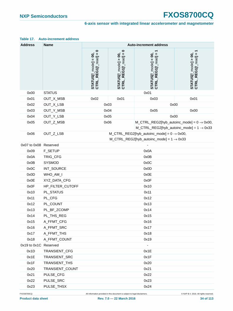
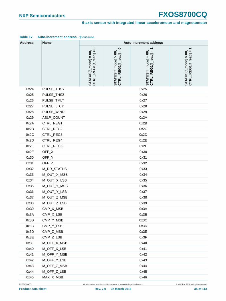
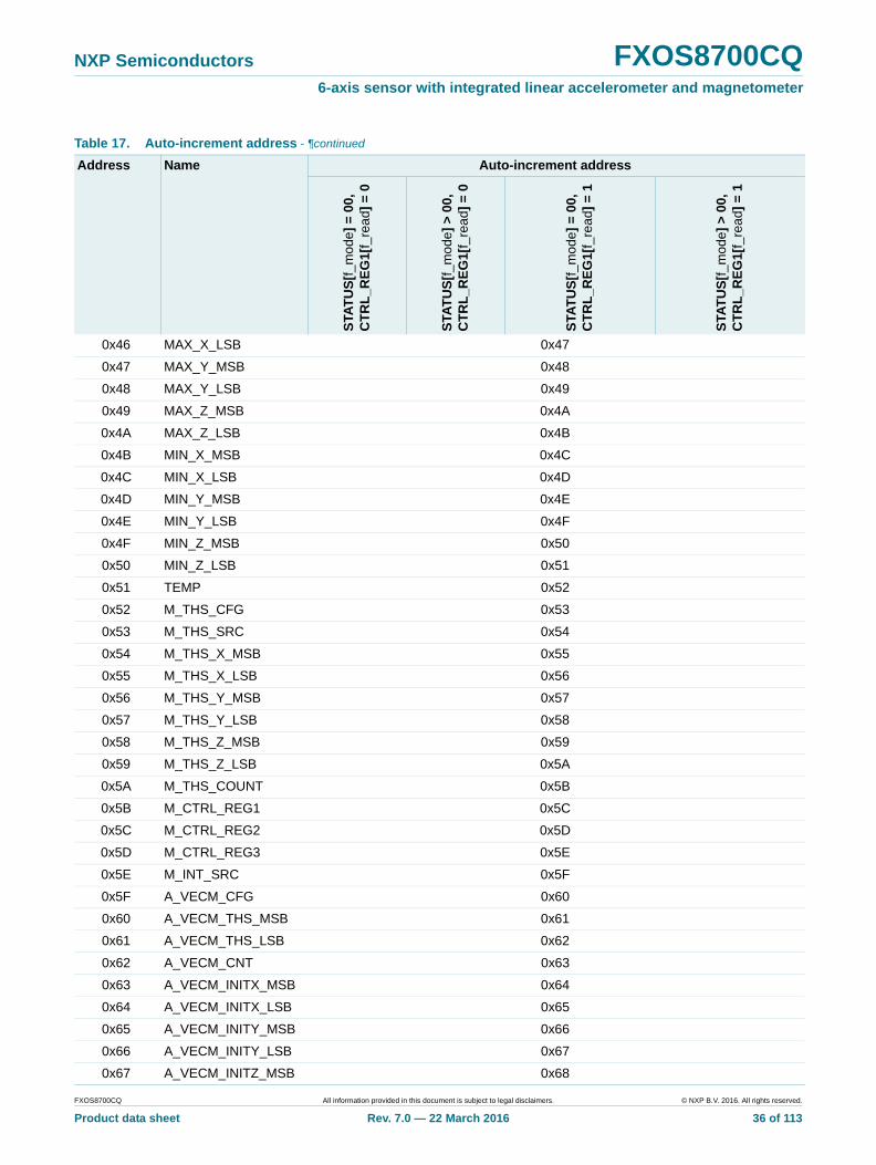
Table 17. Auto-increment address
Address Name Auto-increment address
STA
TU
S[f
_mod
e] =
00,
CT
RL
_RE
G1[
f_re
ad]
= 0
STA
TU
S[f
_mod
e] >
00,
CT
RL
_RE
G1[
f_re
ad]
= 0
STA
TU
S[f
_mod
e] =
00,
CT
RL
_RE
G1[
f_re
ad]
= 1
STA
TU
S[f
_mod
e] >
00,
CT
RL
_RE
G1[
f_re
ad]
= 1
0x00 STATUS 0x01
0x01 OUT_X_MSB 0x02 0x01 0x03 0x01
0x02 OUT_X_LSB 0x03 0x00
0x03 OUT_Y_MSB 0x04 0x05 0x00
0x04 OUT_Y_LSB 0x05 0x00
0x05 OUT_Z_MSB 0x06 M_CTRL_REG2[hyb_autoinc_mode] = 0 → 0x00,
M_CTRL_REG2[hyb_autoinc_mode] = 1 → 0x33
0x06 OUT_Z_LSB M_CTRL_REG2[hyb_autoinc_mode] = 0 → 0x00,
M_CTRL_REG2[hyb_autoinc_mode] = 1 → 0x33
0x07 to 0x08 Reserved -
0x09 F_SETUP 0x0A
0x0A TRIG_CFG 0x0B
0x0B SYSMOD 0x0C
0x0C INT_SOURCE 0x0D
0x0D WHO_AM_I 0x0E
0x0E XYZ_DATA_CFG 0x0F
0x0F HP_FILTER_CUTOFF 0x10
0x10 PL_STATUS 0x11
0x11 PL_CFG 0x12
0x12 PL_COUNT 0x13
0x13 PL_BF_ZCOMP 0x14
0x14 PL_THS_REG 0x15
0x15 A_FFMT_CFG 0x16
0x16 A_FFMT_SRC 0x17
0x17 A_FFMT_THS 0x18
0x18 A_FFMT_COUNT 0x19
0x19 to 0x1C Reserved -
0x1D TRANSIENT_CFG 0x1E
0x1E TRANSIENT_SRC 0x1F
0x1F TRANSIENT_THS 0x20
0x20 TRANSIENT_COUNT 0x21
0x21 PULSE_CFG 0x22
0x22 PULSE_SRC 0x23
0x23 PULSE_THSX 0x24
FXOS8700CQ All information provided in this document is subject to legal disclaimers. © NXP B.V. 2016. All rights reserved.
Product data sheet Rev. 7.0 — 22 March 2016 34 of 113
NXP Semiconductors FXOS8700CQ6-axis sensor with integrated linear accelerometer and magnetometer
0x24 PULSE_THSY 0x25
0x25 PULSE_THSZ 0x26
0x26 PULSE_TMLT 0x27
0x27 PULSE_LTCY 0x28
0x28 PULSE_WIND 0x29
0x29 ASLP_COUNT 0x2A
0x2A CTRL_REG1 0x2B
0x2B CTRL_REG2 0x2C
0x2C CTRL_REG3 0x2D
0x2D CTRL_REG4 0x2E
0x2E CTRL_REG5 0x2F
0x2F OFF_X 0x30
0x30 OFF_Y 0x31
0x31 OFF_Z 0x32
0x32 M_DR_STATUS 0x33
0x33 M_OUT_X_MSB 0x34
0x34 M_OUT_X_LSB 0x35
0x35 M_OUT_Y_MSB 0x36
0x36 M_OUT_Y_LSB 0x37
0x37 M_OUT_Z_MSB 0x38
0x38 M_OUT_Z_LSB 0x39
0x39 CMP_X_MSB 0x3A
0x3A CMP_X_LSB 0x3B
0x3B CMP_Y_MSB 0x3C
0x3C CMP_Y_LSB 0x3D
0x3D CMP_Z_MSB 0x3E
0x3E CMP_Z_LSB 0x3F
0x3F M_OFF_X_MSB 0x40
0x40 M_OFF_X_LSB 0x41
0x41 M_OFF_Y_MSB 0x42
0x42 M_OFF_Y_LSB 0x43
0x43 M_OFF_Z_MSB 0x44
0x44 M_OFF_Z_LSB 0x45
0x45 MAX_X_MSB 0x46
Table 17. Auto-increment address - ¶continued
Address Name Auto-increment address
STA
TU
S[f
_m
ode
] =
00,
CT
RL
_RE
G1[
f_re
ad]
= 0
STA
TU
S[f
_m
ode
] >
00,
CT
RL
_RE
G1[
f_re
ad]
= 0
STA
TU
S[f
_m
ode
] =
00,
CT
RL
_RE
G1[
f_re
ad]
= 1
STA
TU
S[f
_m
ode
] >
00,
CT
RL
_RE
G1[
f_re
ad]
= 1
FXOS8700CQ All information provided in this document is subject to legal disclaimers. © NXP B.V. 2016. All rights reserved.
Product data sheet Rev. 7.0 — 22 March 2016 35 of 113
NXP Semiconductors FXOS8700CQ6-axis sensor with integrated linear accelerometer and magnetometer
0x46 MAX_X_LSB 0x47
0x47 MAX_Y_MSB 0x48
0x48 MAX_Y_LSB 0x49
0x49 MAX_Z_MSB 0x4A
0x4A MAX_Z_LSB 0x4B
0x4B MIN_X_MSB 0x4C
0x4C MIN_X_LSB 0x4D
0x4D MIN_Y_MSB 0x4E
0x4E MIN_Y_LSB 0x4F
0x4F MIN_Z_MSB 0x50
0x50 MIN_Z_LSB 0x51
0x51 TEMP 0x52
0x52 M_THS_CFG 0x53
0x53 M_THS_SRC 0x54
0x54 M_THS_X_MSB 0x55
0x55 M_THS_X_LSB 0x56
0x56 M_THS_Y_MSB 0x57
0x57 M_THS_Y_LSB 0x58
0x58 M_THS_Z_MSB 0x59
0x59 M_THS_Z_LSB 0x5A
0x5A M_THS_COUNT 0x5B
0x5B M_CTRL_REG1 0x5C
0x5C M_CTRL_REG2 0x5D
0x5D M_CTRL_REG3 0x5E
0x5E M_INT_SRC 0x5F
0x5F A_VECM_CFG 0x60
0x60 A_VECM_THS_MSB 0x61
0x61 A_VECM_THS_LSB 0x62
0x62 A_VECM_CNT 0x63
0x63 A_VECM_INITX_MSB 0x64
0x64 A_VECM_INITX_LSB 0x65
0x65 A_VECM_INITY_MSB 0x66
0x66 A_VECM_INITY_LSB 0x67
0x67 A_VECM_INITZ_MSB 0x68
Table 17. Auto-increment address - ¶continued
Address Name Auto-increment address
STA
TU
S[f
_m
ode
] =
00,
CT
RL
_RE
G1[
f_re
ad]
= 0
STA
TU
S[f
_m
ode
] >
00,
CT
RL
_RE
G1[
f_re
ad]
= 0
STA
TU
S[f
_m
ode
] =
00,
CT
RL
_RE
G1[
f_re
ad]
= 1
STA
TU
S[f
_m
ode
] >
00,
CT
RL
_RE
G1[
f_re
ad]
= 1
FXOS8700CQ All information provided in this document is subject to legal disclaimers. © NXP B.V. 2016. All rights reserved.
Product data sheet Rev. 7.0 — 22 March 2016 36 of 113
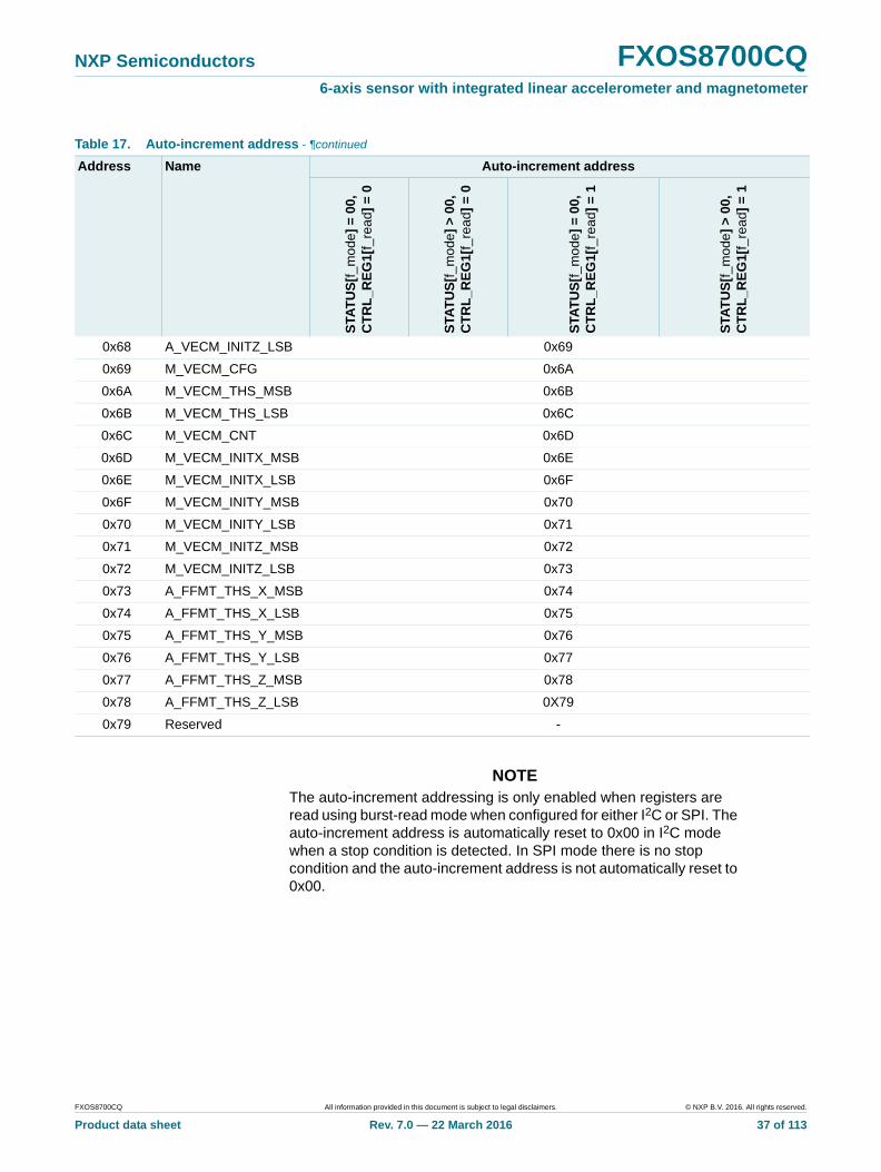
NXP Semiconductors FXOS8700CQ6-axis sensor with integrated linear accelerometer and magnetometer
NOTEThe auto-increment addressing is only enabled when registers are read using burst-read mode when configured for either I2C or SPI. The auto-increment address is automatically reset to 0x00 in I2C mode when a stop condition is detected. In SPI mode there is no stop condition and the auto-increment address is not automatically reset to 0x00.
0x68 A_VECM_INITZ_LSB 0x69
0x69 M_VECM_CFG 0x6A
0x6A M_VECM_THS_MSB 0x6B
0x6B M_VECM_THS_LSB 0x6C
0x6C M_VECM_CNT 0x6D
0x6D M_VECM_INITX_MSB 0x6E
0x6E M_VECM_INITX_LSB 0x6F
0x6F M_VECM_INITY_MSB 0x70
0x70 M_VECM_INITY_LSB 0x71
0x71 M_VECM_INITZ_MSB 0x72
0x72 M_VECM_INITZ_LSB 0x73
0x73 A_FFMT_THS_X_MSB 0x74
0x74 A_FFMT_THS_X_LSB 0x75
0x75 A_FFMT_THS_Y_MSB 0x76
0x76 A_FFMT_THS_Y_LSB 0x77
0x77 A_FFMT_THS_Z_MSB 0x78
0x78 A_FFMT_THS_Z_LSB 0X79
0x79 Reserved -
Table 17. Auto-increment address - ¶continued
Address Name Auto-increment address
STA
TU
S[f
_m
ode
] =
00,
CT
RL
_RE
G1[
f_re
ad]
= 0
STA
TU
S[f
_m
ode
] >
00,
CT
RL
_RE
G1[
f_re
ad]
= 0
STA
TU
S[f
_m
ode
] =
00,
CT
RL
_RE
G1[
f_re
ad]
= 1
STA
TU
S[f
_m
ode
] >
00,
CT
RL
_RE
G1[
f_re
ad]
= 1
FXOS8700CQ All information provided in this document is subject to legal disclaimers. © NXP B.V. 2016. All rights reserved.
Product data sheet Rev. 7.0 — 22 March 2016 37 of 113
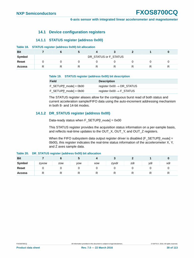
NXP Semiconductors FXOS8700CQ6-axis sensor with integrated linear accelerometer and magnetometer
14.1 Device configuration registers
14.1.1 STATUS register (address 0x00)
The STATUS register aliases allow for the contiguous burst read of both status and current acceleration sample/FIFO data using the auto-increment addressing mechanism in both 8- and 14-bit modes.
14.1.2 DR_STATUS register (address 0x00)
Data-ready status when F_SETUP[f_mode] = 0x00
This STATUS register provides the acquisition status information on a per-sample basis, and reflects real-time updates to the OUT_X, OUT_Y, and OUT_Z registers.
When the FIFO subsystem data output register driver is disabled (F_SETUP[f_mode] = 0b00), this register indicates the real-time status information of the accelerometer X, Y, and Z axes sample data.
Table 18. STATUS register (address 0x00) bit allocation
Bit 7 6 5 4 3 2 1 0
Symbol DR_STATUS or F_STATUS
Reset 0 0 0 0 0 0 0 0
Access R R R R R R R R
Table 19. STATUS register (address 0x00) bit description
Field Description
F_SETUP[f_mode] = 0b00 register 0x00 → DR_STATUS
F_SETUP[f_mode] > 0b00 register 0x00 → F_STATUS
Table 20. DR_STATUS register (address 0x00) bit allocation
Bit 7 6 5 4 3 2 1 0
Symbol zyxow zow yow xow zyxdr zdr ydr xdr
Reset 0 0 0 0 0 0 0 0
Access R R R R R R R R
FXOS8700CQ All information provided in this document is subject to legal disclaimers. © NXP B.V. 2016. All rights reserved.
Product data sheet Rev. 7.0 — 22 March 2016 38 of 113
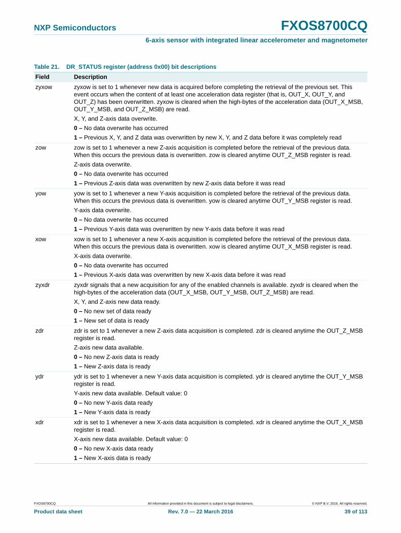
NXP Semiconductors FXOS8700CQ6-axis sensor with integrated linear accelerometer and magnetometer
Table 21. DR_STATUS register (address 0x00) bit descriptions
Field Description
zyxow zyxow is set to 1 whenever new data is acquired before completing the retrieval of the previous set. This event occurs when the content of at least one acceleration data register (that is, OUT_X, OUT_Y, and OUT_Z) has been overwritten. zyxow is cleared when the high-bytes of the acceleration data (OUT_X_MSB, OUT_Y_MSB, and OUT_Z_MSB) are read.
X, Y, and Z-axis data overwrite.
0 – No data overwrite has occurred
1 – Previous X, Y, and Z data was overwritten by new X, Y, and Z data before it was completely read
zow zow is set to 1 whenever a new Z-axis acquisition is completed before the retrieval of the previous data. When this occurs the previous data is overwritten. zow is cleared anytime OUT_Z_MSB register is read.
Z-axis data overwrite.
0 – No data overwrite has occurred
1 – Previous Z-axis data was overwritten by new Z-axis data before it was read
yow yow is set to 1 whenever a new Y-axis acquisition is completed before the retrieval of the previous data. When this occurs the previous data is overwritten. yow is cleared anytime OUT_Y_MSB register is read.
Y-axis data overwrite.
0 – No data overwrite has occurred
1 – Previous Y-axis data was overwritten by new Y-axis data before it was read
xow xow is set to 1 whenever a new X-axis acquisition is completed before the retrieval of the previous data. When this occurs the previous data is overwritten. xow is cleared anytime OUT_X_MSB register is read.
X-axis data overwrite.
0 – No data overwrite has occurred
1 – Previous X-axis data was overwritten by new X-axis data before it was read
zyxdr zyxdr signals that a new acquisition for any of the enabled channels is available. zyxdr is cleared when the high-bytes of the acceleration data (OUT_X_MSB, OUT_Y_MSB, OUT_Z_MSB) are read.
X, Y, and Z-axis new data ready.
0 – No new set of data ready
1 – New set of data is ready
zdr zdr is set to 1 whenever a new Z-axis data acquisition is completed. zdr is cleared anytime the OUT_Z_MSB register is read.
Z-axis new data available.
0 – No new Z-axis data is ready
1 – New Z-axis data is ready
ydr ydr is set to 1 whenever a new Y-axis data acquisition is completed. ydr is cleared anytime the OUT_Y_MSB register is read.
Y-axis new data available. Default value: 0
0 – No new Y-axis data ready
1 – New Y-axis data is ready
xdr xdr is set to 1 whenever a new X-axis data acquisition is completed. xdr is cleared anytime the OUT_X_MSB register is read.
X-axis new data available. Default value: 0
0 – No new X-axis data ready
1 – New X-axis data is ready
FXOS8700CQ All information provided in this document is subject to legal disclaimers. © NXP B.V. 2016. All rights reserved.
Product data sheet Rev. 7.0 — 22 March 2016 39 of 113
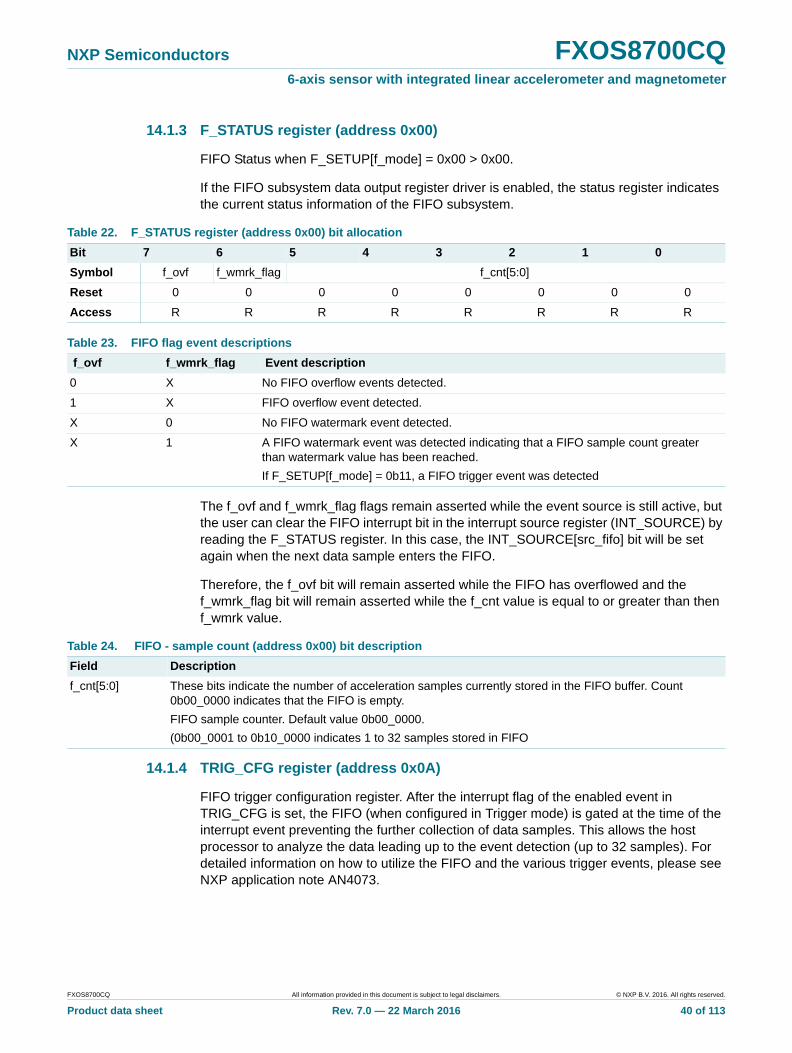
NXP Semiconductors FXOS8700CQ6-axis sensor with integrated linear accelerometer and magnetometer
14.1.3 F_STATUS register (address 0x00)
FIFO Status when F_SETUP[f_mode] = 0x00 > 0x00.
If the FIFO subsystem data output register driver is enabled, the status register indicates the current status information of the FIFO subsystem.
The f_ovf and f_wmrk_flag flags remain asserted while the event source is still active, but the user can clear the FIFO interrupt bit in the interrupt source register (INT_SOURCE) by reading the F_STATUS register. In this case, the INT_SOURCE[src_fifo] bit will be set again when the next data sample enters the FIFO.
Therefore, the f_ovf bit will remain asserted while the FIFO has overflowed and the f_wmrk_flag bit will remain asserted while the f_cnt value is equal to or greater than then f_wmrk value.
14.1.4 TRIG_CFG register (address 0x0A)
FIFO trigger configuration register. After the interrupt flag of the enabled event in TRIG_CFG is set, the FIFO (when configured in Trigger mode) is gated at the time of the interrupt event preventing the further collection of data samples. This allows the host processor to analyze the data leading up to the event detection (up to 32 samples). For detailed information on how to utilize the FIFO and the various trigger events, please see NXP application note AN4073.
Table 22. F_STATUS register (address 0x00) bit allocation
Bit 7 6 5 4 3 2 1 0
Symbol f_ovf f_wmrk_flag f_cnt[5:0]
Reset 0 0 0 0 0 0 0 0
Access R R R R R R R R
Table 23. FIFO flag event descriptions
f_ovf f_wmrk_flag Event description
0 X No FIFO overflow events detected.
1 X FIFO overflow event detected.
X 0 No FIFO watermark event detected.
X 1 A FIFO watermark event was detected indicating that a FIFO sample count greater than watermark value has been reached.
If F_SETUP[f_mode] = 0b11, a FIFO trigger event was detected
Table 24. FIFO - sample count (address 0x00) bit description
Field Description
f_cnt[5:0] These bits indicate the number of acceleration samples currently stored in the FIFO buffer. Count 0b00_0000 indicates that the FIFO is empty.
FIFO sample counter. Default value 0b00_0000.
(0b00_0001 to 0b10_0000 indicates 1 to 32 samples stored in FIFO
FXOS8700CQ All information provided in this document is subject to legal disclaimers. © NXP B.V. 2016. All rights reserved.
Product data sheet Rev. 7.0 — 22 March 2016 40 of 113
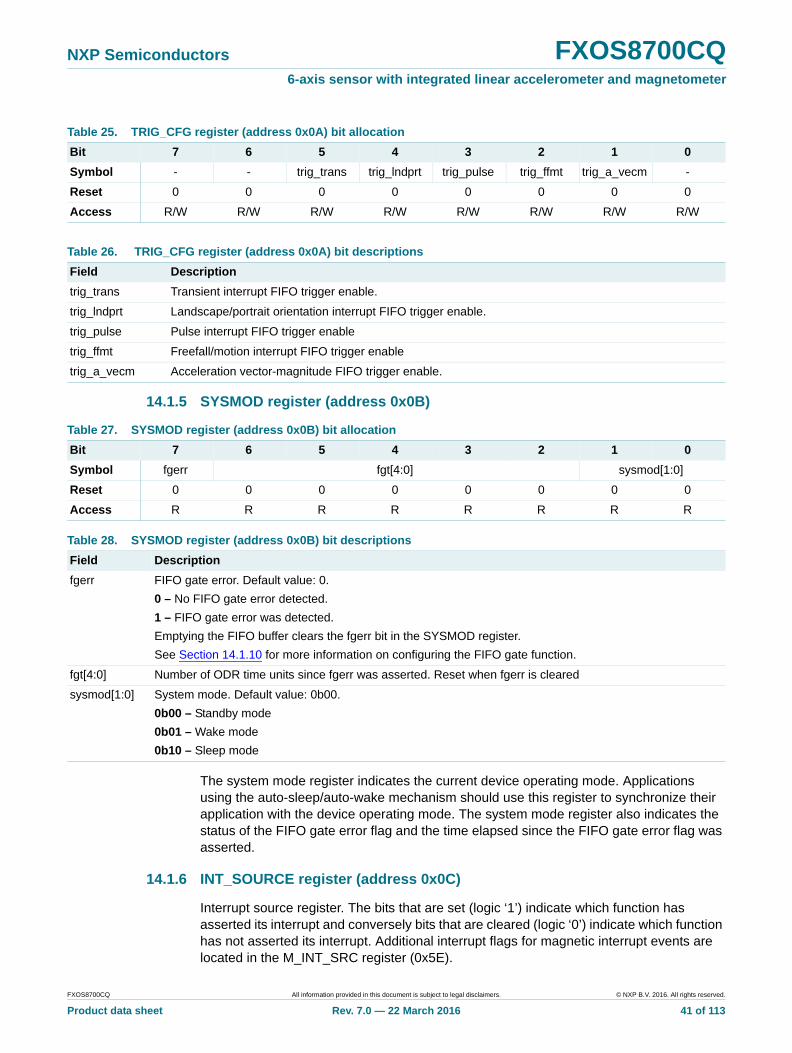
NXP Semiconductors FXOS8700CQ6-axis sensor with integrated linear accelerometer and magnetometer
14.1.5 SYSMOD register (address 0x0B)
The system mode register indicates the current device operating mode. Applications using the auto-sleep/auto-wake mechanism should use this register to synchronize their application with the device operating mode. The system mode register also indicates the status of the FIFO gate error flag and the time elapsed since the FIFO gate error flag was asserted.
14.1.6 INT_SOURCE register (address 0x0C)
Interrupt source register. The bits that are set (logic ‘1’) indicate which function has asserted its interrupt and conversely bits that are cleared (logic ‘0’) indicate which function has not asserted its interrupt. Additional interrupt flags for magnetic interrupt events are located in the M_INT_SRC register (0x5E).
Table 25. TRIG_CFG register (address 0x0A) bit allocation
Bit 7 6 5 4 3 2 1 0
Symbol - - trig_trans trig_lndprt trig_pulse trig_ffmt trig_a_vecm -
Reset 0 0 0 0 0 0 0 0
Access R/W R/W R/W R/W R/W R/W R/W R/W
Table 26. TRIG_CFG register (address 0x0A) bit descriptions
Field Description
trig_trans Transient interrupt FIFO trigger enable.
trig_lndprt Landscape/portrait orientation interrupt FIFO trigger enable.
trig_pulse Pulse interrupt FIFO trigger enable
trig_ffmt Freefall/motion interrupt FIFO trigger enable
trig_a_vecm Acceleration vector-magnitude FIFO trigger enable.
Table 27. SYSMOD register (address 0x0B) bit allocation
Bit 7 6 5 4 3 2 1 0
Symbol fgerr fgt[4:0] sysmod[1:0]
Reset 0 0 0 0 0 0 0 0
Access R R R R R R R R
Table 28. SYSMOD register (address 0x0B) bit descriptions
Field Description
fgerr FIFO gate error. Default value: 0.
0 – No FIFO gate error detected.
1 – FIFO gate error was detected.
Emptying the FIFO buffer clears the fgerr bit in the SYSMOD register.
See Section 14.1.10 for more information on configuring the FIFO gate function.
fgt[4:0] Number of ODR time units since fgerr was asserted. Reset when fgerr is cleared
sysmod[1:0] System mode. Default value: 0b00.
0b00 – Standby mode
0b01 – Wake mode
0b10 – Sleep mode
FXOS8700CQ All information provided in this document is subject to legal disclaimers. © NXP B.V. 2016. All rights reserved.
Product data sheet Rev. 7.0 — 22 March 2016 41 of 113
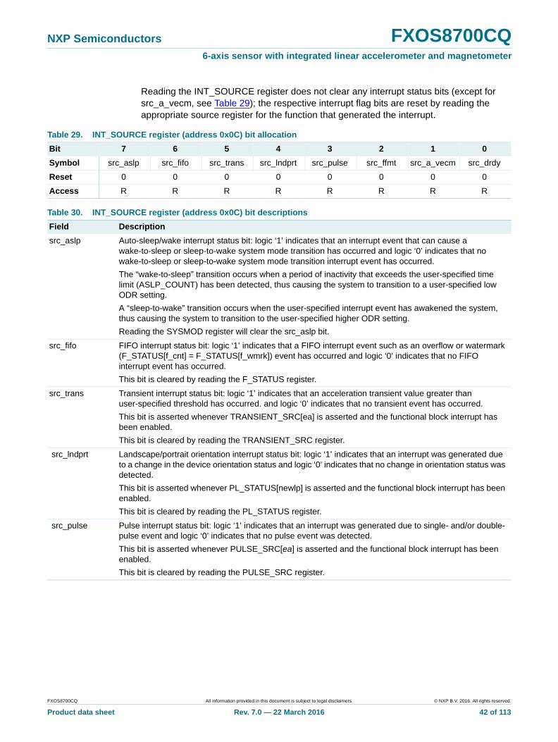
NXP Semiconductors FXOS8700CQ6-axis sensor with integrated linear accelerometer and magnetometer
Reading the INT_SOURCE register does not clear any interrupt status bits (except for src_a_vecm, see Table 29); the respective interrupt flag bits are reset by reading the appropriate source register for the function that generated the interrupt.
Table 29. INT_SOURCE register (address 0x0C) bit allocation
Bit 7 6 5 4 3 2 1 0
Symbol src_aslp src_fifo src_trans src_lndprt src_pulse src_ffmt src_a_vecm src_drdy
Reset 0 0 0 0 0 0 0 0
Access R R R R R R R R
Table 30. INT_SOURCE register (address 0x0C) bit descriptions
Field Description
src_aslp Auto-sleep/wake interrupt status bit: logic ‘1’ indicates that an interrupt event that can cause a wake-to-sleep or sleep-to-wake system mode transition has occurred and logic ‘0’ indicates that no wake-to-sleep or sleep-to-wake system mode transition interrupt event has occurred.
The “wake-to-sleep” transition occurs when a period of inactivity that exceeds the user-specified time limit (ASLP_COUNT) has been detected, thus causing the system to transition to a user-specified low ODR setting.
A “sleep-to-wake” transition occurs when the user-specified interrupt event has awakened the system, thus causing the system to transition to the user-specified higher ODR setting.
Reading the SYSMOD register will clear the src_aslp bit.
src_fifo FIFO interrupt status bit: logic ‘1’ indicates that a FIFO interrupt event such as an overflow or watermark (F_STATUS[f_cnt] = F_STATUS[f_wmrk]) event has occurred and logic ‘0’ indicates that no FIFO interrupt event has occurred.
This bit is cleared by reading the F_STATUS register.
src_trans Transient interrupt status bit: logic ‘1’ indicates that an acceleration transient value greater than user-specified threshold has occurred. and logic ‘0’ indicates that no transient event has occurred.
This bit is asserted whenever TRANSIENT_SRC[ea] is asserted and the functional block interrupt has been enabled.
This bit is cleared by reading the TRANSIENT_SRC register.
src_lndprt Landscape/portrait orientation interrupt status bit: logic ‘1’ indicates that an interrupt was generated due to a change in the device orientation status and logic ‘0’ indicates that no change in orientation status was detected.
This bit is asserted whenever PL_STATUS[newlp] is asserted and the functional block interrupt has been enabled.
This bit is cleared by reading the PL_STATUS register.
src_pulse Pulse interrupt status bit: logic ‘1’ indicates that an interrupt was generated due to single- and/or double- pulse event and logic ‘0’ indicates that no pulse event was detected.
This bit is asserted whenever PULSE_SRC[ea] is asserted and the functional block interrupt has been enabled.
This bit is cleared by reading the PULSE_SRC register.
FXOS8700CQ All information provided in this document is subject to legal disclaimers. © NXP B.V. 2016. All rights reserved.
Product data sheet Rev. 7.0 — 22 March 2016 42 of 113
NXP Semiconductors FXOS8700CQ6-axis sensor with integrated linear accelerometer and magnetometer
14.1.7 WHO_AM_I register (address 0x0D)
Device identification register. This register contains the device identifier which is set to 0xC4 for preproduction devices and 0xC7 for production devices.
14.1.8 CTRL_REG1 register (address 0x0A)
NOTEExcept for standby mode selection, the device must be in standby mode to change any of the fields within CTRL_REG1 (0x2A).
src_ffmt Freefall/motion interrupt status bit: logic ‘1’ indicates that the freefall/motion function interrupt is active and logic ‘0’ indicates that no freefall or motion event was detected.
This bit is asserted whenever A_FFMT_SRC[ea] is asserted and the functional block interrupt has been enabled.
This bit is cleared by reading the A_FFMT_SRC register.
src_a_vecm Accelerometer vector-magnitude interrupt status bit: logic ‘1’ indicates that an interrupt was generated due to acceleration vector-magnitude function and logic ‘0’ indicates that no interrupt has been generated. This bit is cleared by reading this register (INT_SOURCE).
src_drdy Data-ready interrupt status bit. In acceleration only mode this bit indicates that new accelerometer data is available to read. In magnetometer only mode, src_drdy indicates that new magnetic data is available to be read. In hybrid mode, this bit signals that new acceleration and/or magnetic data is available.
The src_drdy interrupt flag is cleared by reading out the acceleration data in accelerometer only mode and by reading out the magnetic data in magnetometer only or hybrid modes. In hybrid mode and with M_CTRL_REG2[hyb_autoinc_mode] = 1, all of the sensor data can be read out in a 12-byte burst read starting at register 0x01 (OUT_X_MSB).
Table 30. INT_SOURCE register (address 0x0C) bit descriptions - ¶continued
Field Description
Table 31. WHO_AM_I register (address 0x0D) bit allocation
Bit 7 6 5 4 3 2 1 0
Symbol who_am_i[7:0]
Reset 1 1 0 0 0 1 1 1
Access R R R R R R R R
Table 32. CTRL_REG1 register (address 0x0A) bit allocation
Bit 7 6 5 4 3 2 1 0
Symbol aslp_rate[1:0] dr[2:0] lnoise f_read active
Reset 0 0 0 0 0 0 0 0
Access R/W R/W R/W R/W R/W R/W R/W R/W
FXOS8700CQ All information provided in this document is subject to legal disclaimers. © NXP B.V. 2016. All rights reserved.
Product data sheet Rev. 7.0 — 22 March 2016 43 of 113
NXP Semiconductors FXOS8700CQ6-axis sensor with integrated linear accelerometer and magnetometer
It is important to note that when the device is in auto-sleep mode, the system ODR and data rate for all the system functional blocks is overridden by the sleep data rate set by the aslp_rate field. When hybrid mode is enabled, the frequency is one-half of what is shown in Table 35. For example, with aslp_rate = 0b00 the frequency is 25 Hz.
Table 35 shows the various system output data rates (ODR) that may be selected using the dr[2:0] bits.The selected ODR is reduced by a factor of two when the device is operated in hybrid mode.
Table 33. CTRL_REG1 register (address 0x0A) bit descriptions
Field Description
aslp_rate[1:0] Configures the auto-wake sample frequency when the device is in sleep mode.
See Table 35 for more information.
dr[2:0] Output data rate (ODR) selection.
See Table 35 for more information.
lnoise Reduced noise and full-scale range mode (analog gain times 2).
0 – Normal mode
1 – Reduced noise mode; Note that the FSR setting is restricted to ±2 g or ±4 g mode. This feature cannot be used in ±8 g mode.
f_read Fast-read mode: Data format is limited to the 8-bit MSB for accelerometer output data. The auto-address pointer will skip over the LSB addresses for each axes sample data when performing a burst-read operation.
0 – Normal mode
1 – Fast-read mode
active Standby/active.
0 – Standby mode
1 – Active mode
Table 34. Sleep mode ODR selection
aslp_rate[1] aslp_rate[0] Frequency (Hz)
0 0 50
0 1 12.5
1 0 6.25
1 1 1.56
Table 35. System Output Data Rate selection
dr[2] dr[2] dr[2] ODR accelerometer or magnetometer only modes (Hz)
Period accelerometer or magnetometer only modes (ms)
ODR hybrid mode (Hz)
Period hybrid mode (ms)
0 0 0 800.0 1.25 400 2.5
0 0 1 400.0 2.5 200 5
0 1 0 200.0 5 100 10
0 1 1 100.0 10 50 20
1 0 0 50.0 20 25 80
1 0 1 12.5 80 6.25 160
1 1 0 6.25 160 3.125 320
1 1 1 1.5625 640 0.7813 1280
FXOS8700CQ All information provided in this document is subject to legal disclaimers. © NXP B.V. 2016. All rights reserved.
Product data sheet Rev. 7.0 — 22 March 2016 44 of 113
NXP Semiconductors FXOS8700CQ6-axis sensor with integrated linear accelerometer and magnetometer
The active bit selects between standby mode and active mode. The default value is 0 (standby mode) on reset.
The lnoise bit selects between normal full dynamic range mode and a high sensitivity, low-noise mode. In low-noise mode the maximum signal that can be measured is ±4 g. Note: Any thresholds set above 4 g will not be reached.
The f_read bit selects between normal and fast-read modes where the auto-increment counter will also skip over the LSB data bytes when f_read = 1. In hybrid mode and with M_CTRL_REG2[hyb_autoinc_mode] = 1, all of the sensor data MSB's can be read out with a single 6-byte burst read starting at the OUT_X_MSB register.
NOTEThe f_read bit can only be changed while F_SETUP[f_mode] = 0.
14.1.9 CTRL_REG2 register (address 0x2B)
Table 36. CTRL_REG2 register (address 0x2B) bit allocation
Bit 7 6 5 4 3 2 1 0
Symbol st rst - smods[1:0] slpe mods[1:0]
Reset 0 0 0 0 0 0 0 0
Access R/W R/W R/W R/W R/W R/W R/W R/W
FXOS8700CQ All information provided in this document is subject to legal disclaimers. © NXP B.V. 2016. All rights reserved.
Product data sheet Rev. 7.0 — 22 March 2016 45 of 113
NXP Semiconductors FXOS8700CQ6-axis sensor with integrated linear accelerometer and magnetometer
[1] When slpe = 1, a transition between sleep mode and wake mode (or vice-versa) results in a FIFO flush and resets all of the internal functions debounce counters. All functional block status information is preserved except where otherwise indicated. For further information, refer to the CTRL_REG3 register description (fifo_gate bit).
Table 37. CTRL_REG2 register (address 0x2B) bit descriptions
Field Description
st The st bit activates the accelerometer self-test function. When st is set to 1, a change will occur in the device output levels for each axis, allowing the host application to check the functionality of the transducer and measurement signal chain.
Self-test enable:
0 – Self-test disabled
1 – Self-test enabled
rst The rst bit is used to initiate a software reset. The reset mechanism can be enabled in both standby and active modes. When the rst bit is set, the boot mechanism resets all functional block registers and loads the respective internal registers with their default values. Refer to document FXOS8700CQER for further information and a suggested work-around. After setting the rst bit, the system will automatically transition to standby mode. Therefore, if the system was already in standby mode, the reboot process will immediately begin; else if the system was in active mode the boot mechanism will automatically transition the system from active mode to standby mode, only then can the reboot process begin. A system reset can also be initiated by pulsing the external RST pin high.
The host application should allow 1 ms between issuing a software (setting rst bit) or hardware (pulsing RST pin) reset and attempting communications with the device over the I2C or SPI interfaces. When the SPI interface mode is desired and multiple devices are present on the bus, make sure that the bus is quiet (all slave device MISO pins are high-z) during this 1 ms period to ensure the device does not inadvertently enter I2C mode. See Section 10.2.3 for further information about the interface mode auto-detection circuit.
Note: The I2C and SPI communication systems are also reset to avoid corrupted data transactions. On issuing a software reset command over an I2C interface, the device immediately resets and does not send any acknowledgment (ACK) of the written byte to the master. The host application has to implement the I2C driver in such a way that it does not look for an ACK following a soft reset command.
At the end of the boot process, the rst bit is hardware cleared.
0 – Device reset disabled
1 – Device reset enabled
smods[1:0] Accelerometer sleep mode OSR mode selection. This setting, along with the CTRL_REG1[aslp_rate] ODR setting determines the sleep mode power and noise for acceleration measurements.
See Table 38 and Table 39 for more information.
slpe[1] Auto-sleep mode enable:
0 – Auto-sleep is not enabled
1 – Auto-sleep is enabled
mods[1:0] Accelerometer wake mode OSR mode selection. This setting, along with the ODR selection (CTRL_REG1[dr]) determines the wake mode power and noise for acceleration measurements. See Table 38 and Table 39 for more information.
Table 38. CTRL_REG2[(s)mods] oversampling modes
(s)mods[1] (s)mods[0] Power mode
0 0 Normal
0 1 Low noise, low power
1 0 High resolution
1 1 Low power
FXOS8700CQ All information provided in this document is subject to legal disclaimers. © NXP B.V. 2016. All rights reserved.
Product data sheet Rev. 7.0 — 22 March 2016 46 of 113
NXP Semiconductors FXOS8700CQ6-axis sensor with integrated linear accelerometer and magnetometer
14.1.10 CTRL_REG3 - interrupt control register (address 0x2C)
Table 39. Oversampling Ratio versus oversampling mode
Accelerometer OSR
ODR (Hz) Normal Low noise, low power High resolution Low power
1.5625 128 32 1024 16
6.25 32 8 256 4
12.5 16 4 128 2
50 4 4 32 2
100 4 4 16 2
200 4 4 8 2
400 4 4 4 2
800 2 2 2 2
Table 40. CTRL_REG3 - interrupt control register (address 0x2C) bit allocation
Bit 7 6 5 4 3 2 1 0
Symbol fifo_gate wake_trans wake_lndprt wake_pulse wake_ffmt wake_a_vecm ipol pp_od
Reset 0 0 0 0 0 0 0 0
Access R/W R/W R/W R/W R/W R/W R/W R/W
Table 41. CTRL_REG3 - interrupt control register (address 0x2C) bit descriptions
Field Description
fifo_gate 0 – FIFO gate is bypassed. FIFO is flushed upon the system mode transitioning from wake-to-sleep mode or from sleep-to-wake mode.
1 – The FIFO input buffer is blocked from accepting new samples when transitioning from “wake-to-sleep” mode or from “sleep-to-wake” mode until the FIFO is flushed [1]. Although the system transitions from “wake-to-sleep” or from “sleep-to-wake” the contents of the FIFO buffer are preserved and new data samples are ignored until the FIFO is emptied by the host application.
If the fifo_gate bit is set to logic ‘1’ and the FIFO buffer is not emptied before the arrival of the next sample, then the SYSMOD[fgerr] will be asserted. The SYSMOD[fgerr] bit remains asserted as long as the FIFO buffer remains un-emptied.
Emptying the FIFO buffer clears the SYS_MOD[fgerr] register.
wake_tran 0 – Transient function is disabled in sleep mode
1 – Transient function is enabled in sleep mode and can generate an interrupt to wake the system
wake_lndprt 0 – Orientation function is disabled sleep mode.
1 – Orientation function is enabled in sleep mode and can generate an interrupt to wake the system
wake_pulse 0 – Pulse function is disabled in sleep mode
1 – Pulse function is enabled in sleep mode and can generate an interrupt to wake the system
wake_ffmt 0 – Freefall/motion function is disabled in sleep mode
1 – Freefall/motion function is enabled in sleep mode and can generate an interrupt to wake the system
FXOS8700CQ All information provided in this document is subject to legal disclaimers. © NXP B.V. 2016. All rights reserved.
Product data sheet Rev. 7.0 — 22 March 2016 47 of 113
NXP Semiconductors FXOS8700CQ6-axis sensor with integrated linear accelerometer and magnetometer
[1] The FIFO contents are flushed whenever the system ODR changes in order to prevent the mixing of FIFO data from different ODR periods.
The wake enable bits for the magnetic threshold and magnetic vector-magnitude functions are located in registers 0x52 (MAG_THS_CFG) and 0x69 (M_VECM_CFG), respectively.
14.1.11 CTRL_REG4 - interrupt enable register (address 0x2D)
wake_a_vecm 0 – Acceleration vector-magnitude function is disabled in sleep mode
1 – Acceleration vector-magnitude function is enabled in sleep mode and can generate an interrupt to wake the system
ipol The ipol The bit selects the logic polarity of the interrupt signals output on the INT1 and INT2 pins.
INT1/INT2 interrupt logic polarity:
0 – Active low (default)
1 – Active high
pp_od INT1/INT2 push-pull or open-drain output mode selection. The open-drain configuration can be used for connecting multiple interrupt signals on the same interrupt line but will require an external pullup resistor to function correctly.
0 – Push-pull (default)
1 – Open drain
Table 41. CTRL_REG3 - interrupt control register (address 0x2C) bit descriptions - ¶continued
Field Description
Table 42. CTRL_REG4 - interrupt enable register (address 0x2D) bit allocation
Bit 7 6 5 4 3 2 1 0
Symbol int_en_aslp int_en_fifo int_en_trans int_en_lndprt int_en_pulse int_en_ffmt int_en_a_vecm int_en_drdy
Reset 0 0 0 0 0 0 0 0
Access R/W R/W R/W R/W R/W R/W R/W R/W
Table 43. CTRL_REG4 - interrupt enable register (address 0x2D) bit descriptions
Field Description
int_en_aslp Sleep interrupt enable
0 – Auto-sleep/wake interrupt disabled
1‘b1 – Auto-sleep/wake interrupt enabled
int_en_fifo FIFO interrupt enable
0 – FIFO interrupt disabled
1 – FIFO interrupt enabled
int_en_trans Transient interrupt enable
0 – Transient interrupt disabled
1 – Transient interrupt enabled
int_en_lndprt Orientation interrupt enable
0 – Orientation (landscape/portrait) interrupt disabled
1 – Orientation (landscape/portrait) interrupt enabled
int_en_pulse Pulse interrupt enable
0 – Pulse detection interrupt disabled
1 – Pulse detection interrupt enabled
FXOS8700CQ All information provided in this document is subject to legal disclaimers. © NXP B.V. 2016. All rights reserved.
Product data sheet Rev. 7.0 — 22 March 2016 48 of 113
NXP Semiconductors FXOS8700CQ6-axis sensor with integrated linear accelerometer and magnetometer
The corresponding functional block interrupt enable bit allows the functional block to route its event detection flag to the system’s interrupt controller. The interrupt controller routes the enabled interrupt signals to either the INT1 or INT2 pins depending on the settings made in CTRL_REG5. Please note that the interrupt enable bits for the magnetic threshold and vector-magnitude interrupts are located in registers 0x52 (MAG_THS_CFG), and 0x69 (M_VECM_CFG), respectively.
14.1.12 CTRL_REG5 - interrupt routing configuration register (address 0x2E)
int_en_ffmt Freefall/motion interrupt enable
0 – Freefall/motion interrupt disabled
1 – Freefall/motion interrupt enabled
int_en_a_vecm Acceleration vector-magnitude interrupt enable
0 – Acceleration vector-magnitude interrupt disabled
1 – Acceleration vector-magnitude interrupt enabled
int_en_drdy Data-ready interrupt enable
0 – Data-ready interrupt disabled
1 – Data-ready interrupt enabled
Table 43. CTRL_REG4 - interrupt enable register (address 0x2D) bit descriptions - ¶continued
Field Description
Table 44. CTRL_REG5 - interrupt routing configuration register (address 0x2E) bit allocation
Bit 7 6 5 4 3 2 1 0
Symbol int_cfg_aslp int_cfg_fifo int_cfg_trans int_cfg_lndprt int_cfg_pulse int_cfg_ffmt int_cfg_a_vecm int_cfg_drdy
Reset 0 0 0 0 0 0 0 0
Access R/W R/W R/W R/W R/W R/W R/W R/W
Table 45. CTRL_REG5 - interrupt routing configuration register (address 0x2E) bit descriptions
Field Description
int_cfg_aslp Sleep interrupt routing
0 – Interrupt is routed to INT2 pin
1 – Interrupt is routed to INT1 pin
int_cfg_fifo FIFO interrupt routing
0 – Interrupt is routed to INT2 pin
1 – Interrupt is routed to INT1 pin
int_cfg_trans Transient detection interrupt routing
0 – Interrupt is routed to INT2 pin
1 – Interrupt is routed to INT1 pin
int_cfg_lndprt Orientation detection interrupt routing
0 – Interrupt is routed to INT2 pin
1 – Interrupt is routed to INT1 pin
int_cfg_pulse Pulse detection interrupt routing
0 – Interrupt is routed to INT2 pin
1 – Interrupt is routed to INT1 pin
FXOS8700CQ All information provided in this document is subject to legal disclaimers. © NXP B.V. 2016. All rights reserved.
Product data sheet Rev. 7.0 — 22 March 2016 49 of 113
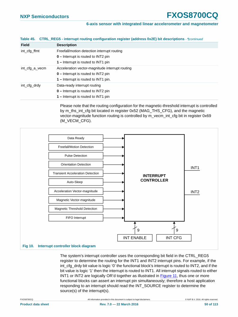
NXP Semiconductors FXOS8700CQ6-axis sensor with integrated linear accelerometer and magnetometer
Please note that the routing configuration for the magnetic-threshold interrupt is controlled by m_ths_int_cfg bit located in register 0x52 (MAG_THS_CFG), and the magnetic vector-magnitude function routing is controlled by m_vecm_int_cfg bit in register 0x69 (M_VECM_CFG).
The system’s interrupt controller uses the corresponding bit field in the CTRL_REG5 register to determine the routing for the INT1 and INT2 interrupt pins. For example, if the int_cfg_drdy bit value is logic ‘0’ the functional block’s interrupt is routed to INT2, and if the bit value is logic ‘1’ then the interrupt is routed to INT1. All interrupt signals routed to either INT1 or INT2 are logically OR’d together as illustrated in Figure 11, thus one or more functional blocks can assert an interrupt pin simultaneously; therefore a host application responding to an interrupt should read the INT_SOURCE register to determine the source(s) of the interrupt(s).
int_cfg_ffmt Freefall/motion detection interrupt routing
0 – Interrupt is routed to INT2 pin
1 – Interrupt is routed to INT1 pin
int_cfg_a_vecm Acceleration vector-magnitude interrupt routing
0 – Interrupt is routed to INT2 pin
1 – Interrupt is routed to INT1 pin.
int_cfg_drdy Data-ready interrupt routing
0 – Interrupt is routed to INT2 pin
1 – Interrupt is routed to INT1 pin
Table 45. CTRL_REG5 - interrupt routing configuration register (address 0x2E) bit descriptions - ¶continued
Field Description
Fig 10. Interrupt controller block diagram
INTERRUPTCONTROLLER
Data Ready
Freefall/Motion Detection
Pulse Detection
Orientation Detection
Transient Acceleration Detection
Auto-Sleep
INT ENABLE INT CFG
INT1
INT2
9 9
Acceleration Vector-magnitude
Magnetic Vector-magnitude
Magnetic Threshold Detection
FIFO Interrupt
FXOS8700CQ All information provided in this document is subject to legal disclaimers. © NXP B.V. 2016. All rights reserved.
Product data sheet Rev. 7.0 — 22 March 2016 50 of 113
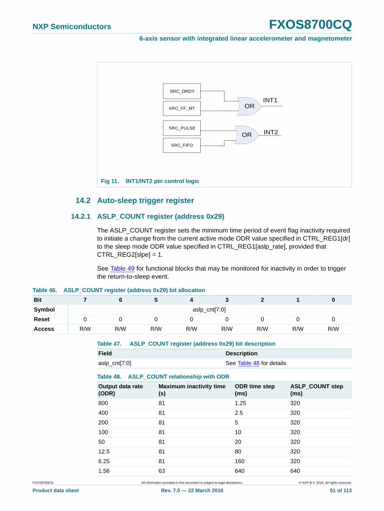
NXP Semiconductors FXOS8700CQ6-axis sensor with integrated linear accelerometer and magnetometer
14.2 Auto-sleep trigger register
14.2.1 ASLP_COUNT register (address 0x29)
The ASLP_COUNT register sets the minimum time period of event flag inactivity required to initiate a change from the current active mode ODR value specified in CTRL_REG1[dr] to the sleep mode ODR value specified in CTRL_REG1[aslp_rate], provided that CTRL_REG2[slpe] = 1.
See Table 49 for functional blocks that may be monitored for inactivity in order to trigger the return-to-sleep event.
Fig 11. INT1/INT2 pin control logic
INT1
INT2
SRC_RTS
SRC_FIFO
SRC_PULSE
SRC_FF_MT OR
OR
SRC_DRDY
Table 46. ASLP_COUNT register (address 0x29) bit allocation
Bit 7 6 5 4 3 2 1 0
Symbol aslp_cnt[7:0]
Reset 0 0 0 0 0 0 0 0
Access R/W R/W R/W R/W R/W R/W R/W R/W
Table 47. ASLP_COUNT register (address 0x29) bit description
Field Description
aslp_cnt[7:0] See Table 48 for details
Table 48. ASLP_COUNT relationship with ODR
Output data rate(ODR)
Maximum inactivity time(s)
ODR time step(ms)
ASLP_COUNT step(ms)
800 81 1.25 320
400 81 2.5 320
200 81 5 320
100 81 10 320
50 81 20 320
12.5 81 80 320
6.25 81 160 320
1.56 63 640 640
FXOS8700CQ All information provided in this document is subject to legal disclaimers. © NXP B.V. 2016. All rights reserved.
Product data sheet Rev. 7.0 — 22 March 2016 51 of 113
NXP Semiconductors FXOS8700CQ6-axis sensor with integrated linear accelerometer and magnetometer
Please note that when the device is operated in hybrid mode, the effective ODR is half of what is selected in CTRL_REG1[dr]. For example, with ODR = 800 Hz and the device set to hybrid mode, the ASLP_COUNT time step becomes 640 ms.
[1] If the fifo_gate bit is set to logic ‘1’, the assertion of the SRC_ASLP interrupt does not prevent the system from transitioning to sleep or from wake mode; instead it prevents the FIFO buffer from accepting new sample data until the host application flushes the FIFO buffer.
The interrupt sources listed in Table 49 affect the auto-sleep, return to sleep and wake from sleep mechanism only if they have been previously enabled. The functional block event flags that are bypassed while the system is in auto-sleep mode are temporary disabled (Section 14.1.10) and are automatically re-enabled when the device returns from auto-sleep mode (that is, wakes up), except for the data ready function.
If any of the interrupt sources listed under the return-to-sleep column is asserted before the sleep counter reaches the value specified in ASLP_COUNT, then all sleep mode transitions are terminated and the internal sleep counter is reset. If none of the interrupts listed under the return-to-sleep column are asserted within the time limit specified by the ASLP_COUNT register, the system will transition to the auto-sleep mode and use the ODR value specified in CTRL_REG1[aslp_rate].
If any of the interrupt sources listed under the “wake-from-sleep” column is asserted, then the system will transition out of the low sample rate auto-sleep mode to the user-specified wake mode sample rate provided that the specific wake event function is enabled in register CTRL_REG3.
If the auto-sleep interrupt is enabled, a transition from active mode to sleep mode and (vice-versa) will generate an interrupt.This interrupt is cleared by reading the SYSMOD (0x0B) register.
If CTRL_REG3[fifo_gate] = 1, a transition into auto-sleep mode will preserve the FIFO contents and set SYSMOD[fgerr] (FIFO gate error), and prevent the further collection of accelerometer data into the FIFO. The system will wait for the FIFO buffer to be emptied by the host application before new samples can be acquired.
Table 49. Sleep/wake mode gates and triggers
Interrupt source Event restarts time anddelays return-to-sleep
Event will wake-from-sleep
SRC_FIFO Yes No
SRC_TRANS Yes Yes
SRC_LNDPRT Yes Yes
SRC_PULSE Yes Yes
SRC_FFMT Yes Yes
SRC_ASLP No[1] No[1]
SRC_Mag Yes Yes
SRC_DRDY No No
SRC_AVECM Yes Yes
SRC_MVECM Yes Yes
SRC_MTHS Yes Yes
SRC_FIFO Yes No
FXOS8700CQ All information provided in this document is subject to legal disclaimers. © NXP B.V. 2016. All rights reserved.
Product data sheet Rev. 7.0 — 22 March 2016 52 of 113
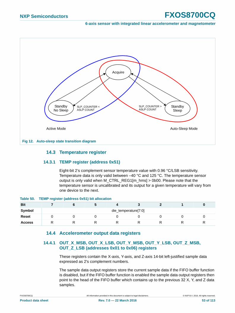
NXP Semiconductors FXOS8700CQ6-axis sensor with integrated linear accelerometer and magnetometer
14.3 Temperature register
14.3.1 TEMP register (address 0x51)
Eight-bit 2’s complement sensor temperature value with 0.96 °C/LSB sensitivity. Temperature data is only valid between –40 °C and 125 °C. The temperature sensor output is only valid when M_CTRL_REG1[m_hms] > 0b00. Please note that the temperature sensor is uncalibrated and its output for a given temperature will vary from one device to the next.
14.4 Accelerometer output data registers
14.4.1 OUT_X_MSB, OUT_X_LSB, OUT_Y_MSB, OUT_Y_LSB, OUT_Z_MSB, OUT_Z_LSB (addresses 0x01 to 0x06) registers
These registers contain the X-axis, Y-axis, and Z-axis 14-bit left-justified sample data expressed as 2's complement numbers.
The sample data output registers store the current sample data if the FIFO buffer function is disabled, but if the FIFO buffer function is enabled the sample data output registers then point to the head of the FIFO buffer which contains up to the previous 32 X, Y, and Z data samples.
Fig 12. Auto-sleep state transition diagram
Acquire
StandbyNo Sleep
StandbySleep
Active Mode Auto-Sleep Mode
SLP_COUNTER < SLP_COUNTER >ASLP COUNTASLP COUNT
Table 50. TEMP register (address 0x51) bit allocation
Bit 7 6 5 4 3 2 1 0
Symbol die_temperature[7:0]
Reset 0 0 0 0 0 0 0 0
Access R R R R R R R R
FXOS8700CQ All information provided in this document is subject to legal disclaimers. © NXP B.V. 2016. All rights reserved.
Product data sheet Rev. 7.0 — 22 March 2016 53 of 113
NXP Semiconductors FXOS8700CQ6-axis sensor with integrated linear accelerometer and magnetometer
The data is read out in the following order: Xmsb, Xlsb, Ymsb, Ylsb, Zmsb, Zlsb for CTRL_REG1[f_read] = 0, and Xmsb, Ymsb, Zmsb for CTRL_REG1[f_read] = 1. If the device is operating in hybrid mode and M_CTRL_REG2[hyb_autoinc_mode] = 1, The data read out order is acceleration Xmsb, Xlsb, Ymsb, Ylsb, Zmsb, and Zlsb followed by magnetic data Xmsb, Xlsb, Ymsb, Ylsb, Zmsb, Zlsb. Similarly, for CTRL_REG1[f_read] = 1, only the MSB's of the acceleration and magnetic data are read out in the same axis order.
If the CTRL_REG1[f_read] bit is set, auto-increment will skip over the LSB registers. This will shorten the data acquisition from six bytes to three bytes. If the LSB registers are directly addressed, the LSB information can still be read regardless of the CTRL_REG1[f_read] register setting.
If the FIFO data output register driver is enabled (F_SETUP[f_mode] > 0b00), register 0x01 points to the head of the FIFO buffer, while registers 0x02, 0x03, 0x04, 0x05, 0x06 return a value of zero when read directly.
The DR_STATUS registers, OUT_X_MSB, OUT_X_LSB, OUT_Y_MSB, OUT_Y_LSB, OUT_Z_MSB, and OUT_Z_LSB are located in the auto-incrementing address range of 0x00 to 0x06, allowing all of the acceleration data to be read in a single-burst read of six bytes starting at the OUT_X_MSB register. If the device is operating in hybrid mode and M_CTRL_REG2[hyb_autoinc_mode] = 1, the magnetometer data can also be read out in the same axis and endian order by executing a burst read of 12 bytes starting at register OUT_X_MSB.
Table 51. OUT_X_MSB register (address 0x01) bit allocation
Bit 7 6 5 4 3 2 1 0
Symbol xd[13:6]
Reset 0 0 0 0 0 0 0 0
Access R R R R R R R R
Table 52. OUT_X_LSB register (address 0x02) bit allocation
Bit 7 6 5 4 3 2 1 0
Symbol xd[5:0] - -
Reset 0 0 0 0 0 0 0 0
Access R R R R R R R R
Table 53. OUT_Y_MSB register (address 0x03) bit allocation
Bit 7 6 5 4 3 2 1 0
Symbol yd[13:6]
Reset 0 0 0 0 0 0 0 0
Access R R R R R R R R
Table 54. OUT_Y_LSB register (address 0x04) bit allocation
Bit 7 6 5 4 3 2 1 0
Symbol yd[5:0] - -
Reset 0 0 0 0 0 0 0 0
Access R R R R R R R R
FXOS8700CQ All information provided in this document is subject to legal disclaimers. © NXP B.V. 2016. All rights reserved.
Product data sheet Rev. 7.0 — 22 March 2016 54 of 113
NXP Semiconductors FXOS8700CQ6-axis sensor with integrated linear accelerometer and magnetometer
14.5 Accelerometer FIFO register
14.5.1 F_SETUP register (address 0x09)
[1] This bit field can be written in active mode.
[2] This bit field can be written in standby mode.
[3] The FIFO mode (f_mode) cannot be switched between operational modes (0b01, 0b10 and 0b11).
A FIFO sample count exceeding the watermark event does not stop the FIFO from accepting new data.
Table 55. OUT_Z_MSB register (address 0x05) bit allocation
Bit 7 6 5 4 3 2 1 0
Symbol zd[13:6]
Reset 0 0 0 0 0 0 0 0
Access R R R R R R R R
Table 56. OUT_Z_LSB register (address 0x06) bit allocation
Bit 7 6 5 4 3 2 1 0
Symbol zd[5:0] - -
Reset 0 0 0 0 0 0 0 0
Access R R R R R R R R
Table 57. F_SETUP register (address 0x09) bit allocation
Bit 7 6 5 4 3 2 1 0
Symbol f_mode[1:0] f_wmrk[5:0]
Reset 0 0 0 0 0 0 0 0
Access R/W R/W R/W R/W R/W R/W R/W R/W
Table 58. F_SETUP register (address 0x09) bit descriptions
Field Description
f_mode[1:0] [1][2][3]
FIFO buffer operating mode.
0b00 – FIFO is disabled.
0b01 – FIFO contains the most recent samples when overflowed (circular buffer). Oldest sample is discarded to be replaced by new sample.
0b10 – FIFO stops accepting new samples when overflowed.
0b11 – FIFO trigger mode.
The FIFO is flushed whenever the FIFO is disabled, during an automatic ODR change (auto-sleep/wake), or on a transition from standby mode to active mode.
Disabling the FIFO (f_mode = 0b00) resets the F_STATUS[f_ovf], F_STATUS[f_wmrk_flag], F_STATUS[f_cnt] status flags to zero.
A FIFO overflow event (that is, F_STATUS[f_cnt] = 32) will assert the F_STATUS[f_ovf] flag.
f_wmrk[5:0][2] FIFO sample count watermark.
These bits set the number of FIFO samples required to trigger a watermark interrupt. A FIFO watermark event flag F_STATUS[f_wmk_flag] is raised when FIFO sample count F_STATUS[f_cnt] value is equal to or greater than the f_ wmrk watermark.
Setting the f_wmrk to 0b00_0000 will disable the FIFO watermark event flag generation.
This field is also used to set the number of pre-trigger samples in trigger mode (f_mode = 0b11).
FXOS8700CQ All information provided in this document is subject to legal disclaimers. © NXP B.V. 2016. All rights reserved.
Product data sheet Rev. 7.0 — 22 March 2016 55 of 113
NXP Semiconductors FXOS8700CQ6-axis sensor with integrated linear accelerometer and magnetometer
The FIFO update rate is dictated by the selected system ODR. In active mode the ODR is set by CTRL_REG1[dr] and when auto-sleep is active, the ODR is set by CTRL_REG1[aslp_rate] bit fields.
When data is read from the FIFO buffer, the oldest sample data in the buffer is returned and also deleted from the front of the FIFO, while the FIFO sample count is decremented by one. It is assumed that the host application will use the I2C or SPI burst-read transactions to dump the FIFO contents. If the FIFO X, Y, and Z data is not completely read in one burst-read transaction, the next read will start at the next FIFO location X-axis data. If the Y or Z data is not read out in the same burst transaction as the X-axis data, it will be lost.
In trigger mode, the FIFO is operated as a circular buffer and will contain up to the 32 most recent acceleration data samples. The oldest sample is discarded and replaced by the current sample, until a FIFO trigger event occurs. After a trigger event occurs, the FIFO will continue to accept samples only until overflowed, after which point the newest sample data is discarded. For more information on using the FIFO buffer and the various FIFO operating modes, please refer to NXP application note AN4073.
14.6 Accelerometer sensor data configuration register
14.6.1 XYZ_DATA_CFG register (address 0x0E)
The XYZ_DATA_CFG register is used to configure the desired acceleration full-scale range, and also to select whether the output data is passed through the high-pass filter.
Table 59. XYZ_DATA_CFG register (address 0x0E) bit allocation
Bit 7 6 5 4 3 2 1 0
Symbol - - - hpf_out - - fs[1:0]
Reset 0 0 0 0 0 0 0 0
Access R/W R/W R/W R/W R/W R/W R/W R/W
Table 60. XYZ_DATA_CFG register (address 0x0E) bit descriptions
Field Description
hpf_out Enable high-pass filter on acceleration output data
1 – Output data is high-pass filtered
0 – High-pass filter is disabled.
fs[1:0] Accelerometer full-scale range selection. See Table 61.
Table 61. Full-scale range selection
fs[1] fs[0] Sensitivity Full-scale range
0 0 ±0.244 mg/LSB ±2 g
0 1 ±0.488 mg/LSB ±4 g
1 0 ±0.976 mg/LSB ±8 g
1 1 Reserved -
FXOS8700CQ All information provided in this document is subject to legal disclaimers. © NXP B.V. 2016. All rights reserved.
Product data sheet Rev. 7.0 — 22 March 2016 56 of 113
NXP Semiconductors FXOS8700CQ6-axis sensor with integrated linear accelerometer and magnetometer
14.7 Accelerometer high-pass filter register
14.7.1 HP_FILTER_CUTOFF register (address 0x0F)
High-pass filter cutoff frequency setting register.
Table 62. HP_FILTER_CUTOFF register (address 0x0F) bit allocation
Bit 7 6 5 4 3 2 1 0
Symbol - - pulse_hpf_byp pulse_lpf_en - - sel[1:0]
Reset 0 0 0 0 0 0 0 0
Access R/W R/W R/W R/W R/W R/W R/W R/W
Table 63. HP_FILTER_CUTOFF register (address 0x0F) bit descriptions
Field Description
pulse_hpf_byp Bypass high-pass filter for pulse processing function
0 – HPF enabled for pulse processing
1 – HPF bypassed for pulse processing
pulse_lpf_en Enable low-pass filter for pulse processing function
0 – LPF disabled for pulse processing
1 – LPF enabled for pulse processing
sel[1:0] HPF cutoff frequency selection
See Table 64.
Table 64. HP_FILTER_CUTOFF
High-Pass cutoff frequency (Hz)
ODR (Hz) sel = 0b00 sel = 0b01
Normal LPLN High resolution
Low power Normal LPLN High resolution
Low power
800 16 16 16 16 8 8 8 8
400 16 16 16 8 8 8 8 4
200 8 8 16 4 4 4 8 2
100 4 4 16 2 2 2 8 1
50 2 2 16 1 1 1 8 0.5
12.5 2 0.5 16 0.25 1 0.25 8 0.125
6.25 2 0.25 16 0.125 1 0.125 8 0.063
1.56 2 0.063 16 0.031 1 0.031 8 0.016
800 4 4 4 4 2 2 2 2
400 4 4 4 2 2 2 2 1
200 2 2 4 1 1 1 2 0.5
100 1 1 4 0.5 0.5 0.5 2 0.25
50 0.5 0.5 4 0.25 0.25 0.25 2 0.125
12.5 0.5 0.125 4 0.063 0.25 0.063 2 0.031
6.25 0.5 0.063 4 0.031 0.25 0.031 2 0.016
1.56 0.5 0.016 4 0.008 0.25 0.008 2 0.004
FXOS8700CQ All information provided in this document is subject to legal disclaimers. © NXP B.V. 2016. All rights reserved.
Product data sheet Rev. 7.0 — 22 March 2016 57 of 113
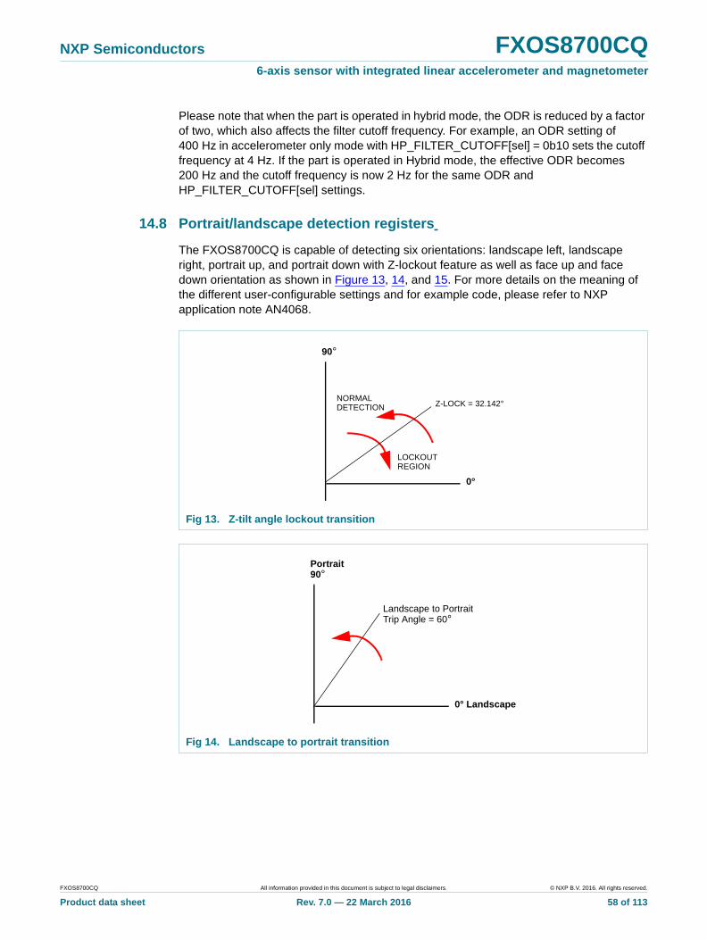
NXP Semiconductors FXOS8700CQ6-axis sensor with integrated linear accelerometer and magnetometer
Please note that when the part is operated in hybrid mode, the ODR is reduced by a factor of two, which also affects the filter cutoff frequency. For example, an ODR setting of 400 Hz in accelerometer only mode with HP_FILTER_CUTOFF[sel] = 0b10 sets the cutoff frequency at 4 Hz. If the part is operated in Hybrid mode, the effective ODR becomes 200 Hz and the cutoff frequency is now 2 Hz for the same ODR and HP_FILTER_CUTOFF[sel] settings.
14.8 Portrait/landscape detection registers
The FXOS8700CQ is capable of detecting six orientations: landscape left, landscape right, portrait up, and portrait down with Z-lockout feature as well as face up and face down orientation as shown in Figure 13, 14, and 15. For more details on the meaning of the different user-configurable settings and for example code, please refer to NXP application note AN4068.
Fig 13. Z-tilt angle lockout transition
Fig 14. Landscape to portrait transition
NORMAL
90°
Z-LOCK = 32.142°
0°
DETECTION
LOCKOUTREGION
Portrait
Landscape to Portrait
90°
Trip Angle = 60°
0° Landscape
FXOS8700CQ All information provided in this document is subject to legal disclaimers. © NXP B.V. 2016. All rights reserved.
Product data sheet Rev. 7.0 — 22 March 2016 58 of 113
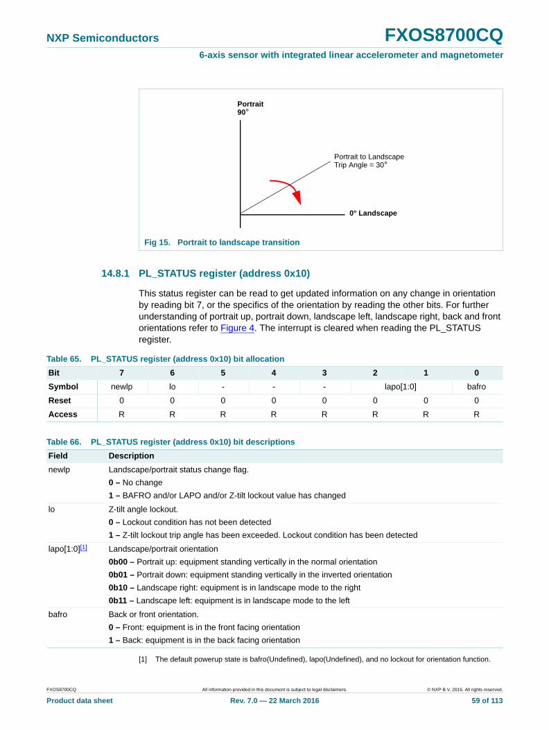
NXP Semiconductors FXOS8700CQ6-axis sensor with integrated linear accelerometer and magnetometer
.
.
14.8.1 PL_STATUS register (address 0x10)
This status register can be read to get updated information on any change in orientation by reading bit 7, or the specifics of the orientation by reading the other bits. For further understanding of portrait up, portrait down, landscape left, landscape right, back and front orientations refer to Figure 4. The interrupt is cleared when reading the PL_STATUS register.
[1] The default powerup state is bafro(Undefined), lapo(Undefined), and no lockout for orientation function.
Fig 15. Portrait to landscape transition
Portrait
Portrait to Landscape
90°
Trip Angle = 30°
0° Landscape
Table 65. PL_STATUS register (address 0x10) bit allocation
Bit 7 6 5 4 3 2 1 0
Symbol newlp lo - - - lapo[1:0] bafro
Reset 0 0 0 0 0 0 0 0
Access R R R R R R R R
Table 66. PL_STATUS register (address 0x10) bit descriptions
Field Description
newlp Landscape/portrait status change flag.
0 – No change
1 – BAFRO and/or LAPO and/or Z-tilt lockout value has changed
lo Z-tilt angle lockout.
0 – Lockout condition has not been detected
1 – Z-tilt lockout trip angle has been exceeded. Lockout condition has been detected
lapo[1:0][1] Landscape/portrait orientation
0b00 – Portrait up: equipment standing vertically in the normal orientation
0b01 – Portrait down: equipment standing vertically in the inverted orientation
0b10 – Landscape right: equipment is in landscape mode to the right
0b11 – Landscape left: equipment is in landscape mode to the left
bafro Back or front orientation.
0 – Front: equipment is in the front facing orientation
1 – Back: equipment is in the back facing orientation
FXOS8700CQ All information provided in this document is subject to legal disclaimers. © NXP B.V. 2016. All rights reserved.
Product data sheet Rev. 7.0 — 22 March 2016 59 of 113
NXP Semiconductors FXOS8700CQ6-axis sensor with integrated linear accelerometer and magnetometer
The newlp bit is set to 1 after the first orientation detection after a standby to active transition, and whenever a change in lo, bafro, or lapo occurs. The newlp bit is cleared anytime the PL_STATUS register is read. lapo, bafro and lo continue to change when newlp is set. The current orientation is locked if the absolute value of the acceleration experienced on any of the three axes is greater than 1.25 g.
14.8.2 PL_CFG register (address 0x11)
This register enables the portrait/landscape function and sets the behavior of the debounce counter.
14.8.3 PL_COUNT register (address 0x12)
This register sets the debounce count for the orientation state transition. The minimum debounce latency is determined by the system ODR value and the value of the PL_COUNT register. Any change to the system ODR or a transition from active-to-standby (or vice-versa) resets the internal landscape/portrait internal debounce counters. When the device is operated in hybrid mode, the effective ODR will be half of what is selected by the user, which will also affect the debounce time. For example, if an ODR of 400 Hz is selected and the part is also in hybrid mode, the effective ODR is 200 Hz, and the effective debounce time step is 5 ms instead of 2.5 ms.
Table 67. PL_CFG register (address 0x11) bit allocation
Bit 7 6 5 4 3 2 1 0
Symbol dbcntm pl_en - - - - - -
Reset 1 0 0 0 0 0 0 0
Access R/W R/W R/W R/W R/W R/W R/W R/W
Table 68. PL_CFG register (address 0x11) bit descriptions
Field Description
dbcntm Debounce counter mode selection.
0 – Decrements debounce whenever condition of interest is no longer valid.
1 – Clears counter whenever condition of interest is no longer valid
pl_en Portrait/landscape detection enable.
0 – Portrait/landscape detection is disabled.
1 – Portrait/landscape detection is enabled
Table 69. PL_COUNT register (address 0x12) bit allocation
Bit 7 6 5 4 3 2 1 0
Symbol dbnce[7:0]
Reset 0 0 0 0 0 0 0 0
Access R/W R/W R/W R/W R/W R/W R/W R/W
FXOS8700CQ All information provided in this document is subject to legal disclaimers. © NXP B.V. 2016. All rights reserved.
Product data sheet Rev. 7.0 — 22 March 2016 60 of 113
NXP Semiconductors FXOS8700CQ6-axis sensor with integrated linear accelerometer and magnetometer
14.8.4 PL_BF_ZCOMP register (address 0x13)
Back/front and Z-tilt angle compensation register.
Table 70. PL_Count Relationship with the ODR
ODR (Hz) Max time range (s) Time step (ms)
Normal LPLN High resolution
Low power Normal LPLN High resolution
Low power
800 0.319 0.319 0.319 0.319 1.25 1.25 1.25 1.25
400 0.638 0.638 0.638 0.638 2.5 2.5 2.5 2.5
200 1.28 1.28 0.638 1.28 5 5 2.5 5
100 2.55 2.55 0.638 2.55 10 10 2.5 10
50 5.1 5.1 0.638 5.1 20 20 2.5 20
12.5 5.1 20.4 0.638 20.4 20 80 2.5 80
6.25 5.1 20.4 0.638 40.8 20 80 2.5 160
1.56 5.1 20.4 0.638 40.8 20 80 2.5 160
Table 71. PL_BF_ZCOMP register (address 0x13) bit allocation
Bit 7 6 5 4 3 2 1 0
Symbol bkfr[1:0] - - - zlock[2:0]
Reset 1 0 0 0 0 1 0 0
Access R/W R/W R/W R/W R/W R/W R/W R/W
Table 72. PL_BF_ZCOMP register (address 0x13) bit descriptions
Field Description
zlock[2:0] Z-lock angle threshold. range is from approximately 13° to 44°. Step size is approximately 4°. See Table 73 for more information.
Default value: 0x04 → ∼28°
Maximum value: 0x07 → ~44°
bkfr[1:0] Back/front trip angle threshold. See Table 74 for more information.
Default: 0b10 → ±70°. Step size is 5°.
Range: ±(65° to 80°)
Table 73. Z-lockout angle definitions
zlock Resultant angle (min) for positionsbetween landscape and portrait
Resultant angle (max) for ideal landscape or portrait
0b000 13.6° 14.5°
0b001 17.1° 18.2°
0b010 20.7° 22.0°
0b011 24.4° 25.9°
0b100 28.1° 30.0°
0b101 32.0° 34.2°
0b110 36.1° 38.7°
0b111 40.4° 43.4°
FXOS8700CQ All information provided in this document is subject to legal disclaimers. © NXP B.V. 2016. All rights reserved.
Product data sheet Rev. 7.0 — 22 March 2016 61 of 113
NXP Semiconductors FXOS8700CQ6-axis sensor with integrated linear accelerometer and magnetometer
14.8.5 PL_THS_REG register (address 0x14)
Portrait to landscape trip threshold registers.
Table 74. Back/front orientation definitions
bkfr Back → front transition Front → back transition
0b00 Z < 80° or Z > 280° Z > 100° and Z < 260°
0b01 Z < 75° or Z > 285° Z > 105° and Z < 255°
0b10 Z < 70° or Z > 290° Z > 110° and Z < 250°
0b11 Z < 65° or Z > 295° Z > 115° and Z < 245°
Table 75. PL_THS_REG register (address 0x14) bit allocation
Bit 7 6 5 4 3 2 1 0
Symbol pl_ths[4:0] hys[2:0]
Reset 0 1 0 0 0 1 0 0
Access R/W R/W R/W R/W R/W R/W R/W R/W
Table 76. Threshold angle lookup table
pl_ths[4:0] value Threshold angle (approx.)
0x07 15°
0x09 20°
0x0C 30°
0x0D 35°
0x0F 40°
0x10 45°
0x13 55°
0x14 60°
0x17 70°
0x19 75°
Table 77. Trip angles versus hysteresis settings
hys[2:0] value Landscape to portrait trip angle Portrait to landscape trip angle
0b000 45° 45°
0b001 49° 41°
0b010 52° 38°
0b011 56° 34°
0b100 59° 31°
0b101 62° 28°
0b110 66° 24°
0b111 69° 21°
FXOS8700CQ All information provided in this document is subject to legal disclaimers. © NXP B.V. 2016. All rights reserved.
Product data sheet Rev. 7.0 — 22 March 2016 62 of 113
NXP Semiconductors FXOS8700CQ6-axis sensor with integrated linear accelerometer and magnetometer
14.9 Freefall and motion detection registers
The freefall/motion detection block can be configured to detect low-g (freefall) or high-g (motion) events utilizing the A_FFMT_CFG[a_ffmt_oae] bit.
In low-g detect mode (A_FFMT_CFG[a_ffmt_oae] = 0) a low-g condition will need to occur on all enabled axes (ex. X, Y and Z) for the A_FFMT_SRC[a_ffmt_ea] bit to be affected. And, in high-g detect mode (A_FFMT_CFG[a_ffmt_oae] = 1) a high-g condition occurring in any of the enabled axes (ex. X, Y or Z) will suffice to affect the A_FFMT_SRC[a_ffmt_ea] bit.
The detection threshold(s) are programed in register 0x17 (A_FFMT_THS) for common threshold operation, and 0x73-0x78 (A_FFMT_THS_X/Y/Z) for individual axis threshold operation.
A_FFMT_CFG[a_ffmt_ele] bit determines the behavior of A_FFMT_SRC[a_ffmt_ea] bit in response to the desired acceleration event (low-g/high-g). When A_FFMT_CFG[a_ffmt_ele] = 1, the freefall or motion event is latched and the A_FFMT_SRC[a_ffmt_ea] flag can only be cleared by reading the A_FFMT_SRC register. When A_FFMT_CFG[a_ffmt_ele] = 0, freefall or motion events are not latched, and the A_FFMT_SRC[a_ffmt_ea] bit reflects the real-time status of the event detection.
A_FFMT_THS[a_ffmt_dbcntm] bit determines the debounce filtering behavior of the logic which sets the A_FFMT_SRC[a_ffmt_ea] bit. See Table 17 for details.
It is possible to enable/disable each axis used in the freefall/motion detection function by configuring bits A_FFMT_CFG[a_ffmt_xefe], A_FFMT_CFG[a_ffmt_yefe], and A_FFMT_CFG[a_ffmt_zefe].
The freefall/motion detection function has the option to use a common 7-bit unsigned threshold for each of the X, Y, and Z axes, or individual unsigned 13-bit thresholds for each axis. When A_FFMT_THS_X_MSB[a_ffmt_ths_xyz_en] = 0, the 7-bit threshold value stored in register 0x17 is used as a common 7-bit threshold for the X, Y, and Z axes. When a_ffmt_ths_xyz_en = 1, each axis may be programmed with an individual 13-bit threshold (stored in the A_FFMT_X/Y/Z MSB and LSB registers).
14.9.1 A_FFMT_CFG register (address 0x15)
Freefall/motion configuration register.
Table 78. Portrait/landscape ideal orientation definitions
Position Description
PU y ~ –1 g, x ~ 0
PD y ~ +1 g, x ~ 0
LR y ~ 0, x ~ +1 g
LL y ~ 0, x ~ –1 g
Table 79. A_FFMT_CFG register (address 0x15) bit allocation
Bit 7 6 5 4 3 2 1 0
Symbol a_ffmt_ele a_ffmt_oae a_ffmt_zefe a_ffmt_yefe a_ffmt_xefe - - -
Reset 0 0 0 0 0 0 0 0
Access R/W R/W R/W R/W R/W R/W R/W R/W
FXOS8700CQ All information provided in this document is subject to legal disclaimers. © NXP B.V. 2016. All rights reserved.
Product data sheet Rev. 7.0 — 22 March 2016 63 of 113
NXP Semiconductors FXOS8700CQ6-axis sensor with integrated linear accelerometer and magnetometer
14.9.2 A_FFMT_SRC register (address 0x16)
Freefall/motion source register. Read-only register.
This register keeps track of the acceleration event which is triggering (or has triggered, in case of A_FFMT_CFG[a_ffmt_ele] = 1) the event flag. In particular A_FFMT_SRC[a_ffmt_ea] is set to a logic ‘1’ when the logical combination of acceleration event flags specified in A_FFMT_CFG register is true. This bit is used in combination with the values in CTRL_REG4[int_en_ffmt] and CTRL_REG5[int_cfg_ffmt] register bits to generate the freefall/motion interrupts.
Table 80. A_FFMT_CFG register (address 0x15) bit descriptions
Field Description
a_ffmt_ele a_ffmt_ele denotes whether the enabled event flag will be latched in the A_FFMT_SRC register or the event flag status in the A_FFMT_SRC will indicate the real-time status of the event. If a_ffmt_ele bit is set to a logic ‘1’, then the event flags are frozen when the a_ffmt_ea bit gets set, and are cleared by reading the A_FFMT_SRC source register.
0 – Event flag latch disabled
1 – Event flag latch enabled
a_ffmt_oae a_ffmt_oae bit allows the selection between motion (logical OR combination of high-g X, Y, and Z-axis event flags) and freefall (logical AND combination of low-g X, Y, and Z-axis event flags) detection.
Motion detect/freefall detect logic selection.
0 – Freefall flag (logical AND combination of low-g X, Y, and Z-axis event flags)
1 – Motion flag (logical OR combination of high-g X, Y, and Z-axis event flags)
a_ffmt_zefe a_ffmt_zefe enables the detection of a high- or low-g event when the measured acceleration data on Z-axis is above/below the threshold set in the A_FFMT_THS register. If the a_ffmt_ele bit is set to logic ‘1’ in the A_FFMT_CFG register, new event flags are blocked from updating the A_FFMT_SRC register.
0 – Event detection disabled
1 – Raise event flag on measured Z-axis acceleration above/below threshold.
a_ffmt_yefe a_ffmt_yefe enables the detection of a high- or low-g event when the measured acceleration data on Y-axis is above/below the threshold set in the A_FFMT_THS register. If the a_ffmt_ele bit is set to logic ‘1’ in the A_FFMT_CFG register, new event flags are blocked from updating the A_FFMT_SRC register.
0 – Event detection disabled
1 – Raise event flag on measured Y-axis acceleration above/below threshold.
a_ffmt_xefe a_ffmt_xefe enables the detection of a high- or low-g event when the measured acceleration data on X-axis is above/below the threshold set in the A_FFMT_THS register. If the a_ffmt_ele bit is set to logic ‘1’ in the A_FFMT_CFG register, new event flags are blocked from updating the A_FFMT_SRC register.
0 – Event detection disabled
1 – Raise event flag on measured X-axis acceleration above/below threshold.
Table 81. A_FFMT_SRC register (address 0x16) bit allocation
Bit 7 6 5 4 3 2 1 0
Symbol a_ffmt_ea - a_ffmt_zhe a_ffmt_zhp a_ffmt_yhe a_ffmt_yhp a_ffmt_xhe a_ffmt_xhp
Reset 0 0 0 0 0 0 0 0
Access R/W R/W R/W R/W R/W R/W R/W R/W
FXOS8700CQ All information provided in this document is subject to legal disclaimers. © NXP B.V. 2016. All rights reserved.
Product data sheet Rev. 7.0 — 22 March 2016 64 of 113
NXP Semiconductors FXOS8700CQ6-axis sensor with integrated linear accelerometer and magnetometer
14.9.3 A_FFMT_THS register (address 0x17)
Freefall/motion detection threshold registers.
Table 82. A_FFMT_SRC register (address 0x16) bit descriptions
Field Description
a_ffmt_ea Event active flag.
0 – No event flag has been asserted
1 – One or more event flag has been asserted. See Table 80 for the description of the A_FFMT_CFG[a_ffmt_oae] bit to determine the effect of the 3-axis event flags on the a_ffmt_ea bit.
a_ffmt_zhe Z-high event flag.
0 – Event detected
1 – Z-high event has been detected
This bit always reads zero if the a_ffmt_zefe control bit is set to zero
a_ffmt_zhp Z-high event polarity flag.
0 – Z event was positive g1 – Z event was negative gThis bit read always zero if the a_ffmt_zefe control bit is set to zero
a_ffmt_yhe Y-high event flag.
0 – No event detected
1 – Y-high event has been detected
This bit read always zero if the a_ffmt_yefe control bit is set to zero
a_ffmt_yhp Y-high event polarity flag.
0 – Y event detected was positive g1 – Y event was negative gThis bit always reads zero if the a_ffmt_yefe control bit is set to zero
a_ffmt_xhe X-high event flag.
0 – No event detected
1 – X-high event has been detected
This bit always reads zero if the a_ffmt_xefe control bit is set to zero
a_ffmt_xhp X-high event polarity flag.
0 – X event was positive g1 – X event was negative gThis bit always reads zero if the a_ffmt_xefe control bit is set to zero
Table 83. A_FFMT_THS register (address 0x17) bit allocation
Bit 7 6 5 4 3 2 1 0
Symbol a_ffmt_dbcntm ths[6:0]
Reset 0 0 0 0 0 0 0 0
Access R/W R/W R/W R/W R/W R/W R/W R/W
FXOS8700CQ All information provided in this document is subject to legal disclaimers. © NXP B.V. 2016. All rights reserved.
Product data sheet Rev. 7.0 — 22 March 2016 65 of 113
NXP Semiconductors FXOS8700CQ6-axis sensor with integrated linear accelerometer and magnetometer
14.9.4 A_FFMT_ THS_X_MSB, A_FFMT_THS_X_LSB, A_FFMT_THS_Y_MSB, A_FFMT_THS_Y_LSB, A_FFMT_THS_Z_MSB, A_FFMT_THS_Z_LSB registers (addresses 0x73 to 0x78)
Table 84. A_FFMT_THS register (address 0x17) bit descriptions
Field Description
a_ffmt_dbcntm The ASIC uses a_ffmt_dbcntm to set the acceleration FFMT debounce counter clear mode independent of the value of the a_ffmt_ths_xyz_en.
a_ffmt_dbcntm bit configures the way in which the debounce counter is reset when the inertial event of interest is momentarily not true.
When a_ffmt_dbcntm bit is a logic ‘1’, the debounce counter is cleared to 0 whenever the inertial event of interest is no longer true (part b, Table 17) while if the a_ffmt_dbcntm bit is set to logic ‘0’ the debounce counter is decremented by 1 whenever the inertial event of interest in longer true (part c, Table 17) until the debounce counter reaches 0 or the inertial event of interest become active.
The decrementing of the debounce counter acts to filter out irregular spurious events which might impede the correct detection of inertial events.
ths[6:0] Freefall/motion detection threshold: default value: 0b000_0000. Resolution is fixed at 63 mg/LSB.
Table 85. A_FFMT_THS_X_MSB register (address 0x73) bit allocation
Bit 7 6 5 4 3 2 1 0
Symbol a_ffmt_ths_xyz_en a_ffmt_ths_x[12:6]
Reset 0 0 0 0 0 0 0 0
Access R/W R/W R/W R/W R/W R/W R/W R/W
Table 86. A_FFMT_THS_X_MSB register (address 0x73) bit descriptions
Field Description
a_ffmt_ths_xyz_en For a_ffmt_ths_xyz_en = 0 the ASIC uses the ffmt_ths[6:0] value located in register 0x17[6:0] as a common threshold for the X, Y, and Z-axis acceleration detection. The common unsigned 7-bit acceleration threshold has a fixed resolution of 63 mg/LSB, with a range of 0 to 127 counts.
For a_ffmt_ths_xyz_en = 1 the ASIC ignores the common 7-bit G_FFMT_THS value located in register 0x17 when executing the FFMT function, and the following independent threshold values are used for each axis:
A_FFMT_THS_X_MSB and A_FFMT_THS_X_LSB are used for the X-axis acceleration threshold,
A_FFMT_THS_Y_MSB and A_FFMT_THS_Y_LSB for the Y-axis acceleration threshold, and
A_FFMT_THS_Z_MSB and A_FFMT_THS_Z_LSB for the Z-axis acceleration threshold.
The A_FFMT_THS_X/Y/Z thresholds are 13-bit unsigned values that has a fixed resolution of about 63 mg/LSB. The a_ffmt_ths_xyz_en and a_ffmt_trans_ths_en bits must not be enabled simultaneously.
a_ffmt_ths_x[12:6] 7-bit MSB of X-axis acceleration threshold.
Table 87. A_FFMT_THS_X_LSB register (address 0x74) bit allocation
Bit 7 6 5 4 3 2 1 0
Symbol a_ffmt_ths_x[5:0] - -
Reset 0 0 0 0 0 0 0 0
Access R/W R/W R/W R/W R/W R/W R/W R/W
FXOS8700CQ All information provided in this document is subject to legal disclaimers. © NXP B.V. 2016. All rights reserved.
Product data sheet Rev. 7.0 — 22 March 2016 66 of 113
NXP Semiconductors FXOS8700CQ6-axis sensor with integrated linear accelerometer and magnetometer
A_FFMT_THS contains the unsigned 7-bit threshold value used by the freefall/motion detection functional block and is used to detect either low-g (freefall) or high-g (motion) events depending on the setting of G_FFMT_CFG[f_ffmt_oae]. If g_ffmt_oae = 0, the event is detected when the absolute value of all the enabled axes are below the threshold value. When g_ffmt_oae = 1, the event is detected when the absolute value of any of the enabled axes is above the threshold value (see Figure 16 for an illustration of the freefall/motion event detection thresholds). If A_FFMT_THS_X_MSB[a_ffmt_ths_xyz_en] = 1, the behavior is identical, except that each axis may be programmed with an individual 13-bit threshold (stored in the A_FFMT_X/Y/Z MSB and LSB registers).
Table 88. A_FFMT_THS_Y_MSB register (address 0x75) bit allocation
Bit 7 6 5 4 3 2 1 0
Symbol a_ffmt_trans_ths_en
a_ffmt_ths_y[12:6]
Reset 0 0 0 0 0 0 0 0
Access R/W R/W R/W R/W R/W R/W R/W R/W
Table 89. A_FFMT_THS_Y_LSB register (address 0x76) bit allocation
Bit 7 6 5 4 3 2 1 0
Symbol a_ffmt_ths_y[5:0] - -
Reset 0 0 0 0 0 0 0 0
Access R/W R/W R/W R/W R/W R/W R/W R/W
Table 90. A_FFMT_THS_Y_MSB register (address 0x77) bit allocation
Bit 7 6 5 4 3 2 1 0
Symbol - a_ffmt_ths_z[12:6]
Reset 0 0 0 0 0 0 0 0
Access R/W R/W R/W R/W R/W R/W R/W R/W
Table 91. A_FFMT_THS_Z_LSB register (address 0x78) bit allocation
Bit 7 6 5 4 3 2 1 0
Symbol a_ffmt_ths_yz[5:0] - -
Reset 0 0 0 0 0 0 0 0
Access R/W R/W R/W R/W R/W R/W R/W R/W
Fig 16. A_FFMT_THS high and low-g level
+Full Scale
High-g Positive Threshold
Low-g Threshold
High-g Negative Threshold
-Full Scale
X, Y, Z High-g Region
X, Y, Z High-g Region
X, Y, Z Low-g Region
Negative
Positive
Acceleration
Acceleration(Motion OR of enabled axes)
(Freefall - AND of enabled axes)
(Motion - OR of enabled axes)
FXOS8700CQ All information provided in this document is subject to legal disclaimers. © NXP B.V. 2016. All rights reserved.
Product data sheet Rev. 7.0 — 22 March 2016 67 of 113
NXP Semiconductors FXOS8700CQ6-axis sensor with integrated linear accelerometer and magnetometer
14.9.5 A_FFMT_COUNT register (address 0x18)
Debounce count register for freefall/motion detection events
This register sets the number of debounce counts for acceleration sample data matching the user-programmed conditions for either a freefall or motion detection event required before the interrupt is triggered.
When the internal debounce counter reaches the A_FFMT_COUNT value a freefall/motion event flag is set. The debounce counter will never increase beyond the A_FFMT_COUNT value. The time step used for the debounce sample count depends on the ODR chosen (see Table 94). When the device is operated in hybrid mode, the effective ODR is half of what is selected in CTRL_REG1. This has the effect of doubling the time-step values shown in Table 94.
For example, an ODR of 100 Hz and a A_ FFMT_COUNT value of 15 would result in minimum debounce response time of 150 ms. If the device is operated in hybrid mode, the effective debounce response time will be 300 ms for the same settings.
Table 92. A_FFMT_COUNT register (address 0x18) bit allocation
Bit 7 6 5 4 3 2 1 0
Symbol a_ffmt_count[7:0]
Reset 0 0 0 0 0 0 0 0
Access R/W R/W R/W R/W R/W R/W R/W R/W
Table 93. A_FFMT_COUNT register (address 0x18) bit description
Field Description
a_ffmt_count[7:0] a_ffmt_count defines the minimum number of debounce sample counts required for the detection of a freefall or motion event. A_FFMT_THS[ffmt_dbcntm] determines the behavior of the counter when the condition of interest is momentarily not true.
Table 94. A_FFMT_COUNT relationship with the ODR
ODR (Hz) Max time range (s) Time step (ms)
Normal LPLN High resolution
Low power Normal LPLN High resolution
LP
800 0.319 0.319 0.319 0.319 1.25 1.25 1.25 1.25
400 0.638 0.638 0.638 0.638 2.5 2.5 2.5 2.5
200 1.28 1.28 0.638 1.28 5 5 2.5 5
100 2.55 2.55 0.638 2.55 10 10 2.5 10
50 5.1 5.1 0.638 5.1 20 20 2.5 20
12.5 5.1 20.4 0.638 20.4 20 80 2.5 80
6.25 5.1 20.4 0.638 40.8 20 80 2.5 160
1.56 5.1 20.4 0.638 40.8 20 80 2.5 160
FXOS8700CQ All information provided in this document is subject to legal disclaimers. © NXP B.V. 2016. All rights reserved.
Product data sheet Rev. 7.0 — 22 March 2016 68 of 113
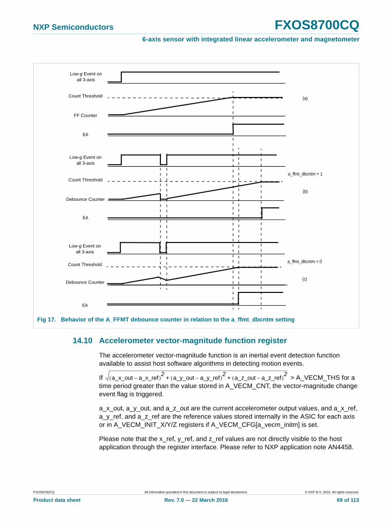
NXP Semiconductors FXOS8700CQ6-axis sensor with integrated linear accelerometer and magnetometer
14.10 Accelerometer vector-magnitude function register
The accelerometer vector-magnitude function is an inertial event detection function available to assist host software algorithms in detecting motion events.
If > A_VECM_THS for a time period greater than the value stored in A_VECM_CNT, the vector-magnitude change event flag is triggered.
a_x_out, a_y_out, and a_z_out are the current accelerometer output values, and a_x_ref, a_y_ref, and a_z_ref are the reference values stored internally in the ASIC for each axis or in A_VECM_INIT_X/Y/Z registers if A_VECM_CFG[a_vecm_initm] is set.
Please note that the x_ref, y_ref, and z_ref values are not directly visible to the host application through the register interface. Please refer to NXP application note AN4458.
Fig 17. Behavior of the A_FFMT debounce counter in relation to the a_ffmt_dbcntm setting
Low-g Event on
Count Threshold
EA
all 3-axis
FF Counter
Low-g Event on
Count Threshold
(a)
all 3-axis
Debounce Counter
Low-g Event on
Count Threshold
EA
all 3-axis
a_ffmt_dbcntm = 1
(b)
EA
a_ffmt_dbcntm = 0
(c)Debounce Counter
a_x_out a_x_ref–( )2 a_y_out a_y_ref–( )2 a_z_out a_z_ref–( )2+ +
FXOS8700CQ All information provided in this document is subject to legal disclaimers. © NXP B.V. 2016. All rights reserved.
Product data sheet Rev. 7.0 — 22 March 2016 69 of 113
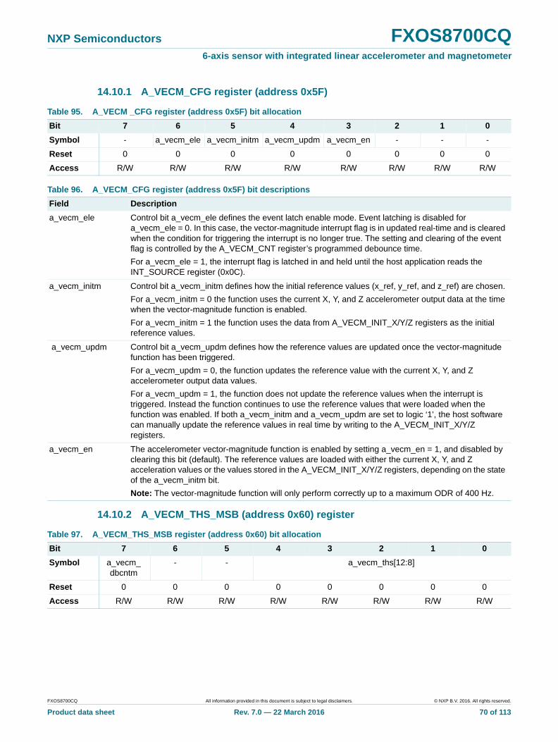
NXP Semiconductors FXOS8700CQ6-axis sensor with integrated linear accelerometer and magnetometer
14.10.1 A_VECM_CFG register (address 0x5F)
14.10.2 A_VECM_THS_MSB (address 0x60) register
Table 95. A_VECM _CFG register (address 0x5F) bit allocation
Bit 7 6 5 4 3 2 1 0
Symbol - a_vecm_ele a_vecm_initm a_vecm_updm a_vecm_en - - -
Reset 0 0 0 0 0 0 0 0
Access R/W R/W R/W R/W R/W R/W R/W R/W
Table 96. A_VECM_CFG register (address 0x5F) bit descriptions
Field Description
a_vecm_ele Control bit a_vecm_ele defines the event latch enable mode. Event latching is disabled for a_vecm_ele = 0. In this case, the vector-magnitude interrupt flag is in updated real-time and is cleared when the condition for triggering the interrupt is no longer true. The setting and clearing of the event flag is controlled by the A_VECM_CNT register’s programmed debounce time.
For a_vecm_ele = 1, the interrupt flag is latched in and held until the host application reads the INT_SOURCE register (0x0C).
a_vecm_initm Control bit a_vecm_initm defines how the initial reference values (x_ref, y_ref, and z_ref) are chosen.
For a_vecm_initm = 0 the function uses the current X, Y, and Z accelerometer output data at the time when the vector-magnitude function is enabled.
For a_vecm_initm = 1 the function uses the data from A_VECM_INIT_X/Y/Z registers as the initial reference values.
a_vecm_updm Control bit a_vecm_updm defines how the reference values are updated once the vector-magnitude function has been triggered.
For a_vecm_updm = 0, the function updates the reference value with the current X, Y, and Z accelerometer output data values.
For a_vecm_updm = 1, the function does not update the reference values when the interrupt is triggered. Instead the function continues to use the reference values that were loaded when the function was enabled. If both a_vecm_initm and a_vecm_updm are set to logic ‘1’, the host software can manually update the reference values in real time by writing to the A_VECM_INIT_X/Y/Z registers.
a_vecm_en The accelerometer vector-magnitude function is enabled by setting a_vecm_en = 1, and disabled by clearing this bit (default). The reference values are loaded with either the current X, Y, and Z acceleration values or the values stored in the A_VECM_INIT_X/Y/Z registers, depending on the state of the a_vecm_initm bit.
Note: The vector-magnitude function will only perform correctly up to a maximum ODR of 400 Hz.
Table 97. A_VECM_THS_MSB register (address 0x60) bit allocation
Bit 7 6 5 4 3 2 1 0
Symbol a_vecm_dbcntm
- - a_vecm_ths[12:8]
Reset 0 0 0 0 0 0 0 0
Access R/W R/W R/W R/W R/W R/W R/W R/W
FXOS8700CQ All information provided in this document is subject to legal disclaimers. © NXP B.V. 2016. All rights reserved.
Product data sheet Rev. 7.0 — 22 March 2016 70 of 113
NXP Semiconductors FXOS8700CQ6-axis sensor with integrated linear accelerometer and magnetometer
14.10.3 A_VECM_THS_LSB register (address 0x61)
14.10.4 A_VECM_CNT register (address 0x62)
The debounce timer period is determined by the ODR selected in CTRL_REG1; it is equal to the number indicated in A_VECM_CNT register times 1/ODR. For example, a value of 16 in A_VECM_CNT with an ODR setting of 400 Hz will result in a debounce period of 40 ms. Note that ODR is halved when in hybrid mode.
14.10.5 A_VECM_INITX_MSB register (address 0x63)
Table 98. A_VECM_THS_MSB register (address 0x60) bit descriptions
Field Description
a_vecm_dbcntm Control bit a_vecm_dbcntm defines how the debounce timer is reset when the condition for triggering the interrupt is no longer true.
When a_vecm_dbcntm = 0 the debounce counter is decremented by 1 when the vector-magnitude result is below the programmed threshold value.
When a_vecm_dbcntm = 1 the debounce counter is cleared when the vector-magnitude result is below the programmed threshold value.
a_vecm_ths[12:8] Five MSBs of the 13-bit unsigned A_VECM_THS value. The resolution is equal to the selected accelerometer resolution set in XYZ_DATA_CFG[fs]
Table 99. A_VECM_THS_LSB register (address 0x61) bit allocation
Bit 7 6 5 4 3 2 1 0
Symbol a_vecm_ths[7:0]
Reset 0 0 0 0 0 0 0 0
Access R/W R/W R/W R/W R/W R/W R/W R/W
Table 100. A_VECM_CNT register (address 0x62) bit allocation
Bit 7 6 5 4 3 2 1 0
Symbol a_vecm_cnt[7:0]
Reset 0 0 0 0 0 0 0 0
Access R/W R/W R/W R/W R/W R/W R/W R/W
Table 101. A_VECM_CNT register (address 0x62) bit description
Field Description
a_vecm_cnt[7:0] Vector-magnitude function debounce count value.
Table 102. A_VECM_INITX_MSB register (address 0x63) bit allocation
Bit 7 6 5 4 3 2 1 0
Symbol - - a_vecm_initx [13:8]
Reset 0 0 0 0 0 0 0 0
Access R/W R/W R/W R/W R/W R/W R/W R/W
Table 103. A_VECM_INITX_MSB register (address 0x63) bit description
Field Description
a_vecm_initx[13:8] Most significant 6 bits of the signed 14-bit initial X-axis value to be used as ref_x when A_VECM_CFG[a_vecm_initm] = 1. The resolution is determined by the settings made in XYZ_DATA_CFG[fs], and is equal to the accelerometer resolution.
FXOS8700CQ All information provided in this document is subject to legal disclaimers. © NXP B.V. 2016. All rights reserved.
Product data sheet Rev. 7.0 — 22 March 2016 71 of 113
NXP Semiconductors FXOS8700CQ6-axis sensor with integrated linear accelerometer and magnetometer
14.10.6 A_VECM_INITX_LSB register (address 0x64)
14.10.7 A_VECM_INITY_MSB register (address 0x65)
14.10.8 A_VECM_INITY_LSB register (address 0x66)
14.10.9 A_VECM_INITZ_MSB register (address 0x67)
Table 104. A_VECM_INITX_LSB register (address 0x64)
Bit 7 6 5 4 3 2 1 0
Symbol a_vecm_initx[7:0]
Reset 0 0 0 0 0 0 0 0
Access R/W R/W R/W R/W R/W R/W R/W R/W
Table 105. A_VECM_INITX_LSB register (address 0x64) bit description
Field Description
a_vecm_initx[7:0] LSB of the signed 14-bit initial X-axis value to be used as ref_x when A_VECM_CFG[a_vecm_initm] = 1. The resolution is determined by the settings made in XYZ_DATA_CFG[fs], and is equal to the accelerometer resolution.
Table 106. A_VECM_INITY_MSB register (address 0x65) bit allocation
Bit 7 6 5 4 3 2 1 0
Symbol - - a_vecm_inity
Reset 0 0 0 0 0 0 0 0
Access R/W R/W R/W R/W R/W R/W R/W R/W
Table 107. A_VECM_INITY_MSB register (address 0x65) bit description
Field Description
a_vecm_inity[13:8] Most significant 6 bits of the signed 14-bit initial Y-axis value to be used as ref_y when A_VECM_CFG[a_vecm_initm] = 1. The resolution is determined by the settings made in XYZ_DATA_CFG[fs], and is equal to the accelerometer resolution.
Table 108. A_VECM_INITY_LSB register (address 0x66) bit allocation
Bit 7 6 5 4 3 2 1 0
Symbol a_vecm_inity[7:0]
Reset 0 0 0 0 0 0 0 0
Access R/W R/W R/W R/W R/W R/W R/W R/W
Table 109. A_VECM_INITY_LSB register (address 0x66) bit description
Field Description
a_vecm_inity[7:0] LSB of the signed 14-bit initial Y-axis value to be used as ref_y when A_VECM_CFG[a_vecm_initm] = 1. The resolution is determined by the settings made in XYZ_DATA_CFG[fs], and is equal to the accelerometer resolution.
Table 110. A_VECM_INITZ_MSB register (address 0x67) bit allocation
Bit 7 6 5 4 3 2 1 0
Symbol - - a_vecm_initz[13:8]
Reset 0 0 0 0 0 0 0 0
Access R/W R/W R/W R/W R/W R/W R/W R/W
FXOS8700CQ All information provided in this document is subject to legal disclaimers. © NXP B.V. 2016. All rights reserved.
Product data sheet Rev. 7.0 — 22 March 2016 72 of 113
NXP Semiconductors FXOS8700CQ6-axis sensor with integrated linear accelerometer and magnetometer
14.10.10 A_VECM_INITZ_LSB register (address 0x68)
14.11 Transient (AC) acceleration detection registers
The transient detection function is similar to the freefall/motion detection function with the exception that a high-pass filter can be used to eliminate the DC offset from the acceleration data. There is an option to disable the high-pass filter, which causes the transient detection function to work in a similar manner to the motion detection function.
The transient detection function can be configured to signal an interrupt when the high-pass filtered acceleration delta values for any of the enabled axes exceeds the threshold programmed in TRANSIENT_THS for the debounce time programmed in TRANSIENT_COUNT. For more information on how to use and configure the transient detection function, refer to NXP application note AN4461.
Table 111. A_VECM_INITZ_MSB register (address 0x67) bit description
Field Description
a_vecm_initz[13:8] Most significant 6 bits of the signed 14-bit initial Z-axis value to be used as ref_z when A_VECM_CFG[a_vecm_initm] = 1. The resolution is determined by the settings made in XYZ_DATA_CFG[fs], and is equal to the accelerometer resolution.
Table 112. A_VECM_INITZ_LSB register (address 0x68) bit allocation
Bit 7 6 5 4 3 2 1 0
Symbol a_vecm_initz[7:0]
Reset 0 0 0 0 0 0 0 0
Access R/W R/W R/W R/W R/W R/W R/W R/W
Table 113. A_VECM_INITZ_LSB register (address 0x68) bit description
Field Description
a_vecm_initz[7:0] LSB of the signed 14-bit initial Z-axis value to be used as ref_z when A_VECM_CFG[a_vecm_initm] = 1. The resolution is determined by the settings made in XYZ_DATA_CFG[fs], and is equal to the accelerometer resolution.
FXOS8700CQ All information provided in this document is subject to legal disclaimers. © NXP B.V. 2016. All rights reserved.
Product data sheet Rev. 7.0 — 22 March 2016 73 of 113
NXP Semiconductors FXOS8700CQ6-axis sensor with integrated linear accelerometer and magnetometer
14.11.1 TRANSIENT_CFG register (address 0x1D)
14.11.2 TRANSIENT_SRC register (address 0x1E)
Transient event flag source register. This register provides the event status of the enabled axes and polarity (directional) information.
Table 114. TRANSIENT_ CFG register (address 0x1D) bit allocation
Bit 7 6 5 4 3 2 1 0
Symbol - - - tran_ele tran_zefe tran_yefe tran_xefe tran_hpf_byp
Reset 0 0 0 0 0 0 0 0
Access R/W R/W R/W R/W R/W R/W R/W R/W
Table 115. TRANSIENT_ CFG register (address 0x1D) bit descriptions
Field Description
tran_ele Transient event flag latch enable.
0 – Event flag latch disabled: the transient interrupt flag reflects the real-time status of the function.
1 – Event flag latch enabled: the transient interrupt event flag is latched and a read of the TRANSIENT_SRC register is required to clear the event flag.
tran_zefe Z-axis transient event flag enable.
0 – Z-axis event detection disabled
1 – Z-axis event detection enabled. Raise event flag on Z-axis acceleration value greater than threshold.
tran_yefe Y-axis transient event flag enable.
0 – Y-axis event detection disabled
1 – Y-axis event detection enabled. Raise event flag on Y-axis acceleration value greater than threshold.
tran_xefe X-axis transient event flag enable.
0 – X-axis event detection disabled
1 – X-axis event detection enabled. Raise event flag on X-axis acceleration value greater than threshold.
tran_hpf_byp Transient function high-pass filter bypass.
0 – High-pass filter is applied to accelerometer data input to the transient function.
1 – High-pass filter is not applied to accelerometer data input to the transient function.
Table 116. TRANSIENT_SRC register (address 0x1E) bit allocation
Bit 7 6 5 4 3 2 1 0
Symbol - tran_ea tran_zef tran_zpol tran_yef tran_ypol tran_xef trans_xpol
Reset 0 0 0 0 0 0 0 0
Access R R R R R R R R
FXOS8700CQ All information provided in this document is subject to legal disclaimers. © NXP B.V. 2016. All rights reserved.
Product data sheet Rev. 7.0 — 22 March 2016 74 of 113
NXP Semiconductors FXOS8700CQ6-axis sensor with integrated linear accelerometer and magnetometer
When TRANSIENT_CFG[tran_ele] = 1, the TRANSIENT_SRC event flag(s) and polarity bits are latched when the interrupt event is triggered, allowing the host application to determine which event flag(s) originally triggered the interrupt. When TRANSIENT_CFG[tran_ele] = 0, events which occur after the event that originally triggered the interrupt will update the flag and polarity bits, but once set, the flags can only be cleared by reading the TRANSIENT_SRC register.
14.11.3 TRANSIENT_THS register (address 0x1F)
The TRANSIENT_THS register determines the debounce counter behavior and also sets the transient event detection threshold.It is possible to use A_FFMT_THS_X/Y/Z MSB and LSB registers to set transient acceleration thresholds for individual axes using the a_ffmt_trans_ths_en bit in A_FFMT_THS_Y_MSB register. For a_ffmt_trans_ths_en = 1, register 0x1F[6:0] is used as the 7-bit, X-axis transient threshold, registers 0x75[0] and 0x76[7:2] as the 7-bit, Y-axis threshold and registers 0x77[0] and 0x78[7:2] as the 7-bit, Z-axis threshold.
Table 117. TRANSIENT_SRC register (address 0x1E) bit descriptions
Field Description
tran_ea Transient event active flag.
0 – No transient event active flag has been asserted.
1 – One or more transient event active flags has been asserted.
tran_zef Z-axis transient event active flag.
0 – Z-axis event flag is not active.
1 – Z-axis event flag is active; Z-axis acceleration has exceeded the programmed threshold for the debounce time specified in TRANS_COUNT.
tran_zpol Z-axis event flag polarity.
0 – Z-axis event was above positive threshold value.
1 – Z-axis event was below negative threshold value.
tran_yef Y-axis transient event active flag.
0 – Y-axis event flag is not active.
1 – Y-axis event flag is active; Y-axis acceleration has exceeded the programmed threshold for the debounce time specified in TRANS_COUNT.
tran_ypol Y-axis event flag polarity.
0 – Y-axis event was above positive threshold value.
1 – Y-axis event was below negative threshold value.
tran_xef X-axis transient event active flag.
0 – X-axis event flag is not active.
1 – X-axis event flag is active; X-axis acceleration has exceeded the programmed threshold for the debounce time specified in TRANS_COUNT.
tran_xpol X-axis event flag polarity.
0 – X-axis event was above positive threshold value.
1 – X-axis event was below negative threshold value.
FXOS8700CQ All information provided in this document is subject to legal disclaimers. © NXP B.V. 2016. All rights reserved.
Product data sheet Rev. 7.0 — 22 March 2016 75 of 113
NXP Semiconductors FXOS8700CQ6-axis sensor with integrated linear accelerometer and magnetometer
The tr_ths[6:0] value is a 7-bit unsigned number, with a fixed resolution of 63 mg/LSB corresponding to a ±8 g measurement range. The resolution does not change with the full-scale range setting made in XYZ_DATA_CFG[fs]. If CTRL_REG1[lnoise] = 1, the measurement range is fixed at ±4 g, regardless of the settings made in XYZ_DATA_CFG.
14.11.4 TRANSIENT_COUNT register (address 0x20)
The TRANSIENT_COUNT register sets the minimum number of debounce counts needed to trigger the transient event interrupt flag when the measured acceleration value exceeds the threshold set in TRANSIENT_THS for any of the enabled axes.
The time step for the transient detection debounce counter is set by the value of the system ODR and power mode as shown in Table 122. When the device is operated in hybrid mode, the effective ODR is half of what is selected in CTRL_REG1, which also doubles the time-step values shown in Table 122.
Table 118. TRANSIENT_THS register (address 0x1F) bit allocation
Bit 7 6 5 4 3 2 1 0
Symbol tr_dbcntm tr_ths[6:0]
Reset 0 0 0 0 0 0 0 0
Access R/W R/W R/W R/W R/W R/W R/W R/W
Table 119. TRANSIENT_THS register (address 0x1F) descriptions
Field Description
tr_dbcntm Debounce counter mode selection.
0 – Decrements debounce counter when the transient event condition is not true during the current ODR period.
1 – Clears debounce counter when the transient event condition is not true during the current ODR period.
tr_ths[6:0] Transient event threshold. This register has a resolution of 63 mg/LSB regardless of the full-scale range setting made in XYZ_DATA_CFG[fs]. If CTRL_REG1[lnoise] = 1, the maximum acceleration measurement range is ±4 g.
Table 120. TRANSIENT_COUNT register (address 0x20) bit allocation
Bit 7 6 5 4 3 2 1 0
Symbol tr_count[7:0]
Reset 0 0 0 0 0 0 0 0
Access R/W R/W R/W R/W R/W R/W R/W R/W
Table 121. TRANSIENT_COUNT register (address 0x20) bit description
Field Description
tr_count[7:0) Transient function debounce count value.
Table 122. TRANSIENT_COUNT relationship with the ODR
ODR (Hz) Max time range (s) Time step (ms)
Normal LPLN High resolution
Low power Normal LPLN High resolution
LP
800 0.319 0.319 0.319 0.319 1.25 1.25 1.25 1.25
400 0.638 0.638 0.638 0.638 2.5 2.5 2.5 2.5
200 1.28 1.28 0.638 1.28 5 5 2.5 5
FXOS8700CQ All information provided in this document is subject to legal disclaimers. © NXP B.V. 2016. All rights reserved.
Product data sheet Rev. 7.0 — 22 March 2016 76 of 113
NXP Semiconductors FXOS8700CQ6-axis sensor with integrated linear accelerometer and magnetometer
An ODR of 100 Hz and a TRANSIENT_COUNT value of 15, when accelerometer OSR is set to normal using CTRL_REG2, would result in minimum debounce response time of 150 ms. When the device is operated in hybrid mode, these settings would result in an effective debounce time of 300 ms.
14.12 Pulse detection registers
14.12.1 PULSE_CFG register (address 0x21)
This register configures the pulse event detection function.
100 2.55 2.55 0.638 2.55 10 10 2.5 10
50 5.1 5.1 0.638 5.1 20 20 2.5 20
12.5 5.1 20.4 0.638 20.4 20 80 2.5 80
6.25 5.1 20.4 0.638 40.8 20 80 2.5 160
1.56 5.1 20.4 0.638 40.8 20 80 2.5 160
Table 122. TRANSIENT_COUNT relationship with the ODR - ¶continued
ODR (Hz) Max time range (s) Time step (ms)
Normal LPLN High resolution
Low power Normal LPLN High resolution
LP
Table 123. PULSE_CFG register (address 0x21) bit allocation
Bit 7 6 5 4 3 2 1 0
Symbol pls_dpa pls_ele pls_zdpefe pls_zspefe pls_ydpefe pls_yspefe pls_xdpefe pls_xspefe
Reset 0 0 0 0 0 0 0 0
Access R/W R/W R/W R/W R/W R/W R/W R/W
Table 124. PULSE_CFG register (address 0x21) bit descriptions
Field Description
pls_dpa Double-pulse abort.
0 – Double-pulse detection is not aborted if the start of a pulse is detected during the time period specified by the PULSE_LTCY register.
1 – Setting the pls_dpa bit momentarily suspends the double-tap detection if the start of a pulse is detected during the time period specified by the PULSE_LTCY register and the pulse ends before the end of the time period specified by the PULSE_LTCY register.
pls_ele Pulse event flag latch enable. When enabled, a read of the PULSE_SRC register is needed to clear the event flag.
0 – Event flag latch disabled
1 – Event flag latch enabled
pls_zdpefe Event flag enable on double-pulse event on Z-axis.
0 – Event detection disabled
1 – Raise event flag on detection of double-pulse event on Z-axis
pls_zspefe Event flag enable on single-pulse event on Z-axis.
0 – Event detection disabled
1 – Raise event flag on detection of single-pulse event on Z-axis
pls_ydpefe Event flag enable on double-pulse event on Y-axis.
0 – Event detection disabled
1 – Raise event flag on detection of double-pulse event on Y-axis
FXOS8700CQ All information provided in this document is subject to legal disclaimers. © NXP B.V. 2016. All rights reserved.
Product data sheet Rev. 7.0 — 22 March 2016 77 of 113
NXP Semiconductors FXOS8700CQ6-axis sensor with integrated linear accelerometer and magnetometer
14.12.2 PULSE_SRC register (address 0x22)
This register indicates the status bits for the pulse detection function.
pls_yspefe Event flag enable on single-pulse event on Y-axis.
0 – Event detection disabled
1 – Raise event flag on detection of single-pulse event on Z-axis.
pls_xdpefe Event flag enable on double-pulse event on X-axis.
0 – Event detection disabled
1 – Raise event flag on detection of double-pulse event on X-axis.
pls_xspefe Event flag enable on single-pulse event on X-axis.
0 – Event detection disabled
1 – Raise event flag on detection of single-pulse event on X-axis.
Table 124. PULSE_CFG register (address 0x21) bit descriptions - ¶continued
Field Description
Table 125. PULSE_SRC register (address 0x22) bit allocation
Bit 7 6 5 4 3 2 1 0
Symbol pls_src_ea pls_src_axz pls_src_axy pls_src_axx pls_src_dpe pls_src_polz pls_src_poly pls_src_polx
Reset 0 0 0 0 0 0 0 0
Access R R R R R R R R
Table 126. PULSE_SRC register (address 0x22) bit descriptions
Field Description
pls_src_ea Event active flag.
0 – No interrupt has been generated
1 – One or more interrupt events have been generated
pls_src_axz Z-axis event flag.
0 – No interrupt
1 – Z-axis event has occurred
pls_src_axy Y-axis event flag.
0 – No interrupt
1 – Y-axis event has occurred
pls_src_axx X-axis event flag.
0 – No interrupt
1 – X-axis event has occurred.
pls_src_dpe Double pulse on first event.
0 – Single-pulse event triggered interrupt
1 – Double-pulse event triggered interrupt
FXOS8700CQ All information provided in this document is subject to legal disclaimers. © NXP B.V. 2016. All rights reserved.
Product data sheet Rev. 7.0 — 22 March 2016 78 of 113
NXP Semiconductors FXOS8700CQ6-axis sensor with integrated linear accelerometer and magnetometer
14.12.3 PULSE_THSX register (address 0x23)
The PULSE_THSX, PULSE_THSY and PULSE_THSZ registers define the thresholds used by the system to start the pulse-event detection procedure. Threshold values for each axis are unsigned 7-bit numbers with a fixed resolution of 0.063 g/LSB, corresponding to an 8 g acceleration full-scale range. The full-scale range is fixed at 8 g for the pulse detection function, regardless of the settings made in XYZ_DATA_CFG[fs].
14.12.4 PULSE_THSY register (address 0x24)
pls_src_polz Pulse polarity of Z-axis event.
0 – Pulse event that triggered interrupt was positive.
1 – Pulse event that triggered interrupt was negative.
pls_src_poly Pulse polarity of Y-axis event.
0 – Pulse event that triggered interrupt was positive.
1 – Pulse event that triggered interrupt was negative.
pls_src_polx Pulse polarity of X-axis event.
0 – Pulse event that triggered interrupt was positive.
1 – Pulse event that triggered interrupt was negative.
Table 126. PULSE_SRC register (address 0x22) bit descriptions - ¶continued
Field Description
Table 127. PULSE_THSX register (address 0x23) bit allocation
Bit 7 6 5 4 3 2 1 0
Symbol - pls_thsx[6:0]
Reset 0 0 0 0 0 0 0 0
Access R/W R/W R/W R/W R/W R/W R/W R/W
Table 128. PULSE_THSX register (address 0x23) bit description
Field Description
pls_thsx[6:0] Pulse threshold for X-axis.
Table 129. PULSE_THSY register (address 0x24) bit allocation
Bit 7 6 5 4 3 2 1 0
Symbol - pls_thsy[6:0]
Reset 0 0 0 0 0 0 0 0
Access R/W R/W R/W R/W R/W R/W R/W R/W
Table 130. PULSE_THSY register (address 0x24) bit description
Field Description
pls_thsy[6:0] Pulse threshold for Y-axis.
FXOS8700CQ All information provided in this document is subject to legal disclaimers. © NXP B.V. 2016. All rights reserved.
Product data sheet Rev. 7.0 — 22 March 2016 79 of 113
NXP Semiconductors FXOS8700CQ6-axis sensor with integrated linear accelerometer and magnetometer
14.12.5 PULSE_THSZ register (address 0x25)
14.12.6 PULSE_TMLT register (address 0x26)
Minimum time step for the pulse-time limit is defined in Table 135 and Table 136. Maximum time for a given ODR is “Minimum time step x 255”.
Table 131. PULSE_THSZ register (address 0x25) bit allocation
Bit 7 6 5 4 3 2 1 0
Symbol - pls_thsz[6:0]
Reset 0 0 0 0 0 0 0 0
Access R/W R/W R/W R/W R/W R/W R/W R/W
Table 132. PULSE_THSZ register (address 0x24) bit description
Field Description
pls_thsz[6:0] Pulse threshold for Z-axis.
Table 133. PULSE_TMLT register (address 0x26) bit allocation
Bit 7 6 5 4 3 2 1 0
Symbol pls_tmlt[7:0]
Reset 0 0 0 0 0 0 0 0
Access R/W R/W R/W R/W R/W R/W R/W R/W
Table 134. PULSE_TMLT register (address 0x26) bit description
Field Description
pls_tmlt[7:0] pls_tmlt[7:0] defines the maximum time interval that can elapse between the start of the acceleration on the selected channel exceeding the specified threshold and the end when the channel acceleration goes back below the specified threshold.
Table 135. Time step for PULSE_TMLT with HP_FILTER_CUTOFF[pls_hpf_en] = 1
ODR (Hz) Max time range (s) Time step (ms)
Normal LPLN High resolution
Low power Normal LPLN High resolution
LP
800 0.319 0.319 0.319 0.319 1.25 1.25 1.25 1.25
400 0.638 0.638 0.638 0.638 2.5 2.5 2.5 2.5
200 1.28 1.28 0.638 1.28 5 5 2.5 5
100 2.55 2.55 0.638 2.55 10 10 2.5 10
50 5.1 5.1 0.638 5.1 20 20 2.5 20
12.5 5.1 20.4 0.638 20.4 20 80 2.5 80
6.25 5.1 20.4 0.638 40.8 20 80 2.5 160
1.56 5.1 20.4 0.638 40.8 20 80 2.5 160
FXOS8700CQ All information provided in this document is subject to legal disclaimers. © NXP B.V. 2016. All rights reserved.
Product data sheet Rev. 7.0 — 22 March 2016 80 of 113
NXP Semiconductors FXOS8700CQ6-axis sensor with integrated linear accelerometer and magnetometer
Therefore an ODR setting of 400 Hz, when accelerometer OSR is set to normal using CTRL_REG2, would result in a maximum pulse-time limit of (0.625 ms * 255) = 159 ms.
14.12.7 PULSE_LTCY register (address 0x27)
Minimum time step for the pulse latency is defined in Table 139 and Table 140. Maximum time is (time step @ ODR and power mode) x 255.
Table 136. Time step for PULSE_TMLT with HP_FILTER_CUTOFF[pls_hpf_en] = 0
ODR (Hz) Max time range (s) Time step (ms)
Normal LPLN High resolution
Low power Normal LPLN High resolution
LP
800 0.159 0.159 0.159 0.159 0.625 0.625 0.625 0.625
400 0.159 0.159 0.159 0.319 0.625 0.625 0.625 1.25
200 0.319 0.319 0.159 0.638 1.25 1.25 0.625 2.5
100 0.638 0.638 0.159 1.28 2.5 2.5 0.625 5
50 1.28 1.28 0.159 2.55 5 5 0.625 10
12.5 1.28 5.1 0.159 10.2 5 20 0.625 40
6.25 1.28 5.1 0.159 10.2 5 20 0.625 40
1.56 1.28 5.1 0.159 10.2 5 20 0.625 40
Table 137. PULSE_LTCY register (address 0x27) bit allocation
Bit 7 6 5 4 3 2 1 0
Symbol pls_ltcy[7:0]
Reset 0 0 0 0 0 0 0 0
Access R/W R/W R/W R/W R/W R/W R/W R/W
Table 138. PULSE_LTCY register (address 0x27) bit description
Field Description
pls_ltcy[7:0] pls_ltcy[7:0] defines the time interval that starts after the first pulse detection where the pulse-detection function ignores the start of a new pulse.
Table 139. Time step for PULSE_LTCY with HP_FILTER_CUTOFF[pls_hpf_en] = 1
ODR (Hz) Max time range (s) Time step (ms)
Normal LPLN High resolution
Low power Normal LPLN High resolution
LP
800 0.638 0.638 0.638 0.638 2.5 2.5 2.5 2.5
400 1.276 1.276 1.276 1.276 5 5 5 5
200 2.56 2.56 1.276 2.56 10 10 5 10
100 5.1 5.1 1.276 5.1 20 20 5 20
50 10.2 10.2 1.276 10.2 40 40 5 40
12.5 10.2 40.8 1.276 40.8 40 160 5 160
6.25 10.2 40.8 1.276 81.6 40 160 5 320
1.56 10.2 40.8 1.276 81.6 40 160 5 320
FXOS8700CQ All information provided in this document is subject to legal disclaimers. © NXP B.V. 2016. All rights reserved.
Product data sheet Rev. 7.0 — 22 March 2016 81 of 113
NXP Semiconductors FXOS8700CQ6-axis sensor with integrated linear accelerometer and magnetometer
14.12.8 PULSE_WIND register (address 0x28)
The time step for the pulse-window counter varies with the selected ODR and power modes as defined in Table 143 and Table 144. The maximum time value is equal to (time step @ ODR and power mode) * 255. Please note that when the device is operated in hybrid mode, the effective ODR is half of what is selected in CTRL_REG1, which will double the time-step value from what is shown in Table 143 and Table 144.
Table 140. Time step for PULSE_LTCY with HP_FILTER_CUTOFF[pls_hpf_en] = 0
ODR (Hz) Max time range (s) Time step (ms)
Normal LPLN High resolution
Low power Normal LPLN High resolution
LP
800 0.318 0.318 0.318 0.318 1.25 1.25 1.25 1.25
400 0.318 0.318 0.318 0.638 1.25 1.25 1.25 2.5
200 0.638 0.638 0.318 1.276 2.5 2.5 1.25 5
100 1.276 1.276 0.318 2.56 5 5 1.25 10
50 2.56 2.56 0.318 5.1 10 10 1.25 20
12.5 2.56 10.2 0.318 20.4 10 40 1.25 80
6.25 2.56 10.2 0.318 20.4 10 40 1.25 80
1.56 2.56 10.2 0.318 20.4 10 40 1.25 80
Table 141. PULSE_WIND register (address 0x28) bit allocation
Bit 7 6 5 4 3 2 1 0
Symbol pls_wind[7:0]
Reset 0 0 0 0 0 0 0 0
Access R/W R/W R/W R/W R/W R/W R/W R/W
Table 142. PULSE_WIND register (address 0x28) bit description
Field Description
pls_wind[7:0] pls_wind[7:0] defines the maximum interval of time that can elapse after the end of the latency interval in which the start of the second pulse event must be detected provided the device has been configured for double pulse detection. The detected second pulse width must be shorter than the time limit constraint specified by the PULSE_TMLT register, but the end of the double pulse need not finish within the time specified by the PULSE_WIND register.
Table 143. Time step for PULSE_WIND with HP_FILTER_CUTOFF[pls_hpf_en] = 1
ODR (Hz) Max time range (s) Time step (ms)
Normal LPLN High resolution
Low power Normal LPLN High resolution
LP
800 0.638 0.638 0.638 0.638 2.5 2.5 2.5 2.5
400 1.276 1.276 1.276 1.276 5 5 5 5
200 2.56 2.56 1.276 2.56 10 10 5 10
100 5.1 5.1 1.276 5.1 20 20 5 20
50 10.2 10.2 1.276 10.2 40 40 5 40
12.5 10.2 40.8 1.276 40.8 40 160 5 160
6.25 10.2 40.8 1.276 81.6 40 160 5 320
1.56 10.2 40.8 1.276 81.6 40 160 5 320
FXOS8700CQ All information provided in this document is subject to legal disclaimers. © NXP B.V. 2016. All rights reserved.
Product data sheet Rev. 7.0 — 22 March 2016 82 of 113
NXP Semiconductors FXOS8700CQ6-axis sensor with integrated linear accelerometer and magnetometer
14.13 Accelerometer offset correction registers
The 8-bit 2’s complement offset correction registers are used to remove the sensor zero-g offset on the X, Y, and Z axes after device board mount. The resolution of the offset registers is 2 mg per LSB, with an effective offset adjustment range of –256 mg to +254 mg for each axis. The acceleration vectors represented in these registers will be added to the acceleration vectors acquired by the ASIC from the transducer prior to being written to the output data registers (registers 0x01 through 0x06). For example, to correct for an offset of 60 mg, a value representing –60 mg (= –60 mg/2 mg/LSB = –30 LSB), which is 0xE2 in 8-bit 2's complement representation, should be written to the offset register.
For more information on how to calibrate the zero-g offset, please refer to NXP application note AN4069.
NOTEAccelerometer offset registers can only be modified when the device is in standby mode (See “M_CTRL_REG1 register (address 0x5B)” on page 97.)
14.13.1 OFF_X register (address 0x2F)
Table 144. Time step for PULSE_WIND with HP_FILTER_CUTOFF[pls_hpf_en] = 0
ODR (Hz) Max time range (s) Time step (ms)
Normal LPLN High resolution
Low power Normal LPLN High resolution
LP
800 0.318 0.318 0.318 0.318 1.25 1.25 1.25 1.25
400 0.318 0.318 0.318 0.638 1.25 1.25 1.25 2.5
200 0.638 0.638 0.318 1.276 2.5 2.5 1.25 5
100 1.276 1.276 0.318 2.56 5 5 1.25 10
50 2.56 2.56 0.318 5.1 10 10 1.25 20
12.5 2.56 10.2 0.318 20.4 10 40 1.25 80
6.25 2.56 10.2 0.318 20.4 10 40 1.25 80
1.56 2.56 10.2 0.318 20.4 10 40 1.25 80
Table 145. OFF_X register (address 0x2F) bit allocation
Bit 7 6 5 4 3 2 1 0
Symbol off_x[7:0]
Reset 0 0 0 0 0 0 0 0
Access R/W R/W R/W R/W R/W R/W R/W R/W
Table 146. OFF_X register (address 0x2F) bit description
Field Description
off_x[7:0] X-axis offset correction value expressed as an 8-bit 2's complement number.
FXOS8700CQ All information provided in this document is subject to legal disclaimers. © NXP B.V. 2016. All rights reserved.
Product data sheet Rev. 7.0 — 22 March 2016 83 of 113
NXP Semiconductors FXOS8700CQ6-axis sensor with integrated linear accelerometer and magnetometer
14.13.2 OFF_Y register (address 0x30)
14.13.3 OFF_Z register (address 0x31)
14.14 Magnetometer data registers
14.14.1 M_DR_STATUS register (address 0x32)
Magnetic data-ready status register.
This register indicates the real-time status information of the X, Y, and Z magnetic sample data.
Table 147. OFF_Y register (address 0x30) bit allocation
Bit 7 6 5 4 3 2 1 0
Symbol off_y[7:0]
Reset 0 0 0 0 0 0 0 0
Access R/W R/W R/W R/W R/W R/W R/W R/W
Table 148. OFF_Y register (address 0x30) bit description
Field Description
off_y[7:0] Y-axis offset correction value expressed as an 8-bit 2's complement number.
Table 149. OFF_Z register (address 0x31) bit allocation
Bit 7 6 5 4 3 2 1 0
Symbol off_z[7:0]
Reset 0 0 0 0 0 0 0 0
Access R/W R/W R/W R/W R/W R/W R/W R/W
Table 150. OFF_Z register (address 0x31) bit description
Field Description
off_z[7:0] Z-axis offset correction value expressed as an 8-bit 2's complement number.
Table 151. M_DR_STATUS register (address 0x32) bit allocation
Bit 7 6 5 4 3 2 1 0
Symbol xyzow zow yow xow xyzdr zdr ydr xdr
Reset 0 0 0 0 0 0 0 0
Access R R R R R R R R
FXOS8700CQ All information provided in this document is subject to legal disclaimers. © NXP B.V. 2016. All rights reserved.
Product data sheet Rev. 7.0 — 22 March 2016 84 of 113
NXP Semiconductors FXOS8700CQ6-axis sensor with integrated linear accelerometer and magnetometer
Table 152. M_DR_STATUS register (address 0x32) bit descriptions
Field Description
zyxow zyxow is set to one whenever new magnetic data is acquired before completing the retrieval of the previous data set. This event occurs when the content of at least one magnetometer output data register (that is, M_OUT_X/Y/Z) has been overwritten. zyxow is cleared when the most significant bytes of the magnetometer data (M_OUT_X_MSB, M_OUT_Y_MSB, and M_OUT_Z_MSB) are read.
X, Y, and Z-axis data overwrite:
0 – No data overwrite has occurred
1 – Previous X, Y, and Z-magnetic data was overwritten by new X, Y, and Z data before it was completely read
zow zow is set to 1 whenever a new Z-axis acquisition is completed before the retrieval of the previous data. When this occurs the previous data is overwritten. zow is cleared anytime the M_OUT_Z_MSB register is read.
Z-axis data overwrite:
0 – No data overwrite has occurred
1 – Previous Z-axis magnetic data was overwritten by new Z-axis data before it was read
yow yow is set to 1 whenever a new Y-axis acquisition is completed before the retrieval of the previous data. When this occurs the previous data is overwritten. yow is cleared anytime M_OUT_Y_MSB register is read.
Y-axis data overwrite:
0 – No data overwrite has occurred
1 – Previous Y-axis magnetic data was overwritten by new Y-axis data before it was read
xow xow is set to 1 whenever a new X-axis acquisition is completed before the retrieval of the previous data. When this occurs the previous data is overwritten. xow is cleared anytime the M_OUT_X_MSB register is read.
X-axis data overwrite:
0 – No data overwrite has occurred
1 – Previous X-axis magnetic data was overwritten by new X-axis data before it was read
zyxdr zyxdr signals that a new acquisition for the X, Y, and Z axes magnetic data is available. zyxdr is cleared when the most significant bytes of the magnetometer data (M_OUT_X_MSB, M_OUT_Y_MSB, and M_OUT_Z_MSB) are read.
X, Y, and Z new data available:
0 – No new set of X, Y, and Z magnetic data is available
1 – A new set of X, Y, an Z magnetic data is available
zdr zdr is set to 1 whenever a new Z-axis data acquisition is completed. zdr is cleared anytime the M_OUT_Z_MSB register is read. Z-axis new data available:
0 – No new Z-axis magnetic data is available
1 – New Z-axis magnetic data is available
ydr ydr is set to 1 whenever a new Y-axis data acquisition is completed. ydr is cleared anytime the M_OUT_Y_MSB register is read. Y-axis new data available:
0 – No new Y-axis magnetic data is available
1 – New Y-axis magnetic data is available
xdr xdr is set to 1 whenever a new X-axis data acquisition is completed. xdr is cleared anytime the M_OUT_X_MSB register is read. X-axis new data available:
0 – No new X-axis magnetic data is available.
1 – New X-axis magnetic data is available
FXOS8700CQ All information provided in this document is subject to legal disclaimers. © NXP B.V. 2016. All rights reserved.
Product data sheet Rev. 7.0 — 22 March 2016 85 of 113
NXP Semiconductors FXOS8700CQ6-axis sensor with integrated linear accelerometer and magnetometer
14.14.2 M_OUT_X_MSB, M_OUT_X_LSB, M_OUT_Y_MSB, M_OUT_Y_LSB, M_OUT_Z_MSB, M_OUT_Z_LSB registers (addresses 0x33 to 0x38)
X-axis, Y-axis, and Z-axis 16-bit magnetic output data expressed as 2's complement numbers, with a resolution of 0.1 μT/LSB.
Table 153. M_OUT_X_MSB register (address 0x33) bit allocation
Bit 7 6 5 4 3 2 1 0
Symbol m_out_x[15:8]
Reset 0 0 0 0 0 0 0 0
Access R R R R R R R R
Table 154. M_OUT_X_LSB register (address 0x34) bit allocation
Bit 7 6 5 4 3 2 1 0
Symbol m_out_x[7:0]
Reset 0 0 0 0 0 0 0 0
Access R R R R R R R R
Table 155. M_OUT_Y_MSB register (address 0x35) bit allocation
Bit 7 6 5 4 3 2 1 0
Symbol m_out_y[15:8]
Reset 0 0 0 0 0 0 0 0
Access R R R R R R R R
Table 156. M_OUT_Y_LSB register (address 0x36) bit allocation
Bit 7 6 5 4 3 2 1 0
Symbol m_out_y[7:0]
Reset 0 0 0 0 0 0 0 0
Access R R R R R R R R
Table 157. M_OUT_Z_MSB register (address 0x37) bit allocation
Bit 7 6 5 4 3 2 1 0
Symbol m_out_z[15:8]
Reset 0 0 0 0 0 0 0 0
Access R R R R R R R R
Table 158. M_OUT_Z_LSB register (address 0x38) bit allocation
Bit 7 6 5 4 3 2 1 0
Symbol m_out_z[7:0]
Reset 0 0 0 0 0 0 0 0
Access R R R R R R R R
FXOS8700CQ All information provided in this document is subject to legal disclaimers. © NXP B.V. 2016. All rights reserved.
Product data sheet Rev. 7.0 — 22 March 2016 86 of 113
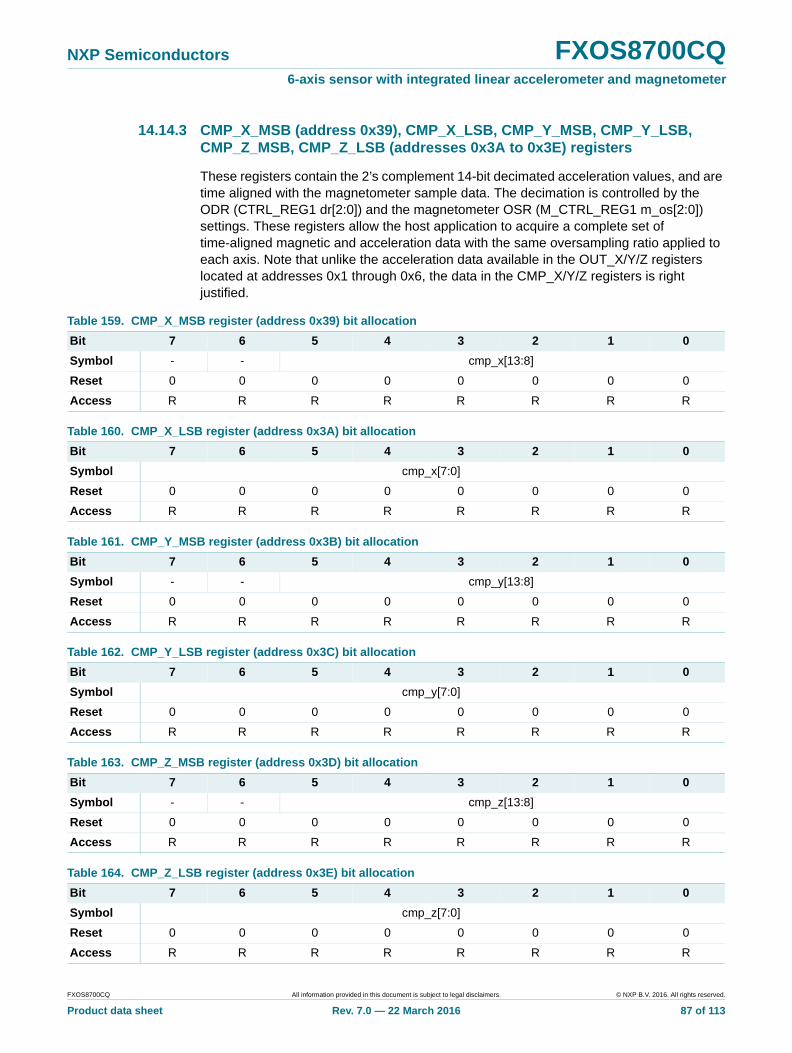
NXP Semiconductors FXOS8700CQ6-axis sensor with integrated linear accelerometer and magnetometer
14.14.3 CMP_X_MSB (address 0x39), CMP_X_LSB, CMP_Y_MSB, CMP_Y_LSB, CMP_Z_MSB, CMP_Z_LSB (addresses 0x3A to 0x3E) registers
These registers contain the 2’s complement 14-bit decimated acceleration values, and are time aligned with the magnetometer sample data. The decimation is controlled by the ODR (CTRL_REG1 dr[2:0]) and the magnetometer OSR (M_CTRL_REG1 m_os[2:0]) settings. These registers allow the host application to acquire a complete set of time-aligned magnetic and acceleration data with the same oversampling ratio applied to each axis. Note that unlike the acceleration data available in the OUT_X/Y/Z registers located at addresses 0x1 through 0x6, the data in the CMP_X/Y/Z registers is right justified.
Table 159. CMP_X_MSB register (address 0x39) bit allocation
Bit 7 6 5 4 3 2 1 0
Symbol - - cmp_x[13:8]
Reset 0 0 0 0 0 0 0 0
Access R R R R R R R R
Table 160. CMP_X_LSB register (address 0x3A) bit allocation
Bit 7 6 5 4 3 2 1 0
Symbol cmp_x[7:0]
Reset 0 0 0 0 0 0 0 0
Access R R R R R R R R
Table 161. CMP_Y_MSB register (address 0x3B) bit allocation
Bit 7 6 5 4 3 2 1 0
Symbol - - cmp_y[13:8]
Reset 0 0 0 0 0 0 0 0
Access R R R R R R R R
Table 162. CMP_Y_LSB register (address 0x3C) bit allocation
Bit 7 6 5 4 3 2 1 0
Symbol cmp_y[7:0]
Reset 0 0 0 0 0 0 0 0
Access R R R R R R R R
Table 163. CMP_Z_MSB register (address 0x3D) bit allocation
Bit 7 6 5 4 3 2 1 0
Symbol - - cmp_z[13:8]
Reset 0 0 0 0 0 0 0 0
Access R R R R R R R R
Table 164. CMP_Z_LSB register (address 0x3E) bit allocation
Bit 7 6 5 4 3 2 1 0
Symbol cmp_z[7:0]
Reset 0 0 0 0 0 0 0 0
Access R R R R R R R R
FXOS8700CQ All information provided in this document is subject to legal disclaimers. © NXP B.V. 2016. All rights reserved.
Product data sheet Rev. 7.0 — 22 March 2016 87 of 113
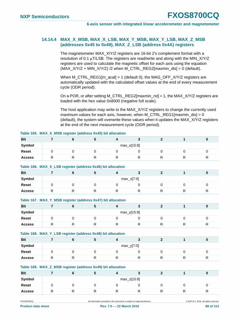
NXP Semiconductors FXOS8700CQ6-axis sensor with integrated linear accelerometer and magnetometer
14.14.4 MAX_X_MSB, MAX_X_LSB, MAX_Y_MSB, MAX_Y_LSB, MAX_Z_MSB (addresses 0x45 to 0x49), MAX_Z_LSB (address 0x4A) registers
The magnetometer MAX_X/Y/Z registers are 16-bit 2's complement format with a resolution of 0.1 μT/LSB. The registers are read/write and along with the MIN_X/Y/Z registers are used to calculate the magnetic offset for each axis using the equation (MAX_X/Y/Z + MIN_X/Y/Z) /2 when M_CTRL_REG2[maxmin_dis] = 0 (default).
When M_CTRL_REG1[m_acal] = 1 (default 0), the MAG_OFF_X/Y/Z registers are automatically updated with the calculated offset values at the end of every measurement cycle (ODR period).
On a POR, or after setting M_CTRL_REG2[maxmin_rst] = 1, the MAX_X/Y/Z registers are loaded with the hex value 0x8000 (negative full scale).
The host application may write to the MAX_X/Y/Z registers to change the currently used maximum values for each axis, however, when M_CTRL_REG1[maxmin_dis] = 0 (default), the system will overwrite these values when it updates the MAX_X/Y/Z registers at the end of the next measurement cycle (ODR period).
Table 165. MAX_X_MSB register (address 0x45) bit allocation
Bit 7 6 5 4 3 2 1 0
Symbol max_x[15:8]
Reset 0 0 0 0 0 0 0 0
Access R R R R R R R R
Table 166. MAX_X_LSB register (address 0x46) bit allocation
Bit 7 6 5 4 3 2 1 0
Symbol max_x[7:0]
Reset 0 0 0 0 0 0 0 0
Access R R R R R R R R
Table 167. MAX_Y_MSB register (address 0x47) bit allocation
Bit 7 6 5 4 3 2 1 0
Symbol max_y[15:8]
Reset 0 0 0 0 0 0 0 0
Access R R R R R R R R
Table 168. MAX_Y_LSB register (address 0x48) bit allocation
Bit 7 6 5 4 3 2 1 0
Symbol max_y[7:0]
Reset 0 0 0 0 0 0 0 0
Access R R R R R R R R
Table 169. MAX_Z_MSB register (address 0x49) bit allocation
Bit 7 6 5 4 3 2 1 0
Symbol max_z[15:8]
Reset 0 0 0 0 0 0 0 0
Access R R R R R R R R
FXOS8700CQ All information provided in this document is subject to legal disclaimers. © NXP B.V. 2016. All rights reserved.
Product data sheet Rev. 7.0 — 22 March 2016 88 of 113
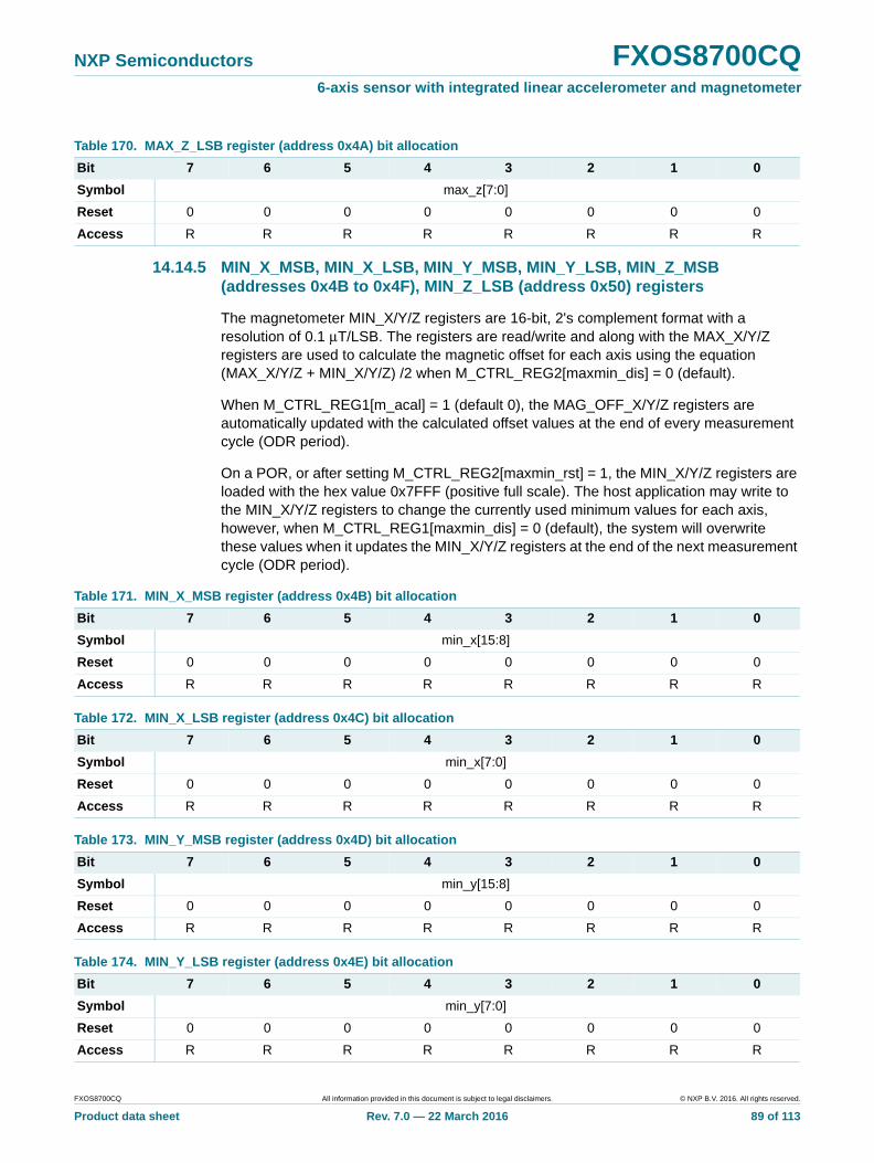
NXP Semiconductors FXOS8700CQ6-axis sensor with integrated linear accelerometer and magnetometer
14.14.5 MIN_X_MSB, MIN_X_LSB, MIN_Y_MSB, MIN_Y_LSB, MIN_Z_MSB (addresses 0x4B to 0x4F), MIN_Z_LSB (address 0x50) registers
The magnetometer MIN_X/Y/Z registers are 16-bit, 2's complement format with a resolution of 0.1 μT/LSB. The registers are read/write and along with the MAX_X/Y/Z registers are used to calculate the magnetic offset for each axis using the equation (MAX_X/Y/Z + MIN_X/Y/Z) /2 when M_CTRL_REG2[maxmin_dis] = 0 (default).
When M_CTRL_REG1[m_acal] = 1 (default 0), the MAG_OFF_X/Y/Z registers are automatically updated with the calculated offset values at the end of every measurement cycle (ODR period).
On a POR, or after setting M_CTRL_REG2[maxmin_rst] = 1, the MIN_X/Y/Z registers are loaded with the hex value 0x7FFF (positive full scale). The host application may write to the MIN_X/Y/Z registers to change the currently used minimum values for each axis, however, when M_CTRL_REG1[maxmin_dis] = 0 (default), the system will overwrite these values when it updates the MIN_X/Y/Z registers at the end of the next measurement cycle (ODR period).
Table 170. MAX_Z_LSB register (address 0x4A) bit allocation
Bit 7 6 5 4 3 2 1 0
Symbol max_z[7:0]
Reset 0 0 0 0 0 0 0 0
Access R R R R R R R R
Table 171. MIN_X_MSB register (address 0x4B) bit allocation
Bit 7 6 5 4 3 2 1 0
Symbol min_x[15:8]
Reset 0 0 0 0 0 0 0 0
Access R R R R R R R R
Table 172. MIN_X_LSB register (address 0x4C) bit allocation
Bit 7 6 5 4 3 2 1 0
Symbol min_x[7:0]
Reset 0 0 0 0 0 0 0 0
Access R R R R R R R R
Table 173. MIN_Y_MSB register (address 0x4D) bit allocation
Bit 7 6 5 4 3 2 1 0
Symbol min_y[15:8]
Reset 0 0 0 0 0 0 0 0
Access R R R R R R R R
Table 174. MIN_Y_LSB register (address 0x4E) bit allocation
Bit 7 6 5 4 3 2 1 0
Symbol min_y[7:0]
Reset 0 0 0 0 0 0 0 0
Access R R R R R R R R
FXOS8700CQ All information provided in this document is subject to legal disclaimers. © NXP B.V. 2016. All rights reserved.
Product data sheet Rev. 7.0 — 22 March 2016 89 of 113
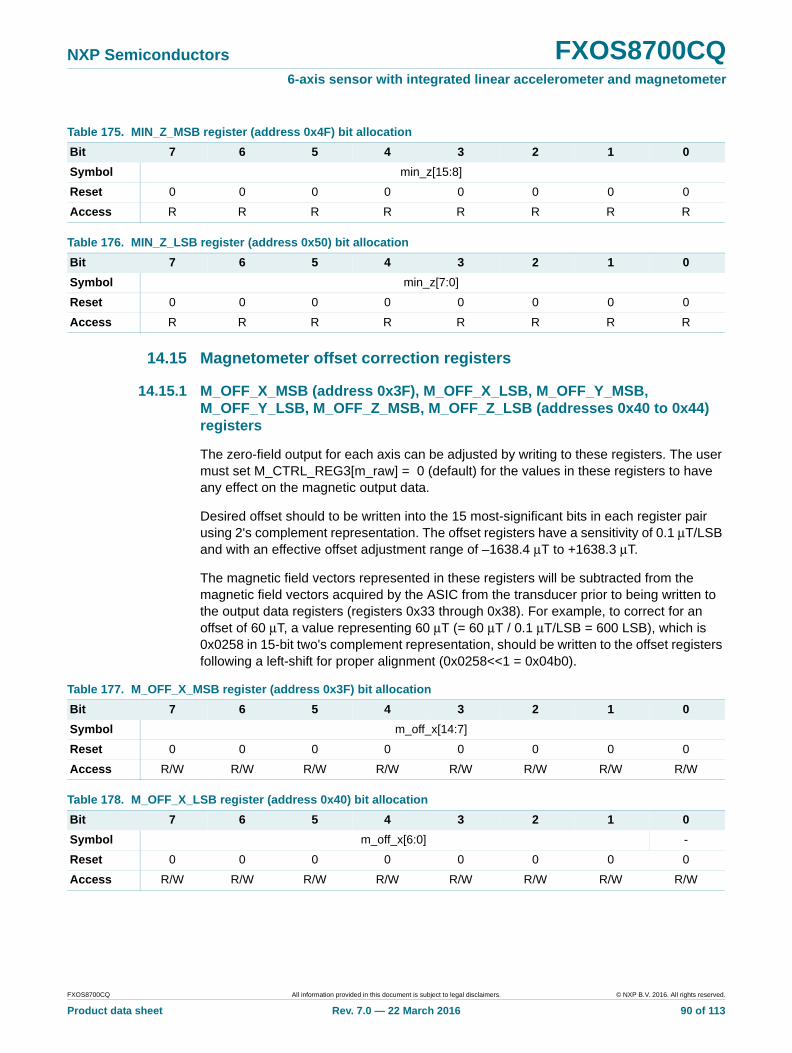
NXP Semiconductors FXOS8700CQ6-axis sensor with integrated linear accelerometer and magnetometer
14.15 Magnetometer offset correction registers
14.15.1 M_OFF_X_MSB (address 0x3F), M_OFF_X_LSB, M_OFF_Y_MSB, M_OFF_Y_LSB, M_OFF_Z_MSB, M_OFF_Z_LSB (addresses 0x40 to 0x44) registers
The zero-field output for each axis can be adjusted by writing to these registers. The user must set M_CTRL_REG3[m_raw] = 0 (default) for the values in these registers to have any effect on the magnetic output data.
Desired offset should to be written into the 15 most-significant bits in each register pair using 2's complement representation. The offset registers have a sensitivity of 0.1 μT/LSB and with an effective offset adjustment range of –1638.4 μT to +1638.3 μT.
The magnetic field vectors represented in these registers will be subtracted from the magnetic field vectors acquired by the ASIC from the transducer prior to being written to the output data registers (registers 0x33 through 0x38). For example, to correct for an offset of 60 μT, a value representing 60 μT (= 60 μT / 0.1 μT/LSB = 600 LSB), which is 0x0258 in 15-bit two's complement representation, should be written to the offset registers following a left-shift for proper alignment (0x0258<<1 = 0x04b0).
Table 175. MIN_Z_MSB register (address 0x4F) bit allocation
Bit 7 6 5 4 3 2 1 0
Symbol min_z[15:8]
Reset 0 0 0 0 0 0 0 0
Access R R R R R R R R
Table 176. MIN_Z_LSB register (address 0x50) bit allocation
Bit 7 6 5 4 3 2 1 0
Symbol min_z[7:0]
Reset 0 0 0 0 0 0 0 0
Access R R R R R R R R
Table 177. M_OFF_X_MSB register (address 0x3F) bit allocation
Bit 7 6 5 4 3 2 1 0
Symbol m_off_x[14:7]
Reset 0 0 0 0 0 0 0 0
Access R/W R/W R/W R/W R/W R/W R/W R/W
Table 178. M_OFF_X_LSB register (address 0x40) bit allocation
Bit 7 6 5 4 3 2 1 0
Symbol m_off_x[6:0] -
Reset 0 0 0 0 0 0 0 0
Access R/W R/W R/W R/W R/W R/W R/W R/W
FXOS8700CQ All information provided in this document is subject to legal disclaimers. © NXP B.V. 2016. All rights reserved.
Product data sheet Rev. 7.0 — 22 March 2016 90 of 113
NXP Semiconductors FXOS8700CQ6-axis sensor with integrated linear accelerometer and magnetometer
14.16 Magnetometer threshold function registers
The magnetometer threshold function works in a similar manner to the freefall/motion detection module but uses magnetic data for the event detection instead of acceleration data. The m_ths_oae bit setting determines the logic used to evaluate the threshold detection function for the enabled axes. With m_ths_oae = 0, the magnetic sample data for each enabled axis must be below the threshold values specified in the MAG_THS_X/Y/Z registers for the time period specified in MAG_THS_COUNT before the event flag is triggered. For m_ths_oae = 1, any of the enabled axes must be above the threshold values specified in the MAG_THS_X/Y/Z registers for the time period specified in MAG_THS_COUNT before the event flag is triggered.
14.16.1 M_THS_CFG register (address 0x52)
Magnetic-field threshold detection configuration register.
Table 179. M_OFF_Y_MSB register (address 0x41) bit allocation
Bit 7 6 5 4 3 2 1 0
Symbol m_off_y[14:7]
Reset 0 0 0 0 0 0 0 0
Access R/W R/W R/W R/W R/W R/W R/W R/W
Table 180. M_OFF_Y_LSB register (address 0x42) bit allocation
Bit 7 6 5 4 3 2 1 0
Symbol m_off_y[6:0] -
Reset 0 0 0 0 0 0 0 0
Access R/W R/W R/W R/W R/W R/W R/W R/W
Table 181. M_OFF_Z_MSB register (address 0x43) bit allocation
Bit 7 6 5 4 3 2 1 0
Symbol m_off_z[14:7]
Reset 0 0 0 0 0 0 0 0
Access R/W R/W R/W R/W R/W R/W R/W R/W
Table 182. M_OFF_Z_LSB register (address 0x44) bit allocation
Bit 7 6 5 4 3 2 1 0
Symbol m_off_z6:0] -
Reset 0 0 0 0 0 0 0 0
Access R/W R/W R/W R/W R/W R/W R/W R/W
Table 183. M_THS_CFG register (address 0x52) bit allocation
Bit 7 6 5 4 3 2 1 0
Symbol m_ths_ele m_ths_oae m_ths_zefe m_ths_yefe m_ths_xefe m_ths_wake_en m_ths_int_en m_ths_int_cfg
Reset 0 0 0 0 0 0 0 0
Access R/W R/W R/W R/W R/W R/W R/W R/W
FXOS8700CQ All information provided in this document is subject to legal disclaimers. © NXP B.V. 2016. All rights reserved.
Product data sheet Rev. 7.0 — 22 March 2016 91 of 113
NXP Semiconductors FXOS8700CQ6-axis sensor with integrated linear accelerometer and magnetometer
The unsigned 15-bit M_THS_X/Y/Z registers hold the threshold used for magnetic-event detection. With M_THS_CFG [m_ths_oae] = 0, the event is detected when all of the enabled axes are below or equal to their respective threshold values (AND condition). With M_THS_CFG [m_ths_oae] = 1, the event is detected when any of the enabled axes is above or equal to their respective threshold value (OR condition).
NOTEThe thresholds for each axis are applied on the magnetic data before it is corrected for the offset values stored in the M_OFF_X/Y/Z registers (when M_CTRL_REG3[m_raw] = 0). To apply thresholds on the user offset corrected data, it has to be implemented manually in the application software running on the MCU.
Table 184. M_THS_CFG register (address 0x52) bit descriptions
Field Description
m_ths_ele Magnetic-threshold event latch enable.
0 – Event flag latch disabled. Magnetic-threshold events are not latched, and the event flag will change state with the real-time status of the event detection logic.
1 – Event flag latch enabled. Magnetic-threshold events are latched and the event flag can only be cleared by reading the M_THS_SRC register.
m_ths_oae Magnetic-threshold event logic selection.
0 – Logical “AND” of enabled axes X, Y, and Z below threshold flags is used to detect the event.
1 – Logical “OR” of enabled axes X, Y, and Z above threshold flags is used to detect the event.
m_ths_zefe Event-flag enable on Z-axis.
0 – Z-axis event detection disabled
1 – Raise event flag on measured magnetic field value above/below preset threshold for Z-axis
m_ths_yefe Event-flag enable on Y-axis.
0 – Y-axis event detection disabled
1 – Raise event flag on measured magnetic field value above/below preset threshold for Y-axis
m_ths_xefe Event-flag enable on X-axis.
0 – X-axis event detection disabled
1 – Raise event flag on measured magnetic field value above/below preset threshold for X-axis
m_ths_wake_en 0 – The system excludes the magnetic-threshold event flag when evaluating the auto-sleep/wake function.1 – The system includes the magnetic-threshold event flag when evaluating the auto-sleep/wake function.
m_ths_int_en 0 – Magnetic-threshold interrupt is disabled.1 – Magnetic-threshold interrupt is enabled.
m_ths_int_cfg 0 – Magnetic-threshold event flag is output on INT2 pin (logically OR'd with other INT2 interrupt events)1 – Magnetic-threshold event flag is output on INT1 pin (logically OR'd with other INT1 interrupt events)
FXOS8700CQ All information provided in this document is subject to legal disclaimers. © NXP B.V. 2016. All rights reserved.
Product data sheet Rev. 7.0 — 22 March 2016 92 of 113
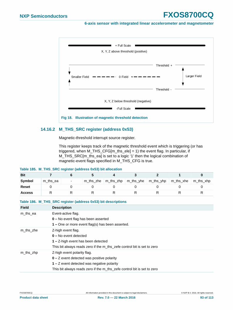
NXP Semiconductors FXOS8700CQ6-axis sensor with integrated linear accelerometer and magnetometer
14.16.2 M_THS_SRC register (address 0x53)
Magnetic-threshold interrupt source register.
This register keeps track of the magnetic threshold event which is triggering (or has triggered, when M_THS_CFG[m_ths_ele] = 1) the event flag. In particular, if M_THS_SRC[m_ths_ea] is set to a logic ‘1’ then the logical combination of magnetic-event flags specified in M_THS_CFG is true.
Fig 18. Illustration of magnetic threshold detection
0 Field
-Full Scale
+ Full Scale
Threshold +
Threshold -
X (Y, Z) High
X (Y, Z) High
Larger FieldSmaller Field
X, Y, Z above threshold (positive)
X, Y, Z below threshold (negative)
Table 185. M_THS_SRC register (address 0x53) bit allocation
Bit 7 6 5 4 3 2 1 0
Symbol m_ths_ea - m_ths_zhe m_ths_zhp m_ths_yhe m_ths_yhp m_ths_xhe m_ths_xhp
Reset 0 0 0 0 0 0 0 0
Access R R R R R R R R
Table 186. M_THS_SRC register (address 0x53) bit descriptions
Field Description
m_ths_ea Event-active flag.
0 – No event flag has been asserted
1 – One or more event flag(s) has been asserted.
m_ths_zhe Z-high event flag.
0 – No event detected
1 – Z-high event has been detected
This bit always reads zero if the m_ths_zefe control bit is set to zero
m_ths_zhp Z-high event polarity flag.
0 – Z event detected was positive polarity
1 – Z event detected was negative polarity
This bit always reads zero if the m_ths_zefe control bit is set to zero
FXOS8700CQ All information provided in this document is subject to legal disclaimers. © NXP B.V. 2016. All rights reserved.
Product data sheet Rev. 7.0 — 22 March 2016 93 of 113
NXP Semiconductors FXOS8700CQ6-axis sensor with integrated linear accelerometer and magnetometer
14.16.3 M_THS_X_MSB, M_THS_X_LSB, M_THS_Y_MSB, M_THS_Y_LSB, M_THS_Z_MSB, M_THS_Z_LSB (addresses 0x54 to 0x59) registers
The M_THS_X/Y/Z registers contain the unsigned 15-bit magnetic thresholds used by the magnetic-threshold function. Each register has a resolution of 0.1 μT/LSB. The thresholds for each axis are applied on the magnetic data before it is adjusted by the offset values stored in the M_OFF_X/Y/Z registers (when M_CTRL_REG3[m_raw] = 0). To apply thresholds on the user offset corrected data, it has to be implemented manually in the application
m_ths_yhe Y-high event flag.
0 – No event detected
1 – Y-high event has been detected
This bit always reads zero if the m_ths_yefe control bit is set to zero
m_ths_yhp Y-high event polarity flag.
0 – Y event detected was positive polarity
1 – Y event detected was negative polarity
This bit always reads zero if the m_ths_yefe control bit is set to zero
m_ths_xhe X-high event flag.
0 – No event detected
1 – X-high event has been detected
This bit always reads zero if the m_ths_xefe control bit is set to zero
m_ths_xhp X-high event polarity flag.
0 – X event detected was positive polarity
1 – X event detected was negative polarity.
This bit always reads zero if the m_ths_xefe control bit is set to zero
Table 186. M_THS_SRC register (address 0x53) bit descriptions - ¶continued
Field Description
Table 187. M_THS_X_MSB register (address 0x54) bit allocation
Bit 7 6 5 4 3 2 1 0
Symbol m_ths_dbcntm m_ths_x[14:8]
Reset 0 0 0 0 0 0 0 0
Access R/W R/W R/W R/W R/W R/W R/W R/W
Table 188. M_THS_X_MSB register (address 0x54) bit descriptions
Field Description
m_ths_dbcntm The m_ths_dbcntm bit configures the way in which the debounce counter is reset when the magnetic event of interest is momentarily not true.
When m_ths_dbcntm = 1, the debounce counter is cleared to 0 whenever the magnetic event of interest is no longer true.
When m_ths_dbcntm = 0, the debounce counter is decremented by 1 whenever the magnetic event of interest is no longer true.
m_ths_x[14:8] Upper 7 bits of the 15-bit unsigned X-axis magnetic threshold.
FXOS8700CQ All information provided in this document is subject to legal disclaimers. © NXP B.V. 2016. All rights reserved.
Product data sheet Rev. 7.0 — 22 March 2016 94 of 113
NXP Semiconductors FXOS8700CQ6-axis sensor with integrated linear accelerometer and magnetometer
14.16.4 M_THS_COUNT register (address 0x5A)
This register sets the number of debounce sample counts required before a magnetic threshold event is triggered.The behavior of the debounce counter is controlled by M_THS_X_MSB [m_ths_dbcntm].
Table 189. M_THS_X_LSB register (address 0x55) bit allocation
Bit 7 6 5 4 3 2 1 0
Symbol m_ths_x[7:0]
Reset 0 0 0 0 0 0 0 0
Access R/W R/W R/W R/W R/W R/W R/W R/W
Table 190. M_THS_Y_MSB register (address 0x56) bit allocation
Bit 7 6 5 4 3 2 1 0
Symbol - m_ths_y[14:8]
Reset 0 0 0 0 0 0 0 0
Access R/W R/W R/W R/W R/W R/W R/W R/W
Table 191. M_THS_Y_LSB register (address 0x57) bit allocation
Bit 7 6 5 4 3 2 1 0
Symbol m_ths_y[7:0]
Reset 0 0 0 0 0 0 0 0
Access R/W R/W R/W R/W R/W R/W R/W R/W
Table 192. M_THS_Z_MSB register (address 0x58) bit allocation
Bit 7 6 5 4 3 2 1 0
Symbol - m_ths_z[14:8]
Reset 0 0 0 0 0 0 0 0
Access R/W R/W R/W R/W R/W R/W R/W R/W
Table 193. M_THS_Z_LSB register (address 0x59) bit allocation
Bit 7 6 5 4 3 2 1 0
Symbol m_ths_z[7:0]
Reset 0 0 0 0 0 0 0 0
Access R/W R/W R/W R/W R/W R/W R/W R/W
Table 194. M_THS_COUNT register (address 0x5A) bit allocation
Bit 7 6 5 4 3 2 1 0
Symbol m_ths_cnt[7:0]
Reset 0 0 0 0 0 0 0 0
Access R/W R/W R/W R/W R/W R/W R/W R/W
Table 195. M_THS_COUNT register (address 0x5A) bit description
Field Description
m_ths_cnt[7:0] Magnetic threshold debounce count value.
FXOS8700CQ All information provided in this document is subject to legal disclaimers. © NXP B.V. 2016. All rights reserved.
Product data sheet Rev. 7.0 — 22 March 2016 95 of 113
NXP Semiconductors FXOS8700CQ6-axis sensor with integrated linear accelerometer and magnetometer
When the internal debounce counter reaches the M_THS_COUNT value a magnetic event flag is set. The debounce counter will never increase beyond the M_THS_COUNT value. The time step used for the debounce sample count depends on the chosen ODR. When hybrid mode is enabled, the effective ODR is reduced by a factor of two, which increases the debounce counter time step by a factor of two from what is shown in Table 196.
For example, an ODR of 100 Hz and a M_THS_COUNT value of 15 would result in a debounce response time of 150 ms. In hybrid mode, the same settings would result in a debounce response time of 300 ms.
Table 196. M_THS_COUNT relationship with the ODR
ODR (Hz) Time step (ms)
M_CTRL_REG1[m_hms] = 0b01 M_CTRL_REG1[m_hms] = 0b11
800 N/A N/A
400 2.5 5
200 5 10
100 10 20
50 20 40
12.5 80 160
6.25 160 320
1.56 641 1282
FXOS8700CQ All information provided in this document is subject to legal disclaimers. © NXP B.V. 2016. All rights reserved.
Product data sheet Rev. 7.0 — 22 March 2016 96 of 113
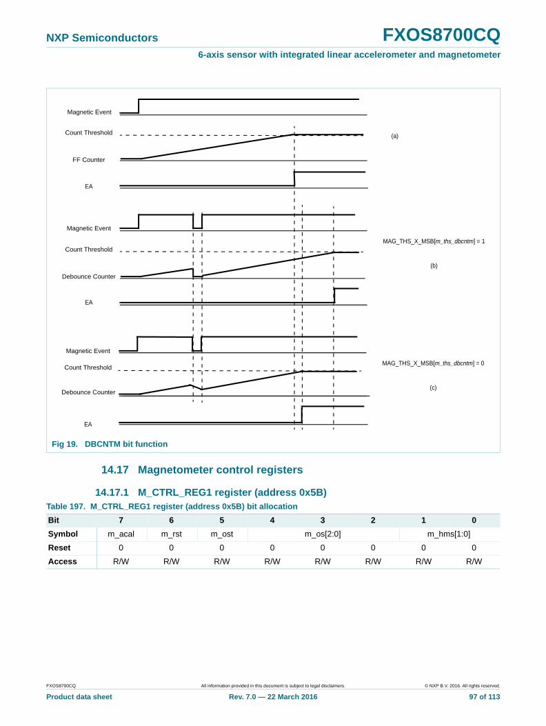
NXP Semiconductors FXOS8700CQ6-axis sensor with integrated linear accelerometer and magnetometer
14.17 Magnetometer control registers
14.17.1 M_CTRL_REG1 register (address 0x5B)
Fig 19. DBCNTM bit function
Table 197. M_CTRL_REG1 register (address 0x5B) bit allocation
Bit 7 6 5 4 3 2 1 0
Symbol m_acal m_rst m_ost m_os[2:0] m_hms[1:0]
Reset 0 0 0 0 0 0 0 0
Access R/W R/W R/W R/W R/W R/W R/W R/W
Magnetic Event
Count Threshold
EA
FF Counter
Magnetic Event
Count Threshold
(a)
Debounce Counter
Magnetic Event
Count Threshold
EA
MAG_THS_X_MSB[m_ths_dbcntm] = 1
(b)
EA
MAG_THS_X_MSB[m_ths_dbcntm] = 0
(c)Debounce Counter
FXOS8700CQ All information provided in this document is subject to legal disclaimers. © NXP B.V. 2016. All rights reserved.
Product data sheet Rev. 7.0 — 22 March 2016 97 of 113
NXP Semiconductors FXOS8700CQ6-axis sensor with integrated linear accelerometer and magnetometer
[1] When operating in hybrid mode, the effective ODR for each sensor is half of the frequency selected in the CTRL_REG1[dr] and CTRL_REG1[aslp_rate] bit fields.
The m_os[2:0] OSR setting along with the system ODR value set in CTRL_REG1 determines the magnetic output data update rate.
When m_hms[1:0] = 2'b11, magnetic output data is available in registers M_OUT_X_MSB (0x33), M_OUT_X_LSB (0x34), M_OUT_Y_MSB (0x35), M_OUT_Y_LSB (0x36), M_OUT_Z_MSB (0x37), and M_OUT_Z_LSB (0x38) along with the time synchronized accelerometer data in CMP_X_MSB (0x39), CMP_X_LSB (0x3A), CMP_Y_MSB (0x3B), CMP_Y_LSB (0x3C), CMP_Z_MSB (0x3D), and CMP_Z_LSB (0x3E).
NOTESwitching time from hybrid- or magnetometer-only mode (in active mode), to standby mode (after configuring it to standby mode) varies from 0 to 300 sec.
To eliminate a fixed amount of wait time for the device to go into standby mode:
• Configure the device into standby mode.
• Continously poll the SYSMOD (0x0B) register to check whether the device has gone to standby mode.
14.17.2 M_CTRL_REG2 register (address 0x5C)
Table 198. M_CTRL_REG1 register (address 0x5B) bit descriptions
Field Description
m_acal Magnetic hard-iron offset auto-calibration enable:
0 – Auto-calibration feature disabled
1 – Auto-calibration feature is enabled; the ASIC uses the maximum and minimum magnetic data to determine the hard iron offset value. The M_OFF_X/Y/Z registers are automatically loaded with (MAX_X/Y/Z + MIN_X/Y/Z)/2 for each axis at the end of every ODR cycle.
m_rst One-shot magnetic reset degauss control bit:
0 – No magnetic sensor reset is active
1 – One-shot magnetic reset is enabled, hardware cleared when complete.
m_ost One-shot triggered magnetic measurement mode:
0 – No action taken, or one-shot measurement complete.
1 – If device is in active mode no action is taken. If device is in standby mode, take one set of magnetic measurements, clear this bit, and return to standby mode.
m_os[2:0] Oversample ratio (OSR) for magnetometer data (see Table 203).
m_hms[1:0] 0b00 – Only accelerometer sensor is active
0b01 – Only magnetometer sensor is active
0b11 – Hybrid mode, both accelerometer and magnetometer sensors are active[1]
Table 199. M_CTRL_REG2 register (address 0x5C) bit allocation
Bit 7 6 5 4 3 2 1 0
Symbol - - hyb_autoinc_mode
m_maxmin_dis
m_maxmin_dis_ths
m_maxmin_rst
m_rst_cnt[1:0]
Reset 0 0 0 0 0 0 0 0
Access R/W R/W R/W R/W R/W R/W R/W R/W
FXOS8700CQ All information provided in this document is subject to legal disclaimers. © NXP B.V. 2016. All rights reserved.
Product data sheet Rev. 7.0 — 22 March 2016 98 of 113
NXP Semiconductors FXOS8700CQ6-axis sensor with integrated linear accelerometer and magnetometer
14.17.3 M_CTRL_REG3 register (address 0x5D)
Table 200. M_CTRL_REG2 register (address 0x5C) bit descriptions
Field Description
hyb_autoinc_mode With hyb_autoinc_mode = 1 and fast-read mode is disabled (CTRL_REG1 [f_read] = 0), the register address will automatically advance to register 0x33 (M_OUT_X_MSB) after reading register 0x06 (OUT_Z_LSB) in burst-read mode. For hyb_autoinc_mode = 1 and fast-read mode enabled (CTRL_REG1[f_read = 1) the register address will automatically advance to register 0x33 (M_OUT_X_MSB) after reading register 0x05 (OUT_Z_MSB) during a burst-read mode. Refer to the register map auto-increment address column for further information.
m_maxmin_dis Magnetic measurement max/min detection function disable:
0 – Magnetic min/max detection function is enabled (default).
1 – Magnetic min/max detection function is disabled.
When enabled, the magnetic min/max detection function will update the MAX_X/Y/Z and MIN_X/Y/Z
registers at the end of each ODR cycle with the maximum and minimum magnetic measurements from each axis. This is used along with the auto-cal feature (M_CTRL_REG1[m_acal] = 1) as a hardware based hard-iron offset compensation function.
m_maxmin_dis_ths Magnetic measurement min/max detection function disable using the magnetic threshold event trigger:
0 – No impact to magnetic min/max detection function on a magnetic threshold event
1 – Magnetic min/max detection function is disabled when magnetic threshold event is triggered
m_maxmin_rst Magnetic measurement min/max detection function reset:
0 – No reset sequence is active
1 – Setting this bit resets the MIN_X/Y/Z and MAX_X/Y/Z registers to 0x7FFF and 0x8000, respectively (positive and negative full-scale values).This bit is automatically cleared after the reset is completed.
m_rst_cnt[1:0] Magnetic sensor reset (degaussing) frequency:
0b00 – Automatic magnetic reset at the beginning of each ODR cycle (default).
0b01 – Automatic magnetic reset every 16 ODR cycles.
0b10 – Automatic magnetic reset every 512 ODR cycles.
0b11 – Automatic magnetic reset is disabled. Magnetic reset only occurs automatically on a transition from standby to active mode, or can be triggered manually by setting M_CTRL_REG1[m_rst] = 1
Table 201. M_CTRL_REG3 register (address 0x5D) bit allocation
Bit 7 6 5 4 3 2 1 0
Symbol m_raw m_aslp_os[2:0] m_ths_xyz_update
Reserved[2:0]
Reset 0 0 0 0 0 0 0 0
Access R/W R/W R/W R/W R/W R/W R/W R/W
FXOS8700CQ All information provided in this document is subject to legal disclaimers. © NXP B.V. 2016. All rights reserved.
Product data sheet Rev. 7.0 — 22 March 2016 99 of 113
NXP Semiconductors FXOS8700CQ6-axis sensor with integrated linear accelerometer and magnetometer
14.17.4 M_INT_SRC register (address 0x5E)
Table 202. M_CTRL_REG3 register (address 0x5D) bit descriptions
Field Description
m_raw Magnetic measurement RAW mode enable:
0 – Values stored in the M_OFF_X/Y/Z registers are applied to the magnetic sample data. This bit must be cleared in order for the automatic hard-iron compensation function to have any effect.
1 – Values stored in M_OFF_X/Y/Z are not applied to the magnetic sample data; automatic hard-iron compensation function does not have any effect on the output data.
m_aslp_os[2:0] Defines magnetometer OSR in auto-sleep mode. See Table 203.
m_ths_xyz_update This control bit defines which reference values are updated when the magnetic threshold event detection function triggers.0 – X, Y and Z reference values are all updated when the function triggers on any of the X, Y, or Z axes.1 – Only the reference value for the axis that triggered the detection event is updated.
Table 203. M-cell OSR versus ODR
ODR (Hz) OSR = 0 OSR = 1 OSR = 2 OSR = 3 OSR = 4 OSR = 5 OSR = 6 OSR = 7
1.56 16 16 32 64 128 256 512 1024
6.25 4 4 8 16 32 64 128 256
12.5 2 2 4 8 16 32 64 128
50 2 2 2 2 4 8 16 32
100 2 2 2 2 2 4 8 16
200 2 2 2 2 2 2 4 8
400 2 2 2 2 2 2 2 4
800 2 2 2 2 2 2 2 2
Table 204. M_INT_SRC register (address 0x5E) bit allocation
Bit 7 6 5 4 3 2 1 0
Symbol - - - - - src_m_ths src_m_vecm src_m_drdy
Reset 0 0 0 0 0 0 0 0
Access R R R R R R R R
Table 205. M_INT_SRC register (address 0x5E) bit description
Field Description
src_m_ths Magnetic threshold interrupt flag:
0 – Magnetic threshold event has not been detected.
1 – Magnetic threshold event has been detected.
src_m_vecm Magnetic vector-magnitude interrupt flag:
0 – Magnetic vector-magnitude change event has not been detected.
1 – Magnetic vector-magnitude change event has been detected.
src_m_drdy Magnetic data-ready interrupt flag:
0 – No new magnetic data is available.
1 – New magnetic data is available.
FXOS8700CQ All information provided in this document is subject to legal disclaimers. © NXP B.V. 2016. All rights reserved.
Product data sheet Rev. 7.0 — 22 March 2016 100 of 113
NXP Semiconductors FXOS8700CQ6-axis sensor with integrated linear accelerometer and magnetometer
14.18 Magnetometer vector-magnitude function registers
The magnetometer vector-magnitude function will generate an interrupt when
> M_VECM_THS value and t > M_VECM_CNT value. Where m_x_out, m_y_out, and m_z_out are the current decimated magnetometer output values, and m_x_ref, m_y_ref, and m_z_ref are the internally latched reference values. The user may program the M_VECM_THS and M_VECM_CNT registers to establish the conditions needed to detect a magnetic vector-magnitude change event. Depending on the values chosen for the reference values, this function may be configured to detect a magnetic field magnitude that is above a preset threshold (with reference values = 0), or a change in magnitude between two magnetic vectors greater than the preset threshold (with reference values non-zero). Please note x_ref, y_ref, z_ref are stored internally and are not observable by the user through the register interface. Refer to NXP application note AN4458.
14.18.1 M_VECM_CFG register (address 0x69)
m_x_out m_x_ref–( )2 m_y_out m_y_ref–( )2 m_z_out m_z_ref–( )2+ +
Table 206. M_VECM_CFG register (address 0x69) bit allocation
Bit 7 6 5 4 3 2 1 0
Symbol m_vecm_ele
m_vecm_initm
m_vecm_updm
m_vecm_en m_vecm_wake_en
m_vecm_init_en
m_vecm_init_cfg
m_vecm_ele
Reset 0 0 0 0 0 0 0 0
Access R/W R/W R/W R/W R/W R/W R/W R/W
Table 207. M_VECM_CFG register (address 0x69) bit descriptions
Field Description
m_vecm_ele Magnetic vector-magnitude event latch enable:
0 – Event latch disabled
1 – Event latch enabled
With event latching enabled, the src_m_vecm interrupt flag may only be cleared by reading the M_INT_SRC register. With event latching disabled, the src_m_vecm interrupt flag is updated in real time and may be cleared by the ASIC prior to the user reading the flag.
m_vecm_initm Magnetic vector-magnitude initialization mode:
0 – The ASIC uses the current magnetic output data as the initial reference values at the time the m_vecm_en bit is set.
1 – The ASIC uses the data stored in the M_VECM_X/Y/Z_INIT registers as the initial reference values at the time the m_vecm_en bit is set.
m_vecm_updm Magnetic vector-magnitude reference value update mode:
0 – The function updates the reference values with the current X, Y, and Z magnetic data when the event is triggered.
1 – The function does not update the reference values when the event is triggered.
Setting m_vecm_initm = 1 and m_vecm_updm = 1 allows the user to manually update the reference values using the M_VECM_INIT_X/Y/Z registers in real time when the function is enabled.
FXOS8700CQ All information provided in this document is subject to legal disclaimers. © NXP B.V. 2016. All rights reserved.
Product data sheet Rev. 7.0 — 22 March 2016 101 of 113
NXP Semiconductors FXOS8700CQ6-axis sensor with integrated linear accelerometer and magnetometer
14.18.2 M_VECM_THS_MSB register (address 0x6A)
14.18.3 M_VECM_THS_LSB register (address 0x6B)
m_vecm_en Magnetic vector-magnitude function enable:
0 – Function is disabled.
1 – Function is enabled, the ASIC will update the internal m_x/y/z_ref registers with either the current magnetic output data or the values stored in the M_VECM_INIT_X/Y/Z registers depending on the state of m_vecm_initm.
Note: The magnetic vector-magnitude function will only function correctly up to a maximum ODR of 400 Hz.
m_vecm_wake_en Magnetic vector-magnitude wake enable:
0 – The system excludes the src_m_vecm event flag when evaluating the auto-sleep function.
1 – The system includes the src_m_vecm event flag when evaluating the auto-sleep function.
m_vecm_int_en Magnetic vector-magnitude interrupt enable:
0 – Magnetic vector-magnitude interrupt is disabled.
1 – Magnetic vector-magnitude interrupt is enabled.
m_vecm_init_cfg Magnetic vector-magnitude interrupt configuration:
0 – Magnetic vector-magnitude interrupt is output on INT2 pin.
1 – Magnetic vector-magnitude interrupt is output on INT1 pin.
Table 207. M_VECM_CFG register (address 0x69) bit descriptions - ¶continued
Field Description
Table 208. M_VECM_THS_MSB register (address 0x6A) bit allocation
Bit 7 6 5 4 3 2 1 0
Symbol m_vecm_dbcntm
m_vecm_ths[14:8]
Reset 0 0 0 0 0 0 0 0
Access R/W R/W R/W R/W R/W R/W R/W R/W
Table 209. M_VECM_THS_MSB register (address 0x6A) bit descriptions
Field Description
m_vecm_dbcntm Magnetic vector-magnitude debounce counter mode selection:
0 – The debounce counter is decremented by 1 whenever the current vector-magnitude result is below the threshold set in M_VECM_THS.
1 – The debounce counter is cleared whenever the current vector-magnitude result is below the threshold set in M_VECM_THS.
m_vecm_ths[14:8] Seven most significant bits of 15-bit unsigned magnetic vector-magnitude threshold. Resolution is 0.1 μT/LSB.
Table 210. M_VECM_THS_LSB register (address 0x6B) bit allocation
Bit 7 6 5 4 3 2 1 0
Symbol m_vecm_ths[7:0]
Reset 0 0 0 0 0 0 0 0
Access R/W R/W R/W R/W R/W R/W R/W R/W
FXOS8700CQ All information provided in this document is subject to legal disclaimers. © NXP B.V. 2016. All rights reserved.
Product data sheet Rev. 7.0 — 22 March 2016 102 of 113
NXP Semiconductors FXOS8700CQ6-axis sensor with integrated linear accelerometer and magnetometer
14.18.4 M_VECM_CNT register (address 0x6C)
The debounce timer period is determined by the ODR selected in CTRL_REG1; it is equal to the number indicated in M_VECM_CNT register times 1/ODR. For example, a value of 16 in M_VECM_CNT with an ODR setting of 400 Hz will result in a debounce period of 40 ms. Note that ODR is halved when in hybrid mode.
14.18.5 M_VECM_INITX_MSB register (address 0x6D)
14.18.6 M_VECM_INITX_LSB register (address 0x6E)
Table 211. M_VECM_CNT register (address 0x6C) bit allocation
Bit 7 6 5 4 3 2 1 0
Symbol m_vecm_CNT[7:0]
Reset 0 0 0 0 0 0 0 0
Access R/W R/W R/W R/W R/W R/W R/W R/W
Table 212. M_VECM_CNT register (address 0x6C) bit description
Field Description
m_vecm_cnt[7:0] Vector-magnitude debounce count value.
Table 213. M_VECM_INITX_MSB register (address 0x6D) bit allocation
Bit 7 6 5 4 3 2 1 0
Symbol m_vecm_initx[15:8]
Reset 0 0 0 0 0 0 0 0
Access R/W R/W R/W R/W R/W R/W R/W R/W
Table 214. M_VECM_INITX_MSB register (address 0x6D) bit description
Field Description
m_vecm_initx[15:8] MSB of signed 16-bit initial X-axis value used by the magnetic vector-magnitude function when M_VECM_CFG[m_vecm_initm] = 1.
Table 215. M_VECM_INITX_LSB register (address 0x6E) bit allocation
Bit 7 6 5 4 3 2 1 0
Symbol m_vecm_initx[7:0]
Reset 0 0 0 0 0 0 0 0
Access R/W R/W R/W R/W R/W R/W R/W R/W
Table 216. M_VECM_INITX_LSB register (address 0x6E) bit description
Field Description
m_vecm_initx[7:0] LSB of signed 16-bit initial X-axis value used by the magnetic vector-magnitude function when M_VECM_CFG[m_vecm_initm] = 1.
FXOS8700CQ All information provided in this document is subject to legal disclaimers. © NXP B.V. 2016. All rights reserved.
Product data sheet Rev. 7.0 — 22 March 2016 103 of 113
NXP Semiconductors FXOS8700CQ6-axis sensor with integrated linear accelerometer and magnetometer
14.18.7 M_VECM_INITY_MSB register (address 0x6F)
14.18.8 M_VECM_INITY_LSB register (address 0x70)
14.18.9 M_VECM_INITZ_MSB register (address 0x71)
14.18.10 M_VECM_INITZ_LSB register (address 0x72)
Table 217. M_VECM_INITY_MSB register (address 0x6F) bit allocation
Bit 7 6 5 4 3 2 1 0
Symbol m_vecm_inity[15:8]
Reset 0 0 0 0 0 0 0 0
Access R/W R/W R/W R/W R/W R/W R/W R/W
Table 218. M_VECM_INITY_MSB register (address 0x6F) bit description
Field Description
m_vecm_inity[15:8] MSB of signed 16-bit initial Y-axis value used by the magnetic vector-magnitude function when M_VECM_CFG[m_vecm_initm] = 1.
Table 219. M_VECM_INITY_LSB register (address 0x70) bit allocation
Bit 7 6 5 4 3 2 1 0
Symbol m_vecm_inity[7:0]
Reset 0 0 0 0 0 0 0 0
Access R/W R/W R/W R/W R/W R/W R/W R/W
Table 220. M_VECM_INITY_LSB register (address 0x70) bit description
Field Description
m_vecm_inity[7:0] LSB of signed 16-bit initial Y-axis value used by the magnetic vector-magnitude function when M_VECM_CFG[m_vecm_initm] = 1.
Table 221. M_VECM_INITZ_MSB register (address 0x71) bit allocation
Bit 7 6 5 4 3 2 1 0
Symbol m_vecm_initz[15:8]
Reset 0 0 0 0 0 0 0 0
Access R/W R/W R/W R/W R/W R/W R/W R/W
Table 222. M_VECM_INITZ_MSB register (address 0x71) bit description
Field Description
m_vecm_initz[15:8] MSB of signed 16-bit initial Z-axis value used by the magnetic vector-magnitude function when M_VECM_CFG[m_vecm_initm] = 1.
Table 223. M_VECM_INITZ_LSB register (address 0x72) bit allocation
Bit 7 6 5 4 3 2 1 0
Symbol m_vecm_initz[15:8]
Reset 0 0 0 0 0 0 0 0
Access R/W R/W R/W R/W R/W R/W R/W R/W
Table 224. M_VECM_INITZ_LSB register (address 0x72) bit description
Field Description
m_vecm_initz[7:0] LSB of signed 16-bit initial Z-axis value used by the magnetic vector-magnitude function when M_VECM_CFG[m_vecm_initm] = 1.
FXOS8700CQ All information provided in this document is subject to legal disclaimers. © NXP B.V. 2016. All rights reserved.
Product data sheet Rev. 7.0 — 22 March 2016 104 of 113
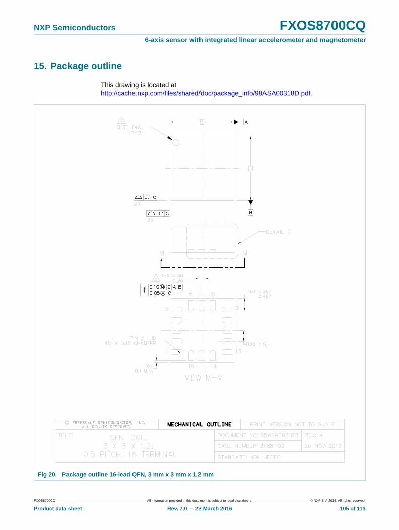
NXP Semiconductors FXOS8700CQ6-axis sensor with integrated linear accelerometer and magnetometer
15. Package outline
This drawing is located at http://cache.nxp.com/files/shared/doc/package_info/98ASA00318D.pdf.
Fig 20. Package outline 16-lead QFN, 3 mm x 3 mm x 1.2 mm
FXOS8700CQ All information provided in this document is subject to legal disclaimers. © NXP B.V. 2016. All rights reserved.
Product data sheet Rev. 7.0 — 22 March 2016 105 of 113
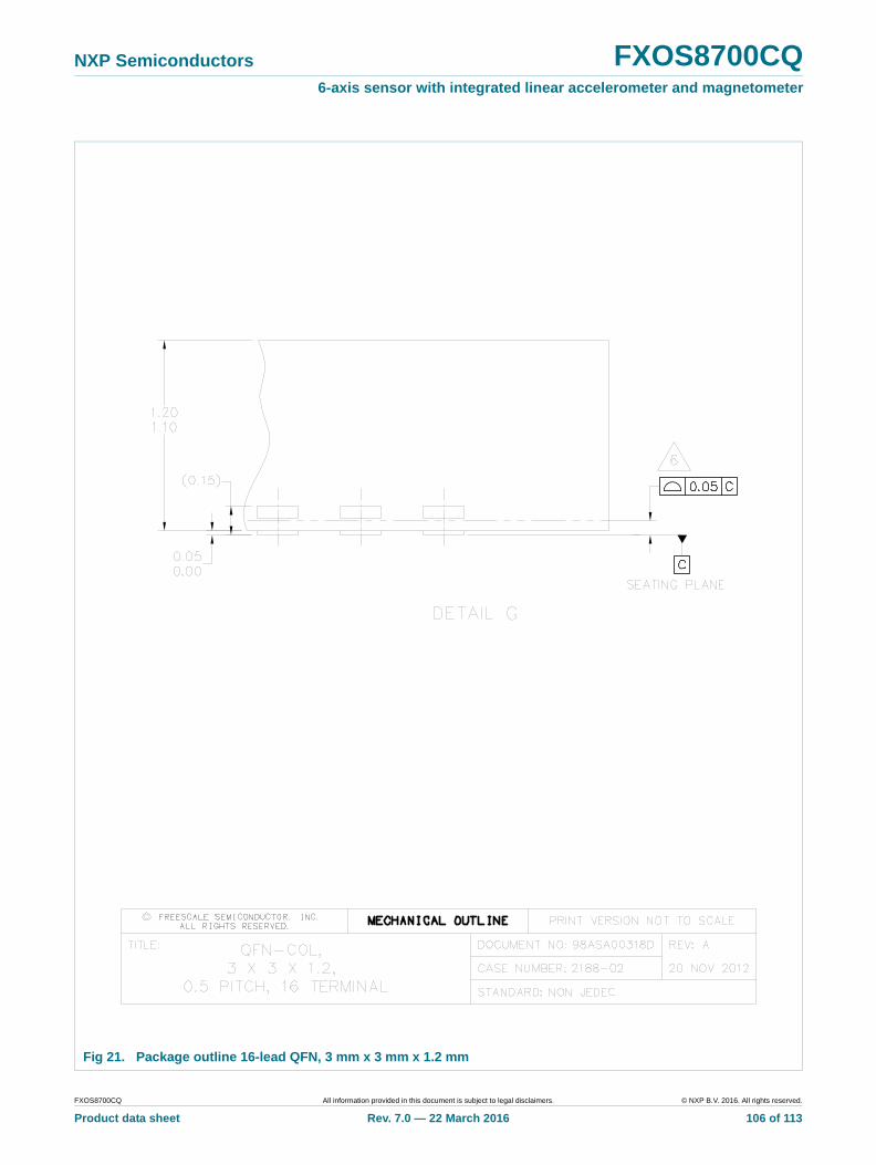
NXP Semiconductors FXOS8700CQ6-axis sensor with integrated linear accelerometer and magnetometer
Fig 21. Package outline 16-lead QFN, 3 mm x 3 mm x 1.2 mm
FXOS8700CQ All information provided in this document is subject to legal disclaimers. © NXP B.V. 2016. All rights reserved.
Product data sheet Rev. 7.0 — 22 March 2016 106 of 113
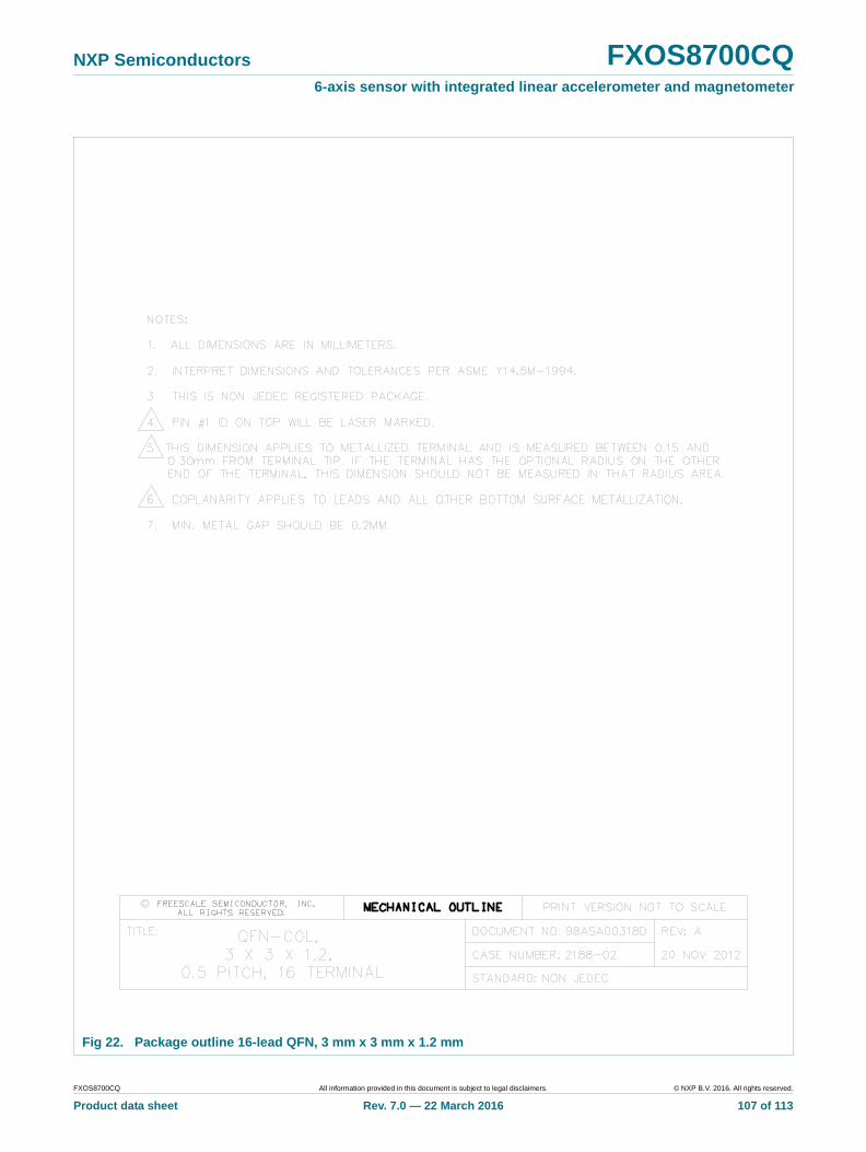
NXP Semiconductors FXOS8700CQ6-axis sensor with integrated linear accelerometer and magnetometer
Fig 22. Package outline 16-lead QFN, 3 mm x 3 mm x 1.2 mm
FXOS8700CQ All information provided in this document is subject to legal disclaimers. © NXP B.V. 2016. All rights reserved.
Product data sheet Rev. 7.0 — 22 March 2016 107 of 113
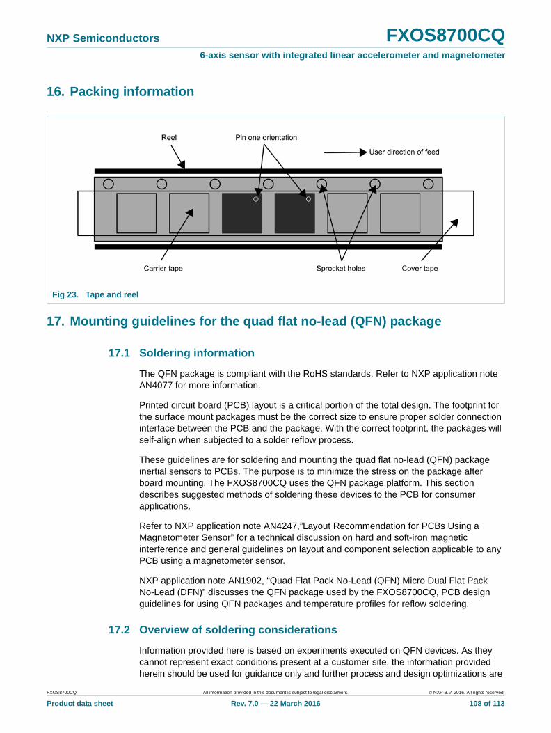
NXP Semiconductors FXOS8700CQ6-axis sensor with integrated linear accelerometer and magnetometer
16. Packing information
17. Mounting guidelines for the quad flat no-lead (QFN) package
17.1 Soldering information
The QFN package is compliant with the RoHS standards. Refer to NXP application note AN4077 for more information.
Printed circuit board (PCB) layout is a critical portion of the total design. The footprint for the surface mount packages must be the correct size to ensure proper solder connection interface between the PCB and the package. With the correct footprint, the packages will self-align when subjected to a solder reflow process.
These guidelines are for soldering and mounting the quad flat no-lead (QFN) package inertial sensors to PCBs. The purpose is to minimize the stress on the package after board mounting. The FXOS8700CQ uses the QFN package platform. This section describes suggested methods of soldering these devices to the PCB for consumer applications.
Refer to NXP application note AN4247,”Layout Recommendation for PCBs Using a Magnetometer Sensor” for a technical discussion on hard and soft-iron magnetic interference and general guidelines on layout and component selection applicable to any PCB using a magnetometer sensor.
NXP application note AN1902, “Quad Flat Pack No-Lead (QFN) Micro Dual Flat Pack No-Lead (DFN)” discusses the QFN package used by the FXOS8700CQ, PCB design guidelines for using QFN packages and temperature profiles for reflow soldering.
17.2 Overview of soldering considerations
Information provided here is based on experiments executed on QFN devices. As they cannot represent exact conditions present at a customer site, the information provided herein should be used for guidance only and further process and design optimizations are
Fig 23. Tape and reel
FXOS8700CQ All information provided in this document is subject to legal disclaimers. © NXP B.V. 2016. All rights reserved.
Product data sheet Rev. 7.0 — 22 March 2016 108 of 113
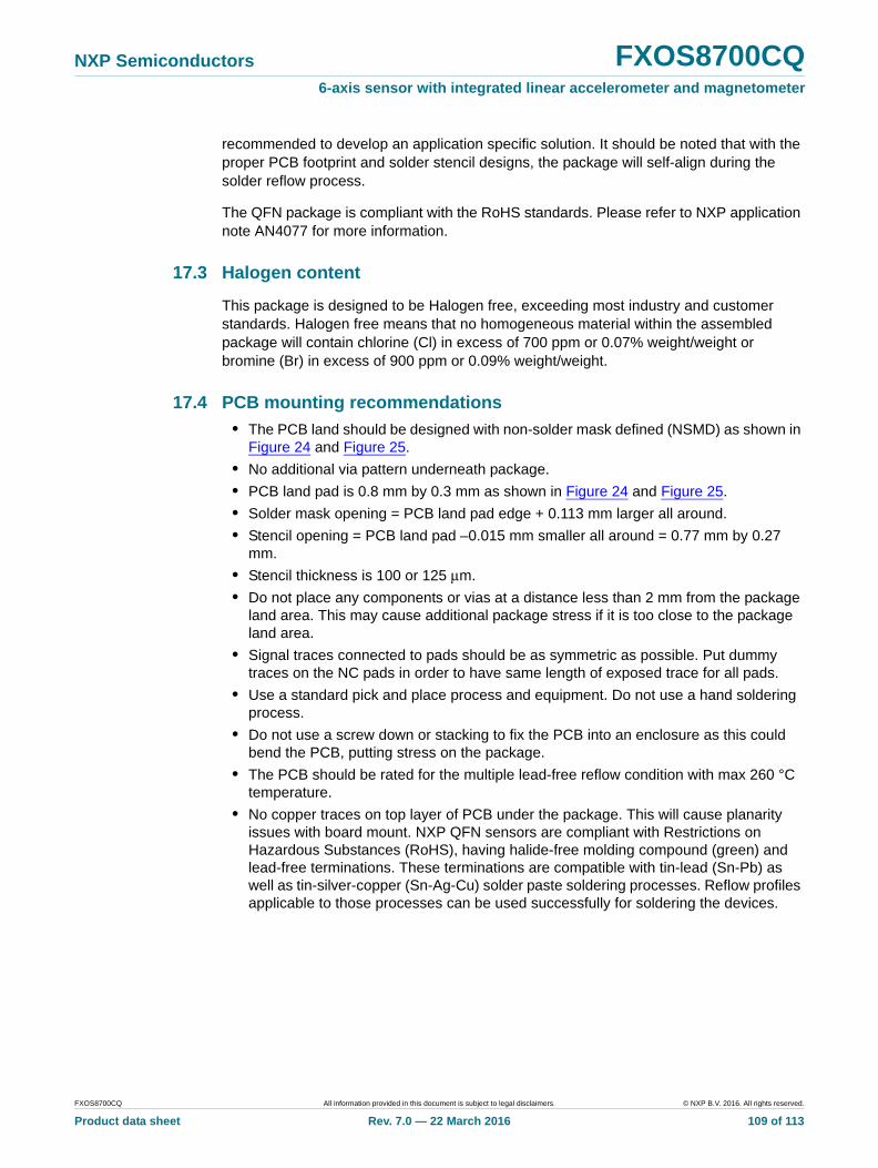
NXP Semiconductors FXOS8700CQ6-axis sensor with integrated linear accelerometer and magnetometer
recommended to develop an application specific solution. It should be noted that with the proper PCB footprint and solder stencil designs, the package will self-align during the solder reflow process.
The QFN package is compliant with the RoHS standards. Please refer to NXP application note AN4077 for more information.
17.3 Halogen content
This package is designed to be Halogen free, exceeding most industry and customer standards. Halogen free means that no homogeneous material within the assembled package will contain chlorine (Cl) in excess of 700 ppm or 0.07% weight/weight or bromine (Br) in excess of 900 ppm or 0.09% weight/weight.
17.4 PCB mounting recommendations
• The PCB land should be designed with non-solder mask defined (NSMD) as shown in Figure 24 and Figure 25.
• No additional via pattern underneath package.
• PCB land pad is 0.8 mm by 0.3 mm as shown in Figure 24 and Figure 25.
• Solder mask opening = PCB land pad edge + 0.113 mm larger all around.
• Stencil opening = PCB land pad –0.015 mm smaller all around = 0.77 mm by 0.27 mm.
• Stencil thickness is 100 or 125 μm.
• Do not place any components or vias at a distance less than 2 mm from the package land area. This may cause additional package stress if it is too close to the package land area.
• Signal traces connected to pads should be as symmetric as possible. Put dummy traces on the NC pads in order to have same length of exposed trace for all pads.
• Use a standard pick and place process and equipment. Do not use a hand soldering process.
• Do not use a screw down or stacking to fix the PCB into an enclosure as this could bend the PCB, putting stress on the package.
• The PCB should be rated for the multiple lead-free reflow condition with max 260 °C temperature.
• No copper traces on top layer of PCB under the package. This will cause planarity issues with board mount. NXP QFN sensors are compliant with Restrictions on Hazardous Substances (RoHS), having halide-free molding compound (green) and lead-free terminations. These terminations are compatible with tin-lead (Sn-Pb) as well as tin-silver-copper (Sn-Ag-Cu) solder paste soldering processes. Reflow profiles applicable to those processes can be used successfully for soldering the devices.
FXOS8700CQ All information provided in this document is subject to legal disclaimers. © NXP B.V. 2016. All rights reserved.
Product data sheet Rev. 7.0 — 22 March 2016 109 of 113
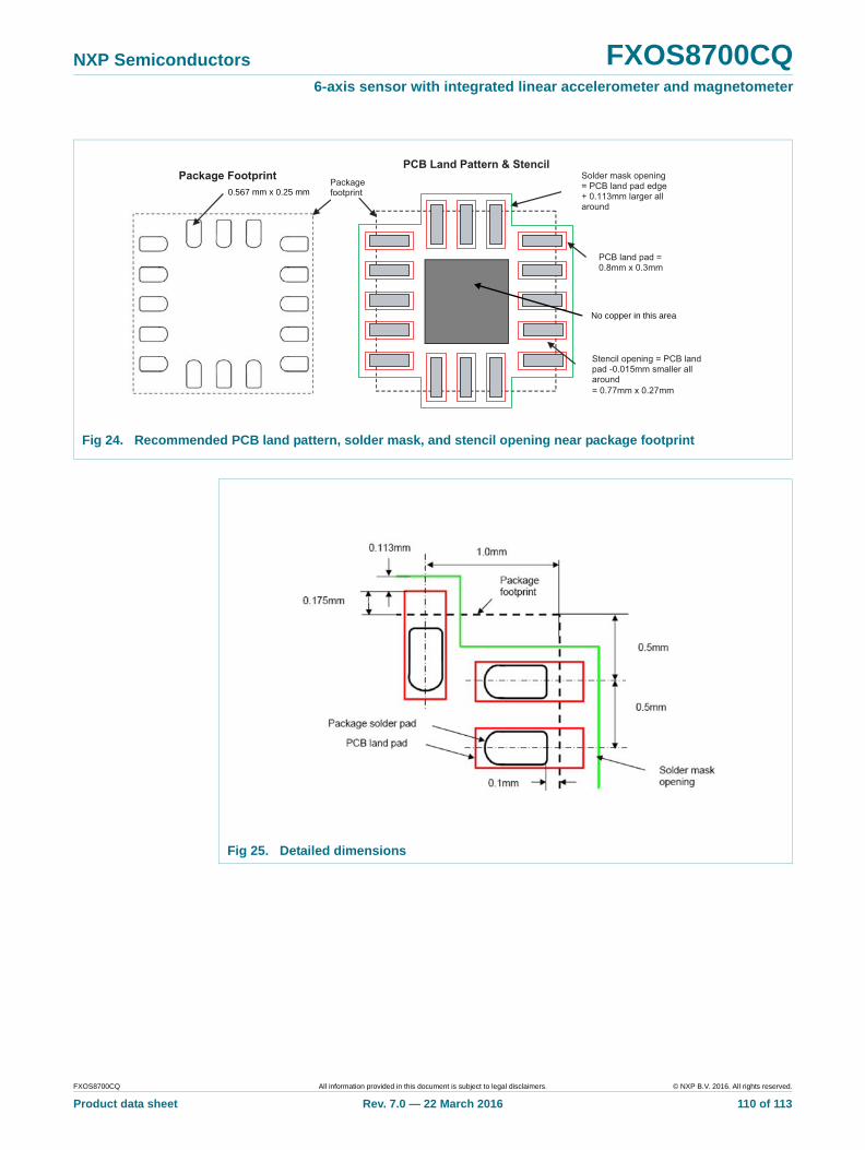
NXP Semiconductors FXOS8700CQ6-axis sensor with integrated linear accelerometer and magnetometer
Fig 24. Recommended PCB land pattern, solder mask, and stencil opening near package footprint
Packagefootprint0.467mm x 0.25mm
Package FootprintPCB Land Pattern & Stencil
Stencil opening = PCB landpad -0.015mm smaller allaround= 0.77mm x 0.27mm
Solder mask opening= PCB land pad edge+ 0.113mm larger allaround
PCB land pad =0.8mm x 0.3mm
0.567 mm x 0.25 mm
No copper in this area
Fig 25. Detailed dimensions
FXOS8700CQ All information provided in this document is subject to legal disclaimers. © NXP B.V. 2016. All rights reserved.
Product data sheet Rev. 7.0 — 22 March 2016 110 of 113
NXP Semiconductors FXOS8700CQ6-axis sensor with integrated linear accelerometer and magnetometer
18. Package thermal characteristics
[1] Junction temperature is a function of die size, on-chip power dissipation, package thermal resistance, mounting site (board) temperature, ambient temperature, air flow, power dissipation of other components on the board, and board thermal resistance.
[2] Per JEDEC JESD51-2 with the single-layer board (JESD51-3) horizontal.
[3] Per JEDEC JESD51-6 with the board (JESD51-7) horizontal.
[4] Thermal resistance between the die and the printed circuit board per JEDEC JESD51-8. Board temperature is measured on the top surface of the board near the package.
[5] Thermal resistance between the die and the case top surface as measured by the cold plate method (MIL SPEC-883 Method 1012.1).
[6] Thermal characterization parameter indicating the temperature difference between package top and the junction temperature per JEDEC JESD51-2. When Greek letters are not available, the thermal characterization parameter is written as Psi-JT.
Table 225. Thermal resistance data
Rating Description Symbol Value Unit
Junction-to-ambient, natural convection[1][2] Single-layer board RθJA 163 °C/W
Junction-to-ambient, natural convection[1][3] Four-layer board (two signals, two planes) 70
Junction-to-board[4] - RθJB 33 °C/W
Junction-to-case (top)[5] - RθJCTop 84 °C/W
Junction-to-package (top)[6] Natural convection ΨJT 6 °C/W
FXOS8700CQ All information provided in this document is subject to legal disclaimers. © NXP B.V. 2016. All rights reserved.
Product data sheet Rev. 7.0 — 22 March 2016 111 of 113
NXP Semiconductors FXOS8700CQ6-axis sensor with integrated linear accelerometer and magnetometer
19. Revision history
Table 226. Revision history
Document ID Release date Data sheet status Change notice Supersedes
FXOS8700CQ1 v.7.0 20160315 Product data sheet - FXOS8700CQ v.6
Modifications: • Global update: Removed instances of self-test for the magnetometer. Including update to last bullet on first page. Removed self-test input on magnetometer on Figure 1, updated Section 8.3, removed self-test output change row on Table 3 and removed magnetic self-test function bits on Table 201 and Table 202.
• Updated bullets in Section 2, features and benefits and Section 3, applications.
• Section 9.5: Table 8, updated value on maximum exposed magnetic field without perming row; was 10,000 to 3000.
• Section 14: Table 16, added and deleted footnote references.
• Section 14.1.5: Table 28, corrected description for sysmod[1:0] was “0b01: Sleep mode” to “0b10: Sleep mode”.
• Section 14.1.9: Table 37, updated description for rst, changing parts of paragraphs to a “Note”.
• Section 14.9.4: Table 86, corrected description for a_ffmt_ths_xyz_en• Section 14.17.1: Updated NOTE following Table 198.
• Added Section 16, Packing information.
FXOS8700CQ v.6.0 20150918 Product data sheet - FXOS8700CQ v.5.0
FXOS8700CQ v.5.0 20150527 Product data sheet - FXOS8700CQ v.4.1
FXOS8700CQ v.4.1 20150113 Product data sheet - FXOS8700CQ v.4.0
FXOS8700CQ v.4.0 20140305 Product data sheet - FXOS8700CQ v.3
FXOS8700CQ v.3 20130719 Product data sheet - FXOS8700CQ v.2
FXOS8700CQ v.2 20130511 Product data sheet - FXOS8700CQ v.1
FXOS8700CQ v.1 20120616 Advance information - -
FXOS8700CQ All information provided in this document is subject to legal disclaimers. © NXP B.V. 2016. All rights reserved.
Product data sheet Rev. 7.0 — 22 March 2016 112 of 113
NXP Semiconductors FXOS8700CQ6-axis sensor with integrated linear accelerometer and magnetometer
20. Legal information
20.1 Data sheet status
[1] Please consult the most recently issued document before initiating or completing a design.
[2] The product status of device(s) described in this document may have changed since this document was published and may differ in case of multiple devices. The latest product status information is available on the Internet at URL http://www.nxp.com.
Document status[1] Product status[2] Definition
Product preview Development This document contains certain information on a product under development. Freescale reserves the right to change or discontinue this product without notice.
Advance information Qualification This document contains information on a new product. Specifications and information herein are subject to change without notice.
Technical data Production NXP Semiconductors reserves the right to change the detail specifications as may be required to permit improvements in the design of its products.
FXOS8700CQ All information provided in this document is subject to legal disclaimers. © NXP B.V. 2016. All rights reserved.
Product data sheet Rev. 7.0 — 22 March 2016 113 of 113
NXP Semiconductors FXOS8700CQ6-axis sensor with integrated linear accelerometer and magnetometer
21. Contents
1 General description . . . . . . . . . . . . . . . . . . . . . . 1
2 Features and benefits . . . . . . . . . . . . . . . . . . . . 1
3 Applications . . . . . . . . . . . . . . . . . . . . . . . . . . . . 2
4 Ordering information. . . . . . . . . . . . . . . . . . . . . 2
5 Block diagram . . . . . . . . . . . . . . . . . . . . . . . . . . 3
6 Pinning information. . . . . . . . . . . . . . . . . . . . . . 46.1 Pinning . . . . . . . . . . . . . . . . . . . . . . . . . . . . . . . 46.2 Pin description . . . . . . . . . . . . . . . . . . . . . . . . . 5
7 Electrical connections. . . . . . . . . . . . . . . . . . . . 57.1 Orientation . . . . . . . . . . . . . . . . . . . . . . . . . . . . 7
8 Terminology . . . . . . . . . . . . . . . . . . . . . . . . . . . . 78.1 Sensitivity . . . . . . . . . . . . . . . . . . . . . . . . . . . . . 78.2 Zero-g and zero-flux offset . . . . . . . . . . . . . . . . 78.3 Self-test . . . . . . . . . . . . . . . . . . . . . . . . . . . . . . 8
9 Device characteristics. . . . . . . . . . . . . . . . . . . . 89.1 Accelerometer mechanical characteristics . . . . 89.2 Magnetometer magnetic characteristics . . . . . . 99.3 Hybrid characteristics . . . . . . . . . . . . . . . . . . . 109.4 Electrical characteristics . . . . . . . . . . . . . . . . . 109.5 Absolute maximum ratings . . . . . . . . . . . . . . . 12
10 Digital interfaces . . . . . . . . . . . . . . . . . . . . . . . 1310.1 I2C interface characteristics . . . . . . . . . . . . . . 1310.1.1 General I2C operation. . . . . . . . . . . . . . . . . . . 1410.1.2 I2C read/write operations . . . . . . . . . . . . . . . . 1510.2 SPI interface characteristics . . . . . . . . . . . . . . 1610.2.1 General SPI operation . . . . . . . . . . . . . . . . . . 1710.2.2 SPI read/write operations . . . . . . . . . . . . . . . . 1810.2.3 I2C/SPI auto detection . . . . . . . . . . . . . . . . . . 1910.2.4 Power supply sequencing and I2C/SPI mode
auto-detection. . . . . . . . . . . . . . . . . . . . . . . . . 19
11 Modes of operation . . . . . . . . . . . . . . . . . . . . . 19
12 Embedded functionality . . . . . . . . . . . . . . . . . 2012.1 Factory calibration . . . . . . . . . . . . . . . . . . . . . 2012.2 8-bit or 14-bit accelerometer data. . . . . . . . . . 2112.3 Accelerometer low-power modes versus
high-resolution modes . . . . . . . . . . . . . . . . . . 2112.4 Auto-wake/sleep mode . . . . . . . . . . . . . . . . . . 2112.5 Hybrid mode . . . . . . . . . . . . . . . . . . . . . . . . . . 2212.6 Accelerometer freefall and motion event detection
. . . . . . . . . . . . . . . . . . . . . . . . . . . . . . . . . . . . 2212.6.1 Freefall detection . . . . . . . . . . . . . . . . . . . . . . 2212.6.2 Motion detection . . . . . . . . . . . . . . . . . . . . . . . 2212.7 Transient detection . . . . . . . . . . . . . . . . . . . . . 2212.8 Pulse detection . . . . . . . . . . . . . . . . . . . . . . . . 2312.9 Orientation detection. . . . . . . . . . . . . . . . . . . . 23
12.10 Acceleration vector-magnitude detection. . . . 2312.11 Magnetic vector-magnitude detection . . . . . . 2412.12 Magnetic threshold detection . . . . . . . . . . . . . 2412.13 Magnetic min/max detection (autonomous
calibration) . . . . . . . . . . . . . . . . . . . . . . . . . . 24
13 Example FXOS8700CQ driver code. . . . . . . . 2513.1 Introduction . . . . . . . . . . . . . . . . . . . . . . . . . . 2513.2 FXOS8700CQ addresses . . . . . . . . . . . . . . . 2513.3 Sensor data structure. . . . . . . . . . . . . . . . . . . 2613.4 FXOS8700CQ configuration function. . . . . . . 2613.5 Data read function . . . . . . . . . . . . . . . . . . . . . 28
14 Register descriptions . . . . . . . . . . . . . . . . . . . 3014.1 Device configuration registers . . . . . . . . . . . . 3814.1.1 STATUS register (address 0x00) . . . . . . . . . . 3814.1.2 DR_STATUS register (address 0x00) . . . . . . 3814.1.3 F_STATUS register (address 0x00) . . . . . . . . 4014.1.4 TRIG_CFG register (address 0x0A) . . . . . . . 4014.1.5 SYSMOD register (address 0x0B) . . . . . . . . . 4114.1.6 INT_SOURCE register (address 0x0C) . . . . . 4114.1.7 WHO_AM_I register (address 0x0D) . . . . . . . 4314.1.8 CTRL_REG1 register (address 0x0A) . . . . . . 4314.1.9 CTRL_REG2 register (address 0x2B) . . . . . . 4514.1.10 CTRL_REG3 - interrupt control register (address
0x2C) . . . . . . . . . . . . . . . . . . . . . . . . . . . . . . . 4714.1.11 CTRL_REG4 - interrupt enable register (address
0x2D) . . . . . . . . . . . . . . . . . . . . . . . . . . . . . . . 4814.1.12 CTRL_REG5 - interrupt routing configuration
register (address 0x2E) . . . . . . . . . . . . . . . . . 4914.2 Auto-sleep trigger register . . . . . . . . . . . . . . . 5114.2.1 ASLP_COUNT register (address 0x29) . . . . . 5114.3 Temperature register . . . . . . . . . . . . . . . . . . . 5314.3.1 TEMP register (address 0x51) . . . . . . . . . . . . 5314.4 Accelerometer output data registers . . . . . . . 5314.4.1 OUT_X_MSB, OUT_X_LSB, OUT_Y_MSB,
OUT_Y_LSB, OUT_Z_MSB, OUT_Z_LSB (addresses 0x01 to 0x06) registers . . . . . . . . 53
14.5 Accelerometer FIFO register . . . . . . . . . . . . . 5514.5.1 F_SETUP register (address 0x09). . . . . . . . . 5514.6 Accelerometer sensor data configuration register
. . . . . . . . . . . . . . . . . . . . . . . . . . . . . . . . . . . . 5614.6.1 XYZ_DATA_CFG register (address 0x0E) . . . 5614.7 Accelerometer high-pass filter register . . . . . 5714.7.1 HP_FILTER_CUTOFF register (address 0x0F) 5714.8 Portrait/landscape detection registers . . . . . . 5814.8.1 PL_STATUS register (address 0x10) . . . . . . . 5914.8.2 PL_CFG register (address 0x11) . . . . . . . . . . 6014.8.3 PL_COUNT register (address 0x12) . . . . . . . 60
FXOS8700CQ All information provided in this document is subject to legal disclaimers. © NXP B.V. 2016. All rights reserved.
Product data sheet Rev. 7.0 — 21 March 2016 114 of 116
continued >>
NXP Semiconductors FXOS8700CQ6-axis sensor with integrated linear accelerometer and magnetometer
14.8.4 PL_BF_ZCOMP register (address 0x13) . . . . 6114.8.5 PL_THS_REG register (address 0x14) . . . . . 6214.9 Freefall and motion detection registers. . . . . . 6314.9.1 A_FFMT_CFG register (address 0x15) . . . . . 6314.9.2 A_FFMT_SRC register (address 0x16) . . . . . 6414.9.3 A_FFMT_THS register (address 0x17). . . . . . 6514.9.4 A_FFMT_ THS_X_MSB, A_FFMT_THS_X_LSB,
A_FFMT_THS_Y_MSB, A_FFMT_THS_Y_LSB, A_FFMT_THS_Z_MSB, A_FFMT_THS_Z_LSB registers (addresses 0x73 to 0x78) . . . . . . . . 66
14.9.5 A_FFMT_COUNT register (address 0x18) . . . 6814.10 Accelerometer vector-magnitude function register
. . . . . . . . . . . . . . . . . . . . . . . . . . . . . . . . . . . . 6914.10.1 A_VECM_CFG register (address 0x5F) . . . . . 7014.10.2 A_VECM_THS_MSB (address 0x60) register 7014.10.3 A_VECM_THS_LSB register (address 0x61) . 7114.10.4 A_VECM_CNT register (address 0x62) . . . . . 7114.10.5 A_VECM_INITX_MSB register (address 0x63) 7114.10.6 A_VECM_INITX_LSB register (address 0x64) 7214.10.7 A_VECM_INITY_MSB register (address 0x65) 7214.10.8 A_VECM_INITY_LSB register (address 0x66) 7214.10.9 A_VECM_INITZ_MSB register (address 0x67) 7214.10.10 A_VECM_INITZ_LSB register (address 0x68) 7314.11 Transient (AC) acceleration detection registers
. . . . . . . . . . . . . . . . . . . . . . . . . . . . . . . . . . . . 7314.11.1 TRANSIENT_CFG register (address 0x1D) . 7414.11.2 TRANSIENT_SRC register (address 0x1E) . . 7414.11.3 TRANSIENT_THS register (address 0x1F) . . 7514.11.4 TRANSIENT_COUNT register (address 0x20) 7614.12 Pulse detection registers . . . . . . . . . . . . . . . . 7714.12.1 PULSE_CFG register (address 0x21) . . . . . . 7714.12.2 PULSE_SRC register (address 0x22) . . . . . . 7814.12.3 PULSE_THSX register (address 0x23) . . . . . 7914.12.4 PULSE_THSY register (address 0x24) . . . . . 7914.12.5 PULSE_THSZ register (address 0x25). . . . . . 8014.12.6 PULSE_TMLT register (address 0x26). . . . . . 8014.12.7 PULSE_LTCY register (address 0x27) . . . . . . 8114.12.8 PULSE_WIND register (address 0x28) . . . . . 8214.13 Accelerometer offset correction registers . . . . 8314.13.1 OFF_X register (address 0x2F) . . . . . . . . . . . 8314.13.2 OFF_Y register (address 0x30) . . . . . . . . . . . 8414.13.3 OFF_Z register (address 0x31) . . . . . . . . . . . 8414.14 Magnetometer data registers . . . . . . . . . . . . . 8414.14.1 M_DR_STATUS register (address 0x32) . . . . 8414.14.2 M_OUT_X_MSB, M_OUT_X_LSB,
M_OUT_Y_MSB, M_OUT_Y_LSB, M_OUT_Z_MSB, M_OUT_Z_LSB registers (addresses 0x33 to 0x38) . . . . . . . . . . . . . . . . 86
14.14.3 CMP_X_MSB (address 0x39), CMP_X_LSB, CMP_Y_MSB, CMP_Y_LSB, CMP_Z_MSB, CMP_Z_LSB (addresses 0x3A to 0x3E) registers. . . . . . . . . . . . . . . . . . . . . . . . . . . . . . . . . . . . 87
14.14.4 MAX_X_MSB, MAX_X_LSB, MAX_Y_MSB, MAX_Y_LSB, MAX_Z_MSB (addresses 0x45 to 0x49), MAX_Z_LSB (address 0x4A) registers 88
14.14.5 MIN_X_MSB, MIN_X_LSB, MIN_Y_MSB, MIN_Y_LSB, MIN_Z_MSB (addresses 0x4B to 0x4F), MIN_Z_LSB (address 0x50) registers 89
14.15 Magnetometer offset correction registers. . . . 9014.15.1 M_OFF_X_MSB (address 0x3F),
M_OFF_X_LSB, M_OFF_Y_MSB, M_OFF_Y_LSB, M_OFF_Z_MSB, M_OFF_Z_LSB (addresses 0x40 to 0x44) registers . . . . . . . . . . . . . . . . . . . . . . . . . . . . . 90
14.16 Magnetometer threshold function registers . . 9114.16.1 M_THS_CFG register (address 0x52) . . . . . . 9114.16.2 M_THS_SRC register (address 0x53) . . . . . . 9314.16.3 M_THS_X_MSB, M_THS_X_LSB,
M_THS_Y_MSB, M_THS_Y_LSB, M_THS_Z_MSB, M_THS_Z_LSB (addresses 0x54 to 0x59) registers . . . . . . . . . . . . . . . . . 94
14.16.4 M_THS_COUNT register (address 0x5A) . . . 9514.17 Magnetometer control registers . . . . . . . . . . . 9714.17.1 M_CTRL_REG1 register (address 0x5B) . . . 9714.17.2 M_CTRL_REG2 register (address 0x5C) . . . 9814.17.3 M_CTRL_REG3 register (address 0x5D) . . . 9914.17.4 M_INT_SRC register (address 0x5E) . . . . . 10014.18 Magnetometer vector-magnitude function
registers . . . . . . . . . . . . . . . . . . . . . . . . . . . . 10114.18.1 M_VECM_CFG register (address 0x69) . . . 10114.18.2 M_VECM_THS_MSB register (address 0x6A)
. . . . . . . . . . . . . . . . . . . . . . . . . . . . . . . . . . . 10214.18.3 M_VECM_THS_LSB register (address 0x6B) 10214.18.4 M_VECM_CNT register (address 0x6C) . . . 10314.18.5 M_VECM_INITX_MSB register (address 0x6D)
. . . . . . . . . . . . . . . . . . . . . . . . . . . . . . . . . . . 10314.18.6 M_VECM_INITX_LSB register (address 0x6E)
. . . . . . . . . . . . . . . . . . . . . . . . . . . . . . . . . . . 10314.18.7 M_VECM_INITY_MSB register (address 0x6F)
. . . . . . . . . . . . . . . . . . . . . . . . . . . . . . . . . . . 10414.18.8 M_VECM_INITY_LSB register (address 0x70)
. . . . . . . . . . . . . . . . . . . . . . . . . . . . . . . . . . . 10414.18.9 M_VECM_INITZ_MSB register (address 0x71)
. . . . . . . . . . . . . . . . . . . . . . . . . . . . . . . . . . . 10414.18.10 M_VECM_INITZ_LSB register (address 0x72)
. . . . . . . . . . . . . . . . . . . . . . . . . . . . . . . . . . . 104
15 Package outline. . . . . . . . . . . . . . . . . . . . . . . 105
16 Packing information . . . . . . . . . . . . . . . . . . . 108
FXOS8700CQ All information provided in this document is subject to legal disclaimers. © NXP B.V. 2016. All rights reserved.
Product data sheet Rev. 7.0 — 21 March 2016 115 of 116
continued >>
NXP Semiconductors FXOS8700CQ6-axis sensor with integrated linear accelerometer and magnetometer
17 Mounting guidelines for the quad flat no-lead (QFN) package . . . . . . . . . . . . . . . . . . . . . . . . 108
17.1 Soldering information . . . . . . . . . . . . . . . . . . 10817.2 Overview of soldering considerations. . . . . . 10817.3 Halogen content . . . . . . . . . . . . . . . . . . . . . . 10917.4 PCB mounting recommendations. . . . . . . . . 109
18 Package thermal characteristics . . . . . . . . . 111
19 Revision history. . . . . . . . . . . . . . . . . . . . . . . 112
20 Legal information. . . . . . . . . . . . . . . . . . . . . . 113
© NXP B.V. 2016. All rights reserved.
For more information, please visit: http://www.nxp.comFor sales office addresses, please send an email to: [email protected]
Date of release: 21 March 2016
Document identifier: FXOS8700CQ
Please be aware that important notices concerning this document and the product(s)described herein, have been included in section ‘Legal information’.

Information in this document is provided solely to enable system and software implementers to use NXP products.
There are no expressed or implied copyright licenses granted hereunder to design or fabricate any integrated circuits
based on the information in this document. NXP reserves the right to make changes without further notice to any
products herein.
NXP makes no warranty, representation, or guarantee regarding the suitability of its products for any particular
purpose, nor does NXP assume any liability arising out of the application or use of any product or circuit, and
specifically disclaims any and all liability, including without limitation, consequential or incidental damages. "Typical"
parameters that may be provided in NXP data sheets and/or specifications can and do vary in different applications,
and actual performance may vary over time. All operating parameters, including "typicals," must be validated for each
customer application by the customer's technical experts. NXP does not convey any license under its patent rights nor
the rights of others. NXP sells products pursuant to standard terms and conditions of sale, which can be found at the
following address:
http://www.nxp.com/terms-of-use.html.
How to Reach Us:
Home Page: NXP.com
Web Support: http://www.nxp.com/support
NXP, the NXP logo, Freescale, and the Freescale logo, are trademarks of NXP B.V. All other product or service names
are the property of their respective owners. All rights reserved.
© 2016 NXP B.V.
Document Number: FXOS8700CQRev. 7.03/2016


![LG 50PJ350 Block Diagram [SCH]](https://img.pdfslide.tips/doc/110x75/577c83ce1a28abe054b6520e/lg-50pj350-block-diagram-sch.jpg)