Embed Size (px)
Citation preview

GaN HEMT Power Switch 의 특성 향상 방안
2004- 21648
최영환
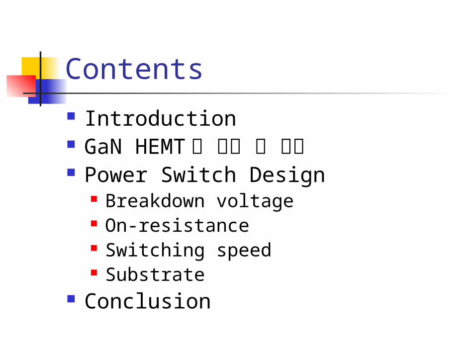
Contents Introduction GaN HEMT 의 구조 및 특성 Power Switch Design
Breakdown voltage On-resistance Switching speed Substrate
Conclusion

Introduction GaN 특성
Wide band gap (3.4 eV) Very low intrinsic carrier concentration High breakdown voltage (VB EG
5)
High electron mobility 2D e- Gas (1300 cm2/Vs ~ 2000 cm2/Vs) Bulk GaN (900 cm2/Vs)
High saturation velocity 약 1.5x107 cm/s

Introduction
Material Bandgap (eV)Electron mobility (cm2/Vs)
Critical electric
field (V/m)
Thermal conductivity (W/m
K)
Tmax
(℃)
Si 1.1 1300 300,000 130 300
GaAs 1.4 5000 400,000 55 300
SiC 2.9 260 2,300,000 110 600
GaN 3.4 900 3,000,000 700 700
Properties of Competing Material on Power Electronics

Introduction
• Breakdown voltage 와 specific on-resistance 비교
• 타 물질보다 우수한 특성
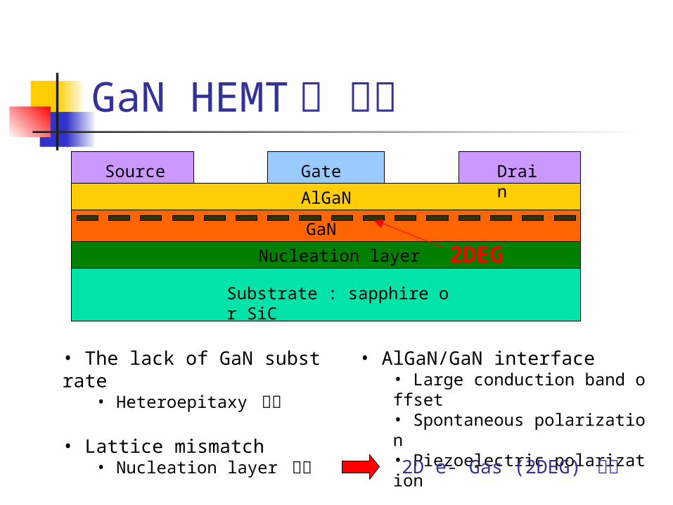
GaN HEMT 의 구조
Substrate : sapphire or SiC
Nucleation layer
GaN
AlGaN
Source DrainGate
2DEG
• AlGaN/GaN interface• Large conduction band offset• Spontaneous polarization• Piezoelectric polarization
2D e- Gas (2DEG) 형성
• The lack of GaN substrate• Heteroepitaxy 필요
• Lattice mismatch• Nucleation layer 생성

Power Switch Design (1) High breakdown voltage
Field crowding 방지 Circular design
Electric field 완화 Field plate
Impact ionization 억제 Low gate leakage current

Circular design
• Field crowding
• 소자의 blocking 특성 저하 • Circular device design
• Electric field 의 고른 분산
Blocking 능력 저하 방지
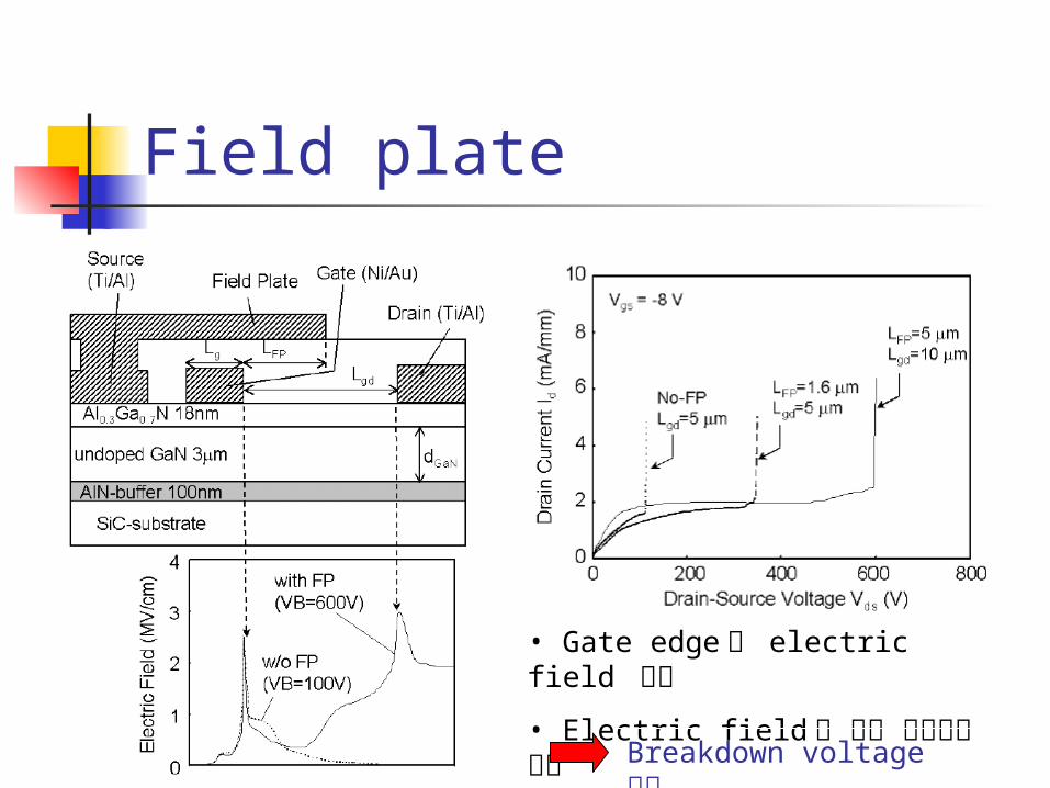
Field plate
• Gate edge 의 electric field 완화• Electric field 를 보다 균일하게 분산
Breakdown voltage 증가
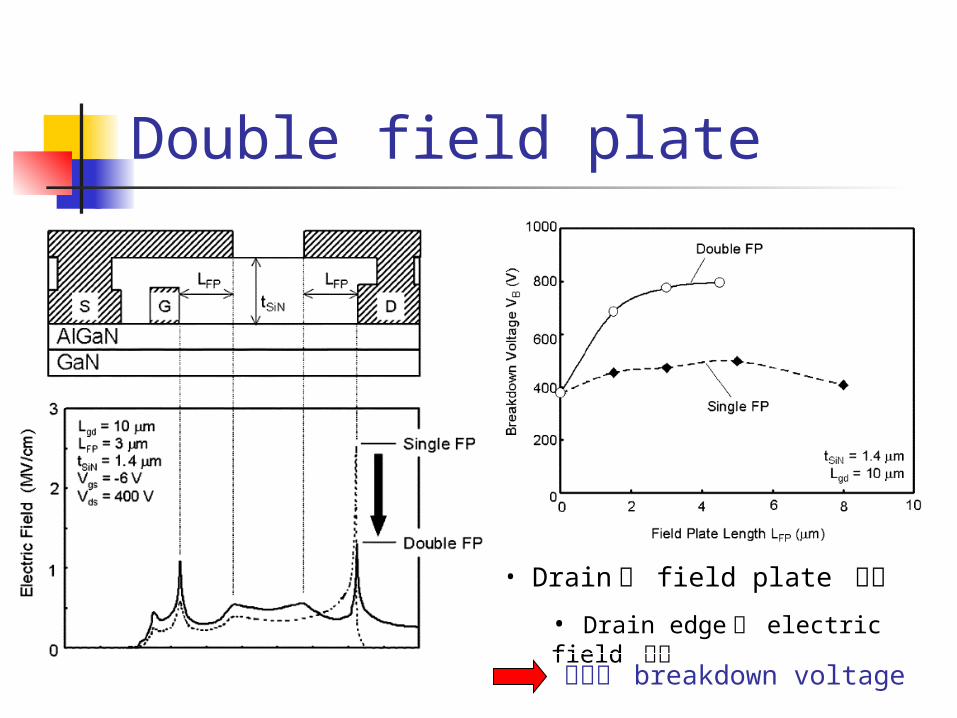
Double field plate
• Drain 에 field plate 추가• Drain edge 의 electric field 감소
향상된 breakdown voltage

Low gate leakage current
• Gate 절연막
• Gate leakage current 감소
• Impact ionization 억제
Breakdown voltage 증가

Power Switch Design (2) Low on-resistance
2DEG carrier density AlGaN layer 의 doping AlGaN layer 에 Al 함량 증가
Contact resistance Source/drain ohmic contact area Contact resistivity

RON-VB trade-off
• AlGaN layer doping 농도 증가 • Ohmic contact 면적 감소
• 낮은 contact resistivity
Breakdown voltage 감소
On-resistance 향상On-resistance 향상

Power Switch Design (3)
Switching speed Surface trap
Dielectric material Parasitic capacitance
Substrate

Surface trap
• Turn-off 상황• Gate 에서 electron 이 surface trap 으로 inject
• Channel 이 vertical depletion
• Electric field peak 감소
Breakdown voltage 증가

Dispersion
• I-V 특성 차이• Deep trap 에 의해서 발생• Slow emission process
• Dielectric material• SiN (shallow trap 형성 )• SiO2 (deep trap 형성 )
Switching speed 감소

Dielectric material 선택
• 이중 gate 절연막
• SiO2 와 Si3N4 의 장점을 결합
• Dispersion 감소• Shallow trap 형성
Switching speed 향상

Power Switch Design (4) Substrate
Conductive High breakdown voltage Large switching loss
Insulating Small switching loss Low breakdown voltage
SiC vs Sapphire Cost Thermal conductivity

SiC vs Sapphire (1)
• Sapphire substrate
• Breakdown voltage 감소
• Undoped AlGaN layer
• Gate leakage 감소

SiC vs Sapphire (2)
• Drain-source capacitance
• Switching speed 결정• Parasitic 성분이 dominant
• Insulating Substrate
• Parasitic capacitance 감소
Switching speed 향상
Power efficiency 향상
Switching speed 감소

Conclusion GaN HEMT
High power, high efficiency device GaN HEMT Design
Insulating substrate High breakdown voltage RONA 와 VB 의 trade-off 관계 개선 Shallow trap 형성
Future Work Epi 기술 개발 Cost 절감

Reference[1] UMESH K. MISHRA, FELLOW, IEEE, PRIMIT PARIKH, AND YI-FENG WU, “AlGaN/Ga
N HEMTs—An Overview of Device Operation and Applications”, Proceedings of The IEEE, VOL. 90, NO.6, June 2002
[2] S.J. Pearton, F. Ren, A.P. Zhang, K.P. Lee, “Fabrication and performance of GaN electronic devices”, Materials Science and Engineering, R30 pp. 55-212, 2000
[3] N.-Q. Zhang, B.Moran, S.P. DenBaars, U.K. Mishra, X.W.Wang and T.P.Ma, “Effects of surface traps on breakdown voltage and switching speed of GaN power switching HEMTs”, Electron Devices Meetings, IEDM Tech.Digest. pp.25.5.1-25.5.4, 2001
[4] Naiqian Zhang, Vivek Mehrotra, Sriram Chandrasekaran, Brendan Moran, Likun Shen, Umesh, Mishra, Edward Etzkorn and David Clarke, “Large Area GaN HEMT Power Devices for Power Electronic Applications: Switching and Temperature Characteristics”, IEEE Trans. Electron Device, pp 233-237. 2003

Reference[5] Wataru Saito, Yoshiharu Takada, Masahiko Kuraguchi, Kunio Tsuda, Ichiro Omur
a, Tsuneo Ogura, and Hiromichi Ohashi, “High Breakdown Voltage AlGaN–GaN Power-HEMT Design and High Current Density Switching Behavior”, IEEE Trans. Electron Device, VOL. 50, NO 12, 2003
[6] Wataru Saito, Masahiko Kuraguchi, Yoshiharu Takada, Kunio Tsuda, Ichiro Omura, and Tsuneo Ogura, “High Breakdown Voltage Undoped AlGaN–GaN Power HEMT on Sapphire Substrate and Its Demonstration for DC–DC Converter Application”, IEEE Trans. Electron Device, VOL. 51, NO. 11, 2004
[7] Wataru Saito, Masahiko Kuraguchi, Yoshiharu Takada, Kunio Tsuda and Ichiro Omura, “Design Optimization of High Breakdown Voltage AlGaN–GaN Power HEMT on an Insulating Substrate for RONA–VB Tradeoff Characteristics”, IEEE Trans. Electron Device, VOL. 52, NO. 1, 2005


![[PHPFest 2013] PHP 성능 향상 방법](https://img.pdfslide.tips/doc/110x75/5584c678d8b42aeb138b48b2/phpfest-2013-php-.jpg)