Embed Size (px)
Citation preview
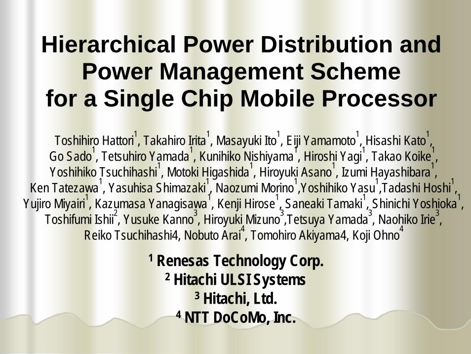
Hierarchical Power Distribution and Power Management Scheme
for a Single Chip Mobile ProcessorToshihiro Hattori1, Takahiro Irita1, Masayuki Ito1, Eiji Yamamoto1, Hisashi Kato1,
Go Sado1, Tetsuhiro Yamada1, Kunihiko Nishiyama1, Hiroshi Yagi1, Takao Koike1, Yoshihiko Tsuchihashi1, Motoki Higashida1, Hiroyuki Asano1, Izumi Hayashibara1,
Ken Tatezawa1, Yasuhisa Shimazaki1, Naozumi Morino1,Yoshihiko Yasu1,Tadashi Hoshi1,Yujiro Miyairi1, Kazumasa Yanagisawa1, Kenji Hirose1, Saneaki Tamaki1, Shinichi Yoshioka1,
Toshifumi Ishii2, Yusuke Kanno3, Hiroyuki Mizuno3,Tetsuya Yamada3, Naohiko Irie3,Reiko Tsuchihashi4, Nobuto Arai4, Tomohiro Akiyama4, Koji Ohno4
1 Renesas Technology Corp.2 Hitachi ULSI Systems
3 Hitachi, Ltd.4 NTT DoCoMo, Inc.
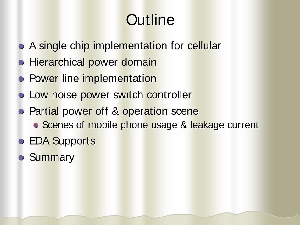
OutlineOutline
A single chip implementation for cellularA single chip implementation for cellularHierarchical power domainHierarchical power domainPower line implementationPower line implementationLow noise power switch controllerLow noise power switch controllerPartial power off & operation scenePartial power off & operation scene
Scenes of mobile phone usage & leakage currentScenes of mobile phone usage & leakage current
EDA SupportsEDA SupportsSummarySummary
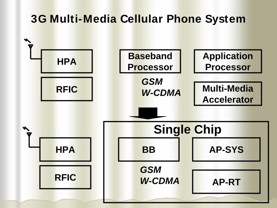
HPA
RFIC
BasebandProcessor
ApplicationProcessor
Multi-MediaAccelerator
GSMW-CDMA
HPA
RFIC
BB AP-SYS
AP-RTGSMW-CDMA
Single Chip
3G Multi-Media Cellular Phone System
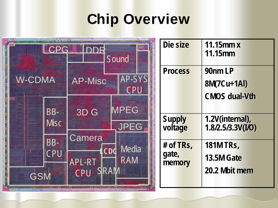
Die sizeDie size 11.1511.15mm x mm x 11.15mm11.15mm
# # of of TRsTRs, , gate, gate, memorymemory
181181M M TRsTRs, , 13.5M Gate 13.5M Gate 20.2 20.2 MbitMbit memmem
ProcessProcess 9090nm LPnm LP8M(7Cu+1Al)8M(7Cu+1Al)CMOS dualCMOS dual--VthVth
Supply Supply voltagevoltage
1.21.2V(internal), V(internal), 1.8/2.5/3.3V(I/O)1.8/2.5/3.3V(I/O)
GSM
W-CDMA
BB-CPU
APL-RTCPU
AP-SYSCPU
BB-Misc
AP-Misc
MediaRAM
3D G MPEG
Camera
SoundCPG
LCDC
JPEG
DDR
SRAM
Chip Overview
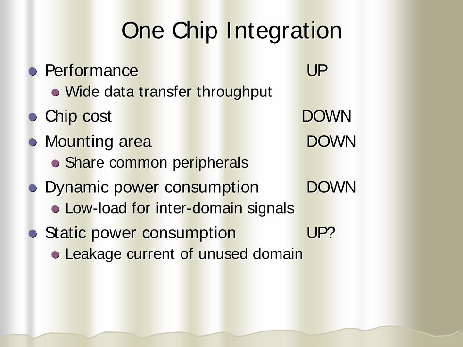
One Chip IntegrationOne Chip Integration
Performance Performance UPUPWide data transfer throughputWide data transfer throughput
Chip cost DOWNChip cost DOWNMounting area Mounting area DOWNDOWN
Share common peripheralsShare common peripherals
Dynamic power consumption Dynamic power consumption DOWNDOWNLowLow--load for interload for inter--domain signalsdomain signals
Static power consumption Static power consumption UP?UP?Leakage current of unused domain Leakage current of unused domain
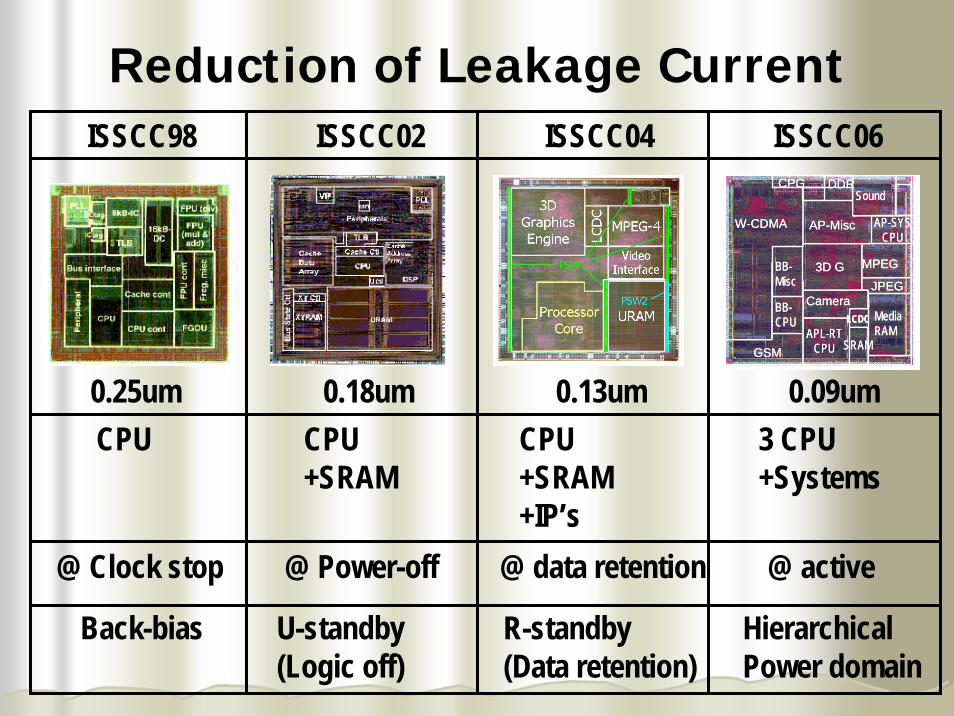
ISSCC98 ISSCC02 ISSCC04 ISSCC06
0.25um 0.18um 0.13um 0.09umCPU CPU
+SRAMCPU+SRAM+IP’s
3 CPU+Systems
Back-bias U-standby(Logic off)
R-standby(Data retention)
HierarchicalPower domain
@ Clock stop @ Power-off @ data retention @ active
GSM
W-CDMA
BB-CPU
APL-RTCPU
AP-SYSCPU
BB-Misc
AP-Misc
MediaRAM
3D G MPEG
Camera
SoundCPG
LCDC
JPEG
DDR
SRAMGSM
W-CDMA
BB-CPU
APL-RTCPU
AP-SYSCPU
BB-Misc
AP-Misc
MediaRAM
3D G MPEG
Camera
SoundCPG
LCDC
JPEG
DDR
SRAM
Reduction of Leakage Current
CPD
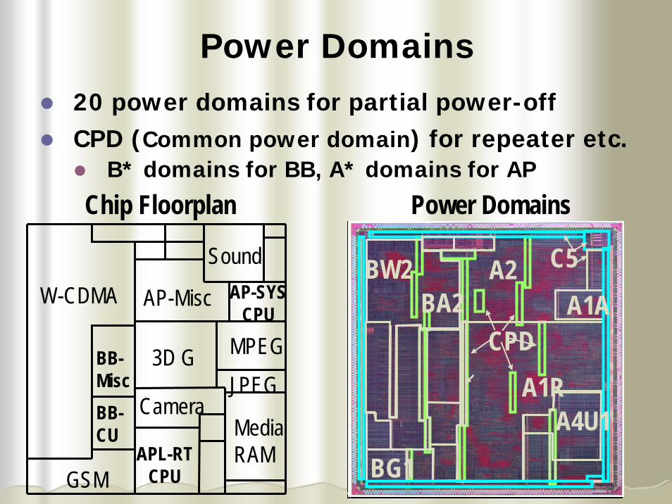
Chip Floorplan Power Domains
A1RA4U1
A1AA2 C5BW2
BG1
BA2
GSMAPL-RT
CPU
AP-SYSCPU
BB-Misc
AP-MiscW-CDMA
BB-CU Media
RAM
3D G MPEG
Camera
Sound
JPEG
Power Domains20 power domains for partial power-offCPD (Common power domain) for repeater etc.
B* domains for BB, A* domains for AP
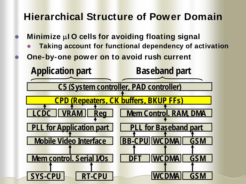
CPD (Repeaters, CK buffers, BKUP FFs)C5 (System controller, PAD controller)
LCDC Reg Mem Control. RAM, DMAVRAM
Application part Baseband part
PLL for Application part PLL for Baseband partMobile Video Interface
Mem control. Serial I/Os
SYS-CPU RT-CPU
BB-CPU WCDMA GSM
DFT WCDMA GSM
WCDMA GSM
CPD (Repeaters, CK buffers, BKUP FFs)
Hierarchical Structure of Power Domain
Minimize μIO cells for avoiding floating signalTaking account for functional dependency of activation
One-by-one power on to avoid rush current
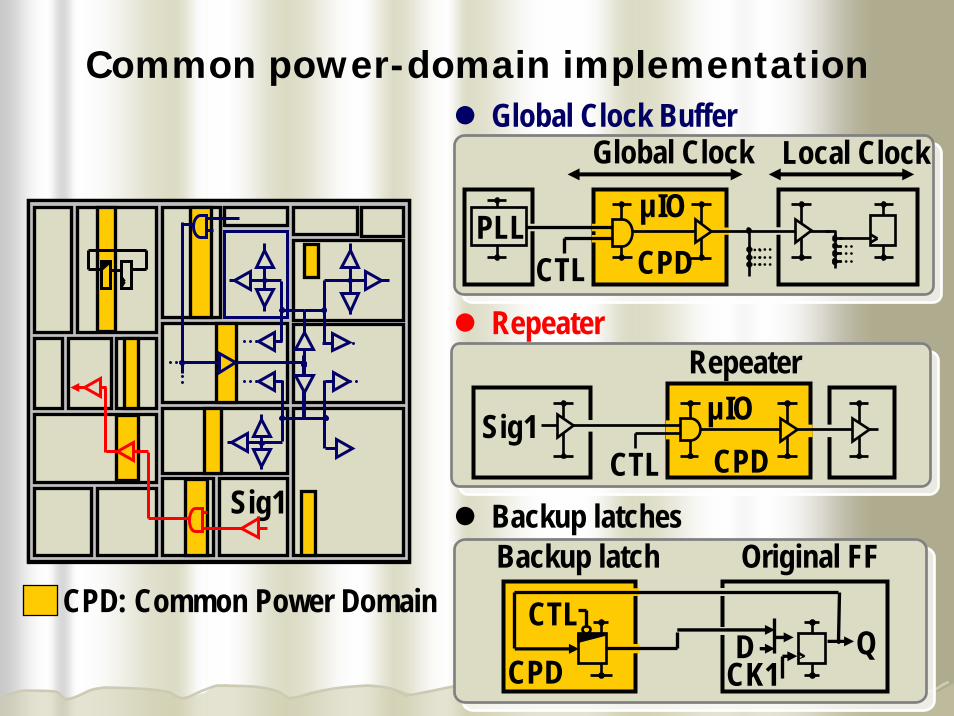
CPD: Common Power Domain
Sig1
Sig1CTL
µIOCPD
RepeaterRepeater
DCK1
QCTL
Backup latch Original FF
CPD
Backup latches
PLLCTL
µIOGlobal Clock Local Clock
CPD
Global Clock Buffer Common power-domain implementation
(thin ToxMOS)
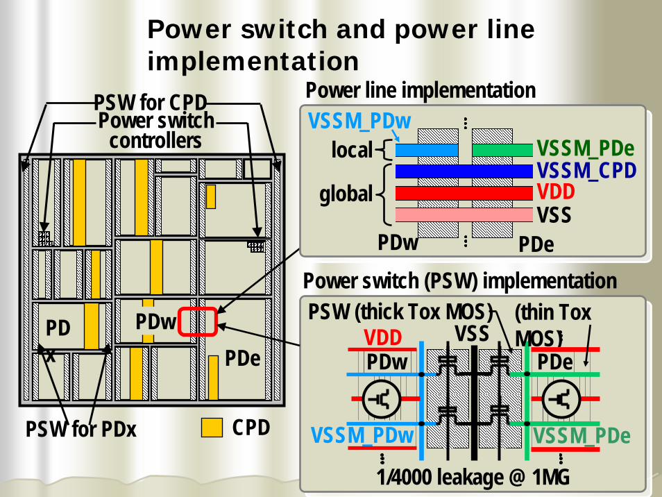
VSSM_PDe
PSW (thick Tox MOS)
PDeVSSVDD
CPDPSW for PDx
PDx
VSSM_PDw
PDw
PSW for CPD
Power switch (PSW) implementation
1/4000 leakage @ 1MG
VSSM_PDeVSSM_CPD
global
local
VDDVSS
VSSM_PDw
PDePDw
Power line implementation
PDwPDe
Power switch controllers
Power switch and power line implementation
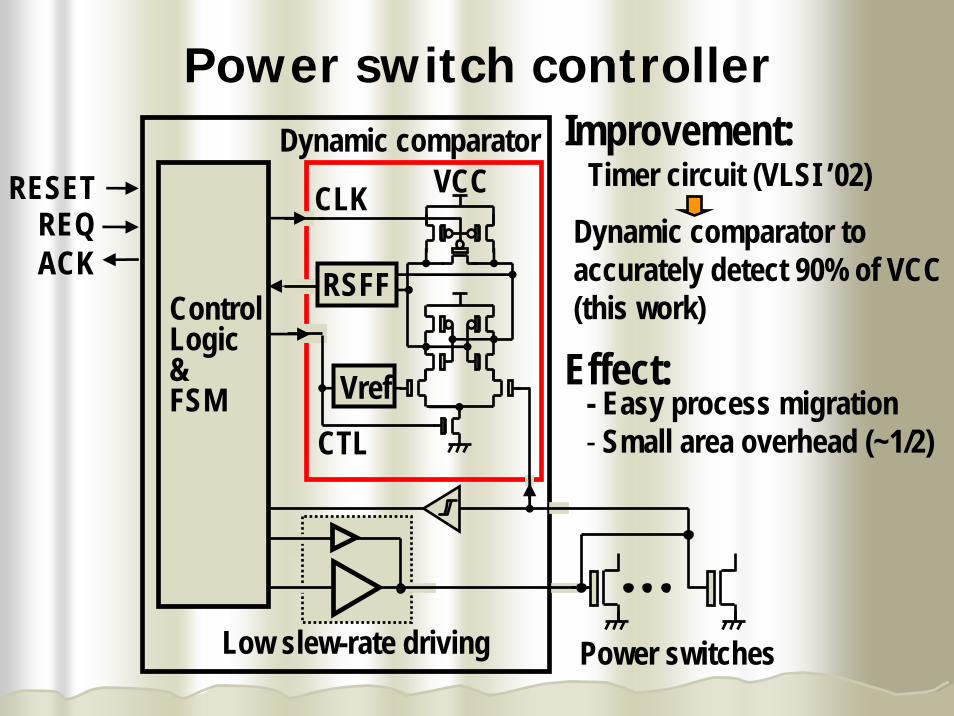
RESETREQACK
CTL
Dynamic comparatorVCCCLK
Vref
Control Logic & FSM
RSFF
Power switches
Improvement:Timer circuit (VLSI ’02)
Dynamic comparator toaccurately detect 90% of VCC(this work)
Effect:- Easy process migration- Small area overhead (~1/2)
Low slew-rate driving
Power switch controller

ACK
REQ
Rush current
3.9 µs
53.8 mA
Worst rush-current conditions
01234
0 5 10 150
20
40
60
Time (µs)
Volta
ge (V
)Cu
rrent
(m
A)
90% of VCC
Gate of the power switch
Simulated waveforms
3.9-µs recovery time and 53.8-mA rush current at 1 MG under worst rush-current conditions
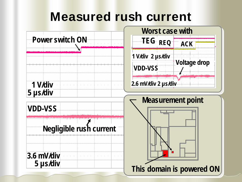
Power switch ON
VDD-VSS
Worst case with TEG REQ ACK
Voltage drop
This domain is powered ON
Measurement point
3.6 mV/div5 µs/div
1 V/div5 µs/div
2.6 mV/div 2 µs/div
1 V/div 2 µs/div
VDD-VSS
Negligible rush current
Measured rush current
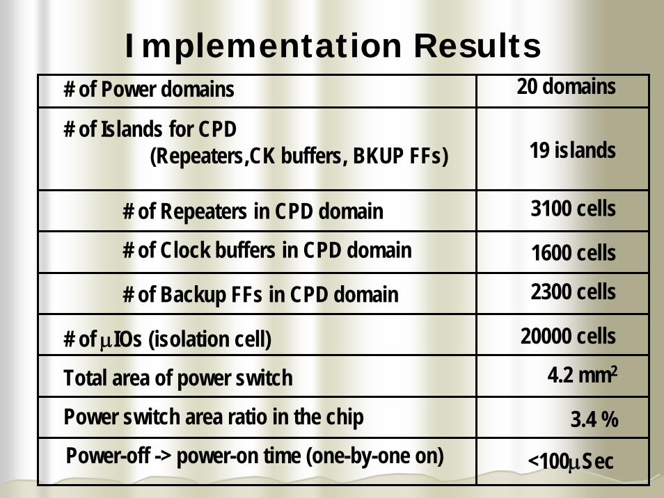
# of Power domains
# of Islands for CPD(Repeaters,CK buffers, BKUP FFs)
# of Repeaters in CPD domain# of Clock buffers in CPD domain
# of Backup FFs in CPD domain
# of μIOs (isolation cell)Total area of power switchPower switch area ratio in the chip
20 domains
19 islands
3100 cells
1600 cells2300 cells
20000 cells4.2 mm2
3.4 %Power-off -> power-on time (one-by-one on) <100μSec
Implementation Results
A1R
A4U2A3
A4U1
A1A
A2A4
C5AC
BW2
BA3
BW1
BG1 BG2BG3
BC
BA4BW3
C4
BA2
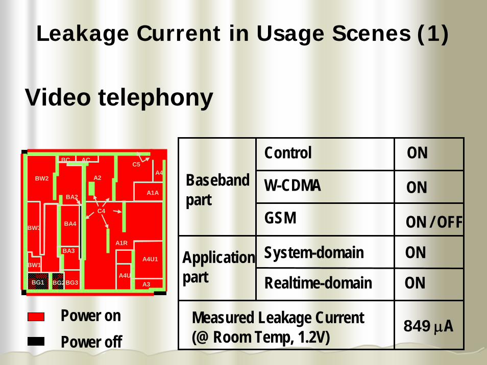
Video telephony
Measured Leakage Current (@ Room Temp, 1.2V)
Control
W-CDMA
GSM
System-domain
Realtime-domain
Basebandpart
Applicationpart
Power onPower off
ON
ON
ON / OFF
ON
ON
849 μA
Leakage Current in Usage Scenes (1)
Telephony (W-CDMA)
Measured Leakage Current (@ Room Temp, 1.2V)
Control
W-CDMA
GSM
System-domain
Realtime-domain
Basebandpart
Applicationpart
Power onPower off
ON
ON
ON / OFF
ON
OFF
407 μA
A1R
A4U2A3
A4U1
A1A
A2A4
C5AC
BW2
BA3
BW1
BG1 BG2BG3
BC
BA4BW3
C4
BA2
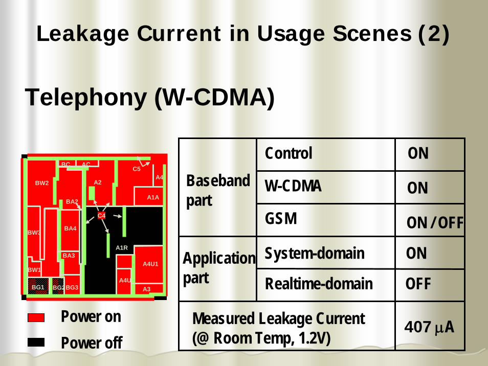
Leakage Current in Usage Scenes (2)
Waiting for Calling
Measured Leakage Current (@ Room Temp, 1.2V)
Control
W-CDMA
GSM
System-domain
Realtime-domain
Basebandpart
Applicationpart
Power onPower off
ON
OFF
OFF
OFF
OFF
299 μA
A1R
A4U2A3
A4U1
A1A
A2A4
C5AC
BW2
BA3
BW1
BG1 BG2BG3
BC
BA4BW3
C4
BA2
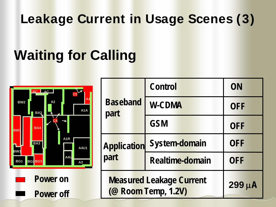
Leakage Current in Usage Scenes (3)
Power off ( I/O fixed)
Measured Leakage Current (@ Room Temp, 1.2V)
Control
W-CDMA
GSM
System-domain
Realtime-domain
Basebandpart
Applicationpart
Power onPower off
OFF
OFF
OFF
OFF
OFF
7 μA
A1R
A4U2A3
A4U1
A1A
A2A4
C5AC
BW2
BA3
BW1
BG1 BG2BG3
BC
BA4BW3
C4
BA2
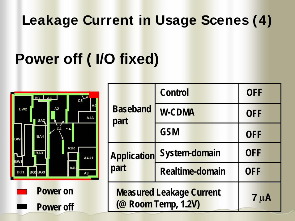
Leakage Current in Usage Scenes (4)
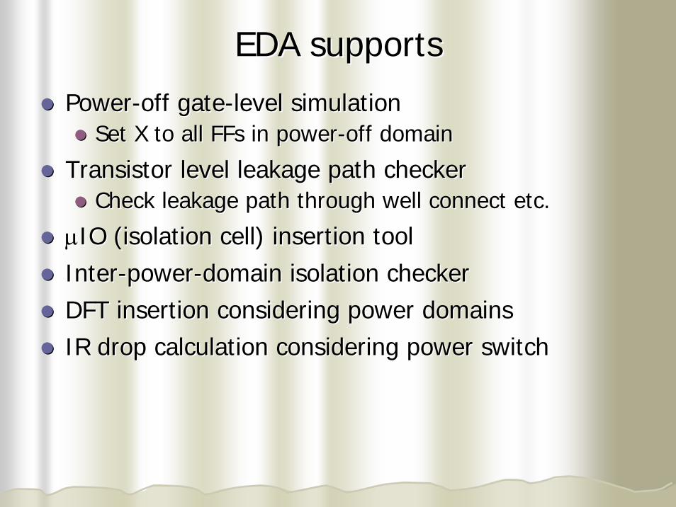
EDA supportsEDA supports
PowerPower--off gateoff gate--level simulationlevel simulationSet X to all Set X to all FFsFFs in powerin power--off domain off domain
Transistor level leakage path checkerTransistor level leakage path checkerCheck leakage path through well connect etc.Check leakage path through well connect etc.
μμIOIO (isolation cell) insertion tool(isolation cell) insertion tool
InterInter--powerpower--domain isolation checkerdomain isolation checkerDFT insertion considering power domainsDFT insertion considering power domainsIR drop calculation considering power switchIR drop calculation considering power switch
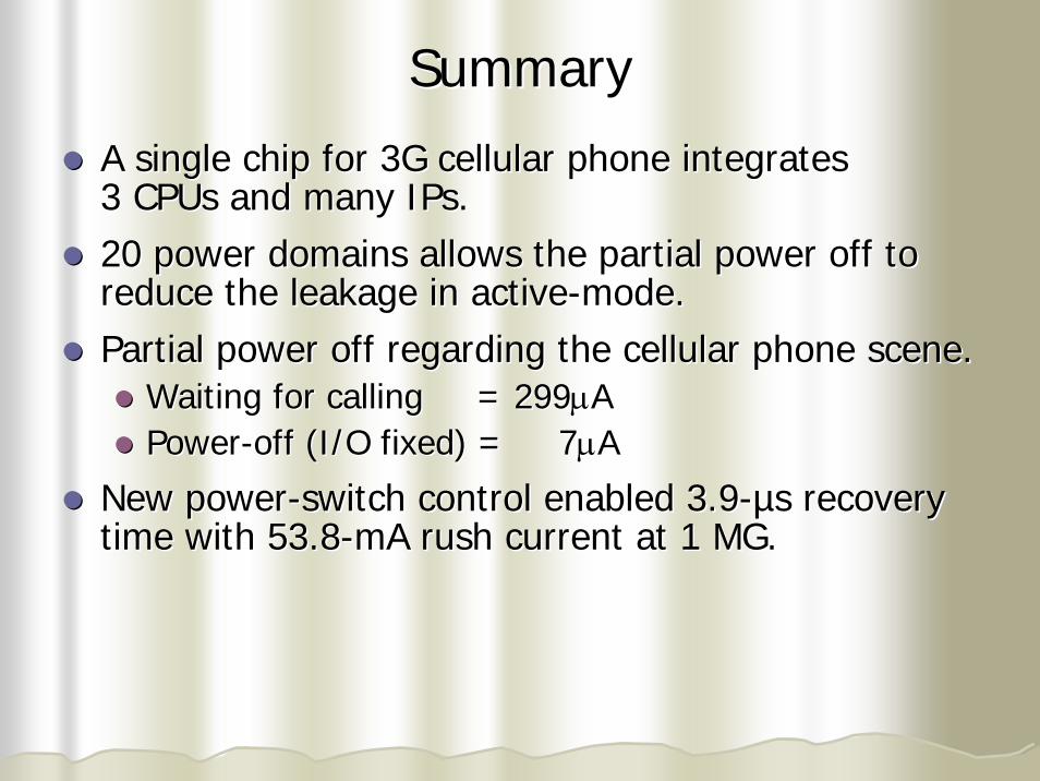
SummarySummary
A single chip for 3G cellular phone integrates A single chip for 3G cellular phone integrates 3 CPUs and many 3 CPUs and many IPsIPs. . 20 power domains allows the partial power off to 20 power domains allows the partial power off to reduce the leakage in activereduce the leakage in active--mode.mode.Partial power off regarding the cellular phone scene.Partial power off regarding the cellular phone scene.
Waiting for calling = 299Waiting for calling = 299μμAAPowerPower--off (I/O fixed) = 7off (I/O fixed) = 7μμAA
New powerNew power--switch control enabled 3.9switch control enabled 3.9--µµs recovery s recovery time with 53.8time with 53.8--mA rush current at 1 MG.mA rush current at 1 MG.