Embed Size (px)
Citation preview
8/16-bitXMEGA A1 Microcontroller
ATxmega384A1ATxmega256A1ATxmega192A1ATxmega128A1ATxmega64A1
Preliminary
8067D–AVR–08/08
Features• High-performance, Low-power 8/16-bit AVR XMEGA Microcontroller• Non-Volatile Program and Data Memories
– 64K - 384K Bytes of In-System Self-Programmable Flash– 4K - 8K Bytes Boot Section with Independent Lock Bits– 2K - 4K Bytes EEPROM– 4K - 32K Bytes Internal SRAM
External Bus Interface for up to 16M bytes SRAMExternal Bus Interface for up to 128M bit SDRAM
• Peripheral Features– Four-channel DMA Controller with support for external requests– Eight-channel Event System– Eight 16-bit Timer/Counters
Four Timer/Counters with 4 Output Compare or Input Capture channelsFour Timer/Counters with 2 Output Compare or Input Capture channelsHigh-Resolution Extension on all Timer/CountersAdvanced Waveform Extension on two Timer/Counters
– Eight USARTsIrDA modulation/demodulation for one USART
– Four Two-Wire Interfaces with dual address match (I2C and SMBus compatible)– Four SPI (Serial Peripheral Interface) peripherals– AES and DES Crypto Engine– 16-bit Real Time Counter with separate Oscillator– Two Eight-channel, 12-bit, 2 Msps Analog to Digital Converters– Two Two-channel, 12-bit, 1 Msps Digital to Analog Converters– Four Analog Comparators with Window compare function– External Interrupts on all General Purpose I/O pins– Programmable Watchdog Timer with Separate On-chip Ultra Low Power Oscillator
• Special Microcontroller Features– Power-on Reset and Programmable Brown-out Detection– Internal and External Clock Options with PLL and Prescaler– Programmable Multi-level Interrupt Controller– Sleep Modes: Idle, Power-down, Standby, Power-save, Extended Standby– Advanced Programming, Test and Debugging Interfaces
JTAG (IEEE 1149.1 Compliant) Interface for programming, test and debuggingPDI (Program and Debug Interface) for programming and debugging
• I/O and Packages– 78 Programmable I/O Lines– 100 - lead TQFP– 100 - ball CBGA
• Operating Voltage– 1.6 – 3.6V
• Speed performance– 0 – 12 MHz @ 1.6 – 3.6V– 0 – 32 MHz @ 2.7 – 3.6V
Typical Applications • Industrial control • Climate control • Hand-held battery applications• Factory automation • ZigBee • Power tools• Building control • Motor control • HVAC• Board control • Networking • Metering• White Goods • Optical • Medical Applications
XMEGA A1
‘
1. Ordering Information
Notes: 1. This device can also be supplied in wafer form. Please contact your local Atmel sales office for detailed ordering information.2. Pb-free packaging, complies to the European Directive for Restriction of Hazardous Substances (RoHS directive). Also Halide free and fully Green.3. For packaging information, see “Packaging information” on page 63.
2. Pinout/Block Diagram
Figure 2-1. Block diagram and TQFP-pinout.
Note: For full details on pinout and pin functions refer to “Pinout and Pin Functions” on page 48.
Ordering Code Flash (B) E2 (B) SRAM (B) Speed (MHz) Power Supply Package(1)(2)(3) Temp
ATxmega384A1-AU 384K + 8K 4K 32K 32 1.6 - 3.6V
100A
-40° - 85°C
ATxmega256A1-AU 256K + 8K 4K 16K 32 1.6 - 3.6V
ATxmega192A1-AU 192K + 8K 2K 16K 32 1.6 - 3.6V
ATxmega128A1-AU 128K + 8K 2K 8K 32 1.6 - 3.6V
ATxmega64A1-AU 64K + 4K 2K 4K 32 1.6 - 3.6V
ATxmega384A1-CU 384K + 8K 4K 32K 32 1.6 - 3.6V
100C1
ATxmega256A1-CU 256K + 8K 4K 16K 32 1.6 - 3.6V
ATxmega192A1-CU 192K + 8K 2K 16K 32 1.6 - 3.6V
ATxmega128A1-CU 128K + 8K 2K 8K 32 1.6 - 3.6V
ATxmega64A1-CU 64K + 4K 2K 4K 32 1.6 - 3.6V
Package Type
100A 100-lead, 14 x 14 x 1.0 mm, 0.5 mm Lead Pitch, Thin Profile Plastic Quad Flat Package (TQFP)
100C1 100-ball, 9 x 9 x 1.2 mm Body, Ball Pitch 0.88 mm, Chip Ball Grid Array (CBGA)
INDEX CORNER
PA6PA7
GNDAVCC
PB0PB1PB2PB3PB4PB5PB6PB7
GNDVCCPC0PC1PC2PC3PC4PC5PC6PC7
GNDVCCPD0
26 27 28 29 30 31 32 33 34 35 36 37 38 39 40 41 42 43 44 45 46 47 48 49 50
100 99 98 97 96 95 94 93 92 91 90 89 88 87 86 85 84 83 82 81 80 79 78 77 76
75747372717069686766656463626160595857565554535251
12345678910111213141516171819202122232425
PD1
PD2
PD3
PD4
PD5
PD6
PD7
GN
DVC
CPE
0PE
1PE
2PE
3PE
4PE
5PE
6PE
7G
ND
VCC
PF0
PF1
PF2
PF3
PF4
PF5
PK0VCCGNDPJ7PJ6PJ5PJ4PJ3PJ2PJ1PJ0VCCGNDPH7PH6PH5PH4PH3PH2PH1PH0VCCGNDPF7PF6
PA5
PA4
PA3
PA2
PA1
PA0
AVCC
GN
DPR
1PR
0RE
SET/
PDI
PDI
PQ3
PQ2
PQ1
PQ0
GN
DVC
CPK
7PK
6PK
5PK
4PK
3PK
2PK
1
FLASH
RAM
E 2PROMDMA
Interrupt Controlle r
OCD
Exte
rnal
Bus
I nte
rfac
e
ADC A
ADC B
DAC B
DAC A
AC A0
AC A1
AC B0
AC B1
Port
APo
rt B
Event System ctrl
Port K
Port J
Port H
Port QPort R
PowerContro l
ResetContro l
Watchdog
OSC/CLKContro l
BOD POR
RTC
EVENT ROUTING NETWORK
DATA BU S
DATA BU S
VREF
TEMP
Port C
CPU
T/C
0:1
US
AR
T0
:1
TW
I
SP
I
Port FPort EPort D
T/C
0:1
US
AR
T0
/1
TW
I
SP
I
T/C
0:1
US
AR
T0
:1
TW
I
SP
I
T/C
0:1
US
AR
T0
:1
TW
I
SP
I
28067D–AVR–08/08
XMEGA A1
Figure 2-2. CBGA-pinout
A
B
C
D
E
F
G
H
J
K
1 2 3 4 5 6 7 8 9 10
A
B
C
D
E
F
G
H
J
K
10 9 8 7 6 5 4 3 2 1Top view Bottom view
Table 2-1. CBGA-pinout
1 2 3 4 5 6 7 8 9 10
A PK0 VCC GND PJ3 VCC GND PH1 GND VCC PF7
B PK3 PK2 PK1 PJ4 PH7 PH4 PH2 PH0 PF6 PF5
C VCC PK5 PK4 PJ5 PJ0 PH5 PH3 PF2 PF3 VCC
D GND PK6 PK7 PJ6 PJ1 PH6 PF0 PF1 PF4 GND
ETOSC1/
PQ0TOSC2/
PQ1PQ2 PJ7 PJ2 PE7 PE6 PE5 PE4 PE3
FXTAL1/
PR1XTAL2/
PR0RESET/PDI_CLK
PDI_DATA PQ3 PC2 PE2 PE1 PE0 VCC
G GND PA1 PA4 PB3 PB4 PC1 PC6 PD7 PD6 GND
H AVCC PA2 PA5 PB2 PB5 PC0 PC5 PD5 PD4 PD3
J PA0 PA3 PB0 PB1 PB6 PC3 PC4 PC7 PD2 PD1
K PA6 PA7 GND AVCC PB7 VCC GND VCC GND PD0
38067D–AVR–08/08
XMEGA A1
3. Overview
The XMEGA A1 is a family of low power, high performance and peripheral rich CMOS 8/16-bitmicrocontrollers based on the AVR® enhanced RISC architecture. By executing powerfulinstructions in a single clock cycle, the XMEGA A1 achieves throughputs approaching 1 MillionInstructions Per Second (MIPS) per MHz allowing the system designer to optimize power con-sumption versus processing speed.
The AVR CPU combines a rich instruction set with 32 general purpose working registers. All the32 registers are directly connected to the Arithmetic Logic Unit (ALU), allowing two independentregisters to be accessed in one single instruction, executed in one clock cycle. The resultingarchitecture is more code efficient while achieving throughputs many times faster than conven-tional single-accumulator or CISC based microcontrollers.
The XMEGA A1 devices provides the following features: In-System Programmable Flash withRead-While-Write capabilities, Internal EEPROM and SRAM, four-channel DMA Controller,eight-channel Event System, Programmable Multi-level Interrupt Controller, 78 general purposeI/O lines, 16-bit Real Time Counter (RTC), eight flexible 16-bit Timer/Counters with comparemodes and PWM, eight USARTs, four Two Wire Serial Interfaces (TWIs), four Serial PeripheralInterfaces (SPIs), AES and DES crypto engine, two 8-channel, 12-bit ADCs with optional differ-ential input with programmable gain, two 2-channel, 12-bit DACs, four analog comparators withwindow mode, programmable Watchdog Timer with seperate Internal Oscillator, accurate inter-nal oscillators with PLL and prescaler and programmable Brown-Out Detection.
The Program and Debug Interface (PDI), a fast 2-pin interface for programming and debugging,is available. The devices also have an IEEE std. 1149.1 compliant JTAG test interface, and thiscan also be used for On-chip Debug and programming.
The XMEGA A1 devices have five software selectable power saving modes. The Idle modestops the CPU while allowing the SRAM, DMA Controller, Event System, Interrupt Controller andall peripherals to continue functioning. The Power-down mode saves the SRAM and registercontents but stops the oscillators, disabling all other functions until the next TWI or pin-changeinterrupt, or Reset. In Power-save mode, the asynchronous Real Time Counter continues to run,allowing the application to maintain a timer base while the rest of the device is sleeping. InStandby mode, the Crystal/Resonator Oscillator is kept running while the rest of the device issleeping. This allows very fast start-up from external crystal combined with low power consump-tion. In Extended Standby mode, both the main Oscillator and the Asynchronous Timer continueto run. To further reduce power consumption, the peripheral clock to each individual peripheralcan optionally be stopped in Active mode and Idle sleep mode.
The device is manufactured using Atmel's high-density nonvolatile memory technology. The pro-gram Flash memory can be reprogrammed in-system through the PDI or JTAG. A Bootloaderrunning in the device can use any interface to download the application program to the Flashmemory. The Bootloader software in the Boot Flash section will continue to run while the Appli-cation Flash section is updated, providing true Read-While-Write operation. By combining an8/16-bit RISC CPU with In-System Self-Programmable Flash, the Atmel XMEGA A1 is a power-ful microcontroller family that provides a highly flexible and cost effective solution for manyembedded applications.
The XMEGA A1 devices is supported with a full suite of program and system development toolsincluding: C compilers, macro assemblers, program debugger/simulators, programmers, andevaluation kits.
48067D–AVR–08/08
XMEGA A1
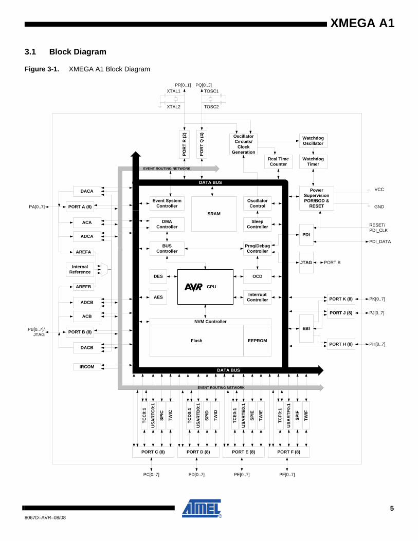
3.1 Block Diagram
Figure 3-1. XMEGA A1 Block Diagram
Power SupervisionPOR/BOD &
RESETPORT A (8)
PORT B (8)
EVENT ROUTING NETWORK
EVENT ROUTING NETWORK
DMAController
BUS Controller
SRAM
EBI
ADCA
DACA
ACA
DACB
ADCB
ACB
OCD
Internal Reference
PORT K (8)
PORT J (8)
PORT H (8)
PDI
CPU
PH[0..7]
PJ[0..7]
PK[0..7]
PA[0..7]
PB[0..7]/JTAG
Watchdog Timer
WatchdogOscillator
Interrupt Controller
DATA BUS
DATA BUS
Prog/DebugController
VCC
GND
Oscillator Circuits/
Clock Generation
Oscillator Control
Real TimeCounter
Event System Controller
JTAG
AREFA
AREFB
PDI_DATA
RESET/PDI_CLK
PORT B
Sleep Controller
Flash EEPROM
NVM Controller
DES
AES
IRCOM
PORT C (8)
PC[0..7]
TCC
0:1
USA
RTC
0:1
TWIC
SPIC
PD[0..7] PE[0..7] PF[0..7]
POR
T R
(2)
XTAL1
XTAL2
PR[0..1]TOSC1
TOSC2
PQ[0..3]
POR
T Q
(4)
PORT D (8)
TCD
0:1
USA
RTD
0:1
TWID
SPID
TCF0
:1
USA
RTF
0:1
TWIF
SPIF
TCE0
:1
USA
RTE
0:1
TWIE
SPIE
PORT E (8) PORT F (8)
58067D–AVR–08/08
XMEGA A1
4. Resources
A comprehensive set of development tools, application notes and datasheets are available fordownload on http://www.atmel.com/avr.
4.1 Recommended reading
• XMEGA A Manual
• XMEGA A Application Notes
This device data sheet only contains part specific information and a short description of eachperipheral and module. The XMEGA A Manual describes the modules and peripherals in depth.The XMEGA A application notes contain example code and show applied use of the modulesand peripherals.
The XMEGA A Manual and Application Notes are available from http://www.atmel.com/avr.
5. Disclaimer
For devices that are not available yet, typical values contained in this datasheet are based onsimulations and characterization of other AVR XMEGA microcontrollers manufactured on thesame process technology. Min. and Max values will be available after the device ischaracterized.
68067D–AVR–08/08
XMEGA A1
6. AVR CPU
6.1 Features
• 8/16-bit high performance AVR RISC Architecture– 138 instructions– Hardware multiplier
• 32x8-bit registers directly connected to the ALU• Stack in SRAM• Stack Pointer accessible in I/O memory space• Direct addressing of up to 16M Bytes of program and data memory• True 16/24-bit access to 16/24-bit I/O registers• Support for 8-, 16- and 32-bit Arithmetic• Configuration Change Protection of system critical features
6.2 Overview
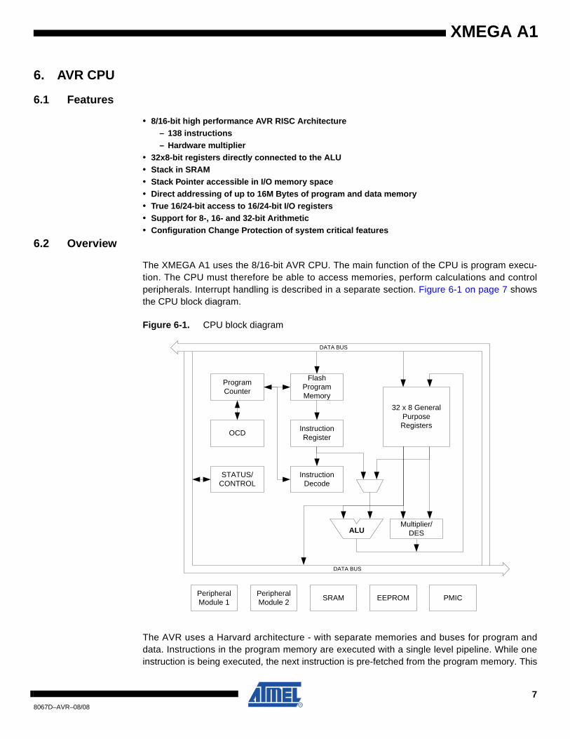
The XMEGA A1 uses the 8/16-bit AVR CPU. The main function of the CPU is program execu-tion. The CPU must therefore be able to access memories, perform calculations and controlperipherals. Interrupt handling is described in a separate section. Figure 6-1 on page 7 showsthe CPU block diagram.
Figure 6-1. CPU block diagram
The AVR uses a Harvard architecture - with separate memories and buses for program anddata. Instructions in the program memory are executed with a single level pipeline. While oneinstruction is being executed, the next instruction is pre-fetched from the program memory. This
Flash Program Memory
InstructionDecode
Program Counter
OCD
32 x 8 General Purpose Registers
ALUMultiplier/
DES
InstructionRegister
STATUS/CONTROL
Peripheral Module 1
Peripheral Module 2 EEPROM PMICSRAM
DATA BUS
DATA BUS
78067D–AVR–08/08
XMEGA A1
concept enables instructions to be executed in every clock cycle. The program memory is In-System Self-Programmable Flash memory.
6.3 Register File
The fast-access Register File contains 32 x 8-bit general purpose working registers with singleclock cycle access time. This allows single-cycle Arithmetic Logic Unit (ALU) operation. In a typ-ical ALU cycle, the operation is performed on two Register File operands, and the result is storedback in the Register File.
Six of the 32 registers can be used as three 16-bit address register pointers for data spaceaddressing - enabling efficient address calculations. One of these address pointers can also beused as an address pointer for look up tables in Flash program memory.
6.4 ALU - Arithmetic Logic Unit
The high performance Arithmetic Logic Unit (ALU) supports arithmetic and logic operationsbetween registers or between a constant and a register. Single register operations can also beexecuted. Within a single clock cycle, arithmetic operations between general purpose registersor between a register and an immediate are executed. After an arithmetic or logic operation, theStatus Register is updated to reflect information about the result of the operation.
The ALU operations are divided into three main categories – arithmetic, logical, and bit-func-tions. Both 8- and 16-bit arithmetic is supported, and the instruction set allows for efficientimplementation of 32-bit aritmetic. The ALU also provides a powerful multiplier supporting bothsigned and unsigned multiplication and fractional format.
6.5 Program Flow
When the device is powered on, the CPU starts to execute instructions from the lowest addressin the Flash Program Memory ‘0’. The Program Counter (PC) addresses the next instruction tobe fetched. After a reset, the PC is set to location ‘0’.
Program flow is provided by conditional and unconditional jump and call instructions, capable ofaddressing the whole address space directly. Most AVR instructions use a 16-bit word format,while a limited number uses a 32-bit format.
During interrupts and subroutine calls, the return address PC is stored on the Stack. The Stackis effectively allocated in the general data SRAM, and consequently the Stack size is only limitedby the total SRAM size and the usage of the SRAM. After reset the Stack Pointer (SP) points tothe highest address in the internal SRAM. The SP is read/write accessible in the I/O memoryspace, enabling easy implementation of multiple stacks or stack areas. The data SRAM caneasily be accessed through the five different addressing modes supported in the AVR CPU.
88067D–AVR–08/08
XMEGA A1
7. Memories
7.1 Features
• Flash Program Memory– One linear address space– In-System Programmable– Self-Programming and Bootloader support– Application Section for application code– Application Table Section for application code or data storage– Boot Section for application code or bootloader code– Separate lock bits and protection for all sections
• Data Memory– One linear address space– Single cycle access from CPU– SRAM– EEPROM
Byte or page accessibleOptional memory mapping for direct load and store
– I/O MemoryConfiguration and Status registers for all peripherals and modules16-bit accessible General Purpose Register for global variables or flags
– External Memory support– Bus arbitration
Safe and deterministic handling of CPU and DMA Controller priority– Separate buses for SRAM, EEPROM, I/O Memory and External Memory access
Simultaneous bus access for CPU and DMA Controller• Calibration Row Memory for factory programmed data
Oscillator calibration bytesSerial numberDevice ID for each device type
• User Signature RowOne flash page in sizeCan be read and written from softwareData is kept after Chip Erase
7.2 Overview
The AVR architecture has two main memory spaces, the Program Memory and the Data Mem-ory. In addition, the XMEGA A1 features an EEPROM Memory for non-volatile data storage. Allthree memory spaces are linear and require no paging. The available memory size configura-tions are shown in “Ordering Information” on page 2. In addition each device has a Flashmemory signature row for calibration data, device identification, serial number etc.
Non-volatile memory spaces can be locked for further write or read/write operations. This pre-vents unrestricted access to the application software.
7.3 In-System Programmable Flash Program Memory
The XMEGA A1 devices contains On-chip In-System Programmable Flash memory for programstorage, see Figure 7-1 on page 10. Since all AVR instructions are 16- or 32-bits wide, eachFlash address location is 16 bits.
98067D–AVR–08/08
XMEGA A1
The Program Flash memory space is divided into Application and Boot sections. Both sectionshave dedicated Lock Bits for setting restrictions on write or read/write operations. The Store Pro-gram Memory (SPM) instruction must reside in the Boot Section when used to write to the Flashmemory.
A third section inside the Application section is referred to as the Application Table section whichhas separate Lock bits for storage of write or read/write protection. The Application Table sec-tion can be used for storing non-volatile data or application software.
The Application Table Section and Boot Section can also be used for general applicationsoftware.
7.4 Data Memory
The Data Memory consist of the I/O Memory, EEPROM and SRAM memories, all within one lin-ear address space, see Figure 7-2 on page 10. To simplify development, the memory map for alldevices in the family is identical and with empty, reserved memory space for smaller devices.
Figure 7-1. Flash Program Memory (Hexadecimal address)
Word Address
0 Application Section
(384K/256K/192K/128K/64K)
...
2EFFF / 1EFFF / 16FFF / EFFF / 77FF
2F000 / 1F000 / 17000 / F000 / 7800 Application Table Section
(8K/8K/8K/8K/4K)2FFFF / 1FFFF / 17FFF / FFFF / 7FFF
30000 / 20000 / 18000 / 10000 / 8000 Boot Section
(8K/8K/8K/8K/4K)30FFF / 20FFF / 18FFF / 10FFF / 87FF
Figure 7-2. Data Memory Map (Hexadecimal address)
Byte Address ATxmega192A1 Byte Address ATxmega128A1 Byte Address ATxmega64A1
0 I/O Registers
(4KB)
0 I/O Registers
(4KB)
0 I/O Registers
(4KB)FFF FFF FFF
1000 EEPROM(2K)
1000 EEPROM(2K)
1000 EEPROM(2K)17FF 17FF 17FF
RESERVED RESERVED RESERVED
2000 Internal SRAM(16K)
2000 Internal SRAM(8K)
2000 Internal SRAM(4K)5FFF 3FFF 2FFF
6000 External Memory(0 to 16 MB)
4000 External Memory(0 to 16 MB)
3000 External Memory(0 to 16 MB)FFFFFF FFFFFF FFFFFF
108067D–AVR–08/08
XMEGA A1
7.4.1 I/O Memory
All peripherals and modules are addressable through I/O memory locations in the data memoryspace. All I/O memory locations can be accessed by the Load (LD/LDS/LDD) and Store(ST/STS/STD) instructions, transferring data between the 32 general purpose registers in theCPU and the I/O Memory.
The IN and OUT instructions can address I/O memory locations in the range 0x00 - 0x3Fdirectly.
I/O registers within the address range 0x00 - 0x1F are directly bit-accessible using the SBI andCBI instructions. The value of single bits can be checked by using the SBIS and SBIC instruc-tions on these registers.
The I/O memory address for all peripherals and modules in XMEGA A1 is shown in the “Periph-eral Module Address Map” on page 54.
7.4.2 SRAM Data Memory
The XMEGA A1 devices has internal SRAM memory for data storage.
7.4.3 EEPROM Data Memory
The XMEGA A1 devices has internal EEPROM memory for non-volatile data storage. It isaddressable either in a separate data space or it can be memory mapped into the normal datamemory space. The EEPROM memory supports both byte and page access.
Byte Address ATxmega384A1 Byte Address ATxmega256A1
0 I/O Registers
(4KB)
0 I/O Registers
(4KB)FFF FFF
1000EEPROM
(4K)
1000EEPROM
(4K)1FFF 1FFF
2000 Internal SRAM
(32K)
2000 Internal SRAM
(16K)9FFF 5FFF
10000 External Memory
(0 to 16 MB)
6000 External Memory
(0 to 16 MB)FFFFFF FFFFFF
118067D–AVR–08/08
XMEGA A1
7.4.4 EBI - External Bus Interface
• Supports SRAM up to– 512K Bytes using 2-port EBI– 16M Bytes using 3-port EBI
• Supports SDRAM up to– 128M bit using 3-port EBI
• Four software configurable Chip Selects• Software configurable Wait State insertion• Clocked from the Peripheral 2x Clock at up to two times the CPU clock speed
The External Bus Interface (EBI) is the interface for connecting external peripheral and memoryto the data memory space. The XMEGA A1 has 3 ports that can be used for the EBI. It can inter-face external SRAM, SDRAM, and/or peripherals such as LCD displays and other memorymapped devices.
The address space, and the number of pins used, for the external memory is selectable from256 bytes (8-bit) and up to 16M bytes (24-bit). Various multiplexing modes for address and datalines can be selected for optimal use of pins when more or less pins is available for the EBI.
Each of the four chip selects has seperate configuration, and can be configured for SRAM,SRAM Low Pin Count (LPC) or SDRAM. The data memory address space associated for eachchip select is decided by a configurable base address and address size for each chip celect.
For SDRAM both 4-bit SDRAM is supported, and SDRAM configurations such as CAS Latencyand Refresh rate is configurable in software.
The EBI is clocked from the Peripheral 2x Clock, running up to two times faster than the CPUand supporting speeds of up to 64 MHz.
128067D–AVR–08/08
XMEGA A1
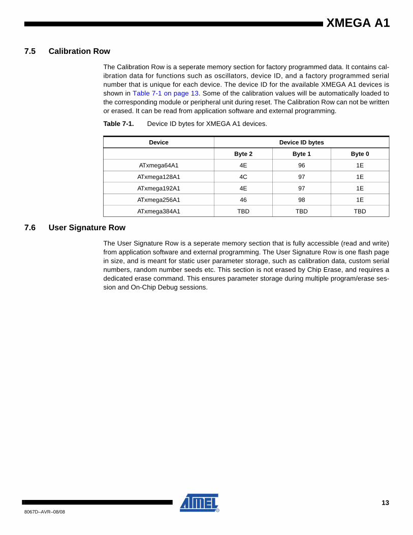
7.5 Calibration Row
The Calibration Row is a seperate memory section for factory programmed data. It contains cal-ibration data for functions such as oscillators, device ID, and a factory programmed serialnumber that is unique for each device. The device ID for the available XMEGA A1 devices isshown in Table 7-1 on page 13. Some of the calibration values will be automatically loaded tothe corresponding module or peripheral unit during reset. The Calibration Row can not be writtenor erased. It can be read from application software and external programming.
Table 7-1. Device ID bytes for XMEGA A1 devices.
7.6 User Signature Row
The User Signature Row is a seperate memory section that is fully accessible (read and write)from application software and external programming. The User Signature Row is one flash pagein size, and is meant for static user parameter storage, such as calibration data, custom serialnumbers, random number seeds etc. This section is not erased by Chip Erase, and requires adedicated erase command. This ensures parameter storage during multiple program/erase ses-sion and On-Chip Debug sessions.
Device Device ID bytes
Byte 2 Byte 1 Byte 0
ATxmega64A1 4E 96 1E
ATxmega128A1 4C 97 1E
ATxmega192A1 4E 97 1E
ATxmega256A1 46 98 1E
ATxmega384A1 TBD TBD TBD
138067D–AVR–08/08
XMEGA A1
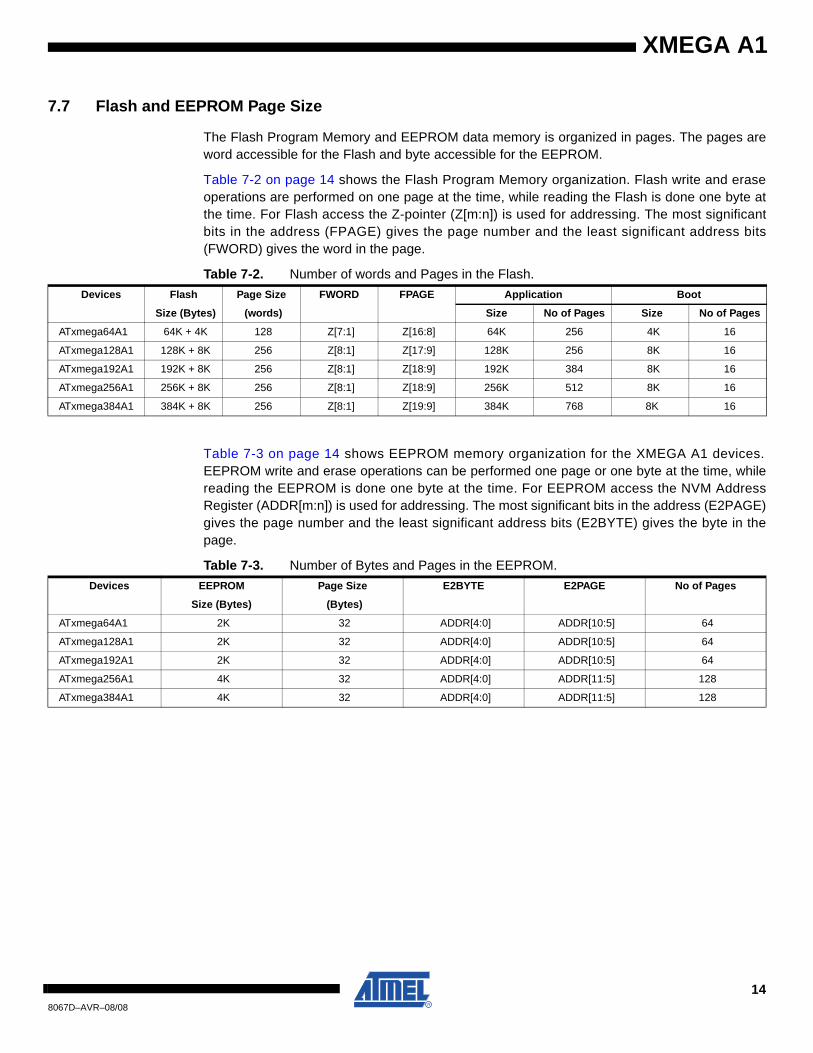
7.7 Flash and EEPROM Page Size
The Flash Program Memory and EEPROM data memory is organized in pages. The pages areword accessible for the Flash and byte accessible for the EEPROM.
Table 7-2 on page 14 shows the Flash Program Memory organization. Flash write and eraseoperations are performed on one page at the time, while reading the Flash is done one byte atthe time. For Flash access the Z-pointer (Z[m:n]) is used for addressing. The most significantbits in the address (FPAGE) gives the page number and the least significant address bits(FWORD) gives the word in the page.
Table 7-2. Number of words and Pages in the Flash.
Table 7-3 on page 14 shows EEPROM memory organization for the XMEGA A1 devices.EEPROM write and erase operations can be performed one page or one byte at the time, whilereading the EEPROM is done one byte at the time. For EEPROM access the NVM AddressRegister (ADDR[m:n]) is used for addressing. The most significant bits in the address (E2PAGE)gives the page number and the least significant address bits (E2BYTE) gives the byte in thepage.
Table 7-3. Number of Bytes and Pages in the EEPROM.
Devices Flash Page Size FWORD FPAGE Application Boot
Size (Bytes) (words) Size No of Pages Size No of Pages
ATxmega64A1 64K + 4K 128 Z[7:1] Z[16:8] 64K 256 4K 16
ATxmega128A1 128K + 8K 256 Z[8:1] Z[17:9] 128K 256 8K 16
ATxmega192A1 192K + 8K 256 Z[8:1] Z[18:9] 192K 384 8K 16
ATxmega256A1 256K + 8K 256 Z[8:1] Z[18:9] 256K 512 8K 16
ATxmega384A1 384K + 8K 256 Z[8:1] Z[19:9] 384K 768 8K 16
Devices EEPROM Page Size E2BYTE E2PAGE No of Pages
Size (Bytes) (Bytes)
ATxmega64A1 2K 32 ADDR[4:0] ADDR[10:5] 64
ATxmega128A1 2K 32 ADDR[4:0] ADDR[10:5] 64
ATxmega192A1 2K 32 ADDR[4:0] ADDR[10:5] 64
ATxmega256A1 4K 32 ADDR[4:0] ADDR[11:5] 128
ATxmega384A1 4K 32 ADDR[4:0] ADDR[11:5] 128
148067D–AVR–08/08

XMEGA A1
8. DMAC - Direct Memory Access Controller
8.1 Features
• Allows High-speed data transfer– From memory to peripheral– From memory to memory– From peripheral to memory– From peripheral to peripheral
• 4 Channels• From 1 byte and up to 16M bytes transfers in a single transaction• Multiple addressing modes for source and destination address
– Increment– Decrement– Static
• 1, 2, 4, or 8 byte Burst Transfers• Programmable priority between channels
8.2 Overview
The XMEGA A1 has a Direct Memory Access (DMA) Controller to move data between memoriesand peripherals in the data space. The DMA controller uses the same data bus as the CPU totransfer data.
It has 4 channels that can be configured independently. Each DMA channel can perform datatransfers in blocks of configurable size from 1 to 64K bytes. A repeat counter can be used torepeat each block transfer for single transactions up to 16M bytes. Each DMA channel can beconfigured to access the source and destination memory address with incrementing, decrement-ing or static addressing. The addressing is independent for source and destination address.When the transaction is complete the original source and destination address can automaticallybe reloaded to be ready for the next transaction.
The DMAC can access all the peripherals through their I/O memory registers, and the DMA maybe used for automatic transfer of data to/from communication modules, as well as automaticdata retrieval from ADC conversions, data transfer to DAC conversions, or data transfer to orfrom port pins. A wide range of transfer triggers is available from the peripherals, Event Systemand software. Each DMA channel has different transfer triggers.
To allow for continuous transfers, two channels can be interlinked so that the second takes overthe transfer when the first is finished and vice versa.
The DMA controller can read from memory mapped EEPROM, but it cannot write to theEEPROM or access the Flash.
158067D–AVR–08/08
XMEGA A1
9. Event System
9.1 Features
• Inter-peripheral communication and signalling with minimum latency• CPU and DMA independent operation• 8 Event Channels allows for up to 8 signals to be routed at the same time• Events can be generated by
– Timer/Counters (TCxn)– Real Time Counter (RTC)– Analog to Digital Converters (ADCx)– Analog Comparators (ACx)– Ports (PORTx)– System Clock (ClkSYS)– Software (CPU)
• Events can be used by– Timer/Counters (TCxn)– Analog to Digital Converters (ADCx)– Digital to Analog Converters (DACx)– Ports (PORTx)– DMA Controller (DMAC)– IR Communication Module (IRCOM)
• The same event can be used by multiple peripherals for synchronized timing• Advanced Features
– Manual Event Generation from software (CPU)– Quadrature Decoding– Digital Filtering
• Functions in Active and Idle mode
9.2 Overview
The Event System is a set of features for inter-peripheral communication. It enables the possibil-ity for a change of state in one peripheral to automatically trigger actions in one or moreperipherals. What changes in a peripheral that will trigger actions in other peripherals are config-urable by software. It is a simple, but powerful system as it allows for autonomous control ofperipherals without any use of interrupts, CPU or DMA resources.
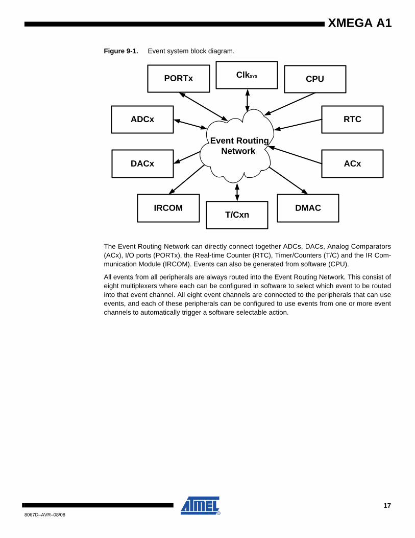
The indication of a change in a peripheral is referred to as an event, and is usually the same asthe interrupt conditions for that peripheral. Events are passed between peripherals using a dedi-cated routing network called the Event Routing Network. Figure 9-1 on page 17 shows a basicblock diagram of the Event System with the Event Routing Network and the peripherals to whichit is connected. This highly flexible system can be used for simple routing of signals, pin func-tions or for sequencing of events.
The maximum latency is two CPU clock cycles from when an event is generated in one periph-eral, until the actions are triggered in one or more other peripherals.
The Event System is functional in both Active and Idle modes.
168067D–AVR–08/08
XMEGA A1
Figure 9-1. Event system block diagram.
The Event Routing Network can directly connect together ADCs, DACs, Analog Comparators(ACx), I/O ports (PORTx), the Real-time Counter (RTC), Timer/Counters (T/C) and the IR Com-munication Module (IRCOM). Events can also be generated from software (CPU).
All events from all peripherals are always routed into the Event Routing Network. This consist ofeight multiplexers where each can be configured in software to select which event to be routedinto that event channel. All eight event channels are connected to the peripherals that can useevents, and each of these peripherals can be configured to use events from one or more eventchannels to automatically trigger a software selectable action.
ADCx
DACx
Event Routing Network
PORTx CPU
ACx
RTC
T/CxnDMACIRCOM
ClkSYS
178067D–AVR–08/08
XMEGA A1
10. System Clock and Clock options
10.1 Features
• Fast start-up time• Safe run-time clock switching• Internal Oscillators:
– 32 MHz run-time calibrated RC oscillator– 2 MHz run-time calibrated RC oscillator – 32 kHz calibrated RC oscillator– 32 kHz Ultra Low Power (ULP) oscillator
• External clock options– 0.4 - 16 MHz Crystal Oscillator– 32 kHz Crystal Oscillator– External clock
• PLL with internal and external clock options with 2 to 31x multiplication• Clock Prescalers with 2 to 2048x division• Fast peripheral clock running at 2 and 4 times the CPU clock speed• Automatic Run-Time Calibration of internal oscillators• Crystal Oscillator failure detection
10.2 Overview
XMEGA A1 has an advanced clock system, supporting a large number of clock sources. It incor-porates both integrated oscillators, external crystal oscillators and resonators. A high frequencyPhase Locked Loop (PLL) and clock prescalers can be controlled from software to generate awide range of clock frequencies from the clock source input.
It is possible to switch between clock sources from software during run-time. After reset thedevice will always start up running from the 2 Mhz internal oscillator.
A calibration feature is available, and can be used for automatic run-time calibration of the inter-nal 2 MHz and 32 MHz oscillators. This reduce frequency drift over voltage and temperature.
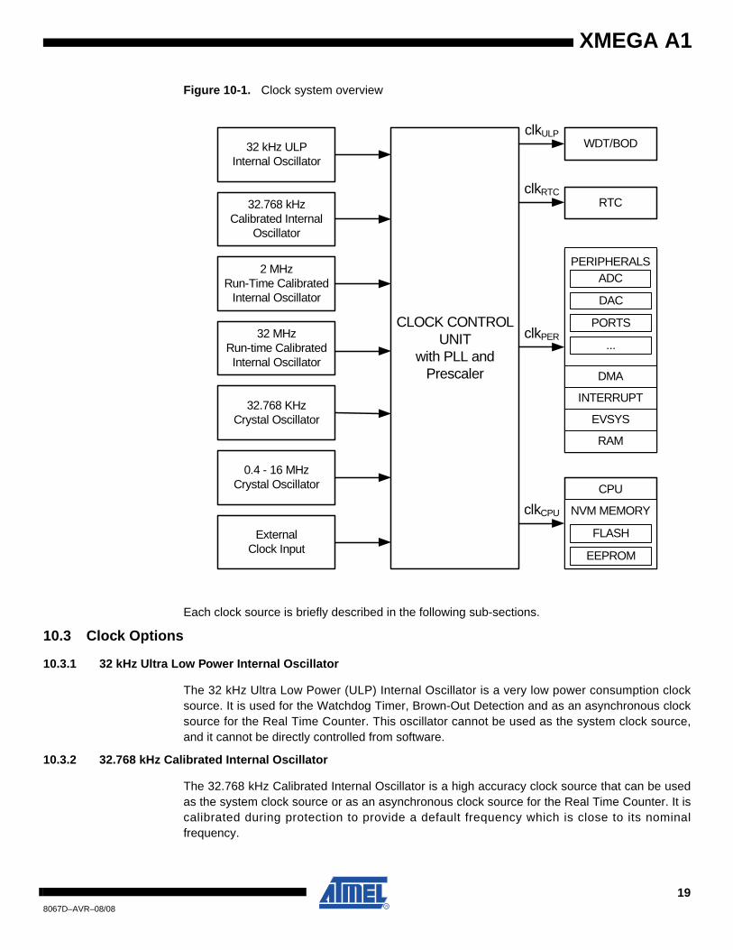
A Crystal Oscillator Failure Monitor can be enabled to issue a Non-Maskable Interrupt andswitch to internal oscillator if the external oscillator fails. Figure 10-1 on page 19 shows the prin-cipal clock system in XMEGA A1.
188067D–AVR–08/08
XMEGA A1
Figure 10-1. Clock system overview
Each clock source is briefly described in the following sub-sections.
10.3 Clock Options
10.3.1 32 kHz Ultra Low Power Internal Oscillator
The 32 kHz Ultra Low Power (ULP) Internal Oscillator is a very low power consumption clocksource. It is used for the Watchdog Timer, Brown-Out Detection and as an asynchronous clocksource for the Real Time Counter. This oscillator cannot be used as the system clock source,and it cannot be directly controlled from software.
10.3.2 32.768 kHz Calibrated Internal Oscillator
The 32.768 kHz Calibrated Internal Oscillator is a high accuracy clock source that can be usedas the system clock source or as an asynchronous clock source for the Real Time Counter. It iscalibrated during protection to provide a default frequency which is close to its nominalfrequency.
32 MHzRun-time CalibratedInternal Oscillator
32 kHz ULPInternal Oscillator
32.768 kHz Calibrated Internal
Oscillator
32.768 KHz Crystal Oscillator
0.4 - 16 MHzCrystal Oscillator
2 MHzRun-Time Calibrated
Internal Oscillator
ExternalClock Input
CLOCK CONTROL UNIT
with PLL and Prescaler
WDT/BODclkULP
RTCclkRTC
EVSYS
PERIPHERALSADC
DAC
PORTS
...clkPER
DMA
INTERRUPT
RAM
NVM MEMORY
FLASH
EEPROM
CPU
clkCPU
198067D–AVR–08/08
XMEGA A1
10.3.3 32.768 kHz Crystal Oscillator
The 32.768 kHz Crystal Oscillator is a low power driver for an external watch crystal. It can beused as system clock source or as asynchronous clock source for the Real Time Counter.
10.3.4 0.4 - 16 MHz Crystal Oscillator
The 0.4 - 16 MHz Crystal Oscillator is a driver intended for driving both external resonators andcrystals ranging from 400 kHz to 16 MHz.
10.3.5 2 MHz Run-time Calibrated Internal Oscillator
The 2 MHz Run-time Calibrated Internal Oscillator is a high frequency oscillator. It is calibratedduring protection to provide a default frequency which is close to its nominal frequency. Theoscillator can use the 32 kHz Calibrated Internal Oscillator or the 32 kHz Crystal Oscillator as asource for calibrating the frequency run-time to compensate for temperature and voltage drifthereby optimizing the accuracy of the oscillator.
10.3.6 32 MHz Run-time Calibrated Internal Oscillator
The 32 MHz Run-time Calibrated Internal Oscillator is a high frequency oscillator. It is calibratedduring protection to provide a default frequency which is close to its nominal frequency. Theoscillator can use the 32 kHz Calibrated Internal Oscillator or the 32 kHz Crystal Oscillator as asource for calibrating the frequency run-time to compensate for temperature and voltage drifthereby optimizing the accuracy of the oscillator.
10.3.7 External Clock input
The external clock input gives the possibility to connect a clock from an external source.
10.3.8 PLL with Multiplication factor 2 - 31x
The PLL provides the possibility of multiplying a frequency by any number from 2 to 31. In com-bination with the prescalers, this gives a wide range of output frequencies from all clock sources.
208067D–AVR–08/08
XMEGA A1
11. Power Management and Sleep Modes
11.1 Features
• 5 sleep modes– Idle– Power-down– Power-save– Standby– Extended standby
• Power Reduction registers to disable clocks to unused peripherals
11.2 Overview
The XMEGA A1 provides various sleep modes tailored to reduce power consumption to a mini-mum. All sleep modes are available and can be entered from Active mode. In Active mode theCPU is executing application code. The application code decides when and what sleep mode toenter. Interrupts from enabled peripherals and all enabled reset sources can restore the micro-controller from sleep to Active mode.
In addition, Power Reduction registers provide a method to stop the clock to individual peripher-als from software. When this is done, the current state of the peripheral is frozen and there is nopower consumption from that peripheral. This reduces the power consumption in Active modeand Idle sleep mode.
11.3 Sleep Modes
11.3.1 Idle Mode
In Idle mode the CPU and Non-Volatile Memory are stopped, but all peripherals including theInterrupt Controller, Event System and DMA Controller are kept running. Interrupt requests fromall enabled interrupts will wake the device.
11.3.2 Power-down Mode
In Power-down mode all system clock sources, and the asynchronous Real Time Counter (RTC)clock source, are stopped. This allows operation of asynchronous modules only. The only inter-rupts that can wake up the MCU are the Two Wire Interface address match interrupts, andasynchronous port interrupts, e.g pin change.
11.3.3 Power-save Mode
Power-save mode is identical to Power-down, with one exception: If the RTC is enabled, it willkeep running during sleep and the device can also wake up from RTC interrupts.
11.3.4 Standby Mode
Standby mode is identical to Power-down with the exception that all enabled system clocksources are kept running, while the CPU, Peripheral and RTC clocks are stopped. This reducesthe wake-up time when external crystals or resonators are used.
11.3.5 Extended Standby Mode
Extended Standby mode is identical to Power-save mode with the exception that all enabledsystem clock sources are kept running while the CPU and Peripheral clocks are stopped. Thisreduces the wake-up time when external crystals or resonators are used.
218067D–AVR–08/08
XMEGA A1
12. System Control and Reset
12.1 Features
• Multiple reset sources for safe operation and device reset– Power-On Reset – External Reset– Watchdog Reset
The Watchdog Timer runs from separate, dedicated oscillator– Brown-Out Reset
Accurate, programmable Brown-Out levels– JTAG Reset– PDI reset– Software reset
• Asynchronous reset– No running clock in the device is required for reset
• Reset status register
12.2 Resetting the AVR
During reset, all I/O registers are set to their initial values. The SRAM content is not reset. Appli-cation execution starts from the Reset Vector. The instruction placed at the Reset Vector shouldbe an Absolute Jump (JMP) instruction to the reset handling routine. By default the Reset Vectoraddress is the lowest Flash program memory address, ‘0’, but it is possible to move the ResetVector to the first address in the Boot Section.
The I/O ports of the AVR are immediately tri-stated when a reset source goes active.
The reset functionality is asynchronous, so no running clock is required to reset the device.
After the device is reset, the reset source can be determined by the application by reading theReset Status Register.
12.3 Reset Sources
12.3.1 Power-On Reset
The MCU is reset when the supply voltage VCC is below the Power-on Reset threshold voltage.
12.3.2 External Reset
The MCU is reset when a low level is present on the RESET pin.
12.3.3 Watchdog Reset
The MCU is reset when the Watchdog Timer period expires and the Watchdog Reset is enabled.The Watchdog Timer runs from a dedicated oscillator independent of the System Clock. Formore details see “WDT - Watchdog Timer” on page 23.
12.3.4 Brown-Out Reset
The MCU is reset when the supply voltage VCC is below the Brown-Out Reset threshold voltageand the Brown-out Detector is enabled. The Brown-out threshold voltage is programmable.
228067D–AVR–08/08
XMEGA A1
12.3.5 JTAG reset
The MCU is reset as long as there is a logic one in the Reset Register in one of the scan chainsof the JTAG system. Refer to IEEE 1149.1 (JTAG) Boundary-scan for details.
12.3.6 PDI reset
The MCU can be reset through the Program and Debug Interface (PDI).
12.3.7 Software reset
The MCU can be reset by the CPU writing to a special I/O register through a timed sequence.
12.4 WDT - Watchdog Timer
12.4.1 Features
• 11 selectable timeout periods, from 8 ms to 8s.• Two operation modes
– Standard mode– Window mode
• Runs from the 1 kHz output of the 32 kHz Ultra Low Power oscillator• Configuration lock to prevent unwanted changes
12.4.2 Overview
The XMEGA A1 has a Watchdog Timer (WDT). The WDT will run continuously when turned onand if the Watchdog Timer is not reset within a software configurable time-out period, the micro-controller will be reset. The Watchdog Reset (WDR) instruction must be run by software to resetthe WDT, and prevent microcontroller reset.
The WDT has a Window mode. In this mode the WDR instruction must be run within a specifiedperiod called a window. Application software can set the minimum and maximum limits for thiswindow. If the WDR instruction is not executed inside the window limits, the microcontroller willbe reset.
A protection mechanism using a timed write sequence is implemented in order to preventunwanted enabling, disabling or change of WDT settings.
For maximum safety, the WDT also has an Always-on mode. This mode is enabled by program-ming a fuse. In Always-on mode, application software can not disable the WDT.
238067D–AVR–08/08
XMEGA A1
13. PMIC - Programmable Multi-level Interrupt Controller
13.1 Features
• Separate interrupt vector for each interrupt• Short, predictable interrupt response time• Programmable Multi-level Interrupt Controller
– 3 programmable interrupt levels– Selectable priority scheme within low level interrupts (round-robin or fixed)– Non-Maskable Interrupts (NMI)
• Interrupt vectors can be moved to the start of the Boot Section
13.2 Overview
XMEGA A1 has a Programmable Multi-level Interrupt Controller (PMIC). All peripherals candefine three different priority levels for interrupts; high, medium or low. Medium level interruptsmay interrupt low level interrupt service routines. High level interrupts may interrupt both low-and medium level interrupt service routines. Low level interrupts have an optional round robinscheme to make sure all interrupts are serviced within a certain amount of time.
The built in oscillator failure detection mechanism can issue a Non-Maskable Interrupt (NMI).
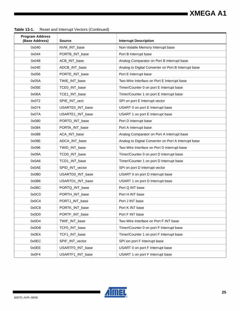
13.3 Interrupt vectors
When an interrupt is serviced, the program counter will jump to the interrupt vector address. Theinterrupt vector is the sum of the peripheral’s base interrupt address and the offset address forspecific interrupts in each peripheral. The base addresses for the XMEGA A1 devices are shownin Table 13-1. Offset addresses for each interrupt available in the peripheral are described foreach peripheral in the XMEGA A manual. For peripherals or modules that have only one inter-rupt, the interrupt vector is shown in Table 13-1. The program address is the word address.
Table 13-1. Reset and Interrupt Vectors
Program Address(Base Address) Source Interrupt Description
0x000 RESET
0x002 OSCF_INT_vect Crystal Oscillator Failure Interrupt vector (NMI)
0x004 PORTC_INT_base Port C Interrupt base
0x008 PORTR_INT_base Port R Interrupt base
0x00C DMA_INT_base DMA Controller Interrupt base
0x014 RTC_INT_base Real Time Counter Interrupt base
0x018 TWIC_INT_base Two-Wire Interface on Port C Interrupt base
0x01C TCC0_INT_base Timer/Counter 0 on port C Interrupt base
0x028 TCC1_INT_base Timer/Counter 1 on port C Interrupt base
0x030 SPIC_INT_vect SPI on port C Interrupt vector
0x032 USARTC0_INT_base USART 0 on port C Interrupt base
0x038 USARTC1_INT_base USART 1 on port C Interrupt base
0x03E AES_INT_vect AES Interrupt vector
248067D–AVR–08/08
XMEGA A1
0x040 NVM_INT_base Non-Volatile Memory Interrupt base
0x044 PORTB_INT_base Port B Interrupt base
0x048 ACB_INT_base Analog Comparator on Port B Interrupt base
0x04E ADCB_INT_base Analog to Digital Converter on Port B Interrupt base
0x056 PORTE_INT_base Port E Interrupt base
0x05A TWIE_INT_base Two-Wire Interface on Port E Interrupt base
0x05E TCE0_INT_base Timer/Counter 0 on port E Interrupt base
0x06A TCE1_INT_base Timer/Counter 1 on port E Interrupt base
0x072 SPIE_INT_vect SPI on port E Interrupt vector
0x074 USARTE0_INT_base USART 0 on port E Interrupt base
0x07A USARTE1_INT_base USART 1 on port E Interrupt base
0x080 PORTD_INT_base Port D Interrupt base
0x084 PORTA_INT_base Port A Interrupt base
0x088 ACA_INT_base Analog Comparator on Port A Interrupt base
0x08E ADCA_INT_base Analog to Digital Converter on Port A Interrupt base
0x096 TWID_INT_base Two-Wire Interface on Port D Interrupt base
0x09A TCD0_INT_base Timer/Counter 0 on port D Interrupt base
0x0A6 TCD1_INT_base Timer/Counter 1 on port D Interrupt base
0x0AE SPID_INT_vector SPI on port D Interrupt vector
0x0B0 USARTD0_INT_base USART 0 on port D Interrupt base
0x0B6 USARTD1_INT_base USART 1 on port D Interrupt base
0x0BC PORTQ_INT_base Port Q INT base
0x0C0 PORTH_INT_base Port H INT base
0x0C4 PORTJ_INT_base Port J INT base
0x0C8 PORTK_INT_base Port K INT base
0x0D0 PORTF_INT_base Port F INT base
0x0D4 TWIF_INT_base Two-Wire Interface on Port F INT base
0x0D8 TCF0_INT_base Timer/Counter 0 on port F Interrupt base
0x0E4 TCF1_INT_base Timer/Counter 1 on port F Interrupt base
0x0EC SPIF_INT_vector SPI ion port F Interrupt base
0x0EE USARTF0_INT_base USART 0 on port F Interrupt base
0x0F4 USARTF1_INT_base USART 1 on port F Interrupt base
Table 13-1. Reset and Interrupt Vectors (Continued)
Program Address(Base Address) Source Interrupt Description
258067D–AVR–08/08
XMEGA A1
14. I/O Ports
14.1 Features
• Selectable input and output configuration for each pin individually• Flexible pin configuration through dedicated Pin Configuration Register• Synchronous and/or asynchronous input sensing with port interrupts and events
– Sense both edges– Sense rising edges– Sense falling edges– Sense low level
• Asynchronous wake-up from all input sensing configurations• Two port interrupts with flexible pin masking• Highly configurable output driver and pull settings:
– Totem-pole– Pull-up/-down– Wired-AND– Wired-OR– Bus-keeper– Inverted I/O
• Optional Slew rate control• Configuration of multiple pins in a single operation• Read-Modify-Write (RMW) support• Toggle/clear/set registers for Output and Direction registers• Clock output on port pin• Event Channel 7 output on port pin• Mapping of port registers (virtual ports) into bit accessible I/O memory space
14.2 Overview
The XMEGA A1 devices have flexible General Purpose I/O Ports. A port consists of up to 8 pins,ranging from pin 0 to pin 7. The ports implement several functions, including synchronous/asyn-chronous input sensing, pin change interrupts and configurable output settings. All functions areindividual per pin, but several pins may be configured in a single operation.
14.3 I/O configuration
All port pins (Pn) have programmable output configuration. In addition, all port pins have aninverted I/O function. For an input, this means inverting the signal between the port pin and thepin register. For an output, this means inverting the output signal between the port register andthe port pin. The inverted I/O function can be used also when the pin is used for alternate func-tions. The port pins also have configurable slew rate limitation to reduce electromagneticemission.
268067D–AVR–08/08
XMEGA A1
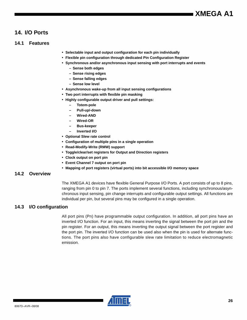
14.3.1 Push-pull
Figure 14-1. I/O configuration - Totem-pole
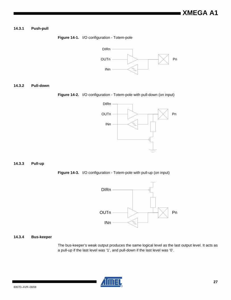
14.3.2 Pull-down
Figure 14-2. I/O configuration - Totem-pole with pull-down (on input)
14.3.3 Pull-up
Figure 14-3. I/O configuration - Totem-pole with pull-up (on input)
14.3.4 Bus-keeper
The bus-keeper’s weak output produces the same logical level as the last output level. It acts asa pull-up if the last level was ‘1’, and pull-down if the last level was ‘0’.
INn
OUTn
DIRn
Pn
INn
OUTn
DIRn
Pn
INn
OUTn
DIRn
Pn
278067D–AVR–08/08
XMEGA A1
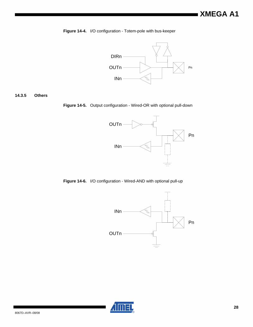
Figure 14-4. I/O configuration - Totem-pole with bus-keeper
14.3.5 Others
Figure 14-5. Output configuration - Wired-OR with optional pull-down
Figure 14-6. I/O configuration - Wired-AND with optional pull-up
INn
OUTn
DIRn
Pn
INn
OUTn
Pn
INn
OUTn
Pn
288067D–AVR–08/08
XMEGA A1
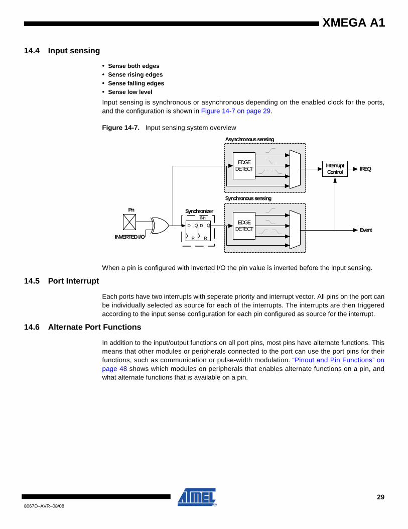
14.4 Input sensing
• Sense both edges• Sense rising edges• Sense falling edges• Sense low level
Input sensing is synchronous or asynchronous depending on the enabled clock for the ports,and the configuration is shown in Figure 14-7 on page 29.
Figure 14-7. Input sensing system overview
When a pin is configured with inverted I/O the pin value is inverted before the input sensing.
14.5 Port Interrupt
Each ports have two interrupts with seperate priority and interrupt vector. All pins on the port canbe individually selected as source for each of the interrupts. The interrupts are then triggeredaccording to the input sense configuration for each pin configured as source for the interrupt.
14.6 Alternate Port Functions
In addition to the input/output functions on all port pins, most pins have alternate functions. Thismeans that other modules or peripherals connected to the port can use the port pins for theirfunctions, such as communication or pulse-width modulation. “Pinout and Pin Functions” onpage 48 shows which modules on peripherals that enables alternate functions on a pin, andwhat alternate functions that is available on a pin.
INVERTED I/O
Interrupt Control IREQ
Event
Pn
D Q
R
D Q
R
SynchronizerINn
EDGE DETECT
Asynchronous sensing
Synchronous sensing
EDGE DETECT
298067D–AVR–08/08
XMEGA A1
15. T/C - 16-bit Timer/Counter
15.1 Features
• Eight 16-bit Timer/Counters– Four Timer/Counters of type 0– Four Timer/Counters of type 1
• Four Compare or Capture (CC) Channels in Timer/Counter 0• Two Compare or Capture (CC) Channels in Timer/Counter 1• Double Buffered Timer Period Setting• Double Buffered Compare or Capture Channels• Waveform Generation:
– Single Slope Pulse Width Modulation– Dual Slope Pulse Width Modulation– Frequency Generation
• Input Capture:– Input Capture with Noise Cancelling– Frequency capture – Pulse width capture– 32-bit input capture
• Event Counter with Direction Control• Timer Overflow and Timer Error Interrupts and Events• One Compare Match or Capture Interrupt and Event per CC Channel• Supports DMA Operation• Hi-Resolution Extension (Hi-Res)• Advanced Waveform Extension (AWEX)
15.2 Overview
XMEGA A1 has eight Timer/Counters, four Timer/Counter 0 and four Timer/Counter 1. The dif-ference between them is that Timer/Counter 0 has four Compare/Capture channels, whileTimer/Counter 1 has two Compare/Capture channels.
The Timer/Counters (T/C) are 16-bit and can count any clock, event or external input in themicrocontroller. A programmable prescaler is available to get a useful T/C resolution. Updates ofTimer and Compare registers are double buffered to ensure glitch free operation. Single slopePWM, dual slope PWM and frequency generation waveforms can be generated using the Com-pare Channels.
Through the Event System, any input pin or event in the microcontroller can be used to triggerinput capture, hence no dedicated pins is required for this. The input capture has a noise cancel-ler to avoid incorrect capture of the T/C, and can be used to do frequency and pulse widthmeasurements.
A wide range of interrupt or event sources are available, including T/C Overflow, Comparematch and Capture for each Compare/Capture channel in the T/C.
PORTC, PORTD, PORTE and PORTF each has one Timer/Counter 0 and one Timer/Counter1.Notation of these Timer/Counters are TCC0 (Time/Counter C0), TCC1, TCD0, TCD1, TCE0,TCE1, TCF0, and TCF1, respectively.
308067D–AVR–08/08
XMEGA A1
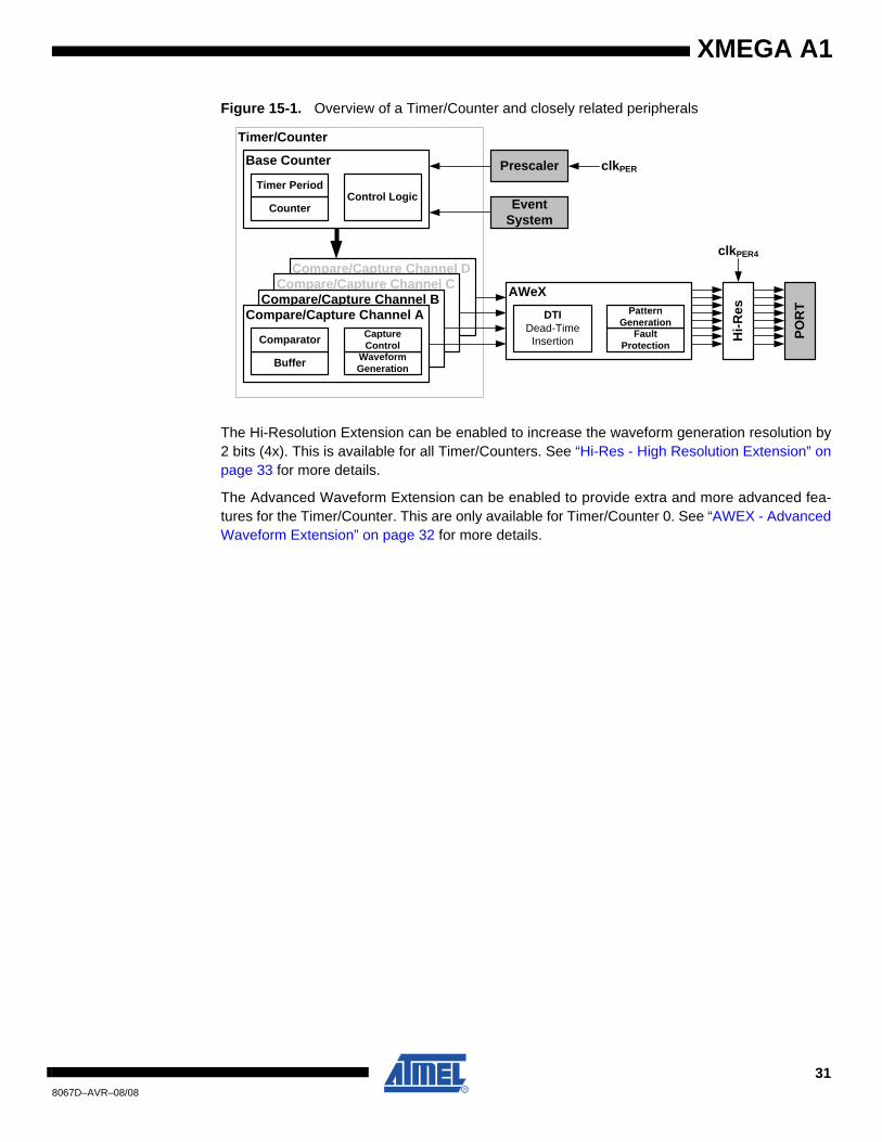
Figure 15-1. Overview of a Timer/Counter and closely related peripherals
The Hi-Resolution Extension can be enabled to increase the waveform generation resolution by2 bits (4x). This is available for all Timer/Counters. See “Hi-Res - High Resolution Extension” onpage 33 for more details.
The Advanced Waveform Extension can be enabled to provide extra and more advanced fea-tures for the Timer/Counter. This are only available for Timer/Counter 0. See “AWEX - AdvancedWaveform Extension” on page 32 for more details.
AWeX
Compare/Capture Channel DCompare/Capture Channel C
Compare/Capture Channel BCompare/Capture Channel A
Waveform GenerationBuffer
Comparator Hi-R
es
Fault Protection
Capture Control
Base Counter
CounterControl Logic
Timer PeriodPrescaler
DTIDead-Time
Insertion
Pattern Generation
clkPER4
POR
T
Event System
clkPER
Timer/Counter
318067D–AVR–08/08
XMEGA A1
16. AWEX - Advanced Waveform Extension
16.1 Features
• Output with complementary output from each Capture channel• Four Dead Time Insertion (DTI) Units, one for each Capture channel• 8-bit DTI Resolution• Separate High and Low Side Dead-Time Setting• Double Buffered Dead-Time• Event Controlled Fault Protection• Single Channel Multiple Output Operation (for BLDC motor control)• Double Buffered Pattern Generation
16.2 Overview
The Advanced Waveform Extension (AWEX) provides extra features to the Timer/Counter inWaveform Generation (WG) modes. The AWEX enables easy and safe implementation of forexample, advanced motor control (AC, BLDC, SR, and Stepper) and power control applications.
Any WG output from a Timer/Counter 0 is split into a complimentary pair of outputs when anyAWEX feature is enabled. These output pairs go through a Dead-Time Insertion (DTI) unit thatenables generation of the non-inverted Low Side (LS) and inverted High Side (HS) of the WGoutput with dead time insertion between LS and HS switching. The DTI output will override thenormal port value according to the port override setting. Optionally the final output can beinverted by using the invert I/O setting for the port pin.
The Pattern Generation unit can be used to generate a synchronized bit pattern on the port it isconnected to. In addition, the waveform generator output from Compare Channel A can be dis-tributed to, and override all port pins. When the Pattern Generator unit is enabled, the DTI unit isbypassed.
The Fault Protection unit is connected to the Event System. This enables any event to trigger afault condition that will disable the AWEX output. Several event channels can be used to triggerfault on several different conditions.
The AWEX is available for TCC0 and TCE0. The notation of these peripherals are AWEXC andAWEXE.
328067D–AVR–08/08
XMEGA A1
17. Hi-Res - High Resolution Extension
17.1 Features• Increases Waveform Generator resolution by 2-bits (4x)• Supports Frequency, single- and dual-slope PWM operation• Supports the AWEX when this is enabled and used for the same Timer/Counter
17.2 OverviewThe Hi-Resolution (Hi-Res) Extension is able to increase the resolution of the waveform genera-tion output by a factor of 4. When enabled for a Timer/Counter, the Fast Peripheral clock runningat four times the CPU clock speed will be as input to the Timer/Counter.
The High Resolution Extension can also be used when an AWEX is enabled and used with aTimer/Counter.
XMEGA A1 devices have four Hi-Res Extensions that each can be enabled for eachTimer/Counters pair on PORTC, PORTD, PORTE and PORTF. The notation of these peripher-als are HIRESC, HIRESD, HIRESE and HIRESF, respectively.
338067D–AVR–08/08
XMEGA A1
18. RTC - 16-bit Real-Time Counter
18.1 Features
• 16-bit Timer• Flexible Tick resolution ranging from 1 Hz to 32.768 kHz• One Compare register• One Period register• Clear timer on Overflow or Compare Match• Overflow or Compare Match event and interrupt generation
18.2 Overview
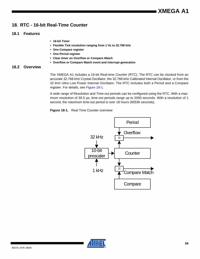
The XMEGA A1 includes a 16-bit Real-time Counter (RTC). The RTC can be clocked from anaccurate 32.768 kHz Crystal Oscillator, the 32.768 kHz Calibrated Internal Oscillator, or from the32 kHz Ultra Low Power Internal Oscillator. The RTC includes both a Period and a Compareregister. For details, see Figure 18-1.
A wide range of Resolution and Time-out periods can be configured using the RTC. With a max-imum resolution of 30.5 µs, time-out periods range up to 2000 seconds. With a resolution of 1second, the maximum time-out period is over 18 hours (65536 seconds).
Figure 18-1. Real Time Counter overview
10-bit prescaler Counter
Period
Compare
=
=
Overflow
Compare Match1 kHz
32 kHz
348067D–AVR–08/08
XMEGA A1
19. TWI - Two-Wire Interface
19.1 Features
• Four Identical TWI peripherals• Simple yet Powerful and Flexible Communication Interface• Both Master and Slave Operation Supported• Device can Operate as Transmitter or Receiver• 7-bit Address Space Allows up to 128 Different Slave Addresses• Multi-master Arbitration Support• Up to 400 kHz Data Transfer Speed• Slew-rate Limited Output Drivers• Noise Suppression Circuitry Rejects Spikes on Bus Lines• Fully Programmable Slave Address with General Call Support• Address Recognition Causes Wake-up when in Sleep Mode• I2C and System Management Bus (SMBus) compatible
19.2 Overview
The Two-Wire Interface (TWI) is a bi-directional wired-AND bus with only two lines, the clock(SCL) line and the data (SDA) line. The protocol makes it possible to interconnect up to 128 indi-vidually addressable devices. Since it is a multi-master bus, one or more devices capable oftaking control of the bus can be connected.
The only external hardware needed to implement the bus is a single pull-up resistor for each ofthe TWI bus lines. Mechanisms for resolving bus contention are inherent in the TWI protocol.
PORTC, PORTD, PORTE, and PORTF each has one TWI. Notation of these peripherals areTWIC, TWID, TWIE, and TWIF, respectively.
358067D–AVR–08/08
XMEGA A1
20. SPI - Serial Peripheral Interface
20.1 Features
• Four Identical SPI peripherals• Full-duplex, Three-wire Synchronous Data Transfer• Master or Slave Operation• LSB First or MSB First Data Transfer• Seven Programmable Bit Rates• End of Transmission Interrupt Flag• Write Collision Flag Protection• Wake-up from Idle Mode• Double Speed (CK/2) Master SPI Mode
20.2 Overview
The Serial Peripheral Interface (SPI) allows high-speed full-duplex, synchronous data transferbetween different devices. Devices can communicate using a master-slave scheme, and data istransferred both to and from the devices simultaneously.
PORTC, PORTD, PORTE, and PORTF each has one SPI. Notation of these peripherals areSPIC, SPID, SPIE, and SPIF, respectively.
368067D–AVR–08/08
XMEGA A1
21. USART
21.1 Features
• Eight Identical USART peripherals• Full Duplex Operation (Independent Serial Receive and Transmit Registers)• Asynchronous or Synchronous Operation• Master or Slave Clocked Synchronous Operation• High-resolution Arithmetic Baud Rate Generator• Supports Serial Frames with 5, 6, 7, 8, or 9 Data Bits and 1 or 2 Stop Bits• Odd or Even Parity Generation and Parity Check Supported by Hardware• Data OverRun Detection• Framing Error Detection• Noise Filtering Includes False Start Bit Detection and Digital Low Pass Filter• Three Separate Interrupts on TX Complete, TX Data Register Empty and RX Complete• Multi-processor Communication Mode• Double Speed Asynchronous Communication Mode• Master SPI mode for SPI communication• IrDA support through the IRCOM module
21.2 Overview
The Universal Synchronous and Asynchronous serial Receiver and Transmitter (USART) is ahighly flexible serial communication module. The USART supports full duplex communication,and both asynchronous and clocked synchronous operation. The USART can also be set inMaster SPI mode to be used for SPI communication.
Communication is frame based, and the frame format can be customized to support a widerange of standards. The USART is buffered in both direction, enabling continued data transmis-sion without any delay between frames. There are separate interrupt vectors for receive andtransmit complete, enabling fully interrupt driven communication. Frame error and buffer over-flow are detected in hardware and indicated with separate status flags. Even or odd paritygeneration and parity check can also be enabled.
One USART can use the IRCOM module to support IrDA 1.4 physical compliant pulse modula-tion and demodulation for baud rates up to 115.2 kbps.
PORTC, PORTD, PORTE, and PORTF each has two USARTs. Notation of these peripheralsare USARTC0, USARTC1, USARTD0, USARTD1, USARTE0, USARTE1, USARTF0,USARTF1, respectively.
378067D–AVR–08/08
XMEGA A1
22. IRCOM - IR Communication Module
22.1 Features
• Pulse modulation/demodulation for infrared communication• Compatible to IrDA 1.4 physical for baud rates up to 115.2 kbps• Selectable pulse modulation scheme
– 3/16 of baud rate period– Fixed pulse period, 8-bit programmable– Pulse modulation disabled
• Built in filtering• Can be connected to and used by one USART at the time
22.2 Overview
XMEGA contains an Infrared Communication Module (IRCOM) for IrDA communication withbaud rates up to 115.2 kbps. This supports three modulation schemes: 3/16 of baud rate period,fixed programmable pulse time based on the Peripheral Clock speed, or pulse modulation dis-abled. There is one IRCOM available which can be connected to any USART to enable infraredpulse coding/decoding for that USART.
388067D–AVR–08/08

XMEGA A1
23. Crypto Engine
23.1 Features
• Data Encryption Standard (DES) CPU instruction• Advanced Encryption Standard (AES) Crypto module• DES Instruction
– Encryption and Decryption– Single-cycle DES instruction– Encryption/Decryption in 16 clock cycles per 8-byte block
• AES Crypto Module– Encryption and Decryption– Support 128-bit keys– Support XOR data load mode to the State memory for Cipher Block Chaining– Encryption/Decryption in 375 clock cycles per 16-byte block
23.2 Overview
The Advanced Encryption Standard (AES) and Data Encryption Standard (DES) are two com-monly used encryption standards. These are supported through an AES peripheral module anda DES CPU instruction. All communication interfaces and the CPU can optionally use AES andDES encrypted communication and data storage.
DES is supported by a DES instruction in the AVR XMEGA CPU. The 8-byte key and 8-bytedata blocks must be loaded into the Register file, and then DES must be executed 16 times toencrypt/decrypt the data block.
The AES Crypto Module encrypts and decrypts 128-bit data blocks with the use of a 128-bit key.The key and data must be loaded into the key and state memory in the module before encryp-tion/decryption is started. It takes 375 peripheral clock cycles before the encryption/decryption isdone and decrypted/encrypted data can be read out, and an optional interrupt can be generated.The AES Crypto Module also has DMA support with transfer triggers when encryption/decryp-tion is done and optional auto-start of encryption/decryption when the state memory is fullyloaded.
398067D–AVR–08/08
XMEGA A1
24. ADC - 12-bit Analog to Digital Converter
24.1 Features
• Two ADCs with 12-bit resolution• 2 Msps sample rate for each ADC• Signed and Unsigned conversions• 4 result registers with individual input channel control for each ADC• 8 single ended inputs for each ADC• 8x4 differential inputs for each ADC• Software selectable gain of 2, 4, 8, 16, 32 or 64• Software selectable resolution of 8- or 12-bit.• Internal or External Reference selection• Event triggered conversion for accurate timing• DMA transfer of conversion results• Interrupt/Event on compare result
24.2 Overview
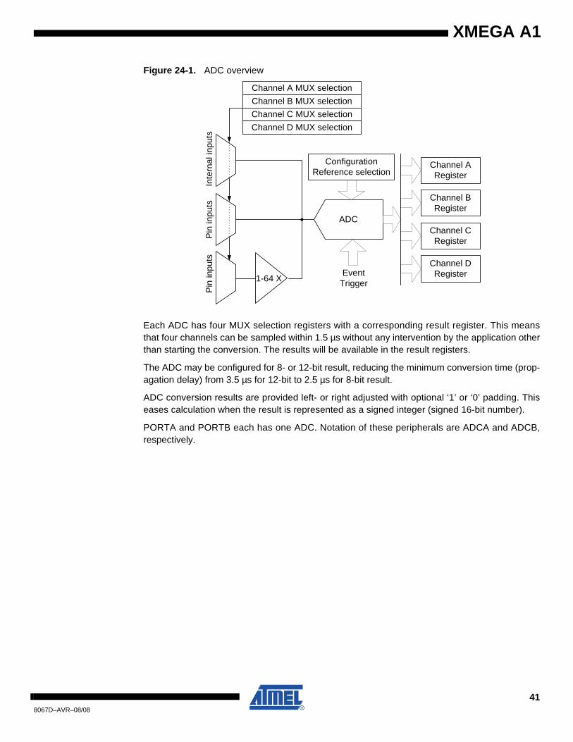
XMEGA A1 devices have two Analog to Digital Converters (ADC), see Figure 24-1 on page 41.The two ADC modules can be operated simultaneously, individually or synchronized.
The ADC converts analog voltages to digital values. The ADC has 12-bit resolution and is capa-ble of converting up to 2 million samples per second. The input selection is flexible, and bothsingle-ended and differential measurements can be performed. The ADC can provide bothsigned and unsigned results, and an optional gain stage is available to increase the dynamicrange of the ADC.
It is a Successive Approximation Result (SAR) ADC. A SAR ADC measures one bit of the con-version result at a time. The ADC has a pipeline architecture. This means that a new analogvoltage can be sampled and a new ADC measurement started on each ADC clock cycle. Eachsample will be converted in the pipeline, where the total sample and conversion time is sevenADC clock cycles for 12-bit result and 5 ADC clock cycles for 8-bit result.
ADC measurements can be started by application software or an incoming event from anotherperipheral in the device. Four different result registers with individual channel selection (MUXregisters) are provided to make it easier for the application to keep track of the data. It is alsopossible to use DMA to move ADC results directly to memory or peripherals.
Both internal and external analog reference voltages can be used. An accurate internal 1.0Vreference is available.
408067D–AVR–08/08
XMEGA A1
Figure 24-1. ADC overview
Each ADC has four MUX selection registers with a corresponding result register. This meansthat four channels can be sampled within 1.5 µs without any intervention by the application otherthan starting the conversion. The results will be available in the result registers.
The ADC may be configured for 8- or 12-bit result, reducing the minimum conversion time (prop-agation delay) from 3.5 µs for 12-bit to 2.5 µs for 8-bit result.
ADC conversion results are provided left- or right adjusted with optional ‘1’ or ‘0’ padding. Thiseases calculation when the result is represented as a signed integer (signed 16-bit number).
PORTA and PORTB each has one ADC. Notation of these peripherals are ADCA and ADCB,respectively.
ADC
Channel A Register
Channel B Register
Channel C Register
Channel D Register
Pin
inpu
tsP
in in
puts
1-64 X
Inte
rnal
inpu
ts
Channel A MUX selectionChannel B MUX selectionChannel C MUX selectionChannel D MUX selection
Event Trigger
ConfigurationReference selection
418067D–AVR–08/08
XMEGA A1
25. DAC - 12-bit Digital to Analog Converter
25.1 Features
• Two DACs with 12-bit resolution• Up to 1 Msps conversion rate for each DAC• Flexible conversion range• Multiple trigger sources• 1 continuous output or 2 Sample and Hold (S/H) outputs for each DAC• Built-in offset and gain calibration• High drive capabilities• Low Power Mode
25.2 Overview
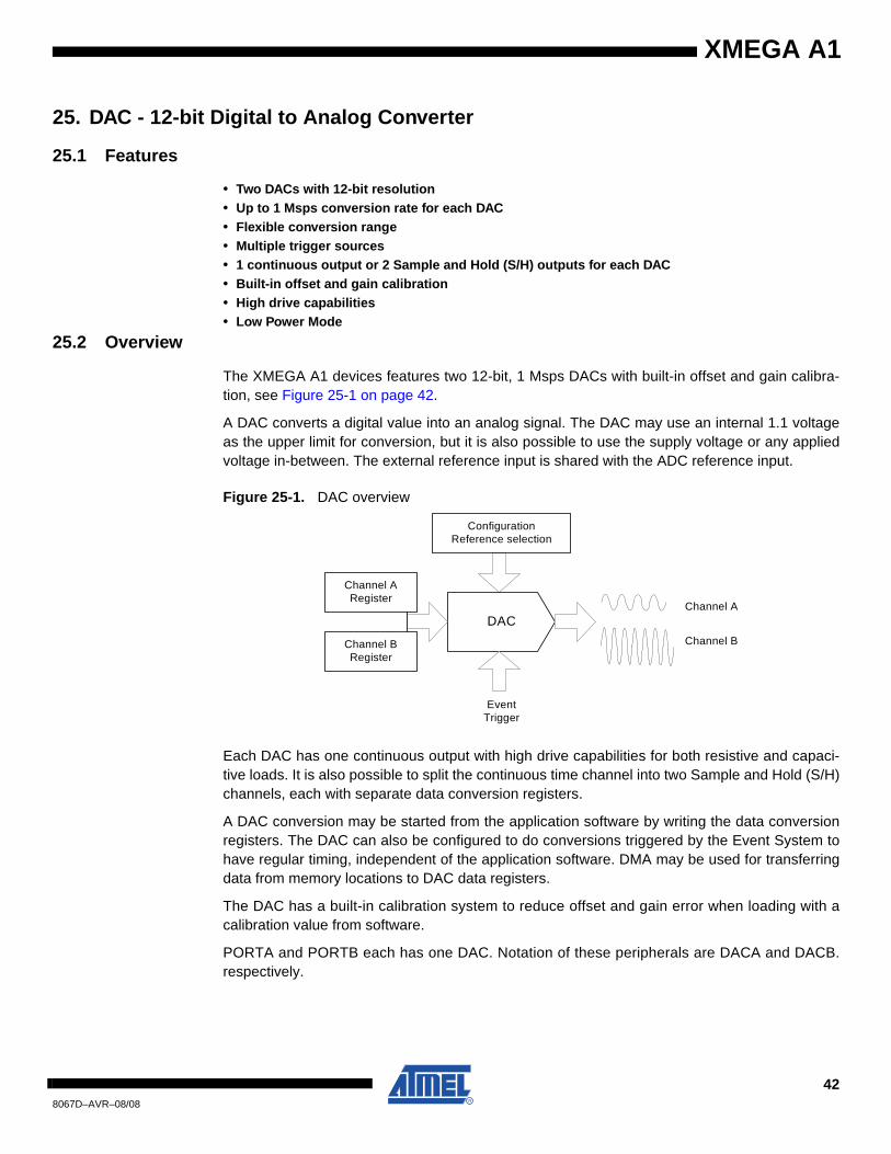
The XMEGA A1 devices features two 12-bit, 1 Msps DACs with built-in offset and gain calibra-tion, see Figure 25-1 on page 42.
A DAC converts a digital value into an analog signal. The DAC may use an internal 1.1 voltageas the upper limit for conversion, but it is also possible to use the supply voltage or any appliedvoltage in-between. The external reference input is shared with the ADC reference input.
Figure 25-1. DAC overview
Each DAC has one continuous output with high drive capabilities for both resistive and capaci-tive loads. It is also possible to split the continuous time channel into two Sample and Hold (S/H)channels, each with separate data conversion registers.
A DAC conversion may be started from the application software by writing the data conversionregisters. The DAC can also be configured to do conversions triggered by the Event System tohave regular timing, independent of the application software. DMA may be used for transferringdata from memory locations to DAC data registers.
The DAC has a built-in calibration system to reduce offset and gain error when loading with acalibration value from software.
PORTA and PORTB each has one DAC. Notation of these peripherals are DACA and DACB.respectively.
DAC
Channel A Register
Channel B Register
Event Trigger
ConfigurationReference selection
Channel A
Channel B
428067D–AVR–08/08
XMEGA A1
26. AC - Analog Comparator
26.1 Features
• Four Analog Comparators• Selectable Power vs. Speed• Selectable hysteresis
– 0, 20 mV, 50 mV• Analog Comparator output available on pin• Flexible Input Selection
– All pins on the port– Output from the DAC– Bandgap reference voltage.– Voltage scaler that can perform a 64-level scaling of the internal VCC voltage.
• Interrupt and event generation on– Rising edge– Falling edge– Toggle
• Window function interrupt and event generation on– Signal above window– Signal inside window– Signal below window
26.2 Overview
XMEGA A1 features four Analog Comparators (AC). An Analog Comparator compares two volt-ages, and the output indicates which input is largest. The Analog Comparator may be configuredto give interrupt requests and/or events upon several different combinations of input change.
Both hysteresis and propagation delays may be adjusted in order to find the optimal operationfor each application.
A wide range of input selection is available, both external pins and several internal signals canbe used.
The Analog Comparators are always grouped in pairs (AC0 and AC1) on each analog port. Theyhave identical behavior but separate control registers.
Optionally, the state of the comparator is directly available on a pin.
PORTA and PORTB each has one AC pair. Notations are ACA and ACB, respectively.
438067D–AVR–08/08
XMEGA A1
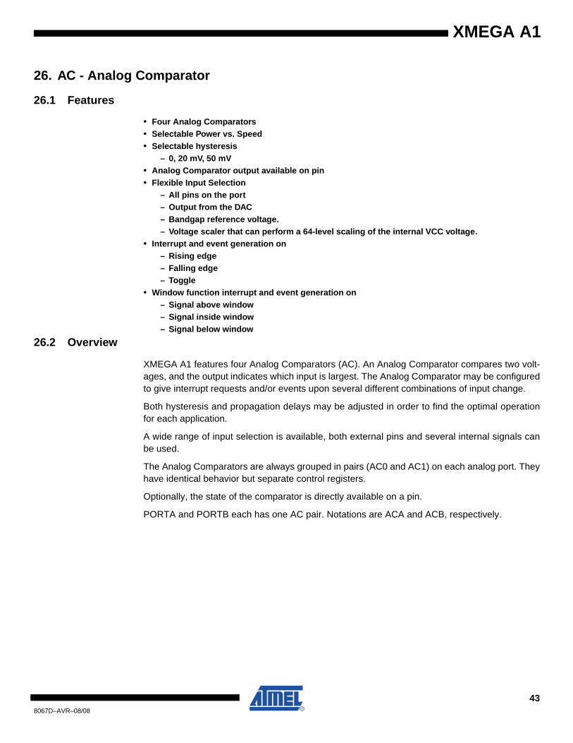
Figure 26-1. Analog comparator overview
AC0
+
-
Pin inputs
Internal inputs
Pin inputs
Internal inputs
VCC scaledInterrupt
sensitivity control
Interrupts
AC1+
-
Pin inputs
Internal inputs
Pin inputs
Internal inputs
VCC scaled
Events
Pin 0 output
448067D–AVR–08/08
XMEGA A1
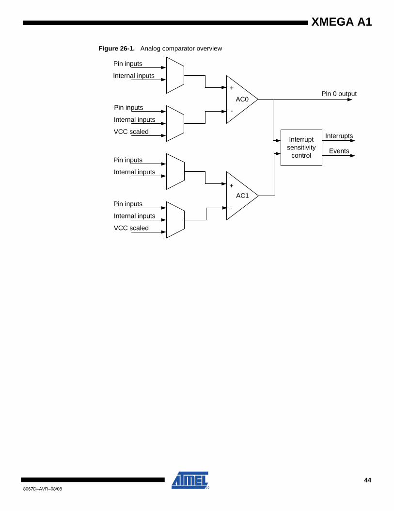
26.3 Input Selection
The Analog comparators have a very flexible input selection and the two comparators groupedin a pair may be used to realize a window function. One pair of analog comparators is shown inFigure 26-1 on page 44.
• Input selection from pin– Pin 0, 1, 2, 3, 4, 5, 6 selectable to positive input of analog comparator– Pin 0, 1, 3, 5, 7 selectable to negative input of analog comparator
• Internal signals available on positive analog comparator inputs– Output from 12-bit DAC
• Internal signals available on negative analog comparator inputs– 64-level scaler of the VCC, available on negative analog comparator input– Bandgap voltage reference– Output from 12-bit DAC
26.4 Window Function
The window function is realized by connecting the external inputs of the two analog comparatorsin a pair as shown in Figure 26-2.
Figure 26-2. Analog comparator window function
AC0
+
-
AC1
+
-
Input signal
Upper limit of window
Lower limit of window
Interrupt sensitivity
control
Interrupts
Events
458067D–AVR–08/08
XMEGA A1
27. OCD - On-chip Debug
27.1 Features
• Complete Program Flow Control– Go, Stop, Reset, Step into, Step over, Step out, Run-to-Cursor
• Debugging on C and high-level language source code level• Debugging on Assembler and disassembler level • 1 dedicated program address or source level breakpoint for AVR Studio / debugger• 4 Hardware Breakpoints• Unlimited Number of User Program Breakpoints• Unlimited Number of User Data Breakpoints, with break on:
– Data location read, write or both read and write– Data location content equal or not equal to a value– Data location content is greater or less than a value– Data location content is within or outside a range– Bits of a data location are equal or not equal to a value
• Non-Intrusive Operation– No hardware or software resources in the device are used
• High Speed Operation– No limitation on debug/programming clock frequency versus system clock frequency
27.2 Overview
The XMEGA A1 has a powerful On-Chip Debug (OCD) system that - in combination with Atmel’sdevelopment tools - provides all the necessary functions to debug an application. It has supportfor program and data breakpoints, and can debug an application from C and high level languagesource code level, as well as assembler and disassembler level. It has full Non-Intrusive Opera-tion and no hardware or software resources in the device are used. The ODC system isaccessed through an external debugging tool which connects to the JTAG or PDI physical inter-faces. Refer to “Program and Debug Interfaces” on page 47.
468067D–AVR–08/08
XMEGA A1
28. Program and Debug Interfaces
28.1 Features
• PDI - Program and Debug Interface (Atmel proprietary 2-pin interface)• JTAG Interface (IEEE std. 1149.1 compliant)• Boundary-scan capabilities according to the IEEE Std. 1149.1 (JTAG)• Access to the OCD system• Programming of Flash, EEPROM, Fuses and Lock Bits
28.2 Overview
The programming and debug facilities are accessed through the JTAG and PDI physical inter-faces. The PDI physical uses one dedicated pin together with the Reset pin, and no generalpurpose pins are used. JTAG uses four general purpose pins on PORTB.
28.3 JTAG interface
The JTAG physical layer handles the basic low-level serial communication over four I/O linesnamed TMS, TCK, TDI, and TDO. It complies to the IEEE Std. 1149.1 for test access port andboundary scan.
28.4 PDI - Program and Debug Interface
The PDI is an Atmel proprietary protocol for communication between the microcontroller andAtmel’s development tools.
478067D–AVR–08/08
XMEGA A1
29. Pinout and Pin Functions
The pinout of XMEGA A1 is shown in “Pinout/Block Diagram” on page 2. In addition to generalI/O functionality, each pin may have several functions. This will depend on which peripheral isenabled and connected to the actual pin. Only one of the alternate pin functions can be used attime.
29.1 Alternate Pin Function Description
The tables below shows the notation for all pin functions available and describes its function.
29.1.1 Operation/Power Supply
29.1.2 Port Interrupt functions
29.1.3 Analog functions
29.1.4 EBI functions
VCC Digital supply voltage
AVCC Analog supply voltage
GND Ground
SYNC Port pin with full synchronous and limited asynchronous interrupt function
ASYNC Port pin with full synchronous and full asynchronous interrupt function
ACn Analog Comparator input pin n
AC0OUT Analog Comparator 0 Output
ADCn Analog to Digital Converter input pin n
DACn Digital to Analog Converter output pin n
AREF Analog Reference input pin
An Address line n
Dn Data line n
CSn Chip Select n
ALEn Address Latch Enable pin n (SRAM)
RE Read Enable (SRAM)
WE External Data Memory Write (SRAM /SDRAM)
BAn Bank Address (SDRAM)
CAS Column Access Strobe (SDRAM)
CKE SDRAM Clock Enable (SDRAM)
CLK SDRAM Clock (SDRAM)
DQM Data Mask Signal/Output Enable (SDRAM)
RAS Row Access Strobe (SDRAM)
488067D–AVR–08/08
XMEGA A1
29.1.5 Timer/Counter and AWEX functions
29.1.6 Communication functions
29.1.7 Oscillators, Clock and Event
29.1.8 Debug/System functions
OCnx Output Compare Channel x for Timer/Counter n
OCxn Inverted Output Compare Channel x for Timer/Counter n
SCL Serial Clock for TWI
SDA Serial Data for TWI
SCLIN Serial Clock In for TWI when external driver interface is enabled
SCLOUT Serial Clock Out for TWI when external driver interface is enabled
SDAIN Serial Data In for TWI when external driver interface is enabled
SDAOUT Serial Data Out for TWI when external driver interface is enabled
XCKn Transfer Clock for USART n
RXDn Receiver Data for USART n
TXDn Transmitter Data for USART n
SS Slave Select for SPI
MOSI Master Out Slave In for SPI
MISO Master In Slave Out for SPI
SCK Serial Clock for SPI
TOSCn Timer Oscillator pin n
XTALn Input/Output for inverting Oscillator pin n
CLKOUT Peripheral Clock Output
EVOUT Event Channel 0 Output
RESET Reset pin
PDI_CLK Program and Debug Interface Clock pin
PDI_DATA Program and Debug Interface Data pin
TCK JTAG Test Clock
TDI JTAG Test Data In
TDO JTAG Test Data Out
TMS JTAG Test Mode Select
498067D–AVR–08/08
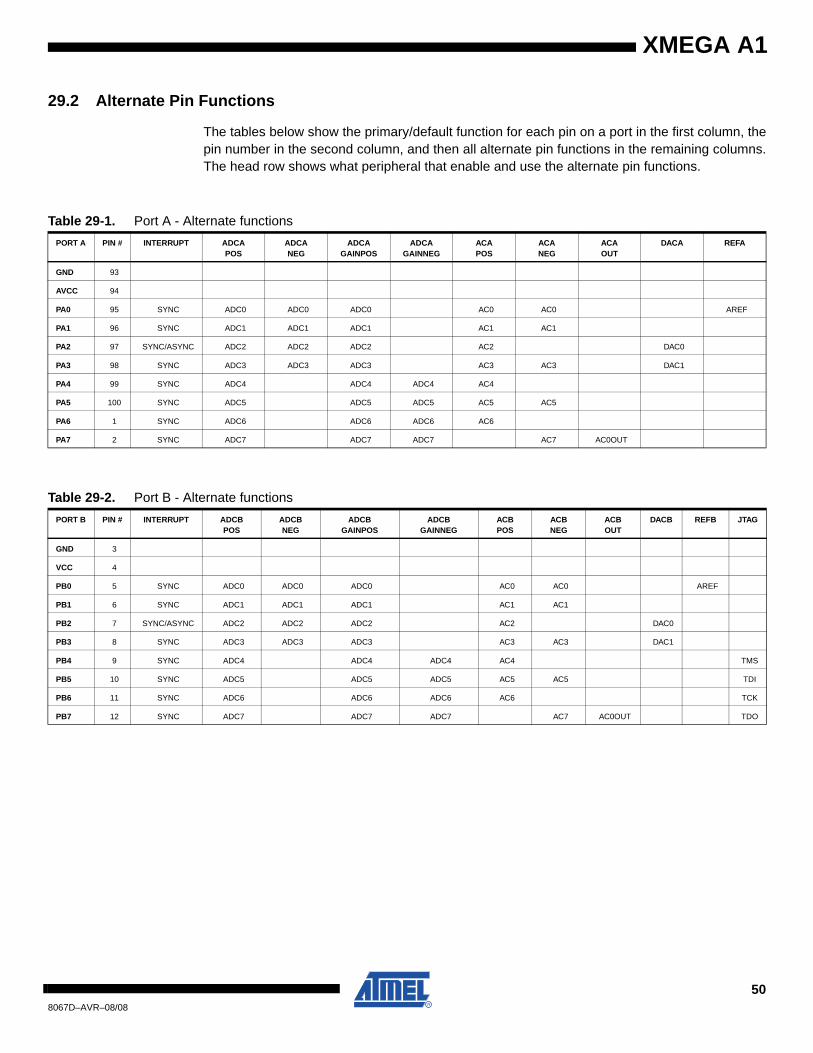
XMEGA A1
29.2 Alternate Pin Functions
The tables below show the primary/default function for each pin on a port in the first column, thepin number in the second column, and then all alternate pin functions in the remaining columns.The head row shows what peripheral that enable and use the alternate pin functions.
Table 29-1. Port A - Alternate functions
PORT A PIN # INTERRUPT ADCAPOS
ADCANEG
ADCAGAINPOS
ADCAGAINNEG
ACAPOS
ACANEG
ACAOUT
DACA REFA
GND 93
AVCC 94
PA0 95 SYNC ADC0 ADC0 ADC0 AC0 AC0 AREF
PA1 96 SYNC ADC1 ADC1 ADC1 AC1 AC1
PA2 97 SYNC/ASYNC ADC2 ADC2 ADC2 AC2 DAC0
PA3 98 SYNC ADC3 ADC3 ADC3 AC3 AC3 DAC1
PA4 99 SYNC ADC4 ADC4 ADC4 AC4
PA5 100 SYNC ADC5 ADC5 ADC5 AC5 AC5
PA6 1 SYNC ADC6 ADC6 ADC6 AC6
PA7 2 SYNC ADC7 ADC7 ADC7 AC7 AC0OUT
Table 29-2. Port B - Alternate functions
PORT B PIN # INTERRUPT ADCBPOS
ADCBNEG
ADCBGAINPOS
ADCBGAINNEG
ACBPOS
ACBNEG
ACBOUT
DACB REFB JTAG
GND 3
VCC 4
PB0 5 SYNC ADC0 ADC0 ADC0 AC0 AC0 AREF
PB1 6 SYNC ADC1 ADC1 ADC1 AC1 AC1
PB2 7 SYNC/ASYNC ADC2 ADC2 ADC2 AC2 DAC0
PB3 8 SYNC ADC3 ADC3 ADC3 AC3 AC3 DAC1
PB4 9 SYNC ADC4 ADC4 ADC4 AC4 TMS
PB5 10 SYNC ADC5 ADC5 ADC5 AC5 AC5 TDI
PB6 11 SYNC ADC6 ADC6 ADC6 AC6 TCK
PB7 12 SYNC ADC7 ADC7 ADC7 AC7 AC0OUT TDO
508067D–AVR–08/08
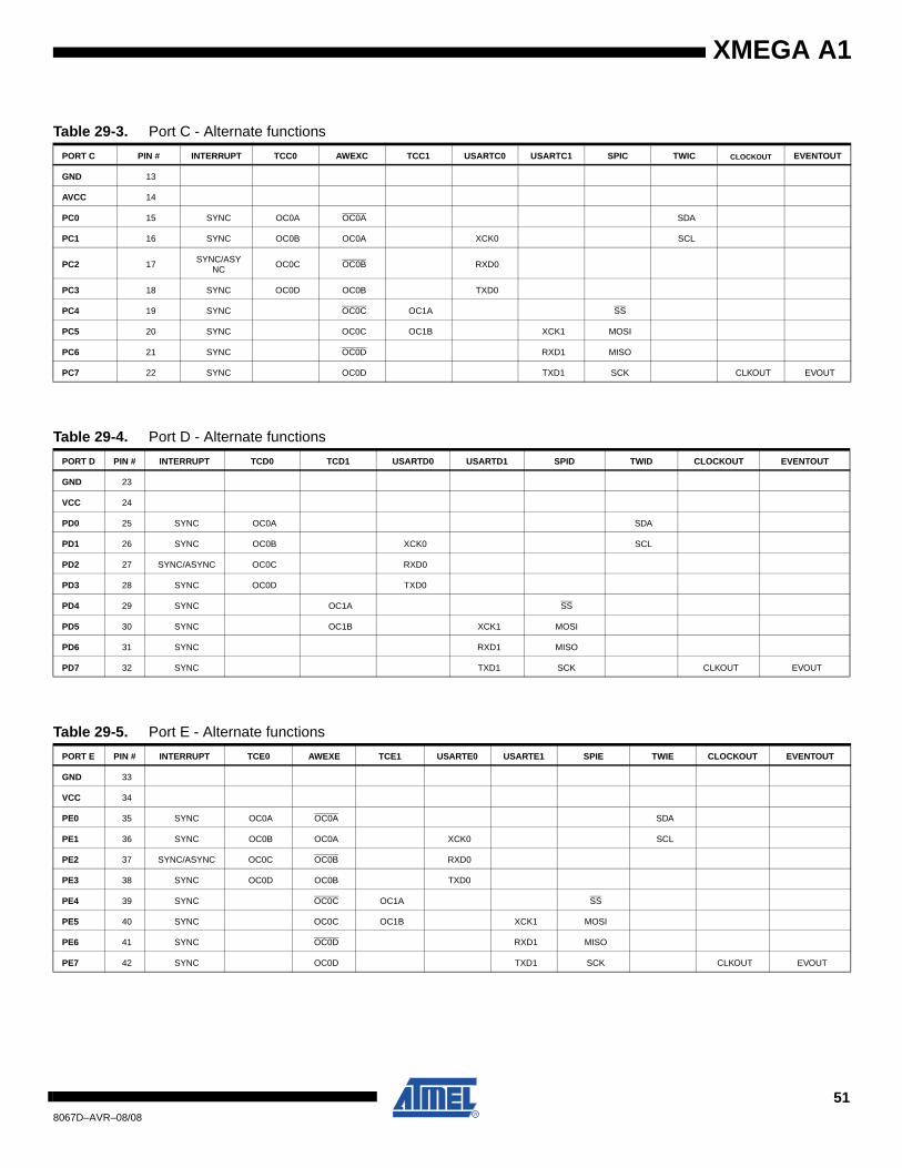
XMEGA A1
Table 29-3. Port C - Alternate functions
PORT C PIN # INTERRUPT TCC0 AWEXC TCC1 USARTC0 USARTC1 SPIC TWIC CLOCKOUT EVENTOUT
GND 13
AVCC 14
PC0 15 SYNC OC0A OC0A SDA
PC1 16 SYNC OC0B OC0A XCK0 SCL
PC2 17SYNC/ASY
NCOC0C OC0B RXD0
PC3 18 SYNC OC0D OC0B TXD0
PC4 19 SYNC OC0C OC1A SS
PC5 20 SYNC OC0C OC1B XCK1 MOSI
PC6 21 SYNC OC0D RXD1 MISO
PC7 22 SYNC OC0D TXD1 SCK CLKOUT EVOUT
Table 29-4. Port D - Alternate functions
PORT D PIN # INTERRUPT TCD0 TCD1 USARTD0 USARTD1 SPID TWID CLOCKOUT EVENTOUT
GND 23
VCC 24
PD0 25 SYNC OC0A SDA
PD1 26 SYNC OC0B XCK0 SCL
PD2 27 SYNC/ASYNC OC0C RXD0
PD3 28 SYNC OC0D TXD0
PD4 29 SYNC OC1A SS
PD5 30 SYNC OC1B XCK1 MOSI
PD6 31 SYNC RXD1 MISO
PD7 32 SYNC TXD1 SCK CLKOUT EVOUT
Table 29-5. Port E - Alternate functions
PORT E PIN # INTERRUPT TCE0 AWEXE TCE1 USARTE0 USARTE1 SPIE TWIE CLOCKOUT EVENTOUT
GND 33
VCC 34
PE0 35 SYNC OC0A OC0A SDA
PE1 36 SYNC OC0B OC0A XCK0 SCL
PE2 37 SYNC/ASYNC OC0C OC0B RXD0
PE3 38 SYNC OC0D OC0B TXD0
PE4 39 SYNC OC0C OC1A SS
PE5 40 SYNC OC0C OC1B XCK1 MOSI
PE6 41 SYNC OC0D RXD1 MISO
PE7 42 SYNC OC0D TXD1 SCK CLKOUT EVOUT
518067D–AVR–08/08
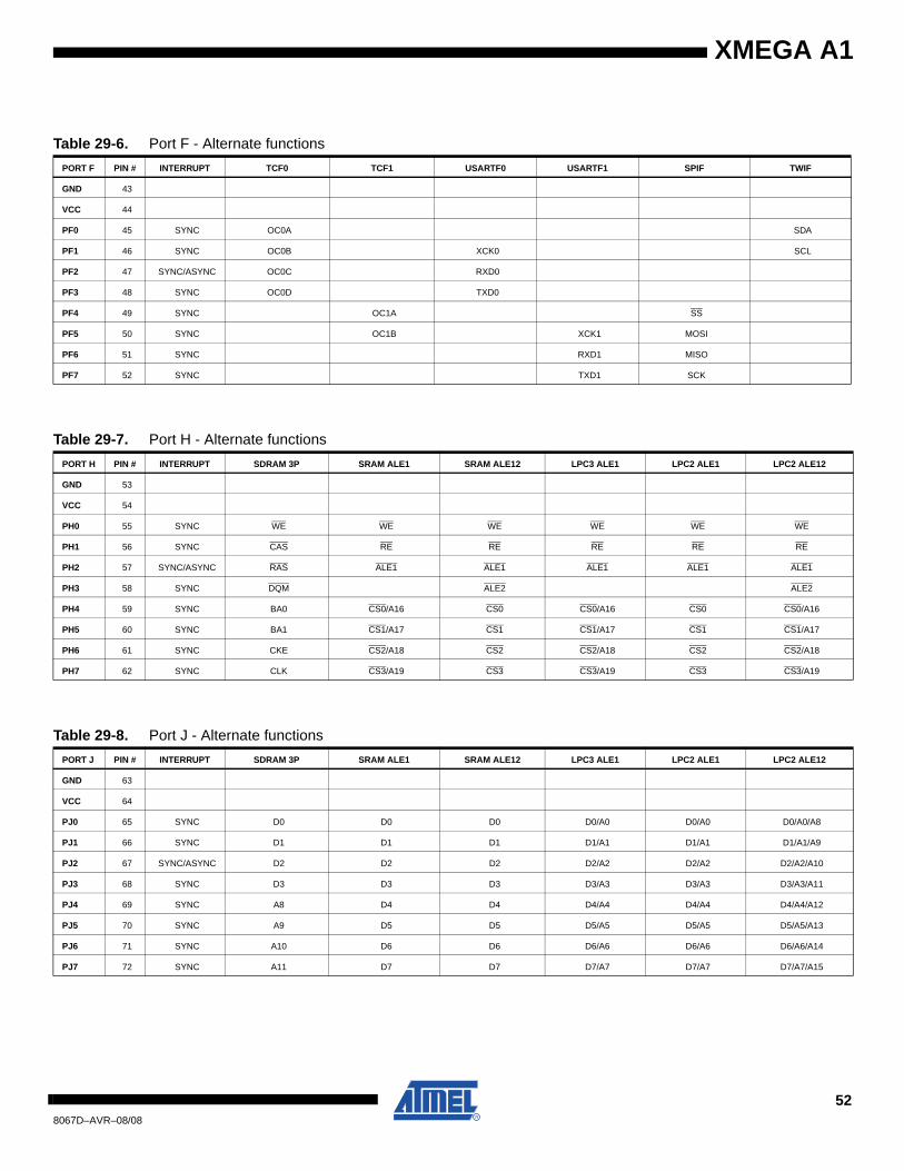
XMEGA A1
Table 29-6. Port F - Alternate functions
PORT F PIN # INTERRUPT TCF0 TCF1 USARTF0 USARTF1 SPIF TWIF
GND 43
VCC 44
PF0 45 SYNC OC0A SDA
PF1 46 SYNC OC0B XCK0 SCL
PF2 47 SYNC/ASYNC OC0C RXD0
PF3 48 SYNC OC0D TXD0
PF4 49 SYNC OC1A SS
PF5 50 SYNC OC1B XCK1 MOSI
PF6 51 SYNC RXD1 MISO
PF7 52 SYNC TXD1 SCK
Table 29-7. Port H - Alternate functions
PORT H PIN # INTERRUPT SDRAM 3P SRAM ALE1 SRAM ALE12 LPC3 ALE1 LPC2 ALE1 LPC2 ALE12
GND 53
VCC 54
PH0 55 SYNC WE WE WE WE WE WE
PH1 56 SYNC CAS RE RE RE RE RE
PH2 57 SYNC/ASYNC RAS ALE1 ALE1 ALE1 ALE1 ALE1
PH3 58 SYNC DQM ALE2 ALE2
PH4 59 SYNC BA0 CS0/A16 CS0 CS0/A16 CS0 CS0/A16
PH5 60 SYNC BA1 CS1/A17 CS1 CS1/A17 CS1 CS1/A17
PH6 61 SYNC CKE CS2/A18 CS2 CS2/A18 CS2 CS2/A18
PH7 62 SYNC CLK CS3/A19 CS3 CS3/A19 CS3 CS3/A19
Table 29-8. Port J - Alternate functions
PORT J PIN # INTERRUPT SDRAM 3P SRAM ALE1 SRAM ALE12 LPC3 ALE1 LPC2 ALE1 LPC2 ALE12
GND 63
VCC 64
PJ0 65 SYNC D0 D0 D0 D0/A0 D0/A0 D0/A0/A8
PJ1 66 SYNC D1 D1 D1 D1/A1 D1/A1 D1/A1/A9
PJ2 67 SYNC/ASYNC D2 D2 D2 D2/A2 D2/A2 D2/A2/A10
PJ3 68 SYNC D3 D3 D3 D3/A3 D3/A3 D3/A3/A11
PJ4 69 SYNC A8 D4 D4 D4/A4 D4/A4 D4/A4/A12
PJ5 70 SYNC A9 D5 D5 D5/A5 D5/A5 D5/A5/A13
PJ6 71 SYNC A10 D6 D6 D6/A6 D6/A6 D6/A6/A14
PJ7 72 SYNC A11 D7 D7 D7/A7 D7/A7 D7/A7/A15
528067D–AVR–08/08
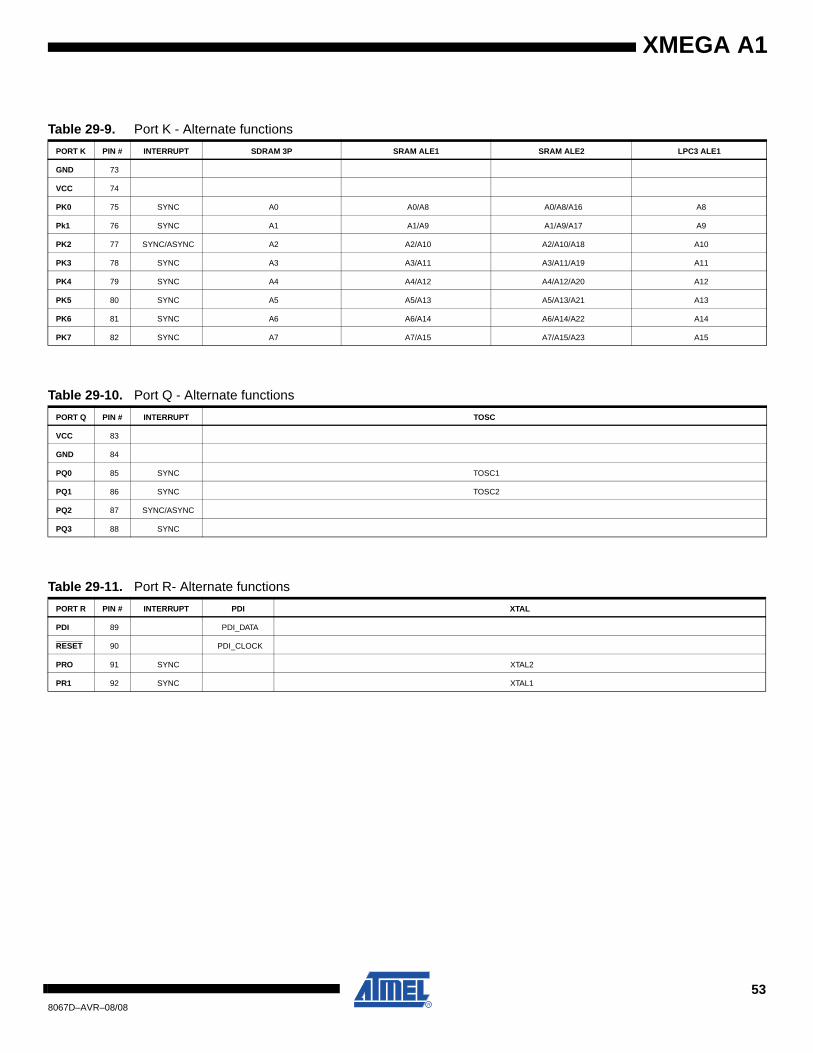
XMEGA A1
Table 29-9. Port K - Alternate functions
PORT K PIN # INTERRUPT SDRAM 3P SRAM ALE1 SRAM ALE2 LPC3 ALE1
GND 73
VCC 74
PK0 75 SYNC A0 A0/A8 A0/A8/A16 A8
Pk1 76 SYNC A1 A1/A9 A1/A9/A17 A9
PK2 77 SYNC/ASYNC A2 A2/A10 A2/A10/A18 A10
PK3 78 SYNC A3 A3/A11 A3/A11/A19 A11
PK4 79 SYNC A4 A4/A12 A4/A12/A20 A12
PK5 80 SYNC A5 A5/A13 A5/A13/A21 A13
PK6 81 SYNC A6 A6/A14 A6/A14/A22 A14
PK7 82 SYNC A7 A7/A15 A7/A15/A23 A15
Table 29-10. Port Q - Alternate functions
PORT Q PIN # INTERRUPT TOSC
VCC 83
GND 84
PQ0 85 SYNC TOSC1
PQ1 86 SYNC TOSC2
PQ2 87 SYNC/ASYNC
PQ3 88 SYNC
Table 29-11. Port R- Alternate functions
PORT R PIN # INTERRUPT PDI XTAL
PDI 89 PDI_DATA
RESET 90 PDI_CLOCK
PRO 91 SYNC XTAL2
PR1 92 SYNC XTAL1
538067D–AVR–08/08
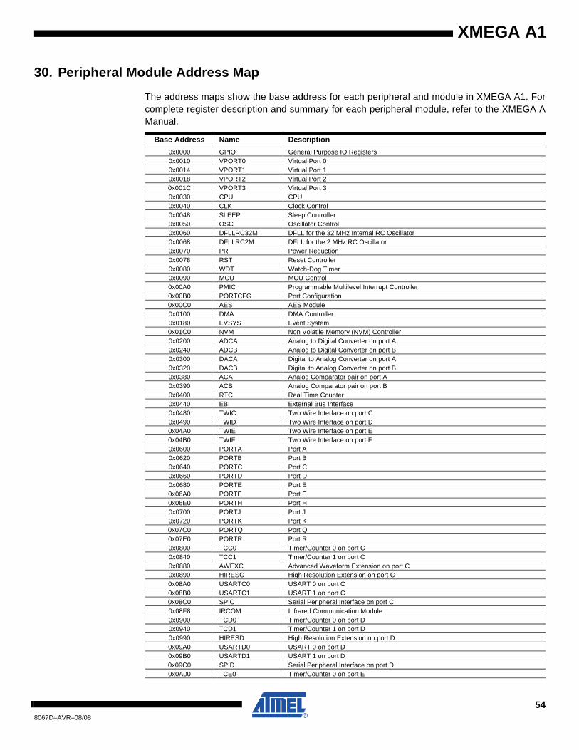
XMEGA A1
30. Peripheral Module Address Map
The address maps show the base address for each peripheral and module in XMEGA A1. Forcomplete register description and summary for each peripheral module, refer to the XMEGA AManual.
Base Address Name Description
0x0000 GPIO General Purpose IO Registers0x0010 VPORT0 Virtual Port 00x0014 VPORT1 Virtual Port 10x0018 VPORT2 Virtual Port 20x001C VPORT3 Virtual Port 30x0030 CPU CPU0x0040 CLK Clock Control0x0048 SLEEP Sleep Controller0x0050 OSC Oscillator Control0x0060 DFLLRC32M DFLL for the 32 MHz Internal RC Oscillator0x0068 DFLLRC2M DFLL for the 2 MHz RC Oscillator0x0070 PR Power Reduction0x0078 RST Reset Controller0x0080 WDT Watch-Dog Timer0x0090 MCU MCU Control0x00A0 PMIC Programmable Multilevel Interrupt Controller0x00B0 PORTCFG Port Configuration0x00C0 AES AES Module0x0100 DMA DMA Controller0x0180 EVSYS Event System0x01C0 NVM Non Volatile Memory (NVM) Controller0x0200 ADCA Analog to Digital Converter on port A0x0240 ADCB Analog to Digital Converter on port B0x0300 DACA Digital to Analog Converter on port A0x0320 DACB Digital to Analog Converter on port B0x0380 ACA Analog Comparator pair on port A0x0390 ACB Analog Comparator pair on port B0x0400 RTC Real Time Counter0x0440 EBI External Bus Interface0x0480 TWIC Two Wire Interface on port C0x0490 TWID Two Wire Interface on port D0x04A0 TWIE Two Wire Interface on port E0x04B0 TWIF Two Wire Interface on port F0x0600 PORTA Port A0x0620 PORTB Port B0x0640 PORTC Port C0x0660 PORTD Port D0x0680 PORTE Port E0x06A0 PORTF Port F0x06E0 PORTH Port H0x0700 PORTJ Port J0x0720 PORTK Port K0x07C0 PORTQ Port Q0x07E0 PORTR Port R0x0800 TCC0 Timer/Counter 0 on port C0x0840 TCC1 Timer/Counter 1 on port C0x0880 AWEXC Advanced Waveform Extension on port C0x0890 HIRESC High Resolution Extension on port C0x08A0 USARTC0 USART 0 on port C0x08B0 USARTC1 USART 1 on port C0x08C0 SPIC Serial Peripheral Interface on port C0x08F8 IRCOM Infrared Communication Module0x0900 TCD0 Timer/Counter 0 on port D0x0940 TCD1 Timer/Counter 1 on port D0x0990 HIRESD High Resolution Extension on port D0x09A0 USARTD0 USART 0 on port D0x09B0 USARTD1 USART 1 on port D0x09C0 SPID Serial Peripheral Interface on port D0x0A00 TCE0 Timer/Counter 0 on port E
548067D–AVR–08/08
XMEGA A1
0x0A40 TCE1 Timer/Counter 1 on port E0x0A80 AWEXE Advanced Waveform Extension on port E0x0A90 HIRESE High Resolution Extension on port E0x0AA0 USARTE0 USART 0 on port E0x0AB0 USARTE1 USART 1 on port E0x0AC0 SPIE Serial Peripheral Interface on port E0x0B00 TCF0 Timer/Counter 0 on port F0x0B40 TCF1 Timer/Counter 1 on port F0x0B90 HIRESF High Resolution Extension on port F0x0BA0 USARTF0 USART 0 on port F0x0BB0 USARTF1 USART 1 on port F0x0BC0 SPIF Serial Peripheral Interface on port F
Base Address Name Description
558067D–AVR–08/08
XMEGA A1
31. Interrupt Vector Summary.
31.1 USART Interrupt vectors
31.2 Timer/Counter Interrupt vectors
Note: 1. Only available on Timer/Counter with 4 Compare or Capture channels 16-bit.
31.3 SPI Interrupt vectors
31.4 TWI Interrupt vectors
Table 31-1. USART Interrupt vectors
Offset Source Interrupt Description
0 RXC USART Receive Complete Interrupt vector offset
2 DRE USART Data Register Empty Interrupt vector offset
4 TXC USART Transmit Complete Interrupt vector offset
Table 31-2. Timer/Counter Interrupt vectors
Offset Source Interrupt Description
0 OVF Timer/Counter Overflow/Underflow Interrupt vector offset
2 ERR Timer/Counter Error Interrupt vector offset
4 CCA Timer/Counter Compare or Capture Channel A Interrupt vector offset
6 CCB Timer/Counter Compare or Capture Channel B Interrupt vector offset
8 CCC(1) Timer/Counter Compare or Capture Channel C Interrupt vector offset
0x0A CCD(1) Timer/Counter Compare or Capture Channel D Interrupt vector offset
Table 31-3. SPI Interrupt vectors
Offset Source Interrupt Description
0 SPI SPI Interrupt vector offset
Table 31-4. TWI Interrupt vectors
Offset Source Interrupt Description
0 MASTER TWI Master Interrupt vector offset
2 SLAVE TWI Slave Interrupt vector offset
568067D–AVR–08/08
XMEGA A1
31.5 DMA Interrupt vectors
31.6 Crystal Oscillator Failure Interrupt vector
31.7 RTC Interrupt vectors
31.8 AES Interrupt vector
31.9 NVM Interrupt vectors
Table 31-5. DMA Interrupt vectors
Offset Source Interrupt Description
0 CH0 DMA Controller Channel 0 Interrupt vector offset
2 CH1 DMA Controller Channel 1 Interrupt vector offset
4 CH2 DMA Controller Channel 2 Interrupt vector offset
6 CH3 DMA Controller Channel 3 Interrupt vector offset
Table 31-6. Crystal Oscillator Failure Interrupt vector
Offset Source Interrupt Description
0 OSCF Crystal Oscillator Failure Interrupt vector (NMI) offset
Table 31-7. RTC Interrupt vectors
Offset Source Interrupt Description
0 COMP Real Time Counter Compare Match Interrupt vector offset
2 PER Real Time Counter Period Interrupt vector offset
Table 31-8. AES Interrupt vector
Offset Source Interrupt Description
0 AES AES Interrupt vector offset
Table 31-9. NVM Interrupt vectors
Offset Source Interrupt Description
0 SPM Non-Volatile Memory SPM Interrupt level vector offset
2 EE Non-Volatile Memory EEPROM Interrupt level vector offset
578067D–AVR–08/08
XMEGA A1
31.10 Analog Comparator Interrupt vectors
31.11 ADC Interrupt vectors
31.12 PORTS Interrupt vectors
Table 31-10. Analog Comparator Interrupt vectors
Offset Source Interrupt Description
0 COMP0 Analog Comparator 0 Interrupt vector offset
2 COMP1 Analog Comparator 1 Interrupt vector offset
4 WINDOW Analog Comparator Window Interrupt vector offset
Table 31-11. Analog to Digital Converter Interrupt vectors
Offset Source Interrupt Description
0 CH0 Analog to Digital Converter Channel 0 Interrupt vector offset
2 CH1 Analog to Digital Converter Channel 1 Interrupt vector offset
4 CH2 Analog to Digital Converter Channel 2 Interrupt vector offset
6 CH3 Analog to Digital Converter Channel 3 Interrupt vector offset
Table 31-12. Ports Interrupt vectors
Offset Source Interrupt Description
0 INT0 Port Interrupt vector 0 offset
2 INT1 Port Interrupt vector 1 offset
588067D–AVR–08/08
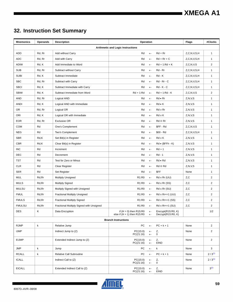
XMEGA A1
32. Instruction Set Summary
Mnemonics Operands Description Operation Flags #Clocks
Arithmetic and Logic Instructions
ADD Rd, Rr Add without Carry Rd ← Rd + Rr Z,C,N,V,S,H 1
ADC Rd, Rr Add with Carry Rd ← Rd + Rr + C Z,C,N,V,S,H 1
ADIW Rd, K Add Immediate to Word Rd ← Rd + 1:Rd + K Z,C,N,V,S 2
SUB Rd, Rr Subtract without Carry Rd ← Rd - Rr Z,C,N,V,S,H 1
SUBI Rd, K Subtract Immediate Rd ← Rd - K Z,C,N,V,S,H 1
SBC Rd, Rr Subtract with Carry Rd ← Rd - Rr - C Z,C,N,V,S,H 1
SBCI Rd, K Subtract Immediate with Carry Rd ← Rd - K - C Z,C,N,V,S,H 1
SBIW Rd, K Subtract Immediate from Word Rd + 1:Rd ← Rd + 1:Rd - K Z,C,N,V,S 2
AND Rd, Rr Logical AND Rd ← Rd • Rr Z,N,V,S 1
ANDI Rd, K Logical AND with Immediate Rd ← Rd • K Z,N,V,S 1
OR Rd, Rr Logical OR Rd ← Rd v Rr Z,N,V,S 1
ORI Rd, K Logical OR with Immediate Rd ← Rd v K Z,N,V,S 1
EOR Rd, Rr Exclusive OR Rd ← Rd ⊕ Rr Z,N,V,S 1
COM Rd One’s Complement Rd ← $FF - Rd Z,C,N,V,S 1
NEG Rd Two’s Complement Rd ← $00 - Rd Z,C,N,V,S,H 1
SBR Rd,K Set Bit(s) in Register Rd ← Rd v K Z,N,V,S 1
CBR Rd,K Clear Bit(s) in Register Rd ← Rd • ($FFh - K) Z,N,V,S 1
INC Rd Increment Rd ← Rd + 1 Z,N,V,S 1
DEC Rd Decrement Rd ← Rd - 1 Z,N,V,S 1
TST Rd Test for Zero or Minus Rd ← Rd • Rd Z,N,V,S 1
CLR Rd Clear Register Rd ← Rd ⊕ Rd Z,N,V,S 1
SER Rd Set Register Rd ← $FF None 1
MUL Rd,Rr Multiply Unsigned R1:R0 ← Rd x Rr (UU) Z,C 2
MULS Rd,Rr Multiply Signed R1:R0 ← Rd x Rr (SS) Z,C 2
MULSU Rd,Rr Multiply Signed with Unsigned R1:R0 ← Rd x Rr (SU) Z,C 2
FMUL Rd,Rr Fractional Multiply Unsigned R1:R0 ← Rd x Rr<<1 (UU) Z,C 2
FMULS Rd,Rr Fractional Multiply Signed R1:R0 ← Rd x Rr<<1 (SS) Z,C 2
FMULSU Rd,Rr Fractional Multiply Signed with Unsigned R1:R0 ← Rd x Rr<<1 (SU) Z,C 2
DES K Data Encryption if (H = 0) then R15:R0else if (H = 1) then R15:R0
←←
Encrypt(R15:R0, K)Decrypt(R15:R0, K)
1/2
Branch Instructions
RJMP k Relative Jump PC ← PC + k + 1 None 2
IJMP Indirect Jump to (Z) PC(15:0)PC(21:16)
←←
Z,0
None 2
EIJMP Extended Indirect Jump to (Z) PC(15:0)PC(21:16)
←←
Z,EIND
None 2
JMP k Jump PC ← k None 3
RCALL k Relative Call Subroutine PC ← PC + k + 1 None 2 / 3(1)
ICALL Indirect Call to (Z) PC(15:0)PC(21:16)
←←
Z,0
None 2 / 3(1)
EICALL Extended Indirect Call to (Z) PC(15:0)PC(21:16)
←←
Z,EIND
None 3(1)
598067D–AVR–08/08
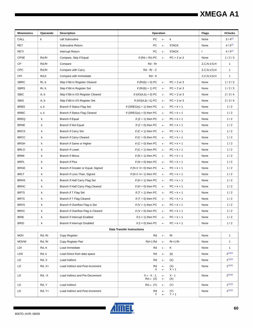
XMEGA A1
CALL k call Subroutine PC ← k None 3 / 4(1)
RET Subroutine Return PC ← STACK None 4 / 5(1)
RETI Interrupt Return PC ← STACK I 4 / 5(1)
CPSE Rd,Rr Compare, Skip if Equal if (Rd = Rr) PC ← PC + 2 or 3 None 1 / 2 / 3
CP Rd,Rr Compare Rd - Rr Z,C,N,V,S,H 1
CPC Rd,Rr Compare with Carry Rd - Rr - C Z,C,N,V,S,H 1
CPI Rd,K Compare with Immediate Rd - K Z,C,N,V,S,H 1
SBRC Rr, b Skip if Bit in Register Cleared if (Rr(b) = 0) PC ← PC + 2 or 3 None 1 / 2 / 3
SBRS Rr, b Skip if Bit in Register Set if (Rr(b) = 1) PC ← PC + 2 or 3 None 1 / 2 / 3
SBIC A, b Skip if Bit in I/O Register Cleared if (I/O(A,b) = 0) PC ← PC + 2 or 3 None 2 / 3 / 4
SBIS A, b Skip if Bit in I/O Register Set If (I/O(A,b) =1) PC ← PC + 2 or 3 None 2 / 3 / 4
BRBS s, k Branch if Status Flag Set if (SREG(s) = 1) then PC ← PC + k + 1 None 1 / 2
BRBC s, k Branch if Status Flag Cleared if (SREG(s) = 0) then PC ← PC + k + 1 None 1 / 2
BREQ k Branch if Equal if (Z = 1) then PC ← PC + k + 1 None 1 / 2
BRNE k Branch if Not Equal if (Z = 0) then PC ← PC + k + 1 None 1 / 2
BRCS k Branch if Carry Set if (C = 1) then PC ← PC + k + 1 None 1 / 2
BRCC k Branch if Carry Cleared if (C = 0) then PC ← PC + k + 1 None 1 / 2
BRSH k Branch if Same or Higher if (C = 0) then PC ← PC + k + 1 None 1 / 2
BRLO k Branch if Lower if (C = 1) then PC ← PC + k + 1 None 1 / 2
BRMI k Branch if Minus if (N = 1) then PC ← PC + k + 1 None 1 / 2
BRPL k Branch if Plus if (N = 0) then PC ← PC + k + 1 None 1 / 2
BRGE k Branch if Greater or Equal, Signed if (N ⊕ V= 0) then PC ← PC + k + 1 None 1 / 2
BRLT k Branch if Less Than, Signed if (N ⊕ V= 1) then PC ← PC + k + 1 None 1 / 2
BRHS k Branch if Half Carry Flag Set if (H = 1) then PC ← PC + k + 1 None 1 / 2
BRHC k Branch if Half Carry Flag Cleared if (H = 0) then PC ← PC + k + 1 None 1 / 2
BRTS k Branch if T Flag Set if (T = 1) then PC ← PC + k + 1 None 1 / 2
BRTC k Branch if T Flag Cleared if (T = 0) then PC ← PC + k + 1 None 1 / 2
BRVS k Branch if Overflow Flag is Set if (V = 1) then PC ← PC + k + 1 None 1 / 2
BRVC k Branch if Overflow Flag is Cleared if (V = 0) then PC ← PC + k + 1 None 1 / 2
BRIE k Branch if Interrupt Enabled if (I = 1) then PC ← PC + k + 1 None 1 / 2
BRID k Branch if Interrupt Disabled if (I = 0) then PC ← PC + k + 1 None 1 / 2
Data Transfer Instructions
MOV Rd, Rr Copy Register Rd ← Rr None 1
MOVW Rd, Rr Copy Register Pair Rd+1:Rd ← Rr+1:Rr None 1
LDI Rd, K Load Immediate Rd ← K None 1
LDS Rd, k Load Direct from data space Rd ← (k) None 2(1)(2)
LD Rd, X Load Indirect Rd ← (X) None 1(1)(2)
LD Rd, X+ Load Indirect and Post-Increment RdX
←←
(X)X + 1
None 1(1)(2)
LD Rd, -X Load Indirect and Pre-Decrement X ← X - 1,Rd ← (X)
←←
X - 1(X)
None 2(1)(2)
LD Rd, Y Load Indirect Rd ← (Y) ← (Y) None 1(1)(2)
LD Rd, Y+ Load Indirect and Post-Increment RdY
←←
(Y)Y + 1
None 1(1)(2)
Mnemonics Operands Description Operation Flags #Clocks
608067D–AVR–08/08
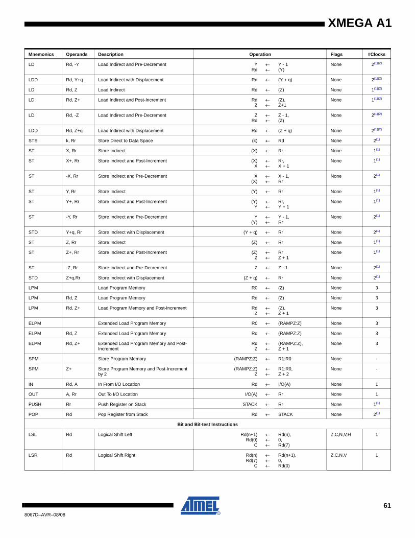
XMEGA A1
LD Rd, -Y Load Indirect and Pre-Decrement YRd
←←
Y - 1(Y)
None 2(1)(2)
LDD Rd, Y+q Load Indirect with Displacement Rd ← (Y + q) None 2(1)(2)
LD Rd, Z Load Indirect Rd ← (Z) None 1(1)(2)
LD Rd, Z+ Load Indirect and Post-Increment RdZ
←←
(Z),Z+1
None 1(1)(2)
LD Rd, -Z Load Indirect and Pre-Decrement ZRd
←←
Z - 1,(Z)
None 2(1)(2)
LDD Rd, Z+q Load Indirect with Displacement Rd ← (Z + q) None 2(1)(2)
STS k, Rr Store Direct to Data Space (k) ← Rd None 2(1)
ST X, Rr Store Indirect (X) ← Rr None 1(1)
ST X+, Rr Store Indirect and Post-Increment (X)X
←←
Rr,X + 1
None 1(1)
ST -X, Rr Store Indirect and Pre-Decrement X(X)
←←
X - 1,Rr
None 2(1)
ST Y, Rr Store Indirect (Y) ← Rr None 1(1)
ST Y+, Rr Store Indirect and Post-Increment (Y)Y
←←
Rr,Y + 1
None 1(1)
ST -Y, Rr Store Indirect and Pre-Decrement Y(Y)
←←
Y - 1,Rr
None 2(1)
STD Y+q, Rr Store Indirect with Displacement (Y + q) ← Rr None 2(1)
ST Z, Rr Store Indirect (Z) ← Rr None 1(1)
ST Z+, Rr Store Indirect and Post-Increment (Z)Z
←←
RrZ + 1
None 1(1)
ST -Z, Rr Store Indirect and Pre-Decrement Z ← Z - 1 None 2(1)
STD Z+q,Rr Store Indirect with Displacement (Z + q) ← Rr None 2(1)
LPM Load Program Memory R0 ← (Z) None 3
LPM Rd, Z Load Program Memory Rd ← (Z) None 3
LPM Rd, Z+ Load Program Memory and Post-Increment RdZ
←←
(Z),Z + 1
None 3
ELPM Extended Load Program Memory R0 ← (RAMPZ:Z) None 3
ELPM Rd, Z Extended Load Program Memory Rd ← (RAMPZ:Z) None 3
ELPM Rd, Z+ Extended Load Program Memory and Post-Increment
RdZ
←←
(RAMPZ:Z),Z + 1
None 3
SPM Store Program Memory (RAMPZ:Z) ← R1:R0 None -
SPM Z+ Store Program Memory and Post-Increment by 2
(RAMPZ:Z)Z
←←
R1:R0,Z + 2
None -
IN Rd, A In From I/O Location Rd ← I/O(A) None 1
OUT A, Rr Out To I/O Location I/O(A) ← Rr None 1
PUSH Rr Push Register on Stack STACK ← Rr None 1(1)
POP Rd Pop Register from Stack Rd ← STACK None 2(1)
Bit and Bit-test Instructions
LSL Rd Logical Shift Left Rd(n+1)Rd(0)
C
←←←
Rd(n),0,Rd(7)
Z,C,N,V,H 1
LSR Rd Logical Shift Right Rd(n)Rd(7)
C
←←←
Rd(n+1),0,Rd(0)
Z,C,N,V 1
Mnemonics Operands Description Operation Flags #Clocks
618067D–AVR–08/08
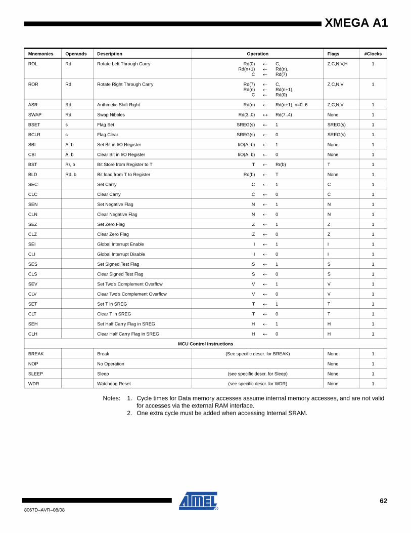
XMEGA A1
Notes: 1. Cycle times for Data memory accesses assume internal memory accesses, and are not valid for accesses via the external RAM interface.
2. One extra cycle must be added when accessing Internal SRAM.
ROL Rd Rotate Left Through Carry Rd(0)Rd(n+1)
C
←←←
C,Rd(n),Rd(7)
Z,C,N,V,H 1
ROR Rd Rotate Right Through Carry Rd(7)Rd(n)
C
←←←
C,Rd(n+1),Rd(0)
Z,C,N,V 1
ASR Rd Arithmetic Shift Right Rd(n) ← Rd(n+1), n=0..6 Z,C,N,V 1
SWAP Rd Swap Nibbles Rd(3..0) ↔ Rd(7..4) None 1
BSET s Flag Set SREG(s) ← 1 SREG(s) 1
BCLR s Flag Clear SREG(s) ← 0 SREG(s) 1
SBI A, b Set Bit in I/O Register I/O(A, b) ← 1 None 1
CBI A, b Clear Bit in I/O Register I/O(A, b) ← 0 None 1
BST Rr, b Bit Store from Register to T T ← Rr(b) T 1
BLD Rd, b Bit load from T to Register Rd(b) ← T None 1
SEC Set Carry C ← 1 C 1
CLC Clear Carry C ← 0 C 1
SEN Set Negative Flag N ← 1 N 1
CLN Clear Negative Flag N ← 0 N 1
SEZ Set Zero Flag Z ← 1 Z 1
CLZ Clear Zero Flag Z ← 0 Z 1
SEI Global Interrupt Enable I ← 1 I 1
CLI Global Interrupt Disable I ← 0 I 1
SES Set Signed Test Flag S ← 1 S 1
CLS Clear Signed Test Flag S ← 0 S 1
SEV Set Two’s Complement Overflow V ← 1 V 1
CLV Clear Two’s Complement Overflow V ← 0 V 1
SET Set T in SREG T ← 1 T 1
CLT Clear T in SREG T ← 0 T 1
SEH Set Half Carry Flag in SREG H ← 1 H 1
CLH Clear Half Carry Flag in SREG H ← 0 H 1
MCU Control Instructions
BREAK Break (See specific descr. for BREAK) None 1
NOP No Operation None 1
SLEEP Sleep (see specific descr. for Sleep) None 1
WDR Watchdog Reset (see specific descr. for WDR) None 1
Mnemonics Operands Description Operation Flags #Clocks
628067D–AVR–08/08
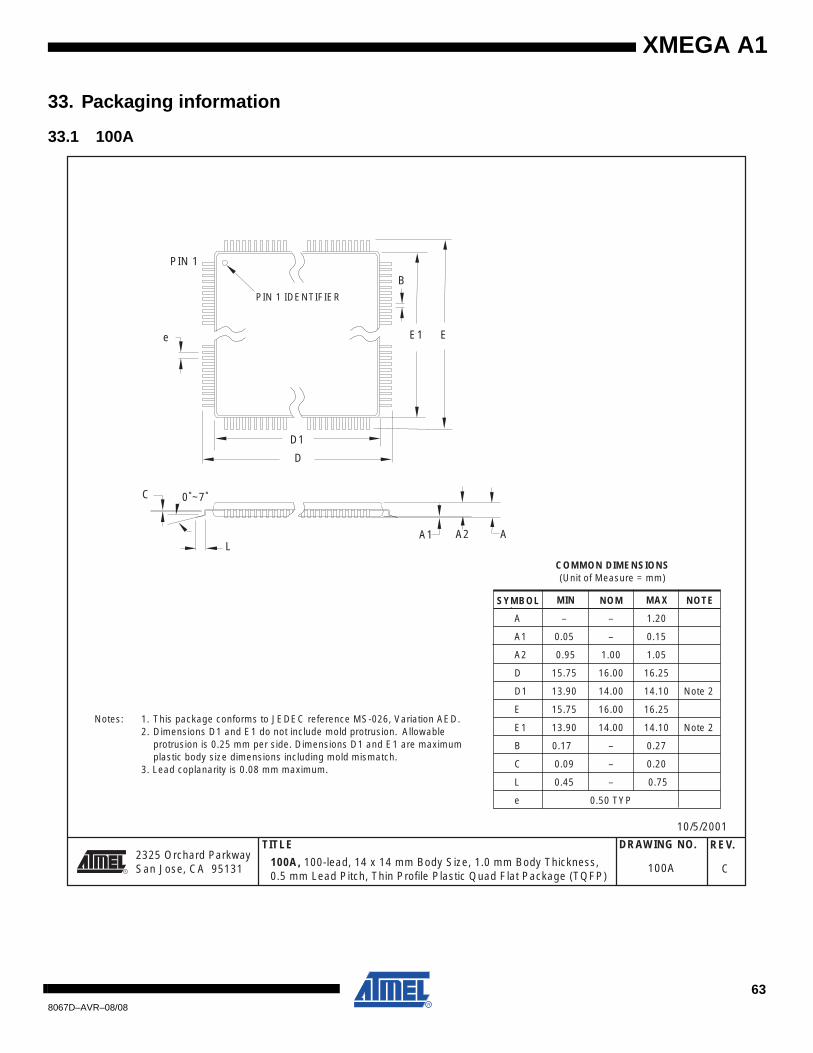
XMEGA A1
33. Packaging information
33.1 100A
2325 Orchard Parkway San Jose, CA 95131
TITLE DRAWING NO.
R
REV.
100A, 100-lead, 14 x 14 mm Body Size, 1.0 mm Body Thickness,0.5 mm Lead Pitch, Thin Profile Plastic Quad Flat Package (TQFP)
C100A
10/5/2001
PIN 1 IDENTIFIER
0˚~7˚
PIN 1
L
C
A1 A2 A
D1
D
e E1 E
B
A – – 1.20
A1 0.05 – 0.15
A2 0.95 1.00 1.05
D 15.75 16.00 16.25
D1 13.90 14.00 14.10 Note 2
E 15.75 16.00 16.25
E1 13.90 14.00 14.10 Note 2
B 0.17 – 0.27
C 0.09 – 0.20
L 0.45 – 0.75
e 0.50 TYP
Notes: 1. This package conforms to JEDEC reference MS-026, Variation AED. 2. Dimensions D1 and E1 do not include mold protrusion. Allowable
protrusion is 0.25 mm per side. Dimensions D1 and E1 are maximum plastic body size dimensions including mold mismatch.
3. Lead coplanarity is 0.08 mm maximum.
COMMON DIMENSIONS(Unit of Measure = mm)
SYMBOL MIN NOM MAX NOTE
638067D–AVR–08/08
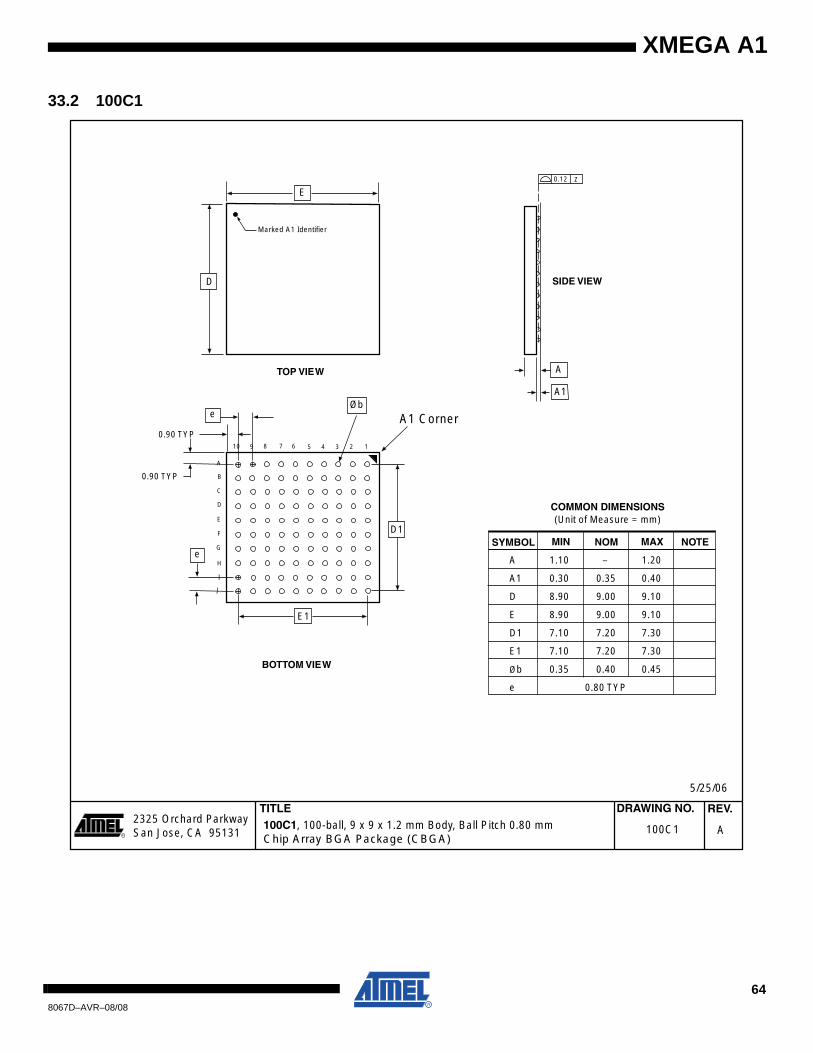
XMEGA A1
33.2 100C1
2325 Orchard Parkway San Jose, CA 95131
TITLE DRAWING NO.
R
REV. 100C1, 100-ball, 9 x 9 x 1.2 mm Body, Ball Pitch 0.80 mm Chip Array BGA Package (CBGA)
A100C1
5/25/06
TOP VIEW
SIDE VIEW
BOTTOM VIEW
COMMON DIMENSIONS(Unit of Measure = mm)
SYMBOL MIN NOM MAX NOTE
A 1.10 – 1.20
A1 0.30 0.35 0.40
D 8.90 9.00 9.10
E 8.90 9.00 9.10
D1 7.10 7.20 7.30
E1 7.10 7.20 7.30
Øb 0.35 0.40 0.45
e 0.80 TYP
Marked A1 Identifier
12345678
A
B
C
D
E
9
F
G
H
I
J
10
0.90 TYP
0.90 TYP
A1 Corner
0.12 Z
E
D
e
e
Øb
A
A1
E1
D1
648067D–AVR–08/08
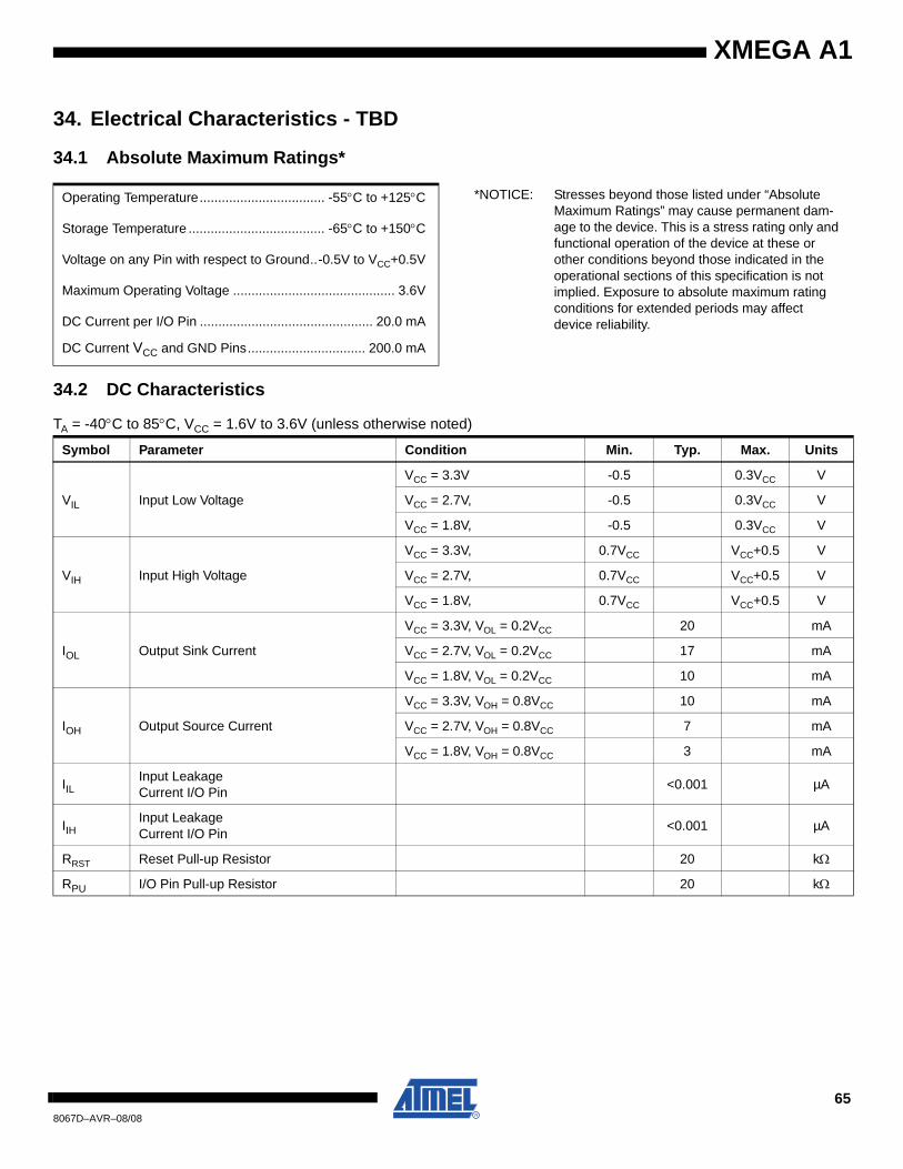
XMEGA A1
34. Electrical Characteristics - TBD
34.1 Absolute Maximum Ratings*
34.2 DC Characteristics
Operating Temperature.................................. -55°C to +125°C *NOTICE: Stresses beyond those listed under “Absolute Maximum Ratings” may cause permanent dam-age to the device. This is a stress rating only and functional operation of the device at these or other conditions beyond those indicated in the operational sections of this specification is not implied. Exposure to absolute maximum rating conditions for extended periods may affect device reliability.
Storage Temperature ..................................... -65°C to +150°C
Voltage on any Pin with respect to Ground..-0.5V to VCC+0.5V
Maximum Operating Voltage ............................................ 3.6V
DC Current per I/O Pin ............................................... 20.0 mA
DC Current VCC and GND Pins................................ 200.0 mA
TA = -40°C to 85°C, VCC = 1.6V to 3.6V (unless otherwise noted)
Symbol Parameter Condition Min. Typ. Max. Units
VIL Input Low Voltage
VCC = 3.3V -0.5 0.3VCC V
VCC = 2.7V, -0.5 0.3VCC V
VCC = 1.8V, -0.5 0.3VCC V
VIH Input High Voltage
VCC = 3.3V, 0.7VCC VCC+0.5 V
VCC = 2.7V, 0.7VCC VCC+0.5 V
VCC = 1.8V, 0.7VCC VCC+0.5 V
IOL Output Sink Current
VCC = 3.3V, VOL = 0.2VCC 20 mA
VCC = 2.7V, VOL = 0.2VCC 17 mA
VCC = 1.8V, VOL = 0.2VCC 10 mA
IOH Output Source Current
VCC = 3.3V, VOH = 0.8VCC 10 mA
VCC = 2.7V, VOH = 0.8VCC 7 mA
VCC = 1.8V, VOH = 0.8VCC 3 mA
IILInput LeakageCurrent I/O Pin
<0.001 µA
IIHInput LeakageCurrent I/O Pin
<0.001 µA
RRST Reset Pull-up Resistor 20 kΩ
RPU I/O Pin Pull-up Resistor 20 kΩ
658067D–AVR–08/08
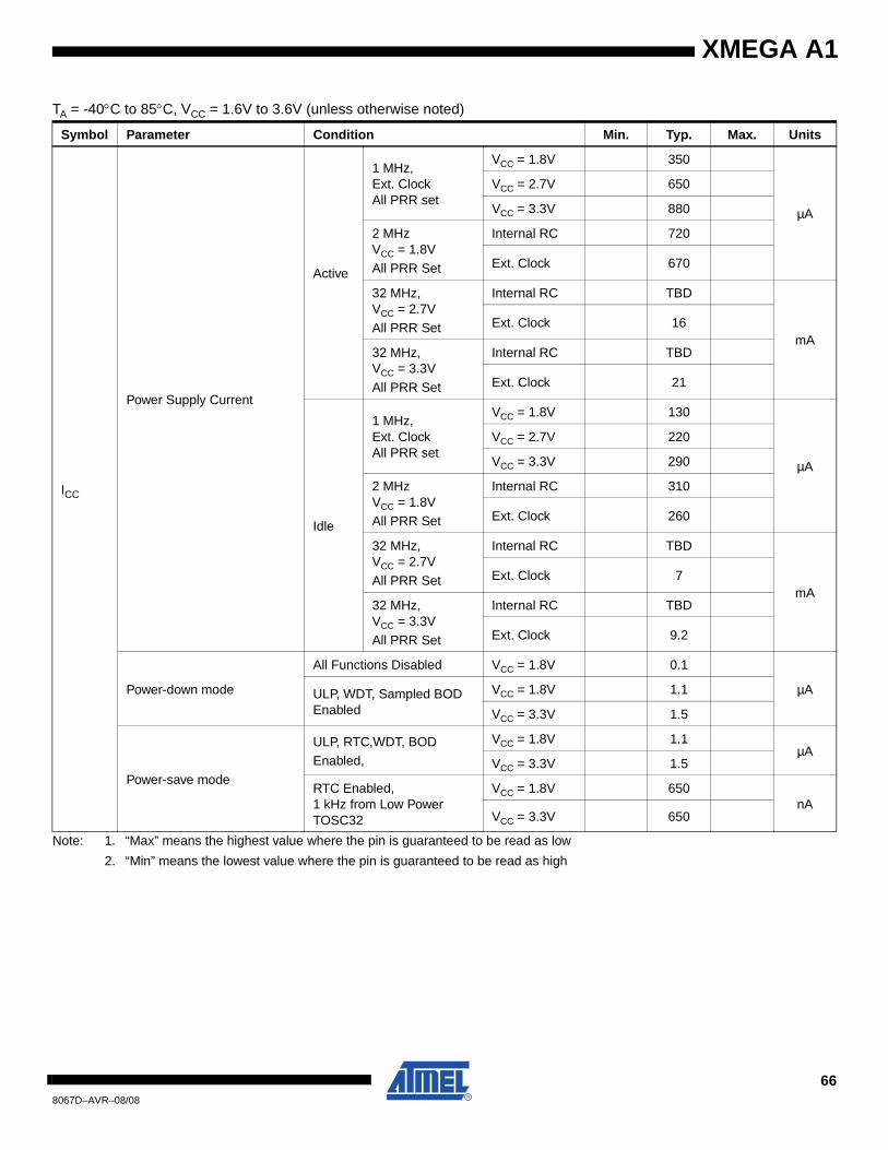
XMEGA A1
Note: 1. “Max” means the highest value where the pin is guaranteed to be read as low
2. “Min” means the lowest value where the pin is guaranteed to be read as high
TA = -40°C to 85°C, VCC = 1.6V to 3.6V (unless otherwise noted)
Symbol Parameter Condition Min. Typ. Max. Units
ICC
Power Supply Current
Active
1 MHz,Ext. ClockAll PRR set
VCC = 1.8V 350
µA
VCC = 2.7V 650
VCC = 3.3V 880
2 MHzVCC = 1.8VAll PRR Set
Internal RC 720
Ext. Clock 670
32 MHz,VCC = 2.7V
All PRR Set
Internal RC TBD
mAExt. Clock 16
32 MHz,VCC = 3.3V
All PRR Set
Internal RC TBD
Ext. Clock 21
Idle
1 MHz,Ext. ClockAll PRR set
VCC = 1.8V 130
µA
VCC = 2.7V 220
VCC = 3.3V 290
2 MHzVCC = 1.8VAll PRR Set
Internal RC 310
Ext. Clock 260
32 MHz,VCC = 2.7V
All PRR Set
Internal RC TBD
mAExt. Clock 7
32 MHz,VCC = 3.3V
All PRR Set
Internal RC TBD
Ext. Clock 9.2
Power-down mode
All Functions Disabled VCC = 1.8V 0.1
µAULP, WDT, Sampled BOD Enabled
VCC = 1.8V 1.1
VCC = 3.3V 1.5
Power-save mode
ULP, RTC,WDT, BODEnabled,
VCC = 1.8V 1.1µA
VCC = 3.3V 1.5
RTC Enabled,1 kHz from Low Power TOSC32
VCC = 1.8V 650nA
VCC = 3.3V 650
668067D–AVR–08/08
XMEGA A1
34.3 Speed
The maximum frequency of the XMEGA A1 devices is depending on VCC. As shown in Figure34-1 on page 67 the Frequency vs. VCC curve is linear between 1.8V < VCC < 2.7V.
Figure 34-1. Maximum Frequency vs. Vcc
1.8
12
32
MHz
V2.7 3.61.6
Safe Operating Area
678067D–AVR–08/08
XMEGA A1
34.4 ADC Characteristics – TBD
Table 34-1. ADC Characteristics
Symbol Parameter Condition Min Typ Max Units
Resolution 8 12 12 LSB
Integral Non-Linearity (INL) TBD LSB
Differential Non-Linearity (DNL) TBD LSB
Gain Error TBD LSB
Offset Error TBD LSB
Conversion Time8-bit Result 2.5 µs
12-bit Result 3.5 µs
ADC Clock Frequency 100 2000 kHz
AVCC DC Supply Voltage 1.6 3.6 V
Source Impedance 2 Msps sample rate 3 kΩ
Start-up time TBD µs
AVCC Analog Supply Voltage VCC - 0.3 VCC + 0.3 V
Table 34-2. ADC Gain Stage Characteristics
Symbol Parameter Condition Min Typ Max Units
Input Capacitance TBD pF
Offset Error
1X Gain,
VCC = 3.3V
AREF = Int. 1.0V -5
LSB
AREF = Ext. 2.5V -3
2X Gain,VCC = 3.3V
AREF = Int. 1.0V -5
AREF = Ext. 2.5V -3
4X Gain,
VCC = 3.3V
AREF = Int. 1.0V -5
AREF = Ext. 2.5V -2.5
8X Gain,
VCC = 3.3V
AREF = Int. 1.0V -5
AREF = Ext. 2.5V -2
16X Gain,VCC = 3.3V
AREF = Int. 1.0V -4
AREF = Ext. 2.5V -1.5
32X Gain,
VCC = 3.3V
AREF = Int. 1.0V -3
AREF = Ext. 2.5V 0
64X Gain,
VCC = 3.3V
AREF = Int. 1.0V 3
AREF = Ext. 2.5V 5
688067D–AVR–08/08
XMEGA A1
Gain Error
1X Gain,
VCC = 3.3V
AREF = Int. 1.0V TBD
LSB
AREF = Ext. 2.5V TBD
2X Gain,
VCC = 3.3V
AREF = Int. 1.0V TBD
AREF = Ext. 2.5V TBD
4X Gain,
VCC = 3.3V
AREF = Int. 1.0V TBD
AREF = Ext. 2.5V TBD
8X Gain,VCC = 3.3V
AREF = Int. 1.0V TBD
AREF = Ext. 2.5V TBD
16X Gain,
VCC = 3.3V
AREF = Int. 1.0V TBD
AREF = Ext. 2.5V TBD
32X Gain,
VCC = 3.3V
AREF = Int. 1.0V TBD
AREF = Ext. 2.5V TBD
64X Gain,VCC = 3.3V
AREF = Int. 1.0V TBD
AREF = Ext. 2.5V TBD
Signal-to-Noise Ratio (SNR)
1X Gain,
VCC = 3.3V
AREF = Int. 1.0V 76.3
dB
AREF = Ext. 1.7V 75.7
AREF = Ext. 2.5V 74.6
2X Gain,
VCC = 3.3V
AREF = Int. 1.0V 71.2
AREF = Ext. 1.7V 72.2
AREF = Ext. 2.5V 71.6
4X Gain,
VCC = 3.3V
AREF = Int. 1.0V 64.8
AREF = Ext. 1.7V 66.8
AREF = Ext. 2.5V 67.7
8X Gain,
VCC = 3.3V
AREF = Int. 1.0V 57.1
AREF = Ext. 1.7V 59.3
AREF = Ext. 2.5V 60.8
16X Gain,
VCC = 3.3V
AREF = Int. 1.0V 48.2
AREF = Ext. 1.7V 50.5
AREF = Ext. 2.5V 52.2
32X Gain,
VCC = 3.3V
AREF = Int. 1.0V 39.3
AREF = Ext. 1.7V 41.6
AREF = Ext. 2.5V 43.2
64X Gain,
VCC = 3.3V
AREF = Int. 1.0V 30.2
AREF = Ext. 1.7V 32.4
AREF = Ext. 2.5V 34.3
Table 34-2. ADC Gain Stage Characteristics (Continued)
Symbol Parameter Condition Min Typ Max Units
698067D–AVR–08/08
XMEGA A1
34.5 DAC Characteristics – TBD
34.6 Analog Comparator Characteristics – TBD
Signal Range TBD V
DC Supply Current TBD mA
Start-up time TBD# clk
cycles
Table 34-2. ADC Gain Stage Characteristics (Continued)
Symbol Parameter Condition Min Typ Max Units
Table 34-3. DAC Characteristics
Symbol Parameter Condition Min Typ Max Units
Resolution 12 12 LSB
Integral Non-Linearity (INL) TBD LSB
Differential Non-Linearity (DNL) TBD LSB
Gain Error TBD LSB
Offset Error TBD LSB
Calibrated Gain/Offset Error TBD LSB
Output Range TBD V
Output Settling Time TBD µs
Output Capacitance TBD nF
Output Resistance TBD kΩ
Reference Input Voltage TBD V
Reference Input Capacitance TBD pF
Reference Input Resistance TBD kΩ
Current Consumption TBD mA
Start-up time TBD µs
Table 34-4. Analog Comparator Characteristics
Symbol Parameter Condition Min Typ Max Units
Offset 0.5 mV
Hysteresis
No, High Speed mode 0
No, Low Power mode 0 mV
Small, High Speed mode 3 mV
Small, Low Power mode 3 mV
Large, High Speed mode 25 mV
Large, Low Power mode 30 mV
Propagation DelayHigh Speed mode 50
nsLow power mode 130
708067D–AVR–08/08
XMEGA A1
Current ConsumptionHigh Speed mode TBD
µALow power mode TBD
Start-up time TBD µs
Table 34-4. Analog Comparator Characteristics
Symbol Parameter Condition Min Typ Max Units
718067D–AVR–08/08
XMEGA A1
35. Typical Characteristics - TBD
728067D–AVR–08/08
XMEGA A1
36. Errata
36.1 ATxmega128A1 rev. G
1. Bootloader Section in Flash is non-functionalThe Bootloader Section is non-functional, and bootloader or application code cannot residein this part of the Flash.
Problem fix/WorkaroundNone, do not use the Bootloader Section.
2. Bandgap voltage input for the ACs cannot be changed when used for both ACssimultaneouslyIf the Bandgap voltage is selected as input for one Analog Comparator (AC) and thenselected/deselected as input for the another AC, the first comparator will be affected for upto 1 us and could potentially give a wrong comparison result.
Problem fix/WorkaroundIf the Bandgap is required for both ACs simultaneously, configure the input selection for bothACs before enabling any of them.
3. DAC is nonlinear and inaccurate when reference is above 2.4VUsing the DAC with a reference voltage above 2.4V give inaccurate output when convertingcodes that give below 0.75V output:
– ±20 LSB for continuous mode
– ±200 LSB for Sample and Hold mode
Problem fix/WorkaroundNone, avoid using a voltage reference above 2.4V.
4. ADC gain stage output range is limited to 2.6 V.The amplified output of the ADC gain stage will never go above 2.6V, hence the differentialinput will only give correct output when below 2.6V/gain. For the available gain settings, thisgives a differential input range of:
– 1X gain: 2.6V
– 2X gain: 1.3V
– 4X gain: 0.65V
– 8X gain: 325 mV
– 16X gain: 163 mV
– 32X gain: 82 mV
– 64X gain: 41 mV
Problem fix/WorkaroundKeep the amplified voltage output from the ADC gain stage below 2.6V in order to get a cor-rect result, or keep ADC voltage reference is below2.6V.
738067D–AVR–08/08
XMEGA A1
5. The ADC has up to ±2 LSB inaccuracyThe ADC will have up to ±2 LSB inaccuracy, visible as a saw-tooth pattern on the input volt-age/ output value transfer function of the ADC. The inaccuracy increases with increasingvoltage reference reaching ±2 LSB with 3V reference.
Problem fix/WorkaroundNone, the actual ADC resolution will be reduced with up to ±2 LSB.
6. TWI, a general address call will match independent of the R/W-bit value.When the TWI is in Slave mode and a general address call is issued on the bus, the TWISlave will get an address match regardless of the R/W-bit (ADDR[0] bit) value in the SlaveAddress Register.
Problem fix/WorkaroundUse software to check the R/W-bit on general call address match.
7. TWI, the minimum I2C SCL low time could be violated in Master Read modeWhen the TWI is in Master Read mode and issuing a Repeated Start on the bus, this willimmediately release the SCL line even if one complete SCL low period has not passed. Thismeans that the minimum SCL low time in the I2C specification could be violated.
Problem fix/WorkaroundIf this causes a potential problem in the application, software must ensure that the RepeatedStart is never issued before one SCL low time has passed.
8. Setting HIRES PR bit makes PWM output unavailableSetting the HIRES Power Reduction (PR) bit for PORTx will make any Frequency or PWMoutput for the corresponding Timer/Counters (TCx0 and TCx1) unavailable on the pin.
Problem fix/WorkaroundDo not write the HIRES PR bit on PORTx when frequency or PWM output from TCx0/1 isused.
9. EEPROM erase and write does not work with all System Clock sourcesWhen doing EEPROM erase or Write operations with other clock sources than the 2 MHzRCOSC, Flash will be read wrongly for one or two clock cycles at the end of the EEPROMoperation.
Problem fix/WorkaroundAlt 1: Use the internal 2 MHz RCOSC when doing erase or write operations on EEPROM.
Alt 2: Ensure to be in sleep mode while completing erase or write on EEPROM. After startingerase or write operations on EEPROM, other interrupts should be disabled and the deviceput to sleep.
748067D–AVR–08/08
XMEGA A1
37. Datasheet Revision History
37.1 8067D – 08/08
37.2 8067C – 06/08
37.3 8067B – 05/08
1. Updated “Ordering Information” on page 2.
2. Updated CBGA pinout in “Pinout/Block Diagram” on page 2
3. Updated “Peripheral Module Address Map” on page 54.
4. Inserted “Interrupt Vector Summary.” on page 56.
1. Updated the Front page and “Features” on page 1.
2. Updated the “DC Characteristics” on page 65.
3. Updated Figure 3-1 on page 5.
4. Added “Flash and EEPROM Page Size” on page 14.
5. Updated Table 34-2 on page 68 with new data: Gain Error, Offset Error and Signal -to-Noise Ratio (SNR).
6. Updated Errata “ATxmega128A1 rev. G” on page 73.
1. Updated “Pinout/Block Diagram” on page 2 and “Pinout and Pin Functions” on page 48.
2. Added XMEGA A1 Block Diagram, Figure 3-1 on page 5.
3. Updated “Overview” on page 4 included the XMEGA A1 explanation text on page 6.
4. Updated AVR CPU “Features” on page 7.
5. Updated Event System block diagram, Figure 9-1 on page 17.
6. Updated “PMIC - Programmable Multi-level Interrupt Controller” on page 24.
7. Updated “AC - Analog Comparator” on page 43.
8. Updated “Alternate Pin Function Description” on page 48.
9. Updated “Alternate Pin Functions” on page 50.
10. Updated “Typical Characteristics - TBD” on page 72.
11. Updated “Ordering Information” on page 2.
12. Updated “Overview” on page 4.
13. Updated Figure 6-1 on page 7.
758067D–AVR–08/08
XMEGA A1
37.4 8067A – 02/08
14. Inserted a new Figure 15-1 on page 31.
15. Updated Speed grades in “Speed” on page 67.
16. Added a new ATxmega384A1 device in “Features” on page 1, updated “Ordering Information” on page 2 and “Memories” on page 9.
17. Replaced the Figure 3-1 on page 5 by a new XMEGA A1 detailed block diagram.
18. Inserted Errata “ATxmega128A1 rev. G” on page 73.
1. Initial revision.
768067D–AVR–08/08
XMEGA A1
Table of Contents
Features ..................................................................................................... 1
Typical Applications ................................................................................ 1
1 Ordering Information ............................................................................... 2
2 Pinout/Block Diagram .............................................................................. 2
3 Overview ................................................................................................... 4
3.1 Block Diagram ...................................................................................................5
4 Resources ................................................................................................. 6
4.1 Recommended reading .....................................................................................6
5 Disclaimer ................................................................................................. 6
6 AVR CPU ................................................................................................... 7
6.1 Features ............................................................................................................7
6.2 Overview ............................................................................................................7
6.3 Register File ......................................................................................................8
6.4 ALU - Arithmetic Logic Unit ...............................................................................8
6.5 Program Flow ....................................................................................................8
7 Memories .................................................................................................. 9
7.1 Features ............................................................................................................9
7.2 Overview ............................................................................................................9
7.3 In-System Programmable Flash Program Memory ...........................................9
7.4 Data Memory ...................................................................................................10
7.5 Calibration Row ...............................................................................................13
7.6 User Signature Row ........................................................................................13
7.7 Flash and EEPROM Page Size .......................................................................14
8 DMAC - Direct Memory Access Controller .......................................... 15
8.1 Features ..........................................................................................................15
8.2 Overview ..........................................................................................................15
9 Event System .......................................................................................... 16
9.1 Features ..........................................................................................................16
9.2 Overview ..........................................................................................................16
10 System Clock and Clock options ......................................................... 18
10.1 Features ..........................................................................................................18
i8067D–AVR–08/08
XMEGA A1
10.2 Overview ..........................................................................................................18
10.3 Clock Options ..................................................................................................19
11 Power Management and Sleep Modes ................................................. 21
11.1 Features ..........................................................................................................21
11.2 Overview ..........................................................................................................21
11.3 Sleep Modes ....................................................................................................21
12 System Control and Reset .................................................................... 22
12.1 Features ..........................................................................................................22
12.2 Resetting the AVR ...........................................................................................22
12.3 Reset Sources .................................................................................................22
12.4 WDT - Watchdog Timer ...................................................................................23
13 PMIC - Programmable Multi-level Interrupt Controller ....................... 24
13.1 Features ..........................................................................................................24
13.2 Overview ..........................................................................................................24
13.3 Interrupt vectors ...............................................................................................24
14 I/O Ports .................................................................................................. 26
14.1 Features ..........................................................................................................26
14.2 Overview ..........................................................................................................26
14.3 I/O configuration ..............................................................................................26
14.4 Input sensing ...................................................................................................29
14.5 Port Interrupt ....................................................................................................29
14.6 Alternate Port Functions ..................................................................................29
15 T/C - 16-bit Timer/Counter ..................................................................... 30
15.1 Features ..........................................................................................................30
15.2 Overview ..........................................................................................................30
16 AWEX - Advanced Waveform Extension ............................................. 32
16.1 Features ..........................................................................................................32
16.2 Overview ..........................................................................................................32
17 Hi-Res - High Resolution Extension ..................................................... 33
17.1 Features ..........................................................................................................33
17.2 Overview ..........................................................................................................33
18 RTC - 16-bit Real-Time Counter ............................................................ 34
18.1 Features ..........................................................................................................34
ii8067D–AVR–08/08
XMEGA A1
18.2 Overview ..........................................................................................................34
19 TWI - Two-Wire Interface ....................................................................... 35
19.1 Features ..........................................................................................................35
19.2 Overview ..........................................................................................................35
20 SPI - Serial Peripheral Interface ............................................................ 36
20.1 Features ..........................................................................................................36
20.2 Overview ..........................................................................................................36
21 USART ..................................................................................................... 37
21.1 Features ..........................................................................................................37
21.2 Overview ..........................................................................................................37
22 IRCOM - IR Communication Module ..................................................... 38
22.1 Features ..........................................................................................................38
22.2 Overview ..........................................................................................................38
23 Crypto Engine ......................................................................................... 39
23.1 Features ..........................................................................................................39
23.2 Overview ..........................................................................................................39
24 ADC - 12-bit Analog to Digital Converter ............................................. 40
24.1 Features ..........................................................................................................40
24.2 Overview ..........................................................................................................40
25 DAC - 12-bit Digital to Analog Converter ............................................. 42
25.1 Features ..........................................................................................................42
25.2 Overview ..........................................................................................................42
26 AC - Analog Comparator ....................................................................... 43
26.1 Features ..........................................................................................................43
26.2 Overview ..........................................................................................................43
26.3 Input Selection .................................................................................................45
26.4 Window Function .............................................................................................45
27 OCD - On-chip Debug ............................................................................ 46
27.1 Features ..........................................................................................................46
27.2 Overview ..........................................................................................................46
28 Program and Debug Interfaces ............................................................. 47
28.1 Features ..........................................................................................................47
28.2 Overview ..........................................................................................................47
iii8067D–AVR–08/08
XMEGA A1
28.3 JTAG interface .................................................................................................47
28.4 PDI - Program and Debug Interface ................................................................47
29 Pinout and Pin Functions ...................................................................... 48
29.1 Alternate Pin Function Description ..................................................................48
29.2 Alternate Pin Functions ...................................................................................50
30 Peripheral Module Address Map .......................................................... 54
31 Interrupt Vector Summary. .................................................................... 56
31.1 USART Interrupt vectors .................................................................................56
31.2 Timer/Counter Interrupt vectors .......................................................................56
31.3 SPI Interrupt vectors ........................................................................................56
31.4 TWI Interrupt vectors .......................................................................................56
31.5 DMA Interrupt vectors ......................................................................................57
31.6 Crystal Oscillator Failure Interrupt vector ........................................................57
31.7 RTC Interrupt vectors ......................................................................................57
31.8 AES Interrupt vector ........................................................................................57
31.9 NVM Interrupt vectors ......................................................................................57
31.10 Analog Comparator Interrupt vectors ..............................................................58
31.11 ADC Interrupt vectors ......................................................................................58
31.12 PORTS Interrupt vectors .................................................................................58
32 Instruction Set Summary ....................................................................... 59
33 Packaging information .......................................................................... 63
33.1 100A ................................................................................................................63
33.2 100C1 ..............................................................................................................64
34 Electrical Characteristics - TBD ............................................................ 65
34.1 Absolute Maximum Ratings* ...........................................................................65
34.2 DC Characteristics ...........................................................................................65
34.3 Speed ..............................................................................................................67
34.4 ADC Characteristics – TBD .............................................................................68
34.5 DAC Characteristics – TBD .............................................................................70
34.6 Analog Comparator Characteristics – TBD .....................................................70
35 Typical Characteristics - TBD ............................................................... 72
36 Errata ....................................................................................................... 73
36.1 ATxmega128A1 rev. G ....................................................................................73
iv8067D–AVR–08/08

37 Datasheet Revision History ................................................................... 75
37.1 8067D – 08/08 .................................................................................................75
37.2 8067C – 06/08 .................................................................................................75
37.3 8067B – 05/08 .................................................................................................75
37.4 8067A – 02/08 .................................................................................................76
Table of Contents....................................................................................... i
Headquarters International
Atmel Corporation2325 Orchard ParkwaySan Jose, CA 95131USATel: 1(408) 441-0311Fax: 1(408) 487-2600
Atmel AsiaRoom 1219Chinachem Golden Plaza77 Mody Road TsimshatsuiEast KowloonHong KongTel: (852) 2721-9778Fax: (852) 2722-1369
Atmel EuropeLe Krebs8, Rue Jean-Pierre TimbaudBP 30978054 Saint-Quentin-en-Yvelines CedexFranceTel: (33) 1-30-60-70-00 Fax: (33) 1-30-60-71-11
Atmel Japan9F, Tonetsu Shinkawa Bldg.1-24-8 ShinkawaChuo-ku, Tokyo 104-0033JapanTel: (81) 3-3523-3551Fax: (81) 3-3523-7581
Product Contact
Web Sitewww.atmel.com
Technical [email protected]
Sales Contactwww.atmel.com/contacts
Literature Requestswww.atmel.com/literature
Disclaimer: The information in this document is provided in connection with Atmel products. No license, express or implied, by estoppel or otherwise, to anyintellectual property right is granted by this document or in connection with the sale of Atmel products. EXCEPT AS SET FORTH IN ATMEL’S TERMS AND CONDI-TIONS OF SALE LOCATED ON ATMEL’S WEB SITE, ATMEL ASSUMES NO LIABILITY WHATSOEVER AND DISCLAIMS ANY EXPRESS, IMPLIED OR STATUTORYWARRANTY RELATING TO ITS PRODUCTS INCLUDING, BUT NOT LIMITED TO, THE IMPLIED WARRANTY OF MERCHANTABILITY, FITNESS FOR A PARTICULARPURPOSE, OR NON-INFRINGEMENT. IN NO EVENT SHALL ATMEL BE LIABLE FOR ANY DIRECT, INDIRECT, CONSEQUENTIAL, PUNITIVE, SPECIAL OR INCIDEN-TAL DAMAGES (INCLUDING, WITHOUT LIMITATION, DAMAGES FOR LOSS OF PROFITS, BUSINESS INTERRUPTION, OR LOSS OF INFORMATION) ARISING OUT OFTHE USE OR INABILITY TO USE THIS DOCUMENT, EVEN IF ATMEL HAS BEEN ADVISED OF THE POSSIBILITY OF SUCH DAMAGES. Atmel makes norepresentations or warranties with respect to the accuracy or completeness of the contents of this document and reserves the right to make changes to specificationsand product descriptions at any time without notice. Atmel does not make any commitment to update the information contained herein. Unless specifically providedotherwise, Atmel products are not suitable for, and shall not be used in, automotive applications. Atmel’s products are not intended, authorized, or warranted for useas components in applications intended to support or sustain life.
© 2008 Atmel Corporation. All rights reserved. Atmel®, logo and combinations thereof, AVR® and others are registered trademarks, XMEGATM
and others are trademarks of Atmel Corporation or its subsidiaries. Other terms and product names may be trademarks of others.
8067D–AVR–08/08