Embed Size (px)
Citation preview
Lecture 16-1
IC implementations• So far, we talked mostly about discrete circuits...
• In IC:
• Very rare use of capacitors, inductors practically never (only in some RF circuits)
• - you typically do not have resistors > several K Ohm,
• - the larger resistance, the more expensive it is,
• - a resistor is much more expensive than a bunch of transistors!
9V
10kΩ
10kΩ
9V
1kΩ
1kΩ
9V
270kΩ
100kΩ
3.3V
Lecture 16-2
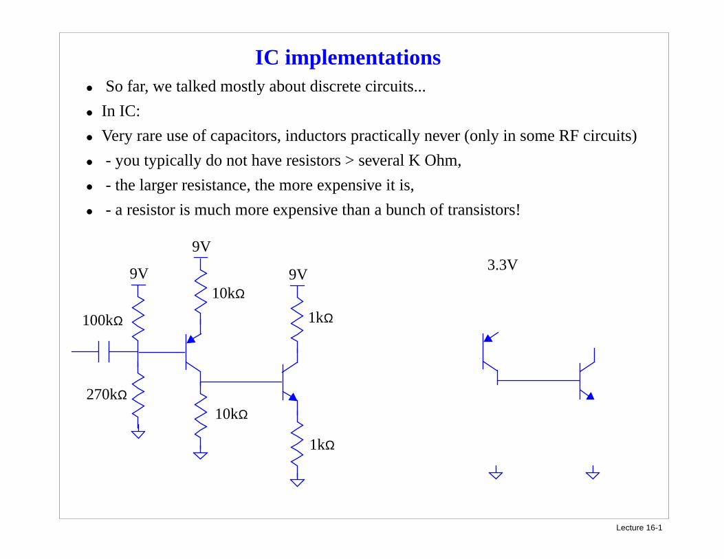
Opamps
• Previously we looked at the block-level internal structure of an operational amplifier
• We are now starting to look at the transistor level implementations of these blocks
• What sort of amplifier circuits would you propose for the blocks below based on what you’ve seen so far?
vo
vid
1
2+
_
+
_
Gm
C (compensation capacitor)
+1µ–
DifferentialInput Trans-conductanceAmplifier
VoltageAmplifier
Unity-GainBuffer
Lecture 16-3
Opamps
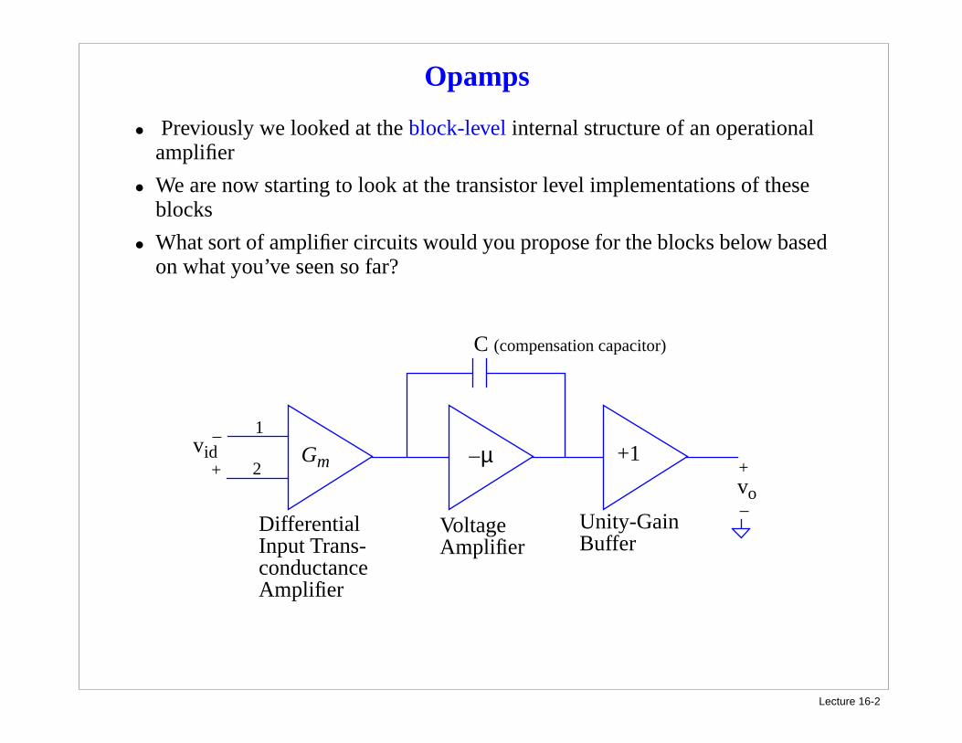
• We macromodeled these blocks in the following way:
vo
1
2
+
_
C
Gmvid Ro1 Ri2
+
_
µvi2–vi2
• What do the R’s represent?
vid+
_
Lecture 16-4
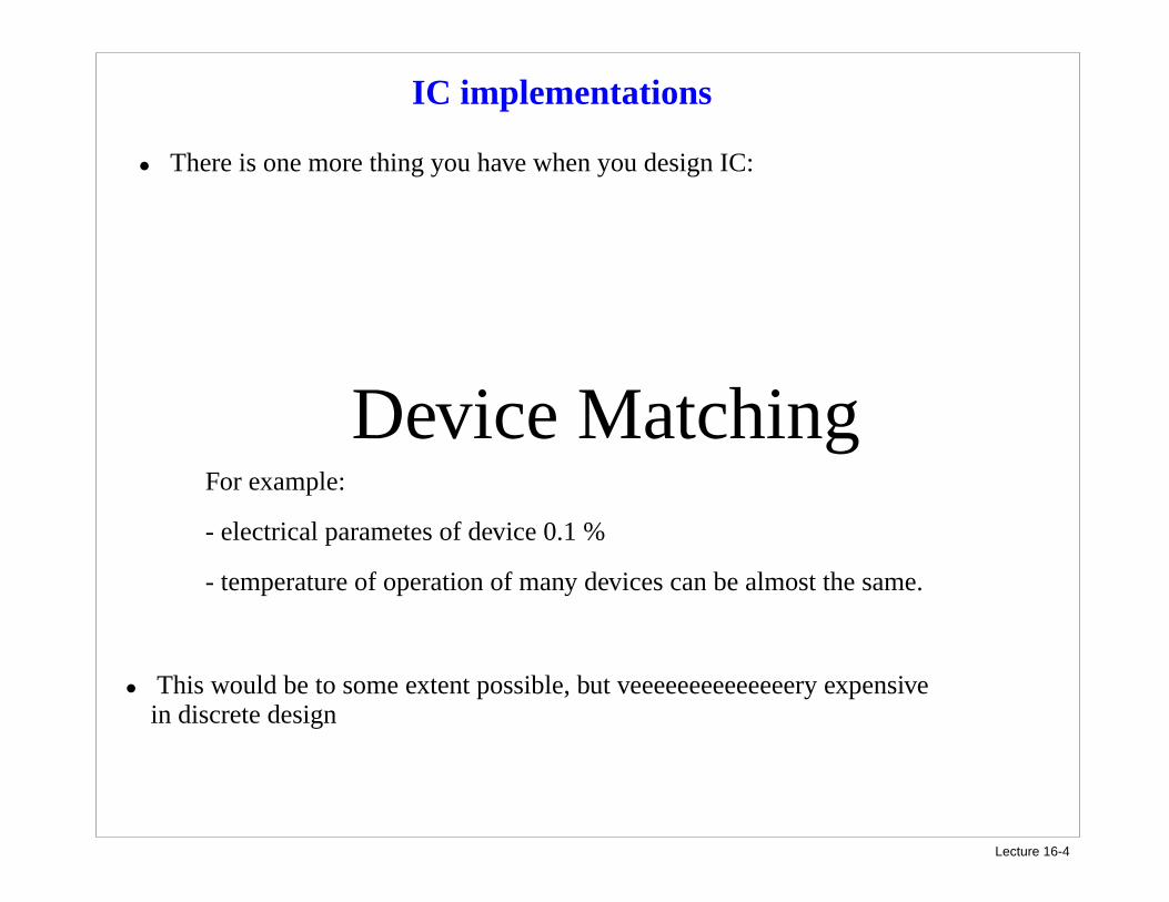
IC implementations
• There is one more thing you have when you design IC:
Device Matching
• This would be to some extent possible, but veeeeeeeeeeeeeery expensive in discrete design
For example:
- electrical parametes of device 0.1 %
- temperature of operation of many devices can be almost the same.
Lecture 16-5
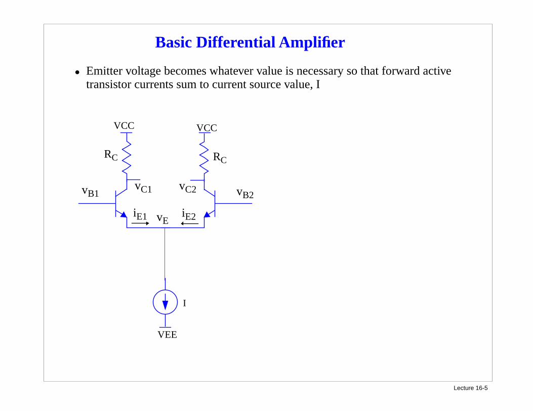
Basic Differential Amplifier
• Emitter voltage becomes whatever value is necessary so that forward active transistor currents sum to current source value, I
VCC
RC
vB1
VCC
RC
vB2 vC1 vC2
I
vE iE1 iE2
VEE
Lecture 16-6
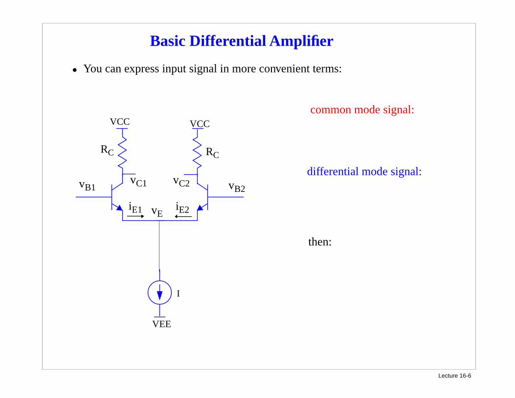
Basic Differential Amplifier
• You can express input signal in more convenient terms:
VCC
RC
vB1
VCC
RC
vB2 vC1 vC2
I
vE iE1 iE2
VEE
common mode signal:
differential mode signal:
then:
Lecture 16-7
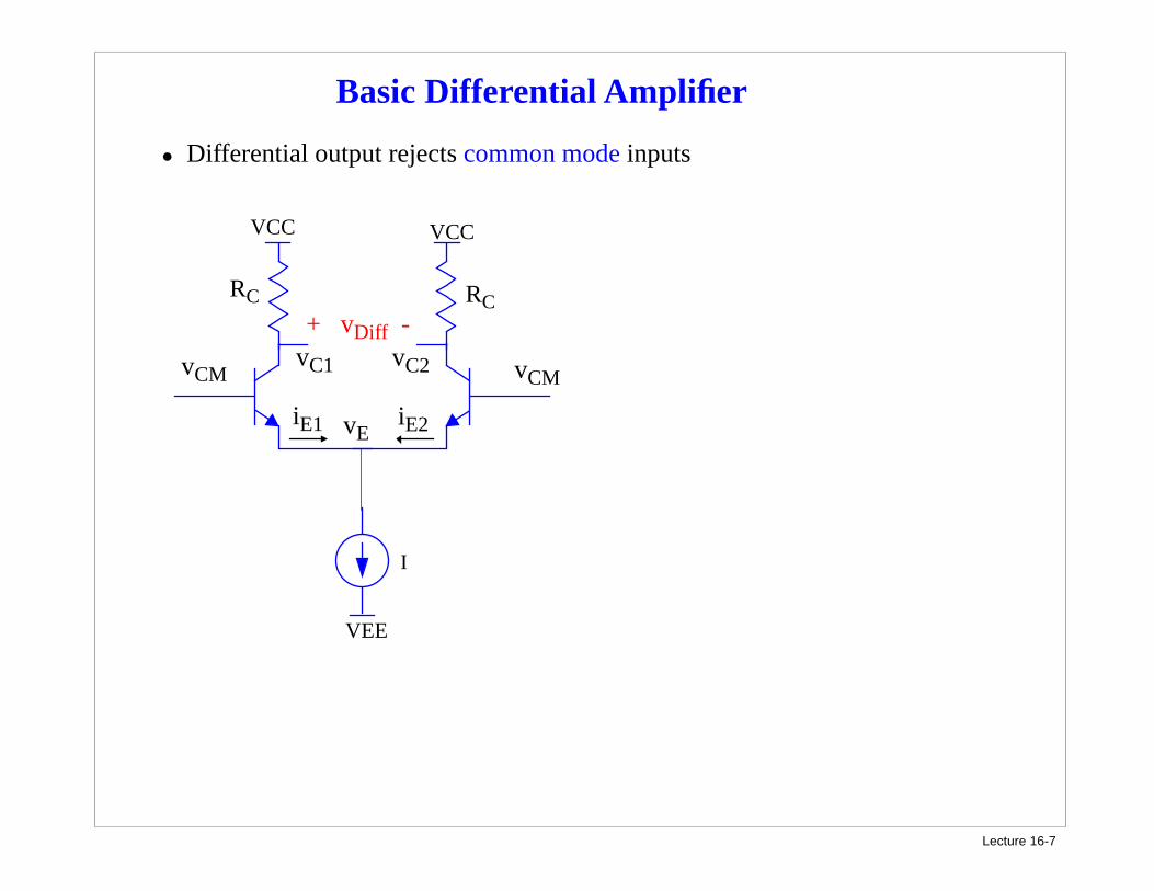
Basic Differential Amplifier
• Differential output rejects common mode inputs
VCC
RC
vCM
VCC
RC
vCMvC1 vC2
I
vE iE1 iE2
VEE
+ vDiff -
Lecture 16-8
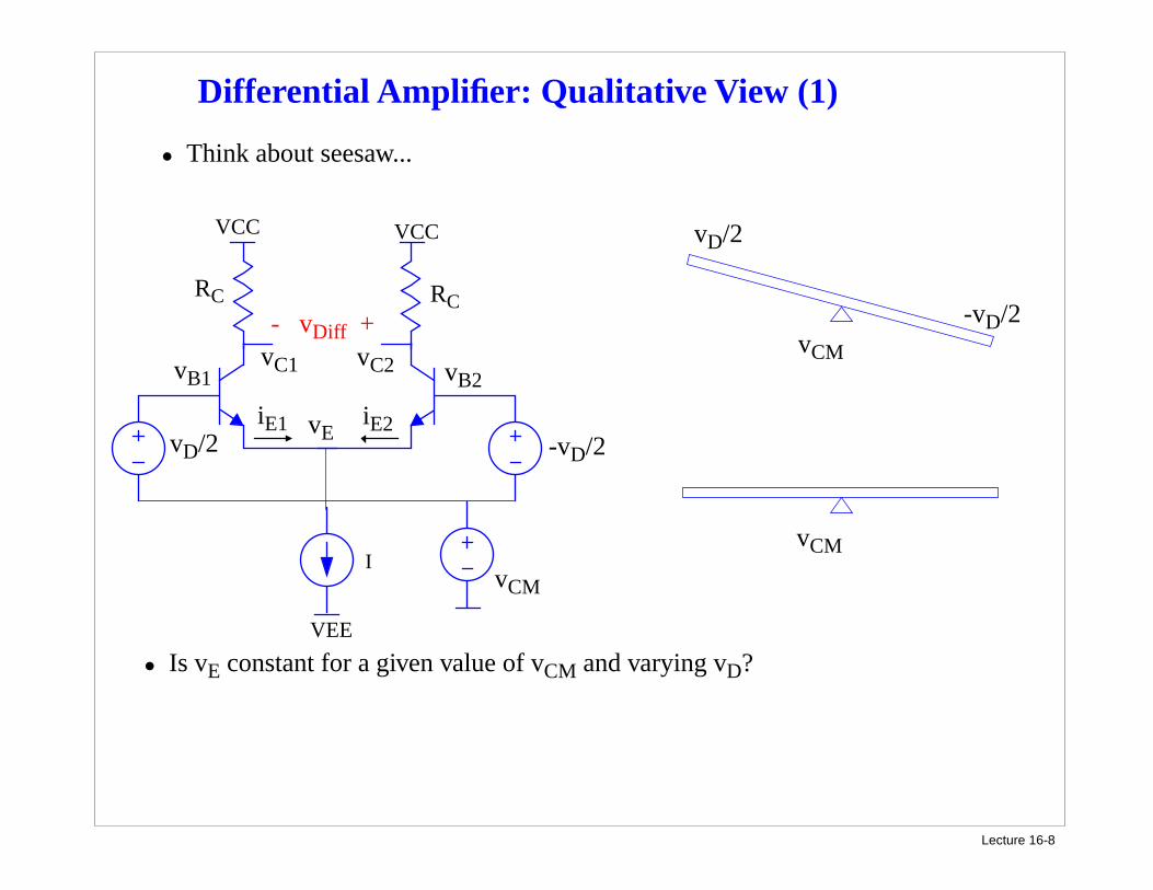
Differential Amplifier: Qualitative View (1)
• Think about seesaw...
VCC
RC
VCC
RC
vCM
vC1 vC2
I
vE iE1 iE2
VEE
- vDiff +
-vD/2 vD/2
vCM
-vD/2
vD/2
vCMvB1 vB2
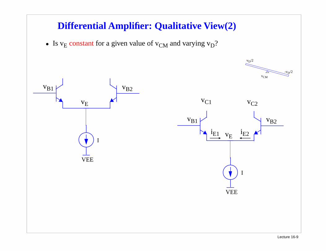
• Is vE constant for a given value of vCM and varying vD?
Lecture 16-9
Differential Amplifier: Qualitative View(2)
• Is vE constant for a given value of vCM and varying vD?
I
vE
VEE
-vD/2
vD/2
vCM
vB1 vB2
vC1 vC2
I
vE iE1 iE2
VEE
vB1 vB2
Lecture 16-10
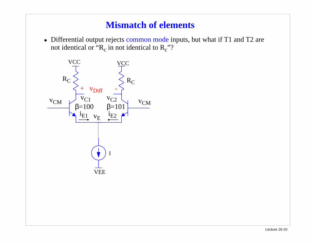
Mismatch of elements• Differential output rejects common mode inputs, but what if T1 and T2 are
not identical or “Rc in not identical to Rc”?
VCC
RC
vCM
VCC
RC
vCM vC1 vC2
I
vE iE1 iE2
VEE
+ vDiff -
β=100 β=101
Lecture 16-11
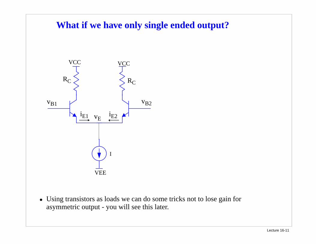
What if we have only single ended output?
• Using transistors as loads we can do some tricks not to lose gain for asymmetric output - you will see this later.
VCC
RC
VCC
RC
vB2
I
vE iE1 iE2
VEE
vB1
Lecture 16-12
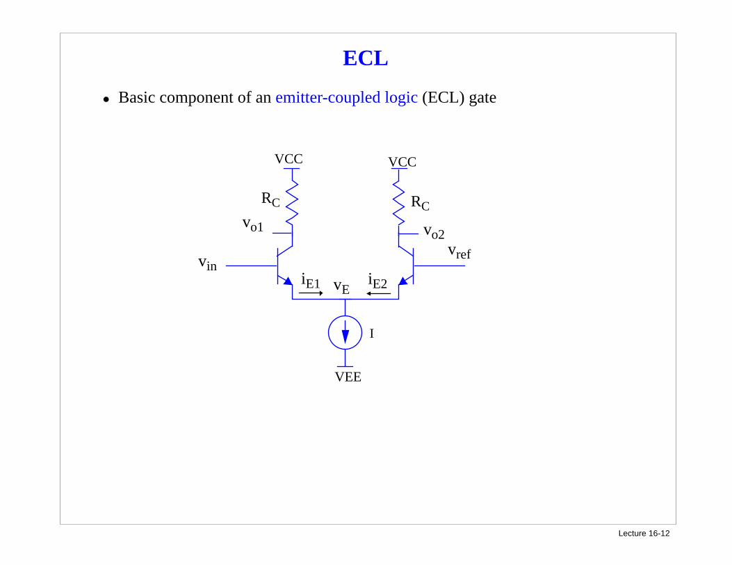
ECL
• Basic component of an emitter-coupled logic (ECL) gate
VCC
RC
vin
VCC
RC
vref
vo1 vo2
I
vE iE1 iE2
VEE
Lecture 16-13
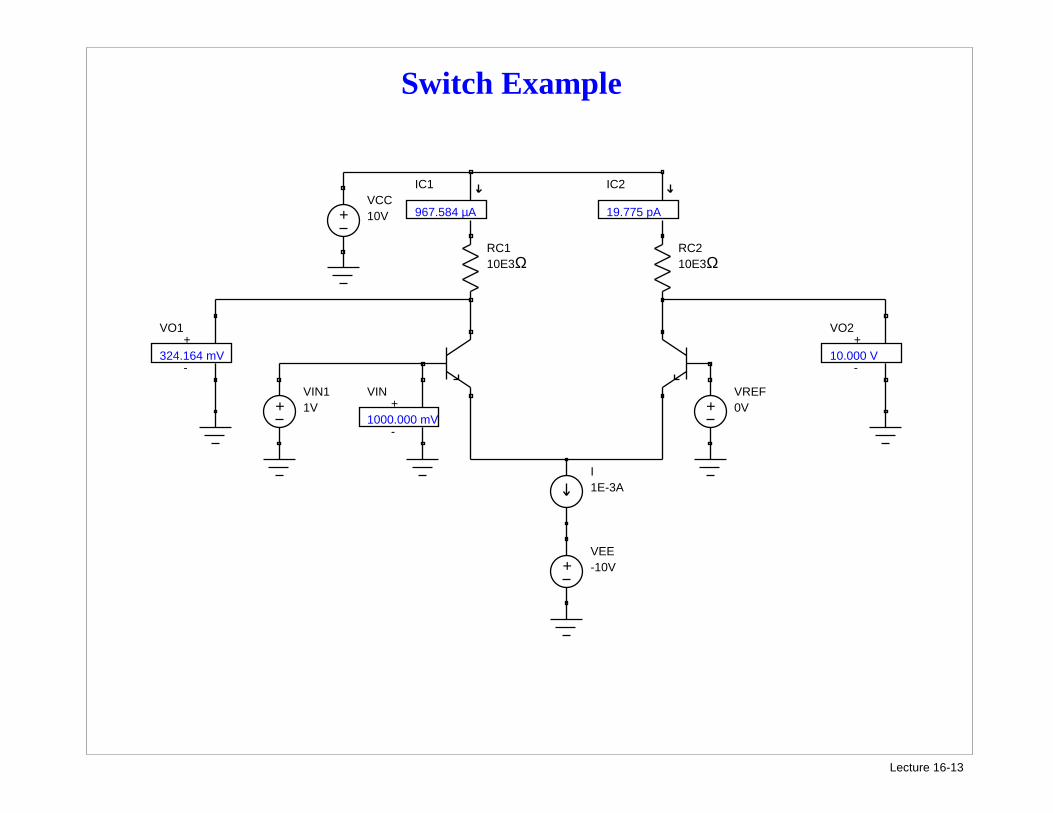
Switch Example
RC110E3Ω
+ 10VVCC
+
-
VO2
10.000 V
+ 0VVREF
RC210E3Ω
IC1
967.584 µA
+ -10VVEE
+
-
VIN
1000.000 mV
1E-3AI
IC2
19.775 pA
+
-
VO1
324.164 mV
+ 1VVIN1
Lecture 16-14
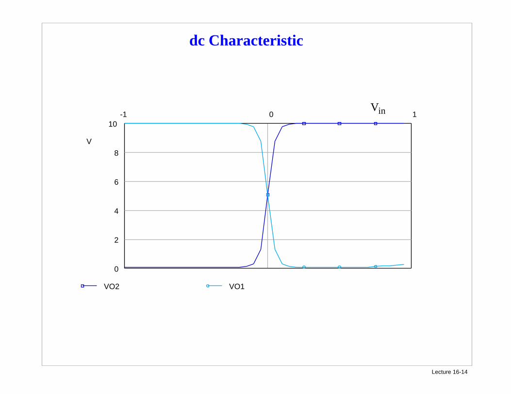
dc Characteristic
-1 0 1
0
2
4
6
8
10
V
VO2 VO1
Vin
Lecture 16-15
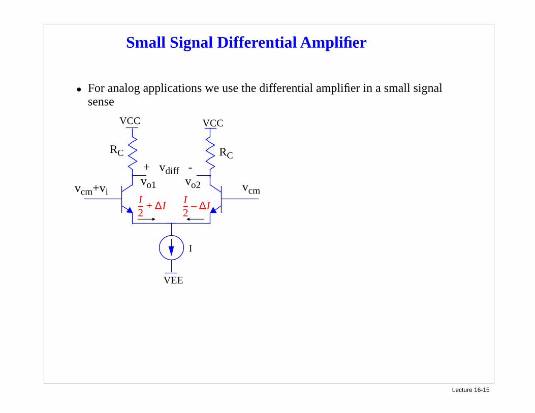
Small Signal Differential Amplifier
• For analog applications we use the differential amplifier in a small signal sense
VCC
RC
vcm+vi
VCC
RC
vcm vo1 vo2
I
VEE
+ vdiff -
I2--- ∆I+ I
2--- ∆I–
Lecture 16-16
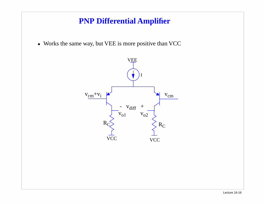
PNP Differential Amplifier
• Works the same way, but VEE is more positive than VCC
VCC
RC
vcm+vi
VCC
RC
vcm
vo1 vo2
I
VEE
- vdiff +
Lecture 16-17
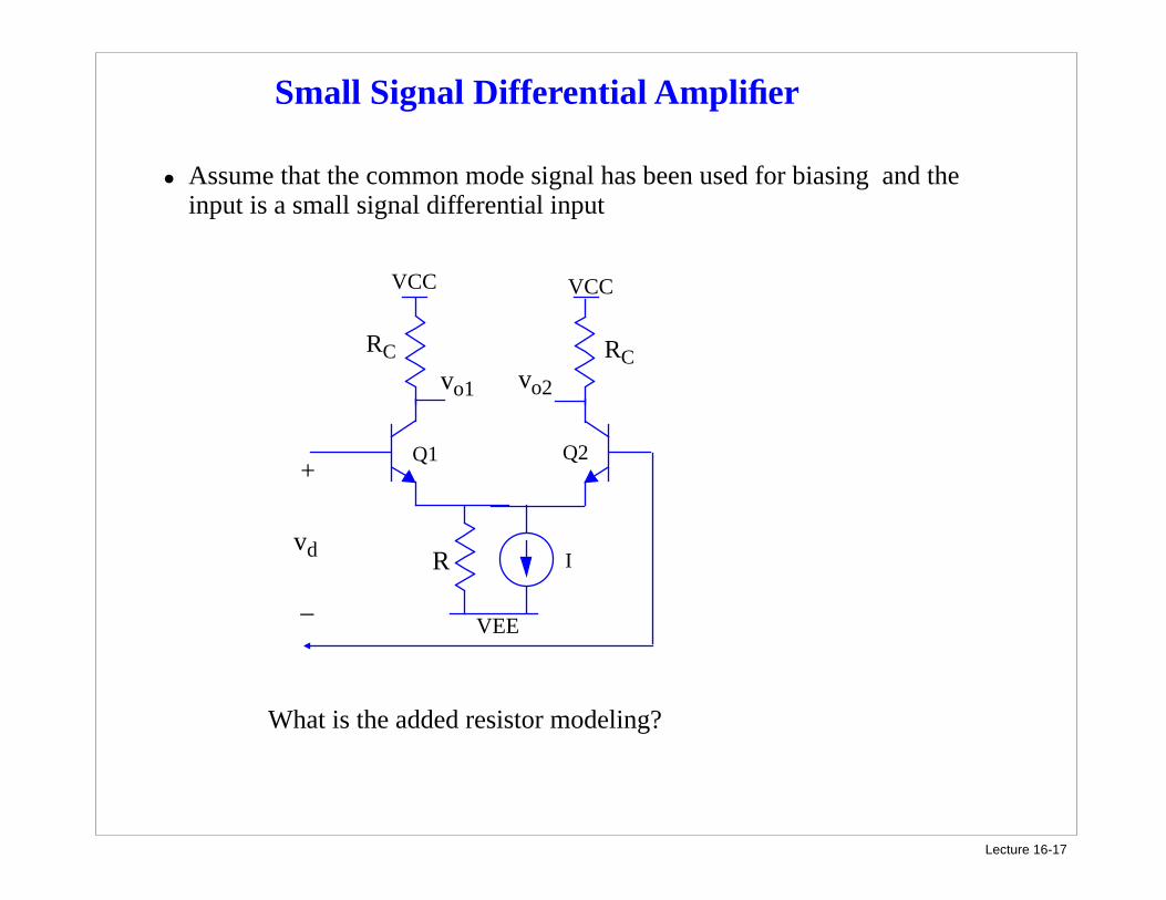
Small Signal Differential Amplifier
• Assume that the common mode signal has been used for biasing and the input is a small signal differential input
VCC
RC
vd
VCC
RC vo1 vo2
I
VEE
R
+
_
Q1 Q2
What is the added resistor modeling?
Lecture 16-18
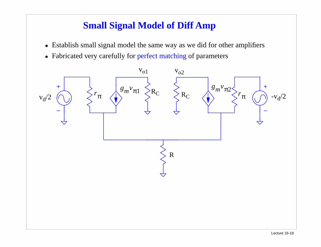
Small Signal Model of Diff Amp
• Establish small signal model the same way as we did for other amplifiers
• Fabricated very carefully for perfect matching of parameters
vd/2
vo1
RC -vd/2
gmvπ2
vo2
RC gmvπ1
R
rπ rπ
Lecture 16-19
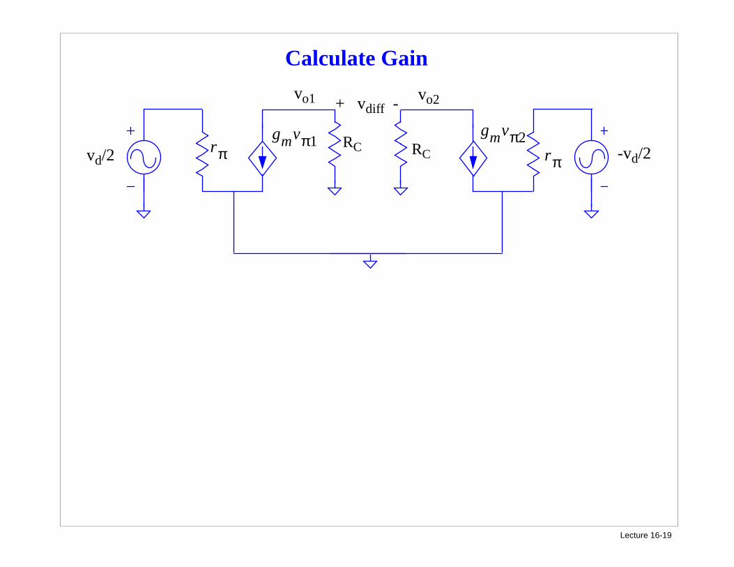
Calculate Gain
vd/2
vo1
RC -vd/2
gmvπ2
vo2
RC gmvπ1
+ vdiff -
rπ rπ
Lecture 16-20
Calculate Gain
vid/2
vo1
RC -vid/2
gmvπ2
vo2
RC gmvπ1
+ vdiff -
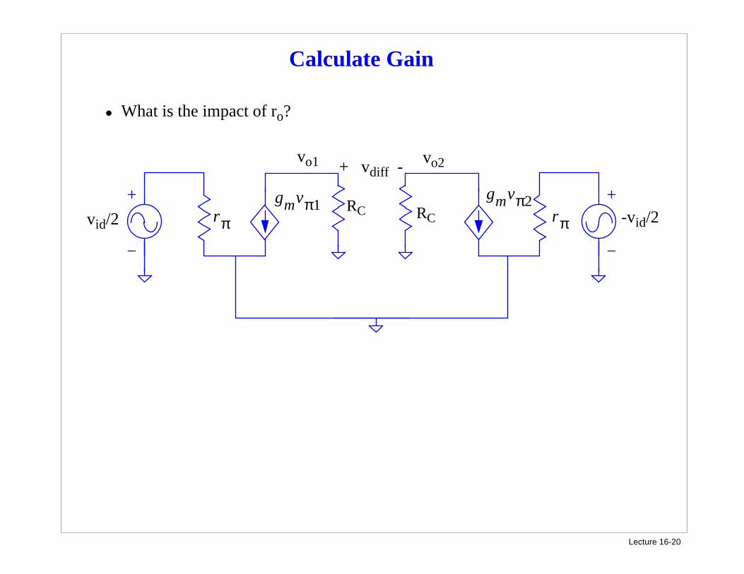
• What is the impact of ro?
rπ rπ
Lecture 16-21
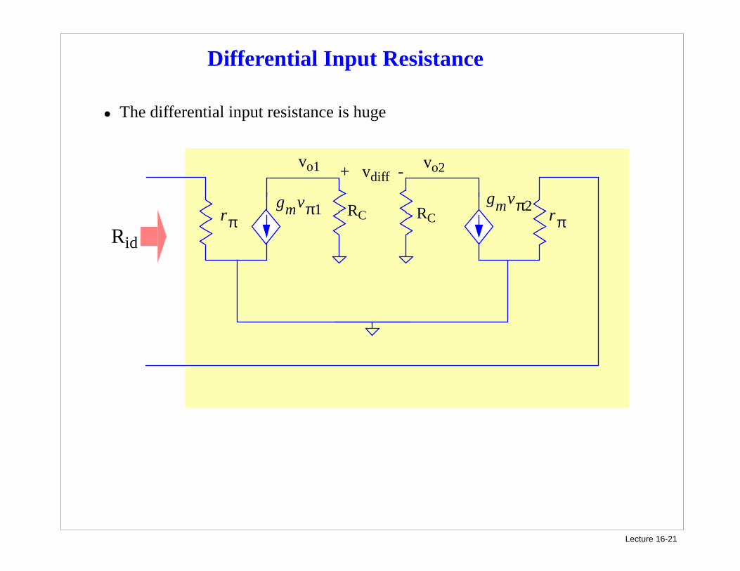
Differential Input Resistance
• The differential input resistance is huge
vo1
RC gmvπ2
vo2
RC gmvπ1
+ vdiff -
Rid
rπ rπ
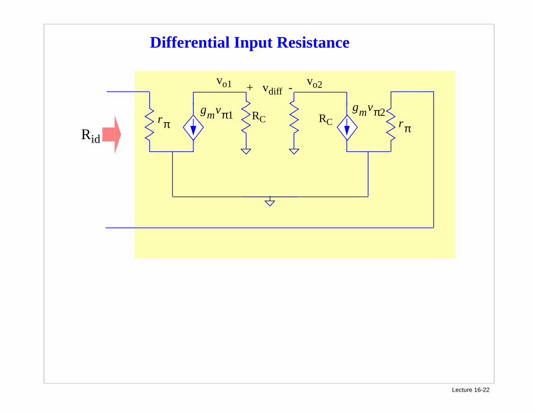
Lecture 16-22
Differential Input Resistance
vo1
RC gmvπ2
vo2
RC gmvπ1
+ vdiff -
Rid
rπ rπ
Lecture 16-23
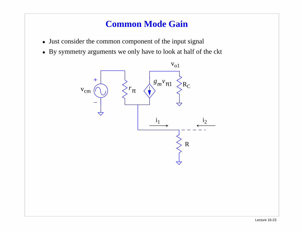
Common Mode Gain
• Just consider the common component of the input signal
• By symmetry arguments we only have to look at half of the ckt
vcm
vo1
RC gmvπ1
R
i1 i2
rπ
Lecture 16-24
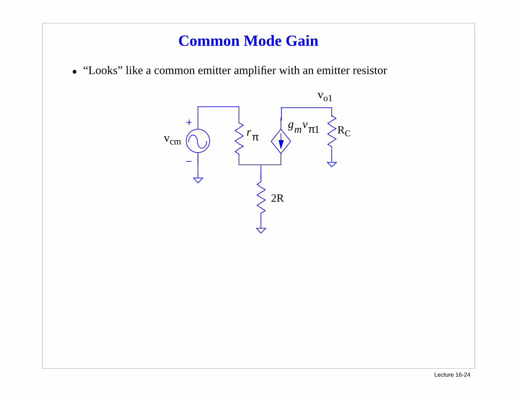
Common Mode Gain
• “Looks” like a common emitter amplifier with an emitter resistor
vcm
vo1
RC gmvπ1
2R
rπ
Lecture 16-25
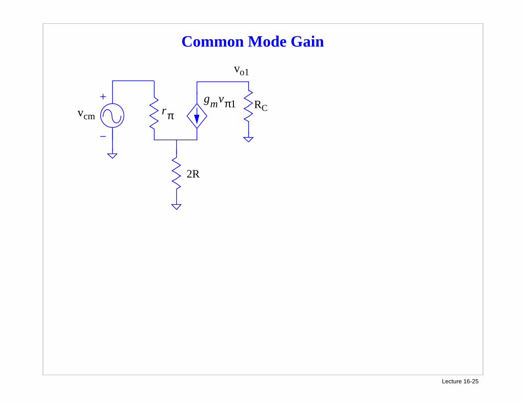
Common Mode Gain
vcm
vo1
RC gmvπ1
2R
rπ
Lecture 16-26
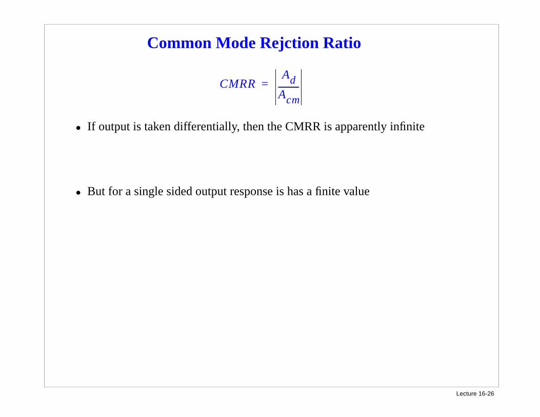
Common Mode Rejction Ratio
• If output is taken differentially, then the CMRR is apparently infinite
• But for a single sided output response is has a finite value
CMRRAd
Acm----------=
Lecture 16-27
Common Mode Rejction Ratio
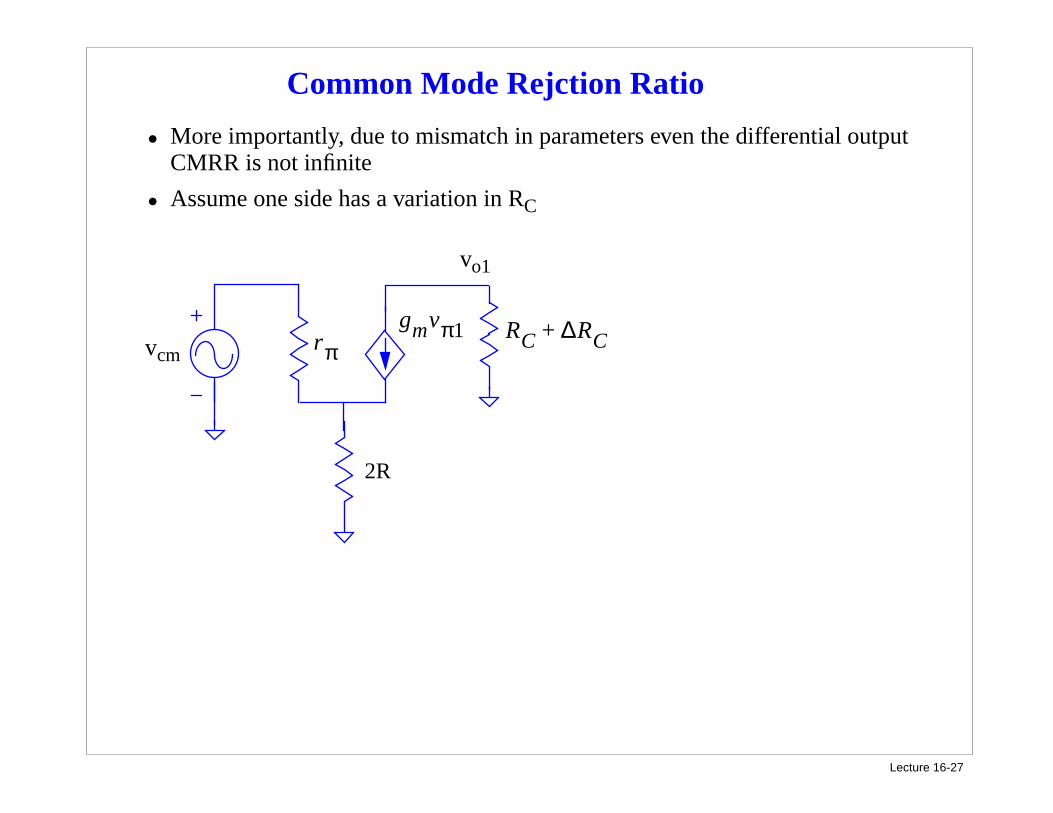
• More importantly, due to mismatch in parameters even the differential output CMRR is not infinite
• Assume one side has a variation in RC
vcm
vo1
gmvπ1
2R
rπRC ∆RC+
Lecture 16-28
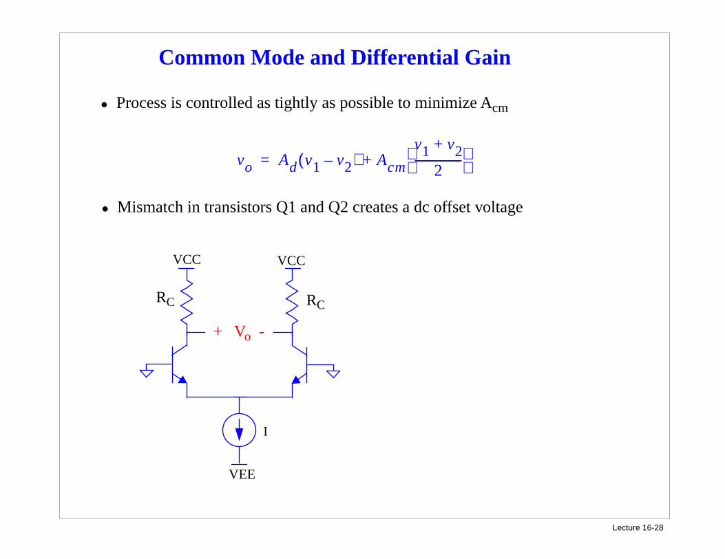
Common Mode and Differential Gain
• Process is controlled as tightly as possible to minimize Acm
vo Ad v1 v2–( ) Acm
v1 v2+
2-----------------
+=
• Mismatch in transistors Q1 and Q2 creates a dc offset voltage
VCC
RC
VCC
RC
I
VEE
+ Vo -
Lecture 16-29
Common Mode Characteristics
• Differential inputs (like opamps) have a common mode input resistance too --- see derivation in the book
• Also, there is an input bias current to both inputs
• When the transistors are not perfectly matched there will be a slight offset in these values