Embed Size (px)
Citation preview

IceCube
PMT HV Base Board
Engineering Requirements Document (ERD)
Version 2.2f (Draft)
Revisions:
Version 1.0 W. Stroewe 1.1 A. Karle 1.2 A. Karle July 29, 2002
2.0 N. Kitamura August 15, 2002 2.1a N. Kitamura September 13, 2002 2.1b N. Kitamura September 16, 2002 2.1c N. Kitamura September 25, 2002 2.2 N. Kitamura October 10, 2002 2.2a N. Kitamura October 24, 2002 2.2b N. Kitamura October 25, 2002 2.2c N. Kitamura November 15, 2002 2.2d N. Kitamura November 18, 2002 2.2e N. Kitamura November 21, 2002 2.2f N. Kitamura December 12, 2002
DRAFT PMTHVBaseERD_ver2.2f
Table of Contents Table of Contents..................................................................................................2 List of Figures .......................................................................................................3 List of Tables ........................................................................................................3 1 GENERAL ....................................................................................................4
1.1 Scope..................................................................................................4 1.2 Purpose...............................................................................................4 1.3 Precedence.........................................................................................4 1.4 Responsibilities ...................................................................................4 1.5 Records...............................................................................................4 1.6 Units....................................................................................................4 1.7 Glossary and Acronyms List ...............................................................4 1.8 References..........................................................................................6
2 FUNCTIONAL OVERVIEW ..........................................................................6 3 PERFORMANCE REQUIREMENTS............................................................9
3.1 The HV PMT Supply ...........................................................................9 3.1.1 General ........................................................................................9 3.1.2 Dynode Chain Voltage Distribution ..............................................9 3.1.3 Damping Resistor Requirements ...............................................10 3.1.4 HV Control .................................................................................10 3.1.5 Anode Current Sourcing Capability............................................11 3.1.6 Stability ......................................................................................11 3.1.7 Noise..........................................................................................11
3.2 Electrical ...........................................................................................12 3.2.1 Power.........................................................................................12 3.2.2 Ground.......................................................................................12 3.2.3 Anode Signal Connection Requirements ...................................13 3.2.4 PMT Mounting Holes Requirements ..........................................16 3.2.5 Digital Functionality Requirements.............................................18
3.3 Physical.............................................................................................21 3.3.1 Definition....................................................................................21 3.3.2 Overall size and shape requirements.........................................21 3.3.3 Component placement...............................................................22 3.3.4 Excluded area............................................................................22 3.3.5 Minimum trace spacing requirements ........................................22 3.3.6 Manual soldering compatibility ...................................................22
3.4 Environmental ...................................................................................23 3.4.1 Temperature Range...................................................................23 3.4.2 Pressure Range.........................................................................23
3.5 Miscellaneous ...................................................................................23 3.5.1 Conformal coating......................................................................23 3.5.2 Silkscreen ..................................................................................23
Appendix 1 Design Notes .............................................................................25
Page 2 of 27

DRAFT PMTHVBaseERD_ver2.2f
List of Figures Figure 2.1 Functional overview of the PMT HV Base board. ............................7 Figure 3.1 Split ground configuration requirement..........................................13 Figure 3.2 Anode signal coupling transformer signal definition (Illustration
purpose only. See text for correct winding requirements).............14 Figure 3.3 Plated-thru PMT mounting hole locations viewed from the top-side
of the PMT HV Base circuit board. The numerical labels associated with the holes mark the corresponding PMT pin number whose signal assignments are defined in Table 3.3. ................................16
Figure 3.4 Solder pad specification ................................................................17 Figure 3.5 Ribbon connector signal assignment.............................................20 Figure 3.7 PSL Drawing No. 5549B020. PMT HV Base Board dimensional
and component placement requirements. The figure identifies suggested locations for the ribbon cable connector, the coaxial cable attachment, and the clean ground wire attachment. The PCB material thickness is for reference only. (5549020B_e.pdf)..........24
Figure 3.8 PSL Drawing No. 5549C021. PMT HV Base Board component envelope definition. (5549021C_e.pdf)..........................................24
List of Tables Table 2.1 Summary of electrical connections requirements ............................8 Table 3.1 Dynode chain voltage distribution (“Dyn” denotes the n-th dynode
or Dynode n. “Fn” denotes the n-th focusing electrode.) ..............10 Table 3.3 PMT Pin Assignment .....................................................................18 Table 3.4 Power ON/OFF signal assignment ................................................20 Table 3.6 Ribbon connector signal assignment.............................................21
Page 3 of 27
DRAFT PMTHVBaseERD_ver2.2f
1 GENERAL 1.1 Scope
This IceCube Engineering Requirements Document (ERD) specifies the physical, functional and performance requirements for the PMT High Voltage Base circuit board.
1.2 Purpose This requirement documentation shall be applicable to the development, prototyping, testing, and verification of the PMT High-Voltage Base circuit board.
1.3 Precedence In the event of a conflict between the provisions of this document and any prior IceCube documents, the provisions of this document shall govern. Conflicts with other documents are resolved by the Change Control Board.
1.4 Responsibilities 1.4.1 Physics/Engineering is responsible for writing and updating
these requirements to ensure they are correct, complete and current.
1.4.2 Quality Assurance is responsible for ensuring this document and changes to it are properly reviewed, approved and maintained.
1.5 Records Records of initial review, approval and changes (Engineering Change Notices, ECN’s) in design shall be maintained according to the established processes.
1.6 Units Weights and measures in this document are expressed in the MKS International System of Units (SI).
1.7 Glossary and Acronyms List ADC Analog-to-Digital Converter AWG American Wire Gauge cm Centimeter CMOS Complementary Metal Oxide Semiconductor CS0 Chip-select bit 1 CS1 Chip-select bit 0 DAC Digital-to-Analog Converter DAQ Data Acquisition System DC Direct Current
Page 4 of 27

DRAFT PMTHVBaseERD_ver2.2f
DOM Digital Optical Module DOMMB Digital Optical Module Main Board ERD Engineering Requirements Document HV High Voltage Hz Hertz IDC Insulation Displacement Connector IPC Institute for Interconnecting and Packaging Electronic
Circuits k Kilo (103) kg Kilogram LED Light-Emitting Diode MKS Meter-kilogram-second M Mega (106) m Meter mA Milliampere MOSI Master-Out-Slave-In MISO Master-In-Slave-Out mV Millivolt mW Milliwatt n Nano (10-9) OD Outside Diameter OM Optical Module Pa Pascal PCB Printed Circuit Board PE Photoelectron pF Pico Farad PMT Photomultiplier Tube P/N Part Number PSL Physical Sciences Laboratory, University of
Wisconsin-Madison P/V ratio Peak-to-valley ratio s, sec Second SCLK Serial Clock SI Système International d’Unités SPE Single Photoelectron TBD To Be Determined UL Underwriters Laboratory V Volt VDC Volt DC
Page 5 of 27
DRAFT PMTHVBaseERD_ver2.2f
W Watt
1.8 References • IceCube DOM Main Board – PMT HV Base Board Interface
Requirements (Document No. 9000-0006) • DOM Main Board Hardware Requirements (Document No.
9000-0007) • PSL Drawing No. 5549B020 (PMT HV Base Circuit Board) • PSL Drawing No. 5549C021 (PMT Envelope) • IPC-2221 (Generic Standard on Printed Board Design)
2 FUNCTIONAL OVERVIEW The photo-multiplier tube high-voltage base (PMT HV Base) board is a modular PCB component to be integrated into each of the approximately 5000 optical modules (OM), containing a photo-multiplier tube (PMT), that will be deployed in the Antarctic deep-ice (below several kilometers) for scientific research purposes. The PMT referred to in this document is a Hamamatsu Model 7081-02 with a nominal size of 10 inches (25.4 cm) in diameter and a nominal gain of 108. The PMT HV Base board is required to function continuously without service over the entire twenty-year span of the research project under the deep-ice condition. The operating temperature of the PMT HV Base board is a function of the deployment depth of the Optical Module in the ice, ranging roughly from –20°C to –40°C, whereas the operating pressure is that of the internal pressure of the OM, approximating the Antarctic ambient pressure of ~0.5 atm. See 3.4 Environmental. The PMT HV Base board has physical and electrical connections inside the OM with the photo-multiplier tube (PMT) and the digital optical module (DOM) main board (MB), the latter serving as the master controller of the entire OM. Figure 2.1 depicts the functional relationship among the PMT HV Base board, the DOMMB and the PMT. Table 2.1 summarizes the electrical connections between the PMT HV Base Board and the DOM Main Board. The purpose of the PMT HV Base board is to facilitate the following functions:
1. Generate a series of high-voltages for the individual dynodes,
focusing electrodes and the anode of the PMT, using the power provided by the DOMMB.
Page 6 of 27

DRAFT PMTHVBaseERD_ver2.2f
2. Transfer the anode signal pulses from the PMT to the DOMMB without distortion through a coaxial cable.
3. Respond to the digital control commands issued by the DOMMB for power on/off and for the adjustment of the high voltages.
4. Provide a digital reading of the high voltage to the DOMMB upon request.
5. Provide digital board identification information to the DOMMB upon request.
The mechanical installation of the PMT HV Base board is accomplished by inserting the PMT lead pins into the plated-thru holes arranged on the PCB and soldering the pins to the annular pad associated with each plated-thru hole; this procedure also establishes the electrical connections between the PMT and the PMT HV Base board. Detailed functional and performance requirements are specified in the rest of the document.
Figure 2.1 Functional overview of the PMT HV Base
board.
Page 7 of 27
DRAFT PMTHVBaseERD_ver2.2f
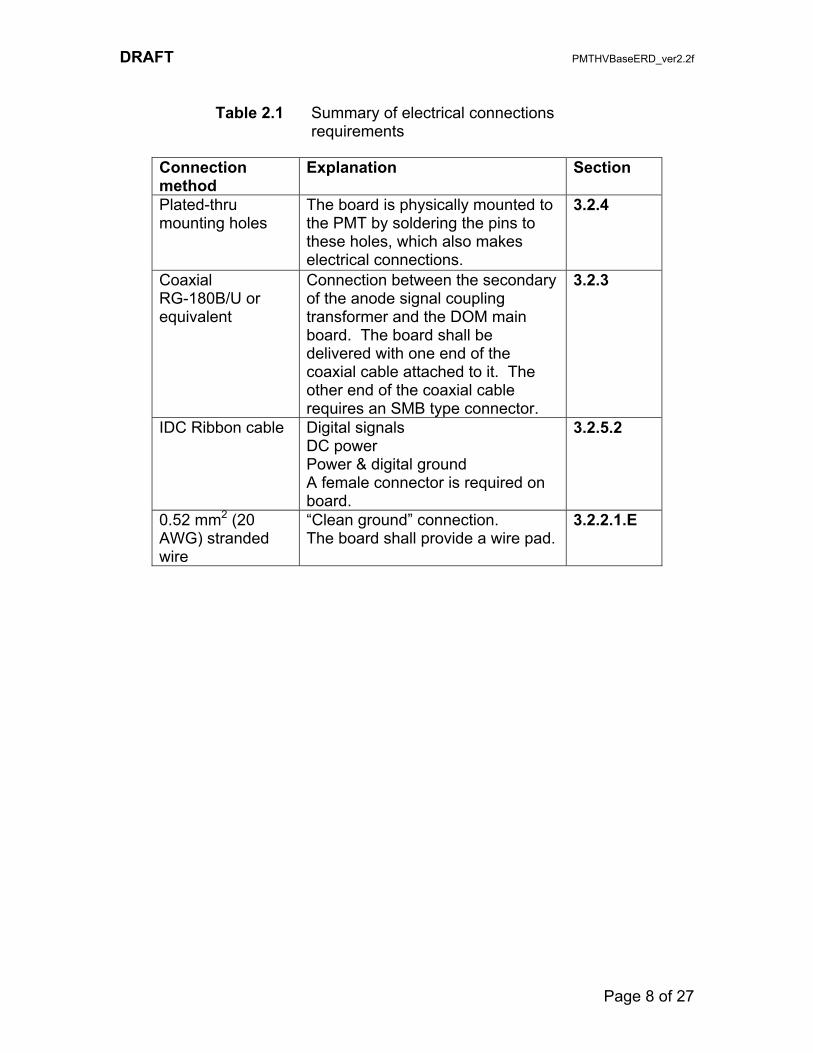
Table 2.1 Summary of electrical connections requirements
Connection method
Explanation Section
Plated-thru mounting holes
The board is physically mounted to the PMT by soldering the pins to these holes, which also makes electrical connections.
3.2.4
Coaxial RG-180B/U or equivalent
Connection between the secondary of the anode signal coupling transformer and the DOM main board. The board shall be delivered with one end of the coaxial cable attached to it. The other end of the coaxial cable requires an SMB type connector.
3.2.3
IDC Ribbon cable
Digital signals DC power Power & digital ground A female connector is required on board.
3.2.5.2
0.52 mm2 (20 AWG) stranded wire
“Clean ground” connection. The board shall provide a wire pad.
3.2.2.1.E
Page 8 of 27

3 PERFORMANCE REQUIREMENTS 3.1 The HV PMT Supply
3.1.1 General This subsection specifies electrical requirements applicable to the HV PMT supply portion of the PMT HV Base Board.
3.1.1.1 Note on requirements alternatives A set of alternative requirements, replacing the requirements defined in Section 3.1.4, shall be issued at a later date as a supplement to this ERD. The vendor of the PMT HV Base board shall be appropriately notified by IceCube as to whether the present requirements or the said alternative requirements are to be enforced.
3.1.1.2 HV Generation The method of HV generation shall be compatible with all the requirements stated in this document. In particular, the electrical impedance of the voltage sources for the individual dynodes must be sufficiently low in order to meet the anode current sourcing capability (3.1.5).1
3.1.1.3 Definition (a) “First dynode voltage” shall refer to the voltage between
the cathode and the first dynode of the PMT. (b) “Anode voltage” shall refer to the voltage between the first
dynode and the anode of the PMT. 3.1.2 Dynode Chain Voltage Distribution2 3.1.2.1 Dynodes
The voltage across the successive dynode stages shall be according to the values specified in Table 3.1 in which the values are expressed in terms of a factor to be multiplied by the voltage across Dynode 1 (first dynode) and Dynode 2.
3.1.2.2 Focusing electrodes The voltage for the focusing electrodes, denoted as F1 – F3, shall also be determined by the factor specified in Table 3.1 multiplied by the voltage across Dynode 1 and Dynode 2.
Note: F1 and Dy1 are at the same potential. F2 and F3 are at the same potential.

DRAFT PMTHVBaseERD_ver2.2f
3.1.3 Damping Resistor Requirements 3.1.3.1
A 100Ω (5% or better) resistor shall be present between each one of the last dynodes (Dy8, Dy9 and Dy10) and the corresponding high-voltage sources.
3.1.3.2 The said damping resistors shall be installed at locations easily accessible for the IceCube engineers to shunt or replace after the PMT HV Base board has been mounted on the PMT.
Table 3.1 Dynode chain voltage distribution (“Dyn”
denotes the n-th dynode or Dynode n. “Fn” denotes the n-th focusing electrode.) Interval Voltage relative
to Dy1 - Dy2 Dy2 - Dy3 1.25 Dy3 - Dy4 0.83 Dy4 - Dy5 0.42 Dy5 - Dy6 0.25 Dy6 - Dy7 0.30 Dy7 - Dy8 0.38 Dy8 - Dy9 0.55 Dy9 - Dy10 0.75
Dy1 - F1 0.15 Dy1 - F2 0 Dy1 - F3 0.15
3.1.4 HV Control 3.1.4.1 HV controllability requirements 3.1.4.1.A First dynode voltage
(a) The first dynode voltage shall be set to the factory default value of 700 VDC.
(b) There shall be a provision for changing the said factory default value after delivery by the IceCube personnel to a value in the range of 600 to 800 VDC, using a readily-accessible and reliable method, such as installing or replacing a resistor.
3.1.4.1.B Anode voltage The anode voltage (first dynode-to-anode voltage) shall be adjustable at least over the range of 1000 to 2000 VDC by
Page 10 of 27
DRAFT PMTHVBaseERD_ver2.2f
means of a suitable digital code written to the DAC residing on the PMT HV Base board.3
3.1.4.2 HV monitoring requirement There shall be a provision for monitoring the cathode-to-anode voltage as a digital code of an ADC reading transmitted to the DOM main board.4
3.1.4.3 Digital interface 3.1.4.3.A DAC resolution
The DAC used for setting the HV shall have a resolution of 12-bit.
3.1.4.3.B ADC resolution The ADC used for monitoring the HV shall have resolution of 12-bit.
3.1.4.3.C Digital code vs HV5 (a) The digital code for setting and monitoring the HV shall
be in 12-bit unsigned straight binary with the digital value 000(hex) representing 0 V.
(b) The digital value and the corresponding HV value shall have a linear relationship at least in the voltage range specified in 3.1.4.1 with the slope of 0.5 V per bit.
3.1.5 Anode Current Sourcing Capability6 The HV generator of the PMT HV Base board shall support the following current sourcing capability in the sense that the output voltage does not drop more than 10 V while producing the specified current:
(a) DC anode current of 12 nA at –40 °C (deep-ice). (b) DC anode current of 240 nA at room temperature
(laboratory). (c) Square-pulse anode current of 100 mA lasting for 1 µsec.
3.1.6 Stability The drift rate for the voltages supplied to the dynodes and the anode shall be less than 4 V / week during the regular in-ice operation.7
3.1.7 Noise The ripple voltage observed at the output of the secondary of the anode signal-coupling transformer shall be no greater than 0.5mVpp when the output is terminated with a 100 Ω resistor.8
Page 11 of 27
DRAFT PMTHVBaseERD_ver2.2f
3.2 Electrical 3.2.1 Power 3.2.1.1
The PMT HV Base circuit board shall receive the electrical power from the DOM Main Board through the ribbon cable connector specified in 3.2.5.2.
3.2.1.2 The power source available to the PMT HV Base circuit board shall be a ±5 VDC voltage source with a voltage uncertainty of ±5%.
3.2.1.3 The maximum power dissipation of the PMT HV Base board shall be 150 mW.
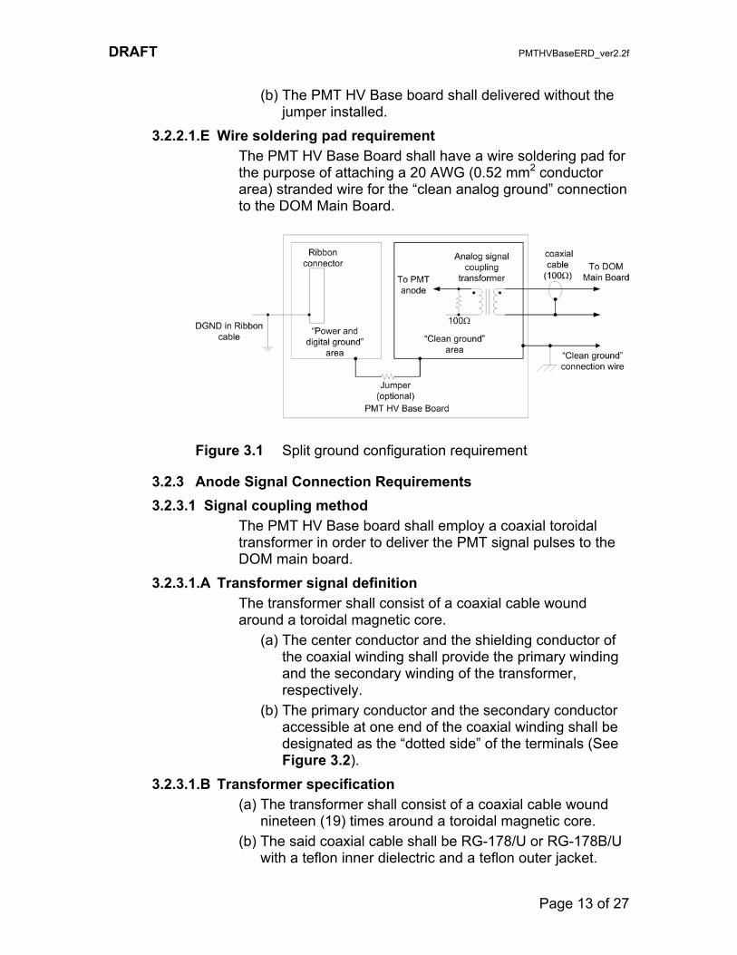
3.2.2 Ground 3.2.2.1 Split ground configuration 3.2.2.1.A Definitions
The PMT HV Base board shall have two isolated ground planes as defined below (See Figure 3.1):
(a) Digital and power ground shall be referenced by the incoming power from the DOM Main Board; the digital control and monitor circuitry including the ADC and the DAC; and, the regulator and switching circuitry for HV generation.
(b) Clean analog ground shall be referenced by the voltage multiplier, dynode resistive divider, and regulator feedback circuitry.
3.2.2.1.B Isolation resistance The two ground planes defined above shall have a minimum isolation resistance of 10 MΩ.
3.2.2.1.C Stray capacitance The stray capacitance between the two ground planes shall be less than 50 pF.
3.2.2.1.D Jumper requirement The PMT HV Base board shall have solder pads for a solderable jumper (a zero-ohm resistor) between the two ground planes.
(a) The installation of the jumper is optional and shall be decided by the IceCube engineers after the delivery.9
Page 12 of 27
DRAFT PMTHVBaseERD_ver2.2f
(b) The PMT HV Base board shall delivered without the jumper installed.
3.2.2.1.E Wire soldering pad requirement The PMT HV Base Board shall have a wire soldering pad for the purpose of attaching a 20 AWG (0.52 mm2 conductor area) stranded wire for the “clean analog ground” connection to the DOM Main Board.
Figure 3.1 Split ground configuration requirement
3.2.3 Anode Signal Connection Requirements 3.2.3.1 Signal coupling method
The PMT HV Base board shall employ a coaxial toroidal transformer in order to deliver the PMT signal pulses to the DOM main board.
3.2.3.1.A Transformer signal definition The transformer shall consist of a coaxial cable wound around a toroidal magnetic core.
(a) The center conductor and the shielding conductor of the coaxial winding shall provide the primary winding and the secondary winding of the transformer, respectively.
(b) The primary conductor and the secondary conductor accessible at one end of the coaxial winding shall be designated as the “dotted side” of the terminals (See Figure 3.2).
3.2.3.1.B Transformer specification (a) The transformer shall consist of a coaxial cable wound
nineteen (19) times around a toroidal magnetic core. (b) The said coaxial cable shall be RG-178/U or RG-178B/U
with a teflon inner dielectric and a teflon outer jacket.
Page 13 of 27

DRAFT PMTHVBaseERD_ver2.2f
(c) The said toroidal magnetic core shall be Magnetics Model ZH-42206-TC (www.mag-inc.com) or equivalent.
(d) Adequate spacing between the windings shall be provided in order to insure high-voltage isolation integrity.
(e) There shall be an adequate means to hold the windings in place (such as a plastic plug pressed into the toroidal center, or a “belly-band” around the transformer).
3.2.3.1.C Primary side requirements10 (a) The primary side of the coaxial transformer shall be
terminated with a 100Ω resister across the primary terminals (“back termination”).
(b) The “dotted” side of the primary terminal shall connect to the PMT anode terminal.
(c) The “un-dotted” side of the primary terminal shall connect to the source of the anode high-voltage.
3.2.3.1.D Secondary side requirements11 (a) The secondary side of the coaxial transformer shall be
connected to the DOM Main Board using a coaxial medium.
(b) The said coaxial medium shall be RG-180B/U or a similar coaxial cable with a characteristic impedance of 100Ω.
(c) The center conductor and the shield conductor of the said coaxial cable shall connect to the “dotted” side and the “un-dotted” side of the secondary terminal of the transformer, respectively.
Figure 3.2 Anode signal coupling transformer signal
definition (Illustration purpose only. See text for correct winding requirements).
3.2.3.1.E Coaxial cable installation requirement
The PMT HV Base Board shall be delivered with the coaxial cable specified in 3.2.3.1.D installed.
Page 14 of 27

DRAFT PMTHVBaseERD_ver2.2f
(a) Electrical connections of the coaxial cable shall be accomplished by direct soldering.12
(b) The said electrical connections shall not degrade when the cable is pulled with a maximum of 5kg of force in any directions.
(c) The length of the coaxial cable shall be 20 ±1cm. (d) The end of the said coaxial cable not attached to the
PCB shall have a right-angle, crimp-type SMB connector.
Page 15 of 27

DRAFT PMTHVBaseERD_ver2.2f
3.2.4 PMT Mounting Holes Requirements 3.2.4.1 Plated-thru PMT mounting holes and soldering pads 3.2.4.1.A
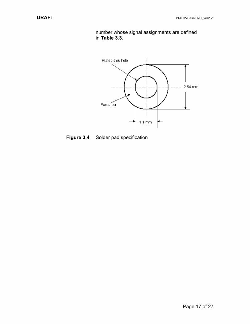
The PMT HV Base board shall have plated-thru holes specified in Figure 3.3 in order to make electrical connections to the PMT.
3.2.4.1.B Each of the said plated-thru holes shall have an annular soldering pad in the manner specified in Figure 3.4.
3.2.4.1.C The locations of the said plated-thru holes on the PCB are as specified in Figure 3.7.
3.2.4.2 Signal assignment to the PMT mounting holes13 3.2.4.2.A
The electrical signal assignment to the plated-thru PMT mounting holes are as shown in Figure 3.3 and Table 3.3.
3.2.4.2.B The PMT HV Base board shall not be required to have holes to accommodate the pins that are assigned “No connection”.
Figure 3.3 Plated-thru PMT mounting hole locations
viewed from the top-side of the PMT HV Base circuit board. The numerical labels associated with the holes mark the corresponding PMT pin
Page 16 of 27
DRAFT PMTHVBaseERD_ver2.2f
number whose signal assignments are defined in Table 3.3.
Figure 3.4 Solder pad specification
Page 17 of 27

DRAFT PMTHVBaseERD_ver2.2f
Table 3.3 PMT Pin Assignment Pin # Signal name Description
01 NC No connection 02 Dy1 Dynode #1 03 F3 Focus #3 04 NC No connection 05 Dy3 Dynode #3 06 NC No connection 07 Dy5 Dynode #5 08 Dy7 Dynode #7 09 Dy9 Dynode #9 10 P Anode 11 NC No connection 12 NC No connection 13 NC No connection 14 Dy10 Dynode #10 15 Dy8 Dynode #8 16 Dy6 Dynode #6 17 Dy4 Dynode #4 18 NC No connection 19 Dy2 Dynode #2 20 F1 Focus #1 21 F2 Focus #2 22 NC No connection 23 NC No connection 24 K Cathode
3.2.5 Digital Functionality Requirements 3.2.5.1 Digital signal standard 3.2.5.1.A The digital signals (logic levels and voltages) between the PMT
HV Base board and the DOM main board shall comply with the 3V CMOS signal standard.
3.2.5.1.B The PMT HV Base Board shall not rely on the 5V-tolerance of the DOM Main Board when transmitting a signal.
3.2.5.2 The ribbon cable The PMT HV Base Board shall have electrical connections with the DOM Main Board through a ribbon cable, defined in this section, for the following purposes:
• Power and ground connections • Digital signal connections
Page 18 of 27
DRAFT PMTHVBaseERD_ver2.2f
3.2.5.2.A The ribbon cable type The ribbon cable shall be a 1.27mm-pitch flat IDC ribbon cable.
3.2.5.2.B The ribbon connector type14 The PMT HV Base board shall have a 2.54mm-pitch female IDC-type connector for the ribbon cable at the location specified in Figure 3.8. The said connector shall be an AMP Micro-MaTch top-entry receptacle with locking (Tyco Electronics P/N 2-338068-0).
3.2.5.2.C Signal duplication requirement Each signal, ground and power in the ribbon cable shall have two connector pins allocated to it.
3.2.5.2.D Ribbon connector signal assignment The signal assignment to the ribbon connector pins shall be as defined in Table 3.6.
3.2.5.3 Chip-select (CS0, CS1) The two chip-select signals, CS0 and CS1, shall be used in combination to select one of the following three digital devices residing on the PMT HV Base board:
• DAC: Digital-to-analog converter • ADC: Analog-to-digital converter • IDENT: Board identification device (3.2.5.6)
3.2.5.3.A The assignment of the logic levels to CS0 and CS1 shall be determined by the vendor of the PMT HV Base board.
3.2.5.4 MOSI, MISO and SCLK signals • DAC shall use MOSI and SCLK for data and serial
clock, respectively. • ADC shall use MISO and SCLK for data and serial
clock, respectively. • IDENT shall use one or more of MOSI, MISO and
SCLK. 3.2.5.5 Power ON/OFF Control 3.2.5.5.A
The PMT HV Base board shall support a power ON/OFF control by the DOM Main Board through the ribbon cable.
3.2.5.5.B ON/OFF control signal The signal assignment for the power ON/OFF control shall be as shown in Table 3.4.
Page 19 of 27

DRAFT PMTHVBaseERD_ver2.2f
3.2.5.5.C Power-up default When the PMT HV Base board is turned on, the HV output shall be consistent with the DAC digital code of 0x000 (See 3.1.4.3.A).
Table 3.4 Power ON/OFF signal assignment
Logic Level Meaning 0 OFF 1 ON
3.2.5.6 Digital Board Identification 3.2.5.6.A
The PMT HV Base board shall provide a unique digital board identification number (board ID) upon request from the DOM main board.
3.2.5.6.B The said digital board ID device shall comply with the Dallas 1-Wire protocol to communicate with DOMMB serving as the bus master.15
(Board edge)
Figure 3.5 Ribbon connector signal assignment
Page 20 of 27

DRAFT PMTHVBaseERD_ver2.2f
Table 3.6 Ribbon connector signal assignment Pin # Signal Name Description
01 DGND Digital and power ground 02 SCLK Serial clock 03 SCLK 04 MOSI Master-out-slave-in 05 MOSI 06 MISO Master-in-slave-out 07 MISO 08 DGND 09 CS0 Chip-select bit 0 (See ) 10 CS0 11 CS1 Chip-select bit1 (See ) 12 CS1 13 ON/OFF Board enable/disable 14 ON/OFF 15 +5V Main power (+) 16 +5V 17 DGND 18 DGND 19 -5V Main power (-) 20 -5V
3.3 Physical 3.3.1 Definition
The “bottom side” of the PMT HV Base board shall refer to the side of the PCB from which the PMT leads are inserted. The “top side” of the PMT HV Base board shall refer to the side opposite to the bottom side. The terms “top view” and “bottom view” shall refer to the views from the top side and the bottom side of the PMT HV Base board, respectively.
Note: The “ice top view” is a view of the Optical Module components in ice seen from the ice top. For the purpose of the PMT HV Base board, the “ice top view” and the “top view” are synonymous.16
3.3.2 Overall size and shape requirements17 The overall shape of the printed circuit board of the PMT HV Base shall be circular and no larger than 100 mm in diameter. A greater diameter or a deviation from the circular outline for accommodation of special components such as connectors and cable harnesses shall be permitted provided that there is sufficient clearance between such components and the interior surface of the pressure vessel of the optical module. The dimensional requirements are
Page 21 of 27
DRAFT PMTHVBaseERD_ver2.2f
summarized in Figure 3.7 and Figure 3.8. The volume constraints shall apply to both of the mating pieces of the ribbon connectors.
3.3.3 Component placement The components may be placed on either the top side or the bottom side of the PCB within the constraints of the component envelope, except for the following items, whose locations are specified in Figure 3.8:
(a) Anode signal coupling transformer (Bottom side) (b) Coaxial cable for the anode signal connection (c) Ribbon cable connector (Bottom side.) (d) “Clean ground” connection wire pad
The following items shall be installed at locations where IceCube engineers can easily access for modification after the PMT HV Base board has been mounted on the PMT:
(e) Components for adjusting the first dynode voltage (3.1.4.1.A)
(f) Damping resistors (3.1.3) (g) Solder pads for the optional jumper (3.2.2.1.D)
3.3.4 Excluded area No components shall be mounted in the areas so specified in Figure 3.8.
3.3.5 Minimum trace spacing requirements18 In compliance with the circuit board trace layout rules specified for “B-4 External Conductors with Permanent Polymer Coating” in IPC-2221, §6.3 Electrical Clearance, the following conditions shall be met for both DC voltages and AC peak voltages:
• For voltage difference greater than 100 V and less than 300 V, the minimum trace spacing shall be 0.4 mm.
• For voltage difference greater than 300 V and less than 500 V, the minimum trace spacing shall be 0.8 mm.
• For voltage difference greater than 500 V, the minimum trace spacing shall be 0.8 mm plus 0.00305 mm per every volt exceeding 500 V.
3.3.6 Manual soldering compatibility19 The PCB shall be compatible with the increased temperature during the manual soldering of the PMT pins at the solder pads specified in 3.2.4.
Page 22 of 27

DRAFT PMTHVBaseERD_ver2.2f
3.4 Environmental 3.4.1 Temperature Range20 3.4.1.1 Operation
The continuous operating temperature of the PMT HV Base board shall be in the range of –40°C to +27°C.
3.4.1.2 Storage The storage temperature for the PMT HV Base board shall be in the range of –55°C to +45°C.
3.4.1.3 Component selection 3.4.1.3.A
To the extent practical, all the components used for the PMT HV Base board shall meet the lowest operating temperature of –55°C or lower, as specified by the component manufacturer, where “practical” means that this requirement applies to all resistors, capacitors and diodes; PCB material; conformal coating; and any other components that are readily available for the operating temperature of –55°C or lower.
3.4.1.3.B The vendor of the PMT HV Base board shall supply IceCube with a list of components used that do not meet the –55°C or lower operating temperature.
3.4.2 Pressure Range The PMT HV Base circuit board shall be capable of operating continuously inside the pressure vessel with the sustained internal pressure of 40,000 Pa to 100,000 Pa.
3.5 Miscellaneous 3.5.1 Conformal coating
Conformal coating is required on both sides of the PCB. 3.5.1.1 Masking requirement
Areas where soldering will be performed after delivery shall be properly masked from the conformal coating.
3.5.2 Silkscreen Silkscreen marking is required on the top side of the PCB.
3.5.2.1 Items to be identified The said marking shall at least identify the following items:
• Component(s) for setting the first dynode voltage
Page 23 of 27
DRAFT PMTHVBaseERD_ver2.2f
• Plated-thru holes for PMT connection • Solderable jumper • Clean ground wire pad
Figure 3.7 PSL Drawing No. 5549B020. PMT HV Base
Board dimensional and component placement requirements. The figure identifies suggested locations for the ribbon cable connector, the coaxial cable attachment, and the clean ground wire attachment. The PCB material thickness is for reference only. (5549020B_e.pdf)
Figure 3.8 PSL Drawing No. 5549C021. PMT HV Base
Board component envelope definition. (5549021C_e.pdf)
Page 24 of 27
DRAFT PMTHVBaseERD_ver2.2f
Page 25 of 27
Appendix 1 Design Notes
3.1.1.2 HV Generation
1 Justification: Reference to a Cockroft-Walton type generator in the earlier versions of this document has been removed in order to avoid unnecessary constraints on sound technical solutions.
3.1.2 Dynode Chain Voltage Distribution2 Note: The voltage ratios are in accordance with the specification for Hamamatsu PMT Model R7081-02.
3.1.4.1 HV controllability requirements3 Justification: The first dynode voltage mainly controls the peak-to-valley ratio (P/V ratio), whereas the anode voltage mainly controls the gain of the PMT. Once the first dynode voltage is set to a value corresponding to an adequate P/V ratio (greater than 2.2), the voltage should not require readjustment. It is possible to set the first dynode voltage to be sufficiently high so that the P/V ratio always exceeds the minimum required value of 2.2, regardless of the parameter variations among the PMTs. The PMT (Hamamatsu R7081-02) has a nominal operating voltage of 460V for the first dynode voltage. The manufacturer of the PMTs, however, confirms that the first dynode voltage may be as high as 800V without adverse effects. See the e-mail exchange between Kael Hanson and Yuji Yoshizawa, Application and Sales Engineer of Hamamatsu Photonics Electron Tube Center. The latest correspondence from Yoshizawa also confirms and guarantees that the cathode-to-anode voltage may be raised to 2000V, rather than previously-stated 1800V, thereby allowing a greater gain adjustment range (i.e., 2000V minus first-dynode voltage).
3.1.4.2 HV monitoring requirement4 Justification: It is useful to be able to read the exact state of the HV. The ADC resolution should meet the DAC resolution.
3.1.4.3 Digital interface5 Justification: High-performance ADCs and DACs are readily available with 12-bit resolution. A 12-bit resolution, corresponding to 0.5 volt per bit, is adequate for both monitoring and setting the HVs.
3.1.5 Anode Current Sourcing Capability6 Justification: The DC current requirement is obtained by assuming the PMT gain of 5E7, the average number of photoelectrons giving rise to the anode pulse of 1.5, and the noise rate of 1 kHz in deep-ice and 20 kHz at room temperature (worst case). The pulse current requirement is meant to assure the dynamic range supporting all pulses that are realistically possible in the ice. (The Hamamatsu PMT supports up to 70 mA of anode current and we don’t want the PMT Base board to be the bottleneck of any physical measurements.)
3.1.6 Stability

DRAFT PMTHVBaseERD_ver2.2f
Page 26 of 27
7 Justification: The gain-voltage relationship of the PMT is a power law of the form G ~ VB, where B ranges from 8 to 10, depending on the PMT. Assuming the worst case with B=10, a 2% change in gain would require a voltage stability of dV/V = (1/B)(dG/G) = 0.2%, and consequently, a dV of several volt.
3.1.7 Noise8 Justification: The rule of thumb being applied is that the trigger threshold for the system should be about 1/6th of the amplitude of an SPE (5mV), and that the systematic noise should be a small contribution to the triggering at that threshold.
3.2.2.1 Split ground configuration9 Justification: The optimum ground connections for noise immunity need to be determined experimentally in conjunction with the DOM main board. The split ground configuration is prerequisite for noise immunity. The jumper requirement allows flexibility for experimentation.
3.2.3.1.C Primary side requirements10 Note: It is vital that the anode signal connection is made with the correct signal polarity.
3.2.3.1.D Secondary side requirements11 Justification: This RG-180B/U cable has a characteristic impedance of 95Ω. The output impedance of the transformer circuit is approximately 100Ω, and the output pulse from the anode circuit suffers the least distortion when driving the same impedance.
3.2.3.1.E Coaxial cable installation requirement12 Justification: It is desirable to have the fewest number of solder connections after delivery. The stripping and soldering of the thin coaxial cable is a potential quality issue. Direct soldering is more preferable than using a connector for reliability and cost reasons.
3.2.4.2 Signal assignment to the PMT mounting holes13 Justification: The pin assignments are consistent with the pinouts for Hamamatsu PMT Models R7081-01 and R7081-02. The plated-thru hole and solder pad dimensions are similar to those for the AMANDA 1999 Tube Base. The PMT supplier (Hamamatsu) has agreed to deliver the PMT with the “No connection” pins cut short or removed.
3.2.5.2 The ribbon cable14 Justification: The 1mm-pitch cable is consistent with a 2mm-pitch ribbon connectors. These connectors are more space-saving than the traditional 2.54mm-pitch counterpart.
3.2.5.6 Digital Board Identification15 Note: A recommended device for this purpose is a Dallas Semiconductor DS2401.
3.3.2 Overall size and shape requirements16 The terms ice top view and ice bottom view have been defined by PSL for the purpose of defining the OM assembly.
DRAFT PMTHVBaseERD_ver2.2f
Page 27 of 27
17 Justification: Constraints on the size of the PMT HV Base board arise from the envelope of the Benthos glass sphere; the depth of the PMT placement in the optical gel; the envelope of the PMT itself; and, the position of the sphere penetrator. The mounted height of the PMT HV Base board above the PMT has been chosen to be 20 mm. The drawings provided are intended to make available a generous volume for the PMT HV Base board. The 11-inch PMT has been ruled out due to size constraints in favor of the 10-inch PMT. The 100mm-overall diameter is met by the current Iseg prototype.
3.3.5 Minimum trace spacing requirements18 Justification: These rules are necessary to ensure a reliable high-voltage performance. The rules assume that the conductor traces are on the outer layers of the PCB and that a permanent polymer overcoat (post-assembly conformal coating) is present.
3.3.6 Manual soldering compatibility19 Note: Hamamatsu specifies the soldering conditions as less than 3 sec at 250°C at 10mm from the glass. The PCB may undergo a greater level of heating without exceeding the Hamamatsu spec, since the board is to be mounted 20mm from the PMT glass.
3.4.1 Temperature Range20 Justification: The ice-top temperature of –52ºC and deep-ice temperature of –40ºC are expected for operation. The higher upper limit for the storage temperature takes care of possible situations during transportation.