Embed Size (px)
Citation preview
Selective etching of InP in InAs/InP nanowires resulting in 11 nm nanogaps
1Institut für Halbleitertechnik, Technische Universität Braunschweig, Germany; 2Solid State Physics / The Nanometer Structure Consortium, Lund University, Sweden; 3Helmholtz-Zentrum für Energie und Materialien, Berlin, Germany; 4Physikalisch-Technische Bundesanstalt, Braunschweig, Germany; 5Department of Molecular Electronics, TU München, Germany; 6Ferdinand-Braun-Institut, Leibniz-Institut für Höchstfrequenztechnik, Berlin, Germany
Muhammed Ihab Schukfeh1,6; Kristian Storm2; Kimberly Dick Thelander2; Nelia Wanderka3; Peter Hinze4; Allan Hansen1; Claes Thelander2; Thomas Weimann4; Lars Samuelson1 and Marc Tornow1,5

Motivation
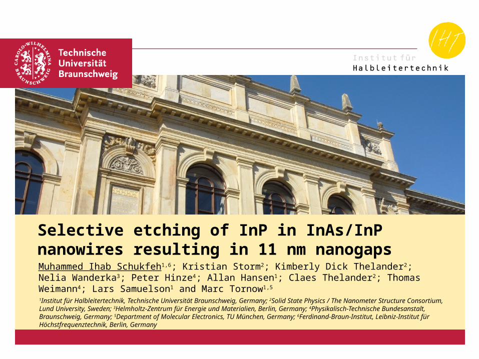
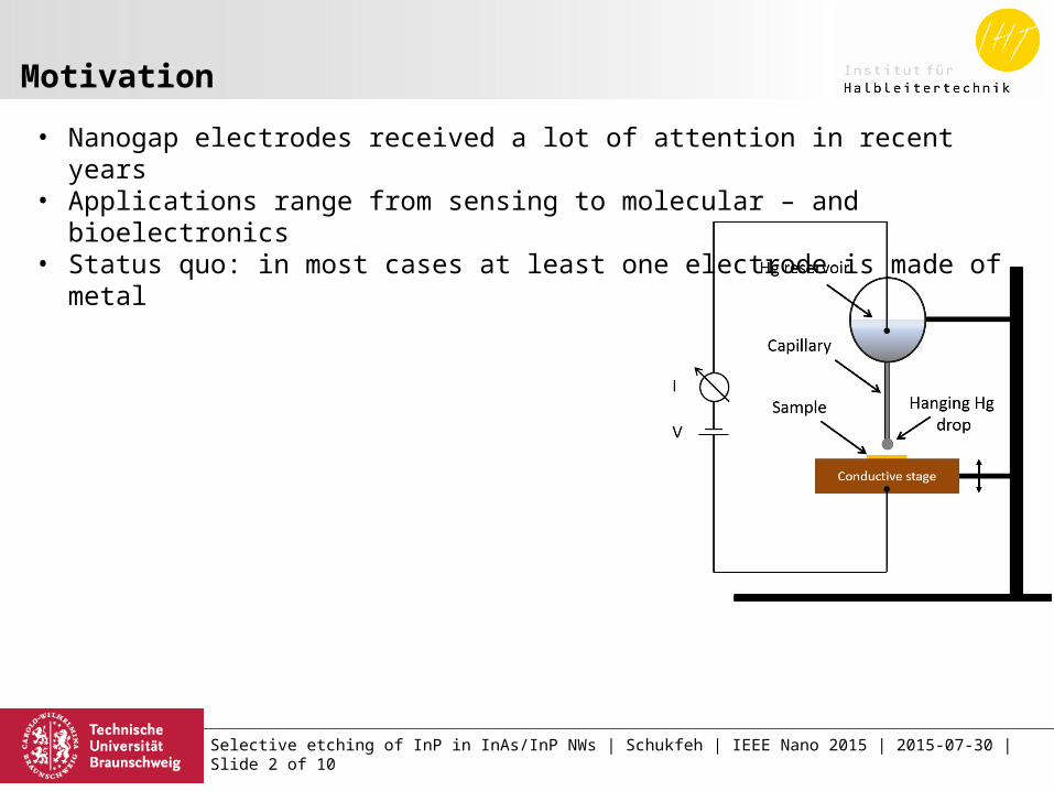
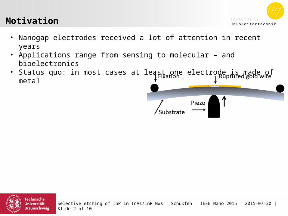
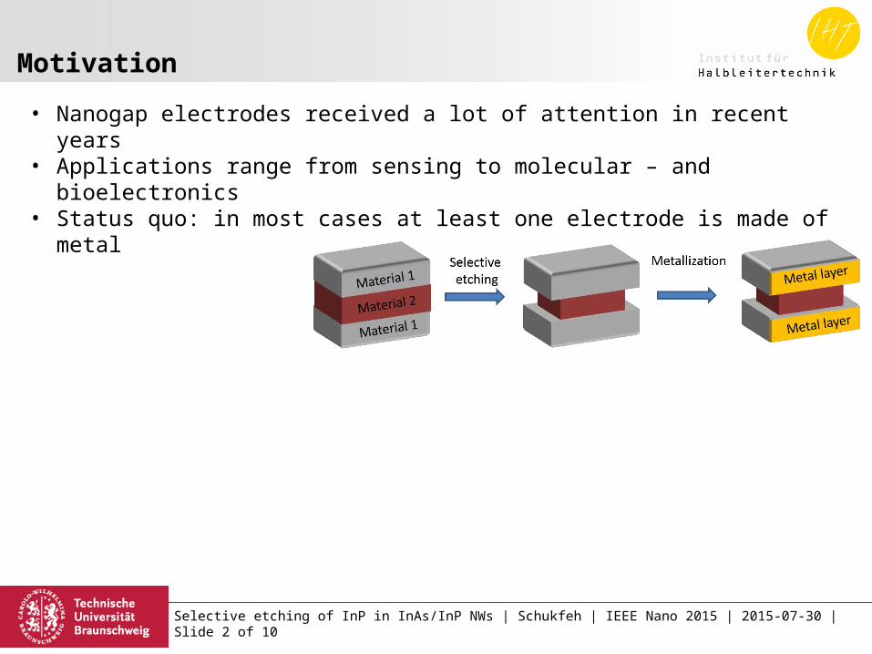
• Nanogap electrodes received a lot of attention in recent years• Applications range from sensing to molecular – and bioelectronics• Status quo: in most cases at least one electrode is made of metal
Selective etching of InP in InAs/InP NWs | Schukfeh | IEEE Nano 2015 | 2015-07-30 | Slide 2 of 10
Motivation
• Nanogap electrodes received a lot of attention in recent years• Applications range from sensing to molecular – and bioelectronics• Status quo: in most cases at least one electrode is made of metal
Advantages of semiconducting electrodes:• Tailoring physical and electrical properties according to desired application:
• Doping type
Selective etching of InP in InAs/InP NWs | Schukfeh | IEEE Nano 2015 | 2015-07-30 | Slide 2 of 10
Motivation
• Nanogap electrodes received a lot of attention in recent years• Applications range from sensing to molecular – and bioelectronics• Status quo: in most cases at least one electrode is made of metal
Advantages of semiconducting electrodes:• Tailoring physical and electrical properties according to desired application:
• Doping type• Doping concentration
Selective etching of InP in InAs/InP NWs | Schukfeh | IEEE Nano 2015 | 2015-07-30 | Slide 2 of 10
Motivation
• Nanogap electrodes received a lot of attention in recent years• Applications range from sensing to molecular – and bioelectronics• Status quo: in most cases at least one electrode is made of metal
Advantages of semiconducting electrodes:• Tailoring physical and electrical properties according to desired application:
• Doping type• Doping concentration• Band gap
Selective etching of InP in InAs/InP NWs | Schukfeh | IEEE Nano 2015 | 2015-07-30 | Slide 2 of 10

Motivation
• Nanogap electrodes received a lot of attention in recent years• Applications range from sensing to molecular – and bioelectronics• Status quo: in most cases at least one electrode is made of metal
Advantages of semiconducting electrodes:• Tailoring physical and electrical properties according to desired application:
• Doping type• Doping concentration• Band gap• Availability of native oxide
Selective etching of InP in InAs/InP NWs | Schukfeh | IEEE Nano 2015 | 2015-07-30 | Slide 2 of 10
Motivation
• Nanogap electrodes received a lot of attention in recent years• Applications range from sensing to molecular – and bioelectronics• Status quo: in most cases at least one electrode is made of metal
Advantages of semiconducting electrodes:• Tailoring physical and electrical properties according to desired application:
• Doping type• Doping concentration• Band gap• Availability of native oxide
Challenges for semiconducting nanogap electrodes:
Selective etching of InP in InAs/InP NWs | Schukfeh | IEEE Nano 2015 | 2015-07-30 | Slide 2 of 10
Motivation
• Nanogap electrodes received a lot of attention in recent years• Applications range from sensing to molecular – and bioelectronics• Status quo: in most cases at least one electrode is made of metal
Advantages of semiconducting electrodes:• Tailoring physical and electrical properties according to desired application:
• Doping type• Doping concentration• Band gap• Availability of native oxide
Challenges for semiconducting nanogap electrodes:• Technologically more demanding than metal nanogaps
Selective etching of InP in InAs/InP NWs | Schukfeh | IEEE Nano 2015 | 2015-07-30 | Slide 2 of 10
Motivation
• Nanogap electrodes received a lot of attention in recent years• Applications range from sensing to molecular – and bioelectronics• Status quo: in most cases at least one electrode is made of metal
Advantages of semiconducting electrodes:• Tailoring physical and electrical properties according to desired application:
• Doping type• Doping concentration• Band gap• Availability of native oxide
Challenges for semiconducting nanogap electrodes:• Technologically more demanding than metal nanogaps• Implementation of a gate
Selective etching of InP in InAs/InP NWs | Schukfeh | IEEE Nano 2015 | 2015-07-30 | Slide 2 of 10
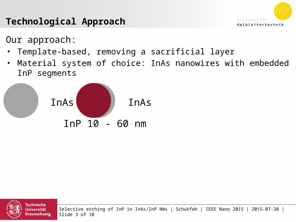
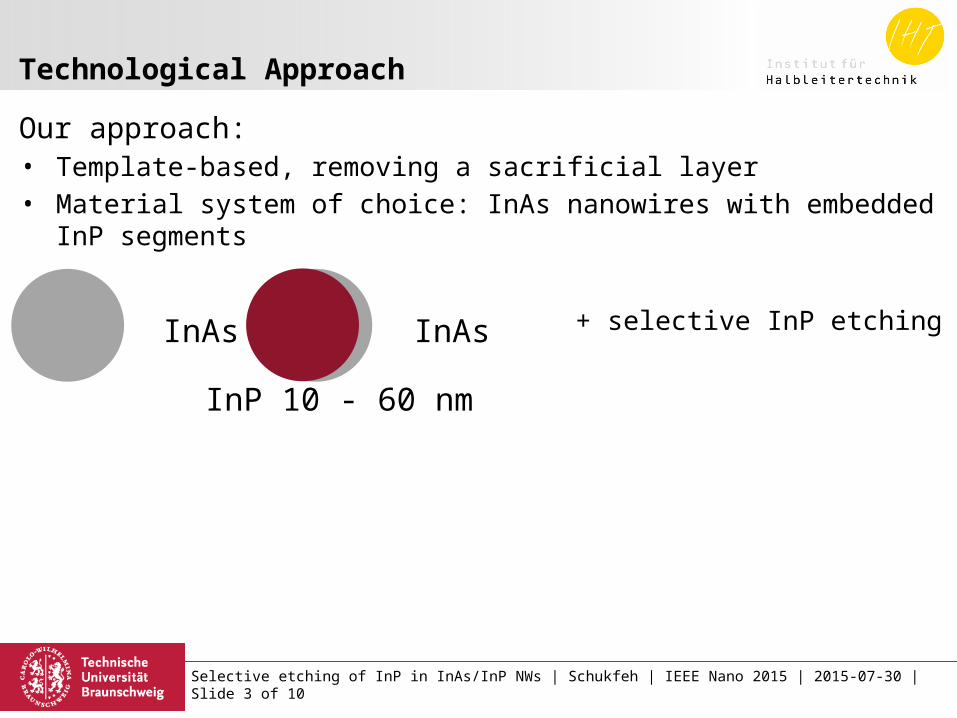
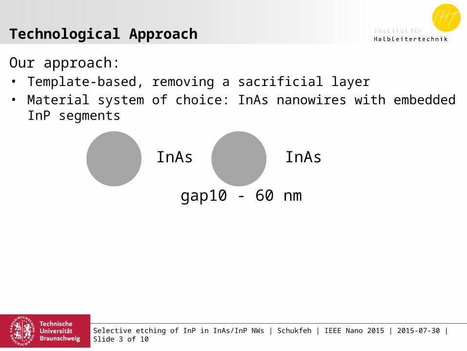
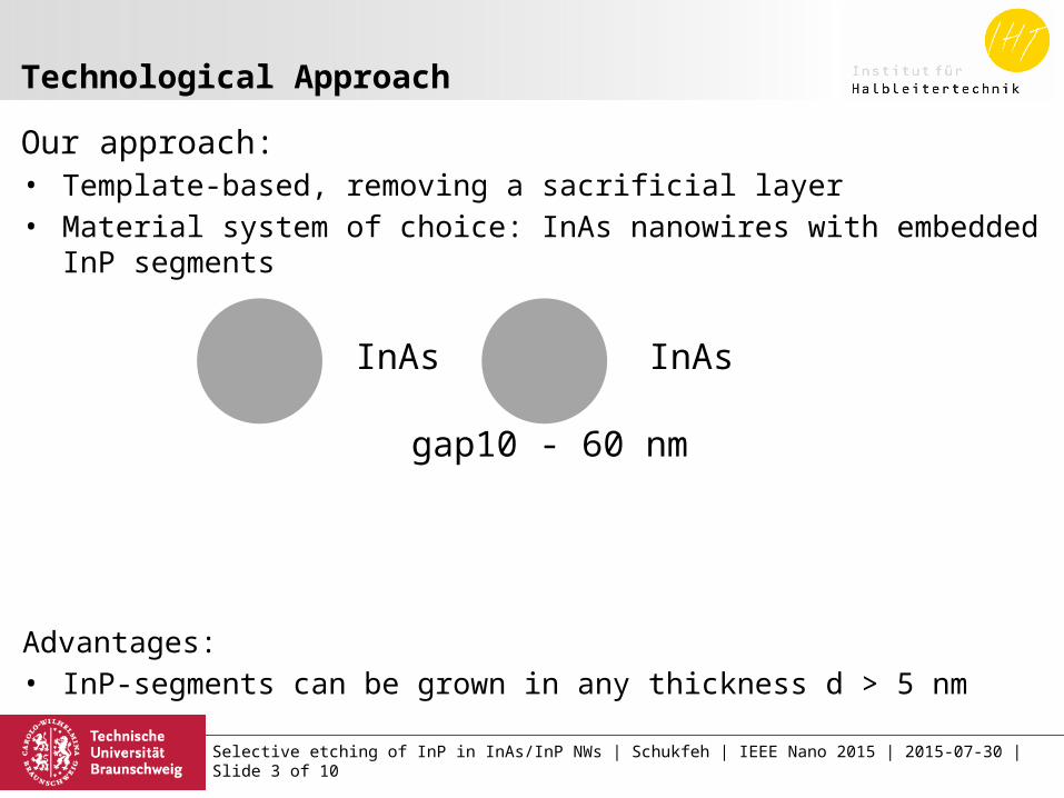
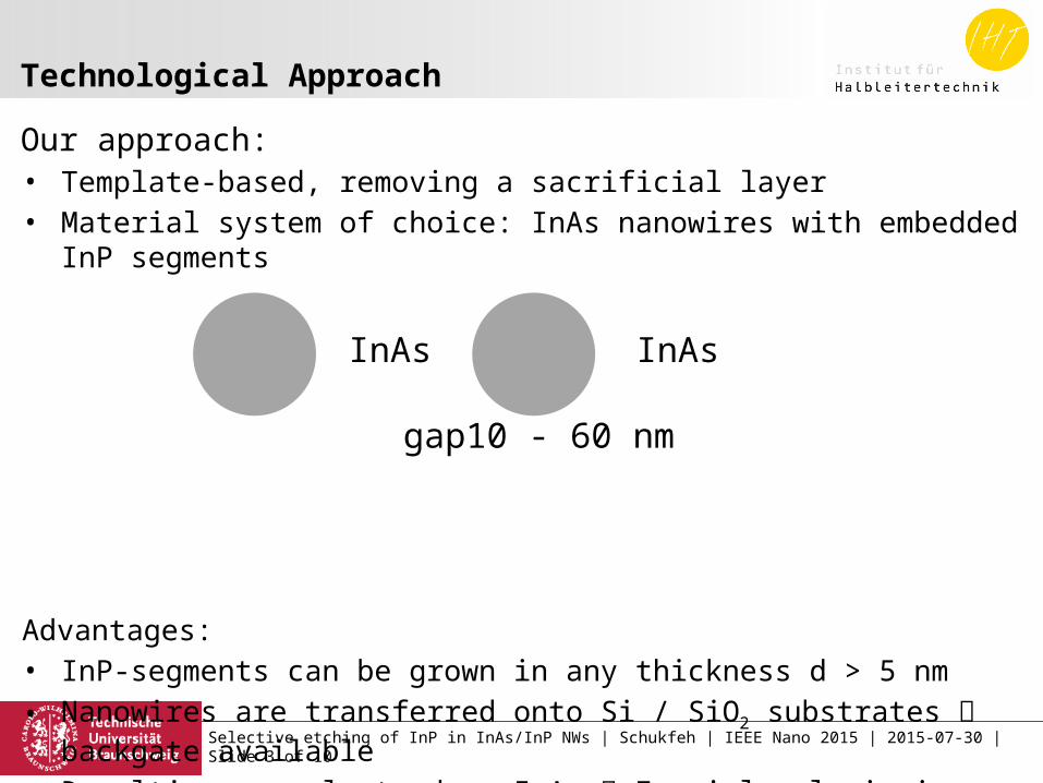
Our approach:• Template-based, removing a sacrificial layer
Technological Approach
Selective etching of InP in InAs/InP NWs | Schukfeh | IEEE Nano 2015 | 2015-07-30 | Slide 3 of 10
Our approach:• Template-based, removing a sacrificial layer• Material system of choice: InAs nanowires with embedded InP segments
Technological Approach
Selective etching of InP in InAs/InP NWs | Schukfeh | IEEE Nano 2015 | 2015-07-30 | Slide 3 of 10
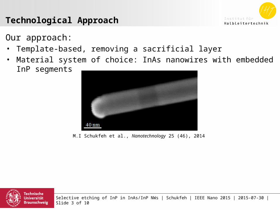
Our approach:• Template-based, removing a sacrificial layer• Material system of choice: InAs nanowires with embedded InP segments
Technological Approach
Selective etching of InP in InAs/InP NWs | Schukfeh | IEEE Nano 2015 | 2015-07-30 | Slide 3 of 10
M.I Schukfeh et al., Nanotechnology 25 (46), 2014
Our approach:• Template-based, removing a sacrificial layer• Material system of choice: InAs nanowires with embedded InP segments
Technological Approach
Selective etching of InP in InAs/InP NWs | Schukfeh | IEEE Nano 2015 | 2015-07-30 | Slide 3 of 10
InAs InAs
InP 10 - 60 nm
Our approach:• Template-based, removing a sacrificial layer• Material system of choice: InAs nanowires with embedded InP segments
Technological Approach
Selective etching of InP in InAs/InP NWs | Schukfeh | IEEE Nano 2015 | 2015-07-30 | Slide 3 of 10
InAs InAs
InP 10 - 60 nm
+ selective InP etching
Our approach:• Template-based, removing a sacrificial layer• Material system of choice: InAs nanowires with embedded InP segments
Technological Approach
Selective etching of InP in InAs/InP NWs | Schukfeh | IEEE Nano 2015 | 2015-07-30 | Slide 3 of 10
InAsInAs
gap10 - 60 nm
Our approach:• Template-based, removing a sacrificial layer• Material system of choice: InAs nanowires with embedded InP segments
Advantages:• InP-segments can be grown in any thickness d > 5 nm
Technological Approach
Selective etching of InP in InAs/InP NWs | Schukfeh | IEEE Nano 2015 | 2015-07-30 | Slide 3 of 10
InAsInAs
gap10 - 60 nm

Our approach:• Template-based, removing a sacrificial layer• Material system of choice: InAs nanowires with embedded InP segments
Advantages:• InP-segments can be grown in any thickness d > 5 nm
• Nanowires are transferred onto Si / SiO2 substrates backgate available
Technological Approach
Selective etching of InP in InAs/InP NWs | Schukfeh | IEEE Nano 2015 | 2015-07-30 | Slide 3 of 10
InAsInAs
gap10 - 60 nm
Our approach:• Template-based, removing a sacrificial layer• Material system of choice: InAs nanowires with embedded InP segments
Advantages:• InP-segments can be grown in any thickness d > 5 nm
• Nanowires are transferred onto Si / SiO2 substrates backgate available
• Resulting nanoelectrodes: InAs Fermi level pinning above conduction band edge at surface
Technological Approach
Selective etching of InP in InAs/InP NWs | Schukfeh | IEEE Nano 2015 | 2015-07-30 | Slide 3 of 10
InAsInAs
gap10 - 60 nm
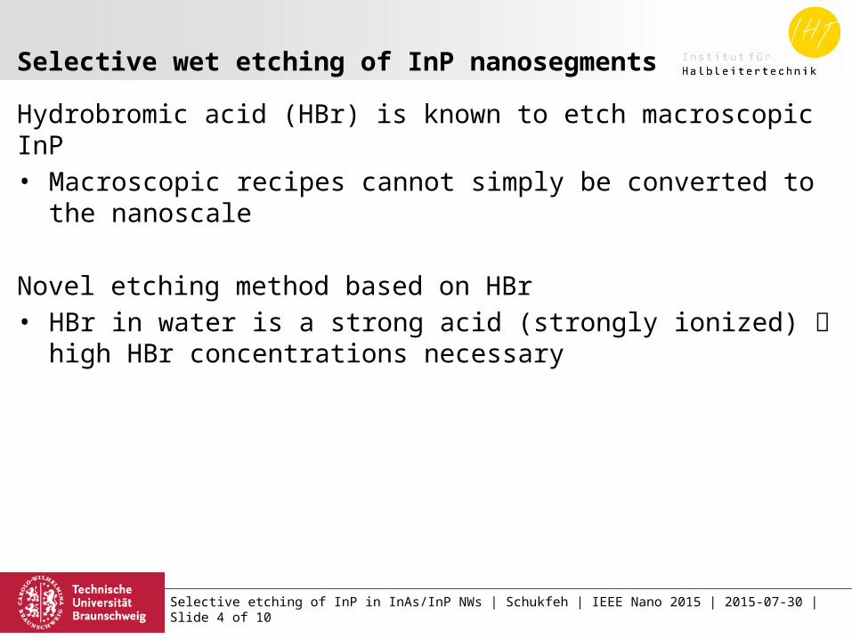
Hydrobromic acid (HBr) is known to etch macroscopic InP
Selective wet etching of InP nanosegments
Selective etching of InP in InAs/InP NWs | Schukfeh | IEEE Nano 2015 | 2015-07-30 | Slide 4 of 10
Hydrobromic acid (HBr) is known to etch macroscopic InP• Macroscopic recipes cannot simply be converted to the nanoscale
Selective wet etching of InP nanosegments
Selective etching of InP in InAs/InP NWs | Schukfeh | IEEE Nano 2015 | 2015-07-30 | Slide 4 of 10
Hydrobromic acid (HBr) is known to etch macroscopic InP• Macroscopic recipes cannot simply be converted to the nanoscale
Novel etching method based on HBr
Selective wet etching of InP nanosegments
Selective etching of InP in InAs/InP NWs | Schukfeh | IEEE Nano 2015 | 2015-07-30 | Slide 4 of 10
Hydrobromic acid (HBr) is known to etch macroscopic InP• Macroscopic recipes cannot simply be converted to the nanoscale
Novel etching method based on HBr• HBr in water is a strong acid (strongly ionized) high HBr
concentrations necessary
Selective wet etching of InP nanosegments
Selective etching of InP in InAs/InP NWs | Schukfeh | IEEE Nano 2015 | 2015-07-30 | Slide 4 of 10
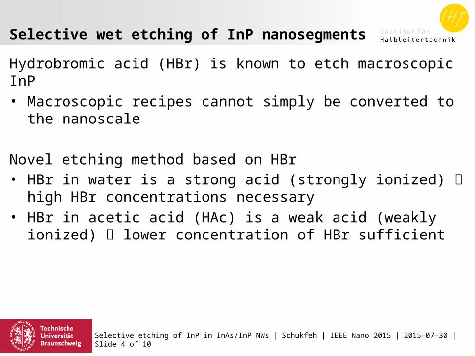
Hydrobromic acid (HBr) is known to etch macroscopic InP• Macroscopic recipes cannot simply be converted to the nanoscale
Novel etching method based on HBr• HBr in water is a strong acid (strongly ionized) high HBr
concentrations necessary• HBr in acetic acid (HAc) is a weak acid (weakly ionized) lower
concentration of HBr sufficient
Selective wet etching of InP nanosegments
Selective etching of InP in InAs/InP NWs | Schukfeh | IEEE Nano 2015 | 2015-07-30 | Slide 4 of 10
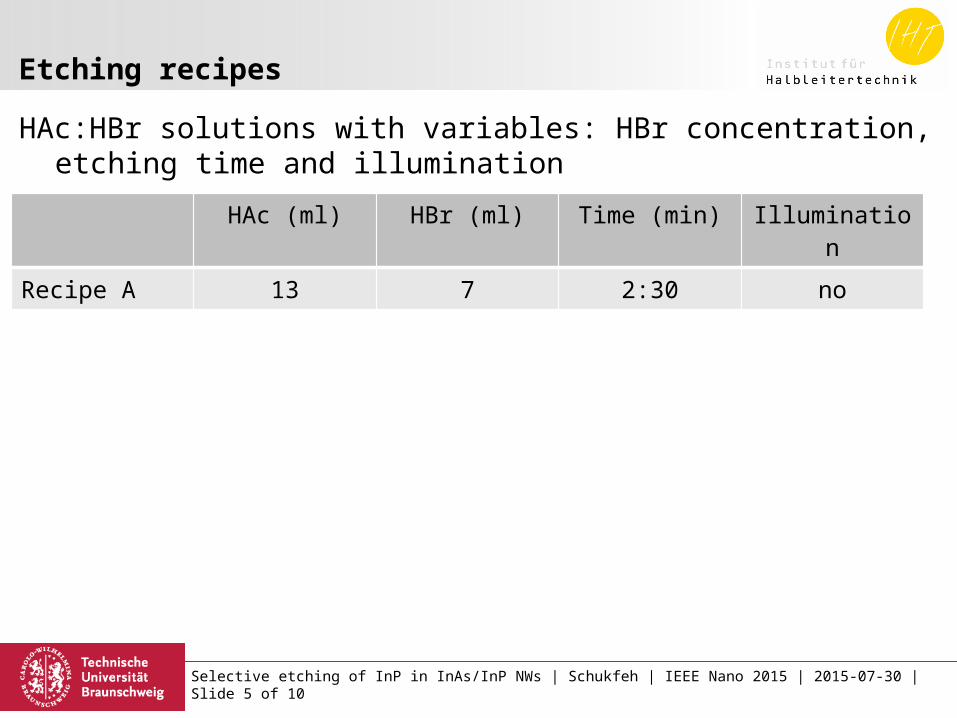
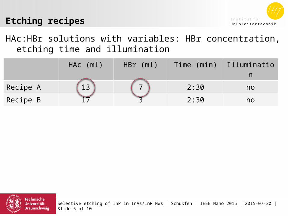
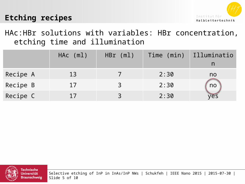
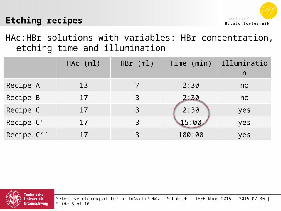
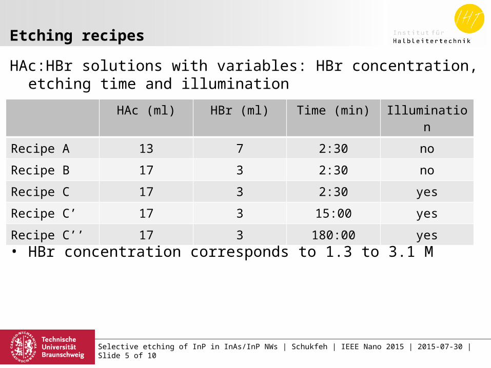
HAc:HBr solutions with variables: HBr concentration, etching time and illumination
Etching recipes
Selective etching of InP in InAs/InP NWs | Schukfeh | IEEE Nano 2015 | 2015-07-30 | Slide 5 of 10
HAc:HBr solutions with variables: HBr concentration, etching time and illumination
Etching recipes
Selective etching of InP in InAs/InP NWs | Schukfeh | IEEE Nano 2015 | 2015-07-30 | Slide 5 of 10
HAc (ml) HBr (ml) Time (min) Illumination
Recipe A 13 7 2:30 no
HAc:HBr solutions with variables: HBr concentration, etching time and illumination
Etching recipes
Selective etching of InP in InAs/InP NWs | Schukfeh | IEEE Nano 2015 | 2015-07-30 | Slide 5 of 10
HAc (ml) HBr (ml) Time (min) Illumination
Recipe A 13 7 2:30 no
Recipe B 17 3 2:30 no
HAc:HBr solutions with variables: HBr concentration, etching time and illumination
Etching recipes
Selective etching of InP in InAs/InP NWs | Schukfeh | IEEE Nano 2015 | 2015-07-30 | Slide 5 of 10
HAc (ml) HBr (ml) Time (min) Illumination
Recipe A 13 7 2:30 no
Recipe B 17 3 2:30 no
Recipe C 17 3 2:30 yes
Recipe C’ 17 3 15:00 yes
Recipe C’’ 17 3 180:00 yes
HAc:HBr solutions with variables: HBr concentration, etching time and illumination
• HBr concentration corresponds to 1.3 to 3.1 M
Etching recipes
Selective etching of InP in InAs/InP NWs | Schukfeh | IEEE Nano 2015 | 2015-07-30 | Slide 5 of 10
HAc (ml) HBr (ml) Time (min) Illumination
Recipe A 13 7 2:30 no
Recipe B 17 3 2:30 no
Recipe C 17 3 2:30 yes
Recipe C’ 17 3 15:00 yes
Recipe C’’ 17 3 180:00 yes

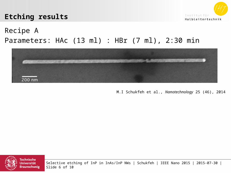
Recipe A
Parameters: HAc (13 ml) : HBr (7 ml), 2:30 min
Etching results
Selective etching of InP in InAs/InP NWs | Schukfeh | IEEE Nano 2015 | 2015-07-30 | Slide 6 of 10
Recipe A
Parameters: HAc (13 ml) : HBr (7 ml), 2:30 min
Etching results
Selective etching of InP in InAs/InP NWs | Schukfeh | IEEE Nano 2015 | 2015-07-30 | Slide 6 of 10
M.I Schukfeh et al., Nanotechnology 25 (46), 2014

Etching results
Selective etching of InP in InAs/InP NWs | Schukfeh | IEEE Nano 2015 | 2015-07-30 | Slide 6 of 10
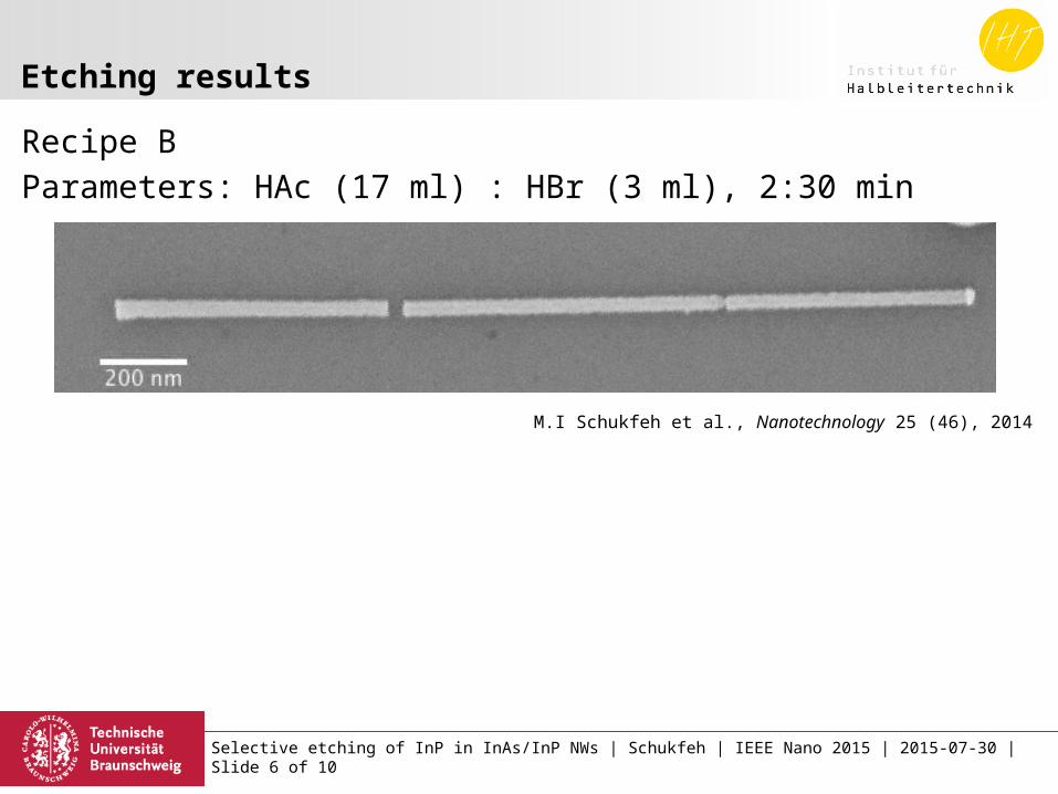
Recipe B
Parameters: HAc (17 ml) : HBr (3 ml), 2:30 min
Etching results
Selective etching of InP in InAs/InP NWs | Schukfeh | IEEE Nano 2015 | 2015-07-30 | Slide 6 of 10
Recipe B
Parameters: HAc (17 ml) : HBr (3 ml), 2:30 min
M.I Schukfeh et al., Nanotechnology 25 (46), 2014
Etching results
Selective etching of InP in InAs/InP NWs | Schukfeh | IEEE Nano 2015 | 2015-07-30 | Slide 6 of 10
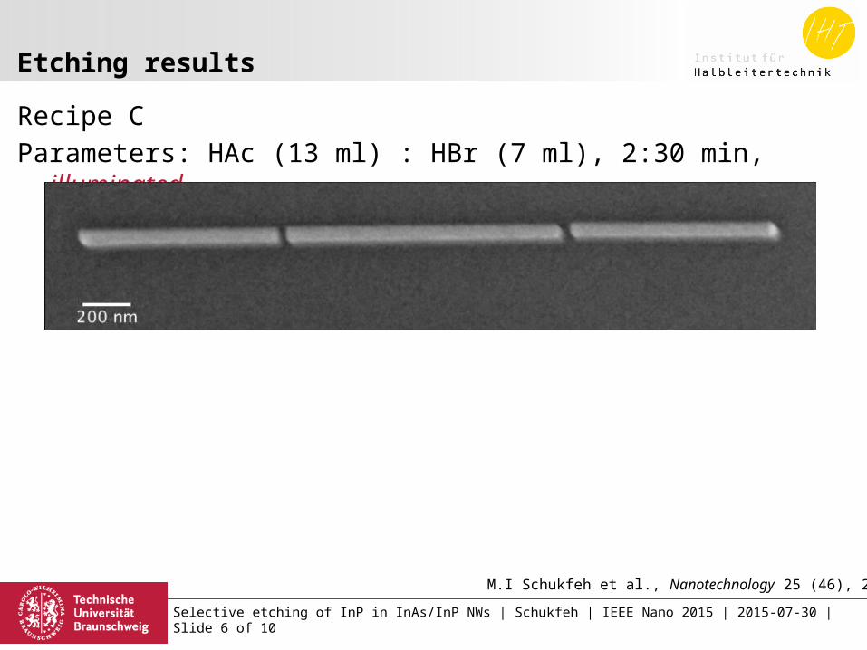
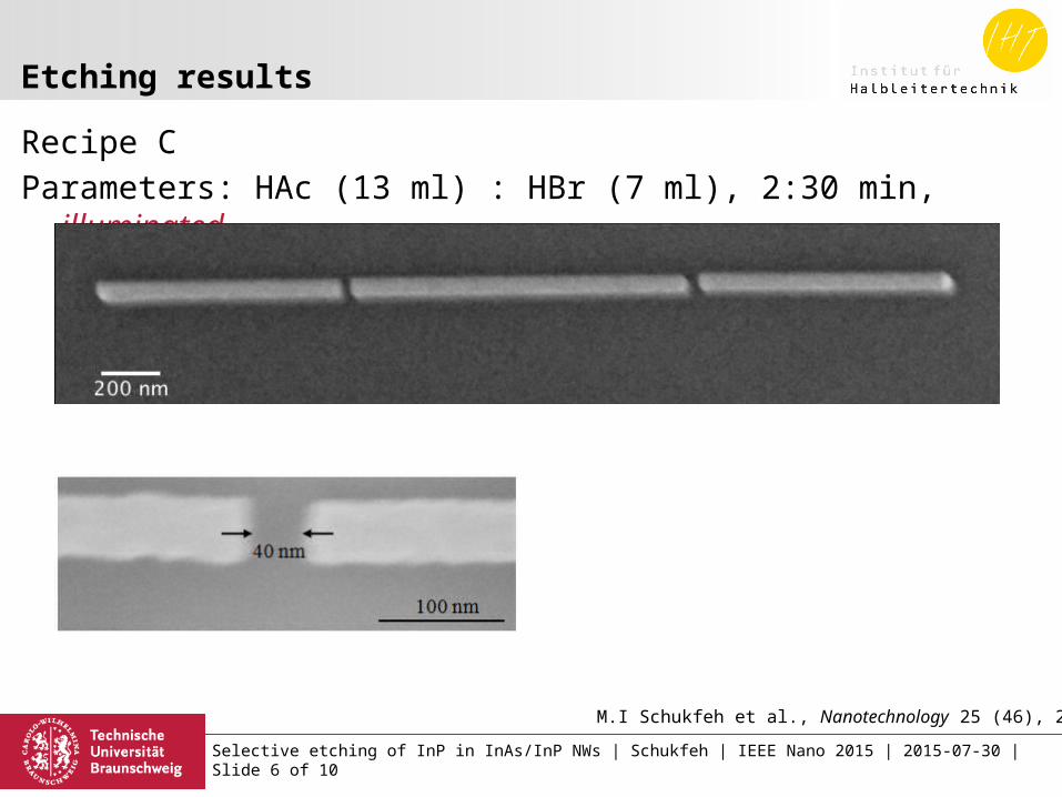
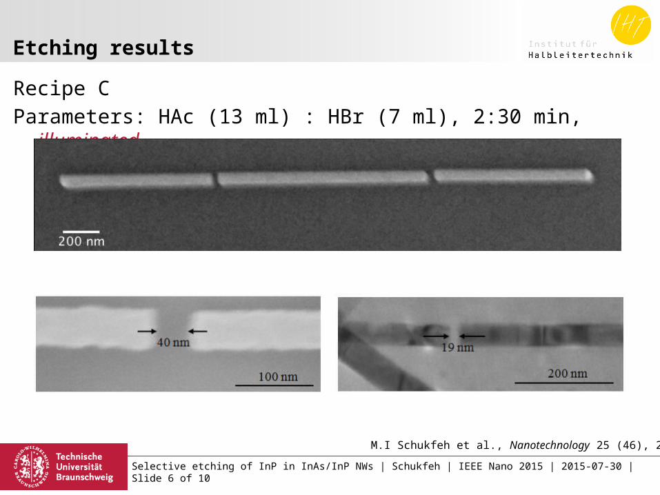
Recipe C
Parameters: HAc (13 ml) : HBr (7 ml), 2:30 min, illuminated
Etching results
Selective etching of InP in InAs/InP NWs | Schukfeh | IEEE Nano 2015 | 2015-07-30 | Slide 6 of 10
Recipe C
Parameters: HAc (13 ml) : HBr (7 ml), 2:30 min, illuminated
M.I Schukfeh et al., Nanotechnology 25 (46), 2014
Etching results
Selective etching of InP in InAs/InP NWs | Schukfeh | IEEE Nano 2015 | 2015-07-30 | Slide 6 of 10
Recipe C
Parameters: HAc (13 ml) : HBr (7 ml), 2:30 min, illuminated
M.I Schukfeh et al., Nanotechnology 25 (46), 2014
Etching results
Selective etching of InP in InAs/InP NWs | Schukfeh | IEEE Nano 2015 | 2015-07-30 | Slide 6 of 10
Recipe C
Parameters: HAc (13 ml) : HBr (7 ml), 2:30 min, illuminated
M.I Schukfeh et al., Nanotechnology 25 (46), 2014
Etching results
Selective etching of InP in InAs/InP NWs | Schukfeh | IEEE Nano 2015 | 2015-07-30 | Slide 6 of 10
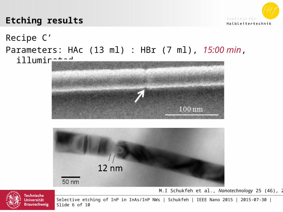
Recipe C’
Parameters: HAc (13 ml) : HBr (7 ml), 15:00 min, illuminated
Etching results
Selective etching of InP in InAs/InP NWs | Schukfeh | IEEE Nano 2015 | 2015-07-30 | Slide 6 of 10
M.I Schukfeh et al., Nanotechnology 25 (46), 2014
Recipe C’
Parameters: HAc (13 ml) : HBr (7 ml), 15:00 min, illuminated
Etching results
Selective etching of InP in InAs/InP NWs | Schukfeh | IEEE Nano 2015 | 2015-07-30 | Slide 6 of 10
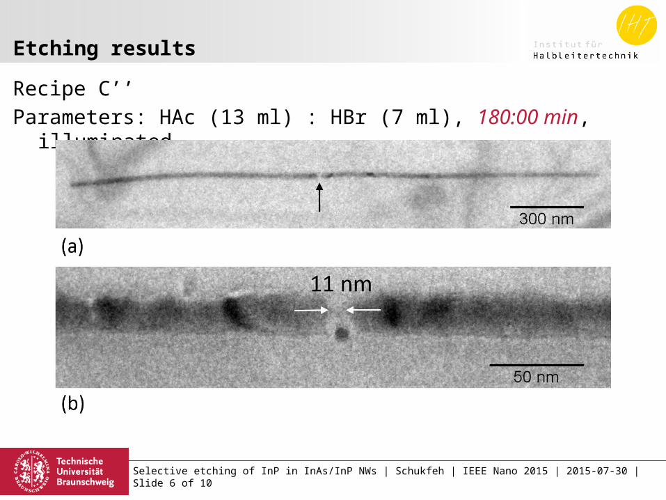
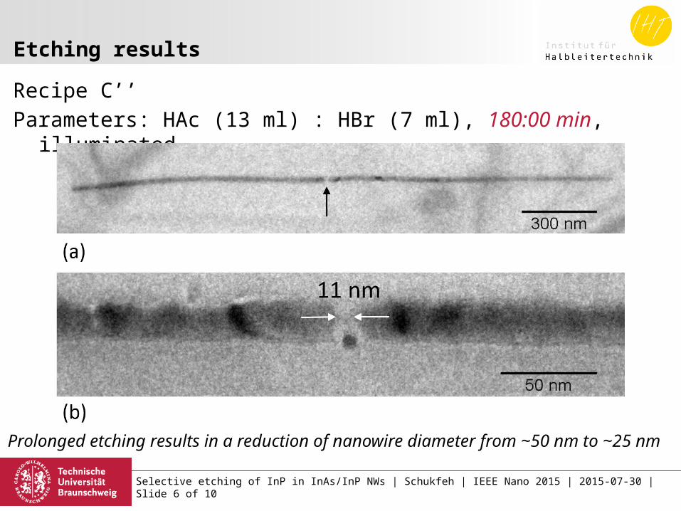
Recipe C’’
Parameters: HAc (13 ml) : HBr (7 ml), 180:00 min, illuminated
Etching results
Selective etching of InP in InAs/InP NWs | Schukfeh | IEEE Nano 2015 | 2015-07-30 | Slide 6 of 10
Recipe C’’
Parameters: HAc (13 ml) : HBr (7 ml), 180:00 min, illuminated
Etching results
Selective etching of InP in InAs/InP NWs | Schukfeh | IEEE Nano 2015 | 2015-07-30 | Slide 6 of 10
Prolonged etching results in a reduction of nanowire diameter from ~50 nm to ~25 nm
Recipe C’’
Parameters: HAc (13 ml) : HBr (7 ml), 180:00 min, illuminated
Etching of InP (InAs accordingly) with HBr proceeds in 2-step process:
Etching process
Selective etching of InP in InAs/InP NWs | Schukfeh | IEEE Nano 2015 | 2015-07-30 | Slide 7 of 10
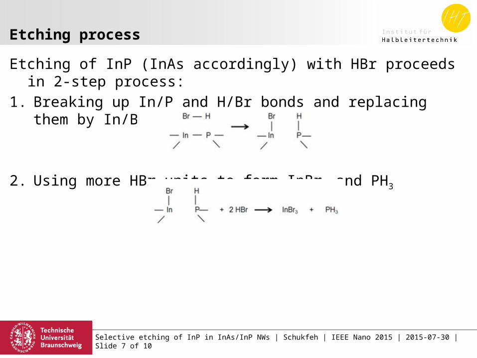
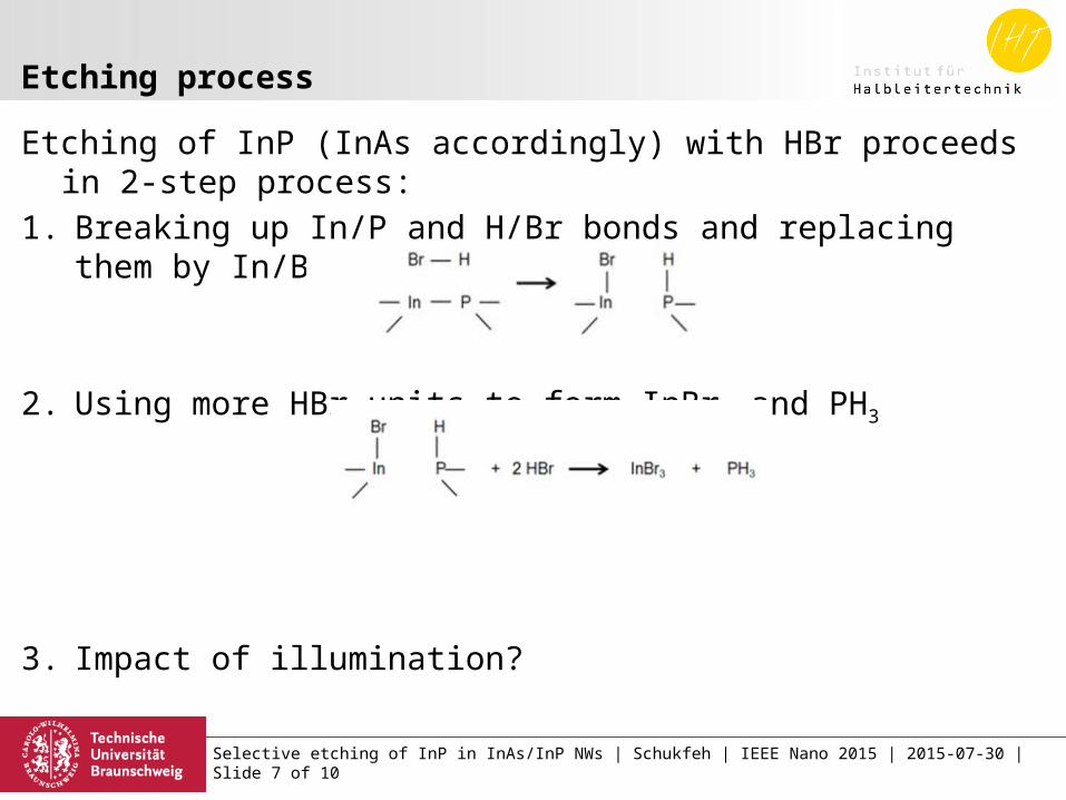
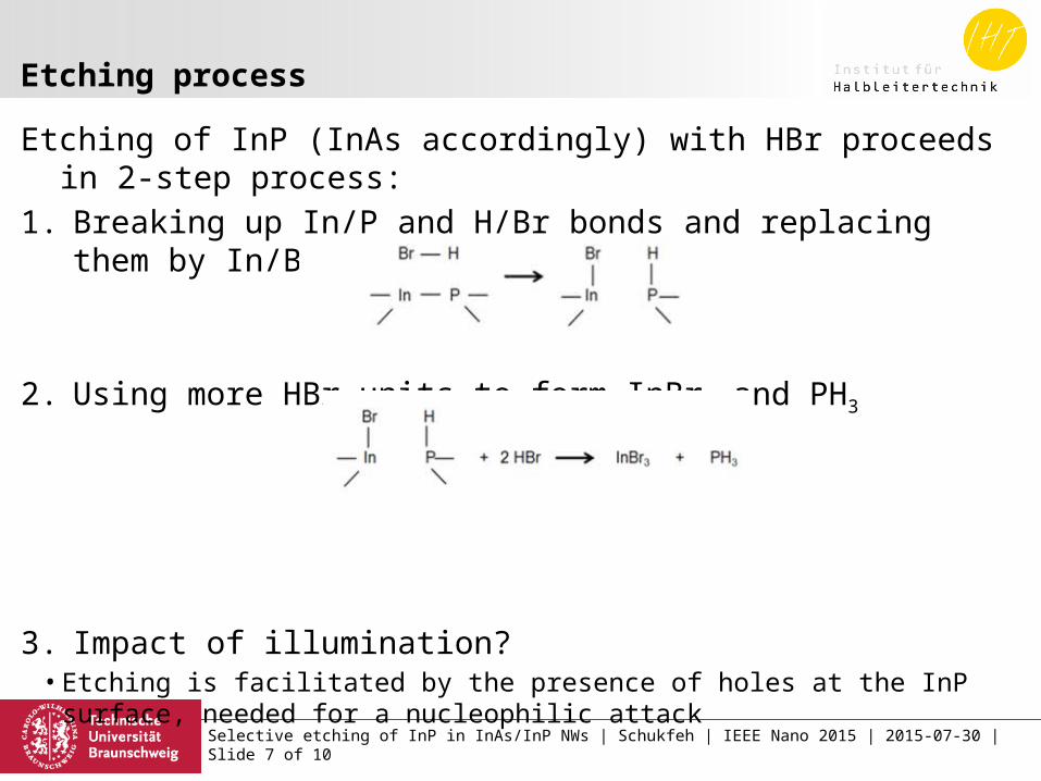
Etching of InP (InAs accordingly) with HBr proceeds in 2-step process:
1. Breaking up In/P and H/Br bonds and replacing them by In/Br and P/H bonds
Etching process
Selective etching of InP in InAs/InP NWs | Schukfeh | IEEE Nano 2015 | 2015-07-30 | Slide 7 of 10

Etching of InP (InAs accordingly) with HBr proceeds in 2-step process:
1. Breaking up In/P and H/Br bonds and replacing them by In/Br and P/H bonds
Etching process
Selective etching of InP in InAs/InP NWs | Schukfeh | IEEE Nano 2015 | 2015-07-30 | Slide 7 of 10

Etching of InP (InAs accordingly) with HBr proceeds in 2-step process:
1. Breaking up In/P and H/Br bonds and replacing them by In/Br and P/H bonds
2. Using more HBr units to form InBr3 and PH3
Etching process
Selective etching of InP in InAs/InP NWs | Schukfeh | IEEE Nano 2015 | 2015-07-30 | Slide 7 of 10
Etching of InP (InAs accordingly) with HBr proceeds in 2-step process:
1. Breaking up In/P and H/Br bonds and replacing them by In/Br and P/H bonds
2. Using more HBr units to form InBr3 and PH3
3. Impact of illumination?
Etching process
Selective etching of InP in InAs/InP NWs | Schukfeh | IEEE Nano 2015 | 2015-07-30 | Slide 7 of 10
Etching of InP (InAs accordingly) with HBr proceeds in 2-step process:
1. Breaking up In/P and H/Br bonds and replacing them by In/Br and P/H bonds
2. Using more HBr units to form InBr3 and PH3
3. Impact of illumination?• Etching is facilitated by the presence of holes at the InP surface, needed for a
nucleophilic attack
Etching process
Selective etching of InP in InAs/InP NWs | Schukfeh | IEEE Nano 2015 | 2015-07-30 | Slide 7 of 10

Etching of InP (InAs accordingly) with HBr proceeds in 2-step process:
1. Breaking up In/P and H/Br bonds and replacing them by In/Br and P/H bonds
2. Using more HBr units to form InBr3 and PH3
3. Impact of illumination?• Etching is facilitated by the presence of holes at the InP surface, needed for a
nucleophilic attack• Light generates electron / hole pairs
Etching process
Selective etching of InP in InAs/InP NWs | Schukfeh | IEEE Nano 2015 | 2015-07-30 | Slide 7 of 10
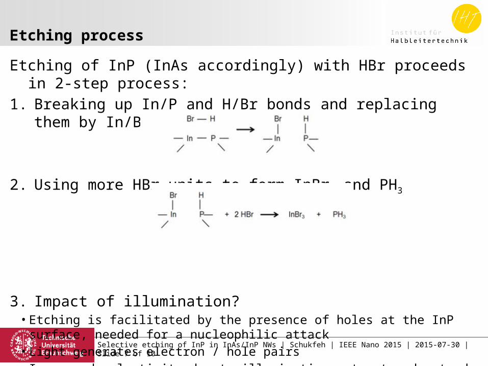
Etching of InP (InAs accordingly) with HBr proceeds in 2-step process:
1. Breaking up In/P and H/Br bonds and replacing them by In/Br and P/H bonds
2. Using more HBr units to form InBr3 and PH3
3. Impact of illumination?• Etching is facilitated by the presence of holes at the InP surface, needed for a
nucleophilic attack• Light generates electron / hole pairs• Increased selectivity due to illumination not yet understood
Etching process
Selective etching of InP in InAs/InP NWs | Schukfeh | IEEE Nano 2015 | 2015-07-30 | Slide 7 of 10
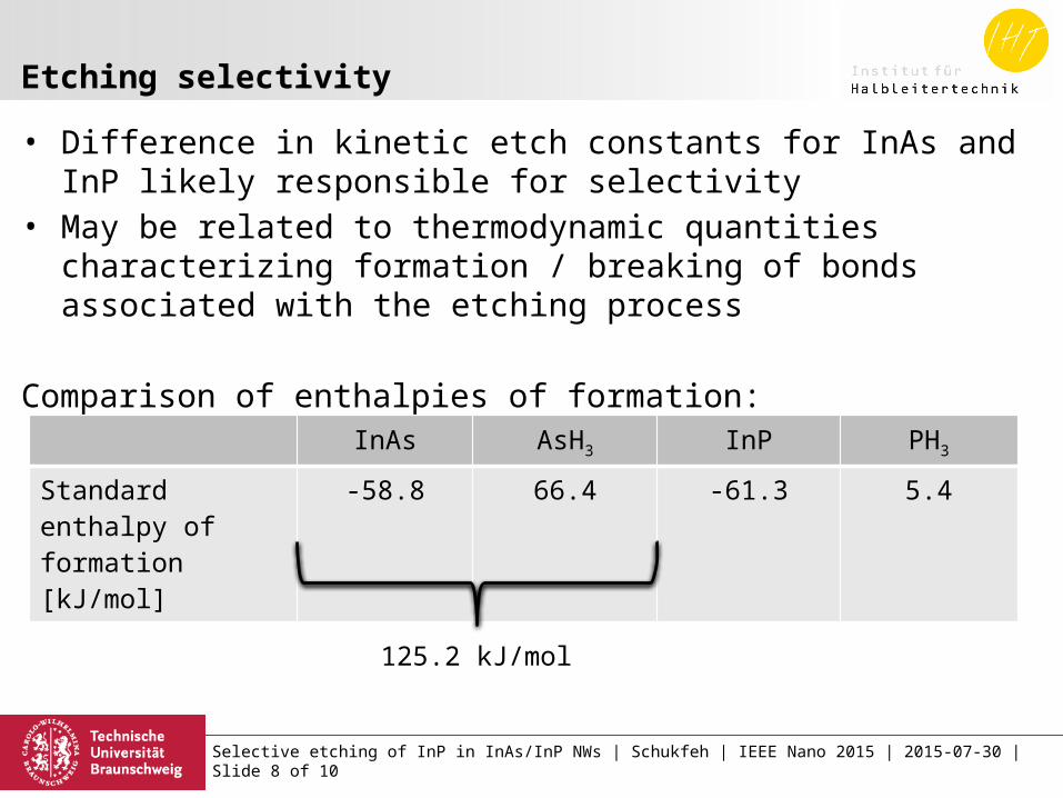
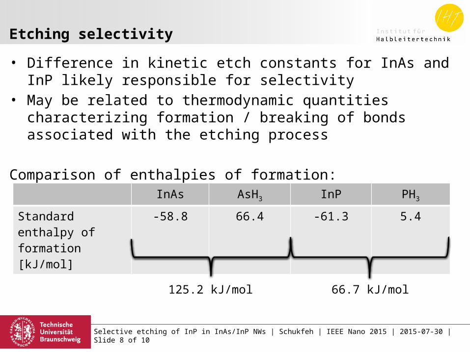
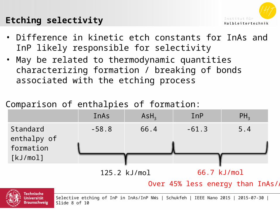
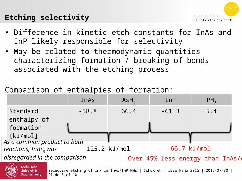
• Difference in kinetic etch constants for InAs and InP likely responsible for selectivity
Etching selectivity
Selective etching of InP in InAs/InP NWs | Schukfeh | IEEE Nano 2015 | 2015-07-30 | Slide 8 of 10
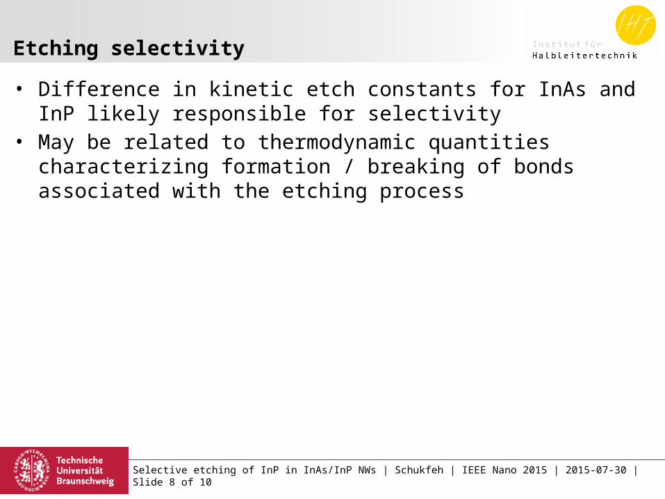
• Difference in kinetic etch constants for InAs and InP likely responsible for selectivity
• May be related to thermodynamic quantities characterizing formation / breaking of bonds associated with the etching process
Comparison of enthalpies of formation:
Etching selectivity
Selective etching of InP in InAs/InP NWs | Schukfeh | IEEE Nano 2015 | 2015-07-30 | Slide 8 of 10
InAs AsH3 InP PH3
Standard enthalpy of formation [kJ/mol]
-58.8 66.4
125.2 kJ/mol
• Difference in kinetic etch constants for InAs and InP likely responsible for selectivity
• May be related to thermodynamic quantities characterizing formation / breaking of bonds associated with the etching process
Comparison of enthalpies of formation:
Etching selectivity
Selective etching of InP in InAs/InP NWs | Schukfeh | IEEE Nano 2015 | 2015-07-30 | Slide 8 of 10
InAs AsH3 InP PH3
Standard enthalpy of formation [kJ/mol]
-58.8 66.4 -61.3 5.4
125.2 kJ/mol 66.7 kJ/mol
Over 45% less energy than InAs/AsH3
As a common product to both reactions, InBr3 was disregarded in the comparison
• A selective wet etching technique was developed to remove embedded nanoscale InP segments from InAs nanowires
Conclusion & Outlook
Selective etching of InP in InAs/InP NWs | Schukfeh | IEEE Nano 2015 | 2015-07-30 | Slide 9 of 10
• A selective wet etching technique was developed to remove embedded nanoscale InP segments from InAs nanowires
• InP segments of 10 nm thickness in 50 nm diameter nanowires were successfully removed, yielding nanometer-spaced InAs electrodes
• For prolonged etching, InAs nanowire diameter was reduced from 50 to 25 nm
Conclusion & Outlook
Selective etching of InP in InAs/InP NWs | Schukfeh | IEEE Nano 2015 | 2015-07-30 | Slide 9 of 10

• A selective wet etching technique was developed to remove embedded nanoscale InP segments from InAs nanowires
• InP segments of 10 nm thickness in 50 nm diameter nanowires were successfully removed, yielding nanometer-spaced InAs electrodes
• For prolonged etching, InAs nanowire diameter was reduced from 50 to 25 nm
Future work:
Conclusion & Outlook
Selective etching of InP in InAs/InP NWs | Schukfeh | IEEE Nano 2015 | 2015-07-30 | Slide 9 of 10
• A selective wet etching technique was developed to remove embedded nanoscale InP segments from InAs nanowires
• InP segments of 10 nm thickness in 50 nm diameter nanowires were successfully removed, yielding nanometer-spaced InAs electrodes
• For prolonged etching, InAs nanowire diameter was reduced from 50 to 25 nm
Future work:• Pushing towards removal of smaller (~5 nm) InP segments
Conclusion & Outlook
Selective etching of InP in InAs/InP NWs | Schukfeh | IEEE Nano 2015 | 2015-07-30 | Slide 9 of 10
• A selective wet etching technique was developed to remove embedded nanoscale InP segments from InAs nanowires
• InP segments of 10 nm thickness in 50 nm diameter nanowires were successfully removed, yielding nanometer-spaced InAs electrodes
• For prolonged etching, InAs nanowire diameter was reduced from 50 to 25 nm
Future work:• Pushing towards removal of smaller (~5 nm) InP segments• Application in molecular electronics circuits
Conclusion & Outlook
Selective etching of InP in InAs/InP NWs | Schukfeh | IEEE Nano 2015 | 2015-07-30 | Slide 9 of 10
• A selective wet etching technique was developed to remove embedded nanoscale InP segments from InAs nanowires
• InP segments of 10 nm thickness in 50 nm diameter nanowires were successfully removed, yielding nanometer-spaced InAs electrodes
• For prolonged etching, InAs nanowire diameter was reduced from 50 to 25 nm
Future work:• Pushing towards removal of smaller (~5 nm) InP segments• Application in molecular electronics circuits• Understanding role of illumination for enhanced selectivity
(InP/InAs)
Conclusion & Outlook
Selective etching of InP in InAs/InP NWs | Schukfeh | IEEE Nano 2015 | 2015-07-30 | Slide 9 of 10
…for your attention.
Acknowledgments
Meinhard Schilling, EMG, TU Braunschweig, Germany
Frank Ludwig, EMG, TU Braunschweig, Germany
Partially funded by
Thank you…
Selective etching of InP in InAs/InP NWs | Schukfeh | IEEE Nano 2015 | 2015-07-30 | Slide 10 of 10