Embed Size (px)
Citation preview

Instructions for use
Title Induced charge density wave and superconductivity in Cu-doped TaSe₃
Author(s) 野村, 温
Citation 北海道大学. 博士(工学) 甲第13634号
Issue Date 2019-03-25
DOI 10.14943/doctoral.k13634
Doc URL http://hdl.handle.net/2115/74056
Type theses (doctoral)
File Information Atsushi_Nomura.pdf
Hokkaido University Collection of Scholarly and Academic Papers : HUSCAP
Doctoral thesis
Induced charge density wave andsuperconductivity in Cu-doped TaSe3
Atsushi Nomura
Department of Applied Physics,Hokkaido University
March 2019
Abstract
The relationship between superconductivity (SC) and charge density wave (CDW) has
been a major research topic in condensed matter physics and has been investigated in
many materials. However, previous studies were actually limited to two cases: the first
is where SC and a CDW intrinsically exist; the second is where SC is induced in a CDW
material. To understand the whole picture of the relationship between SC and CDW, we
investigated the relationship in a third case where a CDW is induced in a superconducting
material.
Transition metal trichalcogenides, MX3 (M: Nb, Ta; X: S, Se), has a structure consisting
of chains made of transition metals and chalcogens, and the chains are weakly bonded by
van der Waals forces. Owing to this structure, MX3 is a quasi-one-dimensional conductor
in which an electric current travels well in the direction of the chain axis. In most
materials belonging to MX3 (NbSe3, TaS3, and NbS3), the Fermi surface is close to a
plane. Therefore, the nesting condition is good and a CDW develops below the transition
temperature in these materials. On the other hand, TaSe3 which is one of MX3 exhibits
no CDW transition but the filamentary superconductivity transition at about 2 K because
TaSe3 is more three-dimensional than the other MX3 compounds.
If Cu atoms are doped in TaSe3, the Cu atoms are considered to be difficult to substitute
for Ta atoms because the common valence that Cu takes (+1 or +2) is different from that
of Ta (+5). On the other hand, the Cu atoms are expected to enter in the Van der Waals
gap and to increase the distance between chains of TaSe3. Therefore, it is presumed that
Cu doping decreases the dimensionality and improves the nesting condition in TaSe3.
In this thesis, we tried to induce a CDW in TaSe3 with a superconducting material by
Cu doping, and investigated the relationship between the induced CDW and SC.
We have synthesized single crystals of Cu-doped TaSe3, and measured precisely the
temperature dependence of the resistance from 4.2 to 280 K. We discover an anomalous
sharp dip in the temperature derivative of the resistance (dR/dT ) at about 91 K in Cu-
doped TaSe3, which is never observed in pure TaSe3. The dip suggests that there is a
1
sudden change in state with a relative increase in resistance. In addition, the dip is “γ”
shaped. We reveal that the same “γ”-shaped dip in dR/dT is commonly observed at the
CDW transition temperature in many CDW conductors, which is a universal consequence
resulting from the opening and growth of a CDW gap on a Fermi surface. Furthermore,
the result of the single-crystal X-ray diffraction (XRD) analysis implies that the lattice pa-
rameters perpendicular the chain axis increase and that parallel to the chain axis decreases
by Cu doping, leading to an improvement in the nesting condition. The “γ”-shaped dip
and the result of the single-crystal XRD analysis show that a CDW emerges by Cu doping
in TaSe3.
We investigated the effect of Cu doping on SC in Cu-doped TaSe3 by measuring the
temperature dependence of the resistance from 0.6 to 2 K. We observed an emergence of
a region where the SC transition temperature (TC) decreased in samples with higher Cu
concentrations, and found that the region tended to expand with increasing Cu concen-
tration. These results and the fact that the SC of TaSe3 is filamentary show that SC is
suppressed locally by Cu doping in Cu-doped TaSe3.
From the above discussions, it was revealed that a CDW is induced while SC is sup-
pressed in Cu-doped TaSe3. Hence, the induced CDW and SC would be in a competitive
relationship.
The locality of SC suppression suggests that the induced CDWs are local. The resis-
tance anomaly due to the induced CDW transition was extremely small. Moreover, the
size of the anomaly was enhanced with increasing Cu concentration but the temperature
at which the anomaly appeared hardly changed. These results of the anomaly can be
interpreted consistently from the short-range order of the induced CDWs in the vicinity
of Cu atoms.
From all the discussions, we conclude that the induced short-range order CDWs and
SC are in a competitive relationship in Cu-doped TaSe3. The competitive relationship
between short-range order CDWs and SC obtained in the present work is different from
the non-competitive relationship previously reported in CuxTiSe2 where SC is induced in
a CDW material. By comparing the detailed experimental results of these two materials,
we will clarify the physics that defines the relationship between short-range order CDWs
and SC.
2
Contents
Outline of this thesis 5
1 General introduction 6
1.1 Induction of macroscopic quantum state . . . . . . . . . . . . . . . . . . . 6
1.2 Relationship between charge density wave (CDW) and superconductivity . 8
1.3 Purpose of this study . . . . . . . . . . . . . . . . . . . . . . . . . . . . . . 13
2 Emergence of a CDW in Cu-doped TaSe3 14
2.1 Introduction . . . . . . . . . . . . . . . . . . . . . . . . . . . . . . . . . . . 14
2.1.1 TaSe3 . . . . . . . . . . . . . . . . . . . . . . . . . . . . . . . . . . 14
2.1.2 Cu doping . . . . . . . . . . . . . . . . . . . . . . . . . . . . . . . . 18
2.1.3 Purpose of this study . . . . . . . . . . . . . . . . . . . . . . . . . . 18
2.2 Experimental . . . . . . . . . . . . . . . . . . . . . . . . . . . . . . . . . . 19
2.2.1 Synthesis of single crystals . . . . . . . . . . . . . . . . . . . . . . . 19
2.2.2 Inductively coupled plasma atomic emission spectroscopy . . . . . . 20
2.2.3 Single-crystal X-ray diffraction (XRD) . . . . . . . . . . . . . . . . 20
2.2.4 Resistance measurement . . . . . . . . . . . . . . . . . . . . . . . . 21
2.3 Results . . . . . . . . . . . . . . . . . . . . . . . . . . . . . . . . . . . . . . 22
2.3.1 Crystal . . . . . . . . . . . . . . . . . . . . . . . . . . . . . . . . . . 22
2.3.2 Result of single-crystal XRD . . . . . . . . . . . . . . . . . . . . . . 24
2.3.3 Resistance measurement results from 4.2 K to 280 K . . . . . . . . 26
2.4 Discussion . . . . . . . . . . . . . . . . . . . . . . . . . . . . . . . . . . . . 29
2.4.1 Change in the lattice parameters by Cu doping . . . . . . . . . . . 29
2.4.2 Change in the number of carriers by Cu doping . . . . . . . . . . . 30
2.4.3 “γ”-shaped dip . . . . . . . . . . . . . . . . . . . . . . . . . . . . . 30
2.4.4 Emergence of a CDW . . . . . . . . . . . . . . . . . . . . . . . . . . 35
2.4.5 The CDW formation in the saddle-point mechanism . . . . . . . . . 35
3
2.5 Conclusion . . . . . . . . . . . . . . . . . . . . . . . . . . . . . . . . . . . . 36
3 Superconductivity in Cu-doped TaSe3 37
3.1 Introduction . . . . . . . . . . . . . . . . . . . . . . . . . . . . . . . . . . . 37
3.2 Experimental . . . . . . . . . . . . . . . . . . . . . . . . . . . . . . . . . . 39
3.2.1 Synthesis of single crystals . . . . . . . . . . . . . . . . . . . . . . . 39
3.2.2 Resistance measurement . . . . . . . . . . . . . . . . . . . . . . . . 39
3.3 Results . . . . . . . . . . . . . . . . . . . . . . . . . . . . . . . . . . . . . . 41
3.3.1 Resistance measurement results from 2 K to 280 K . . . . . . . . . 41
3.3.2 Resistance measurement results from 0.6 K to 2 K . . . . . . . . . . 44
3.3.3 The location dependence of the superconductivity transition . . . . 46
3.3.4 The superconductivity transition under static magnetic fields . . . . 48
3.4 Discussion . . . . . . . . . . . . . . . . . . . . . . . . . . . . . . . . . . . . 50
3.4.1 Model of the superconducting filament structure . . . . . . . . . . . 50
3.4.2 Change in the HC2-temperature curve by Cu doping . . . . . . . . . 52
3.5 Conclusion . . . . . . . . . . . . . . . . . . . . . . . . . . . . . . . . . . . . 54
4 Further discussion 55
4.1 Competitive relationship between superconductivity and the induced CDW 55
4.2 Short-range order of the induced CDW . . . . . . . . . . . . . . . . . . . . 56
4.3 The effect of the pinning of CDWs on the relationship between supercon-
ductivity and short-range order CDWs . . . . . . . . . . . . . . . . . . . . 58
5 Genaral conclusion 59
Appendix 62
Reproduction of the “γ”-shaped dip by calculation . . . . . . . . . . . . . . . . 62
Acknowledgements 68
References 69
4
Outline of this thesis
This thesis is organised as follows. In chapter 1, we explain the significance of the induction
of a charge density wave (CDW), the unresolved question about the relationship between
CDW and superconductivity (SC), and the purpose of this study. In chapter 2, we explain
TaSe3 of a superconducting material and Cu doping which is a method capable of inducing
a CDW in TaSe3. We report experiment results from 4 K to 280 K in Cu-doped TaSe3
and discuss the presence of a CDW. In chapter 3, we report the results of the resistance
mesurement from 0.6 K to 4.2 K in Cu-doped TaSe3 and discuss the effect of Cu doping
on SC. In chapter 4, we discuss the relationship between the induced CDW and SC, and
the short-range order of the induced CDWs in Cu-doped TaSe3. Moreover, we compare
the relationship between the short-range order CDWs and SC in Cu-doped TaSe3 with
that in another material and suggest a new parameter that influences the relationship
between short-range order CDWs and SC.
5
Chapter 1
General introduction
1.1 Induction of macroscopic quantum state
The induction of superconductivity (SC) has helped in the search for new supercon-
ducting characteristics and in answering unresolved questions about SC. For example,
high-temperature SC has been induced by doping carriers in insulators [1]. As a result,
a new SC mechanism was found, and the transition temperature (TC) achieved 164 K
under high pressure [2]. In addition, it was found that conventional SC appears in a sul-
fur hydride system under high pressure [3]. This discovery brought the leap of TC to 203
K and showed the possibility of realizing a higher TC in other hydrogen-based materials.
Moreover, SC was induced in some charge density wave (CDW) compounds by employing
doping or high pressure, and the coexistence or competition of induced SC with CDW
was investigated [4, 5, 6, 7, 8, 9]. Thus, the induction of SC provides many opportunities
to study SC.
CDW is a macroscopic quantum state as well as SC. CDWs occur in low-dimensional
metals as the result of the Peierls instability of Fermi surface. Previous CDW studies have
provided a lot of knowledge about the mechanisms and the dynamics of CDW by targeting
materials with intrinsic CDW states [10, 11]. However, the next stage of this research
should involve inducing a CDW in materials that do not normally exhibit a one, because
new CDW characteristics might be obtained and it will provide many opportunities to
deal with unresolved issues as well as SC. For example, new driving mechanisms other
6
than conventional Fermi surface nesting might be found as reported for NbSe2 [12] and
TiSe2 [13]. Moreover, if a CDW is induced in materials that exhibit SC, we can study the
relationship between induced CDW and SC.
7
1.2 Relationship between charge density wave (CDW)
and superconductivity
The relationship between CDW and SC has been a major research topic in condensed
matter physics. For example, in ZrTe3 in which a CDW and SC exist under atmospheric
pressure, the application of pressure below 2 GPa enhances the CDW and eliminates the
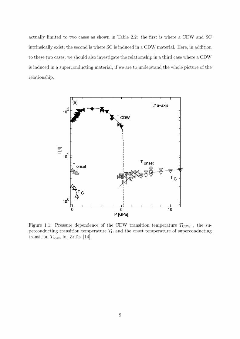
SC transition as shown in Fig. 1.1 [14]. On the other hand, the CDW is suppressed above
2 GPa while the SC transition emerges again at ∼5 GPa. Moreover, in NbSe3 with a
typical CDW material, Ta doping suppresses two CDWs and induces the SC transitionas
as shown in Fig. 1.2 [15]. These results show that the CDW or the SC is enhanced
while the other is suppressed, which is ascribed to the competition between the CDW
and SC on a Fermi surface. On the other hand, in a CuxTiSe2 system where Cu atoms
are doped in 1T -TiSe2 with a commensurate CDW material, a unique CDW and SC
phase diagram is observed as shown in Fig. 1.3 and a new relationship between CDW
and SC has been discussed [5, 16, 17]. According to the temperature dependence of the
resistance, the CDW is suppressed by Cu doping while SC is induced, and the dependence
of the SC transition temperature (TC) on Cu concentration has a domelike structure [5].
However, precise measurements performed with scanning tunneling microscopy (STM)
and X-ray diffraction (XRD) reveal that short-range order CDWs survive up to high Cu
concentrations where the SC emerges and the transition temperature of the short-range
order CDWs is independent of the TC [16, 17]. This result suggests that short-range order
CDWs are not necessarily in competition with SC and cannot be explained solely in terms
of the competition for the density of states at the Fermi level. Moreover, according to the
XRD result, the short-range order CDWs change from commensurate to incommensurate
at the Cu concentration where SC emerges in CuxTiSe2 [17]. The result suggests that
the incommensuration of the CDWs may affect the relationship between the CDWs and
SC. However, the reason for this is unclear. As described above, the relationship between
CDW and SC has been investigated in many materials. However, previous studies were
8
actually limited to two cases as shown in Table 2.2: the first is where a CDW and SC
intrinsically exist; the second is where SC is induced in a CDWmaterial. Here, in addition
to these two cases, we should also investigate the relationship in a third case where a CDW
is induced in a superconducting material, if we are to understand the whole picture of the
relationship.
Figure 1.1: Pressure dependence of the CDW transition temperature TCDW , the su-perconducting transition temperature TC and the onset temperature of superconductingtransition Tonset for ZrTe3 [14].
9
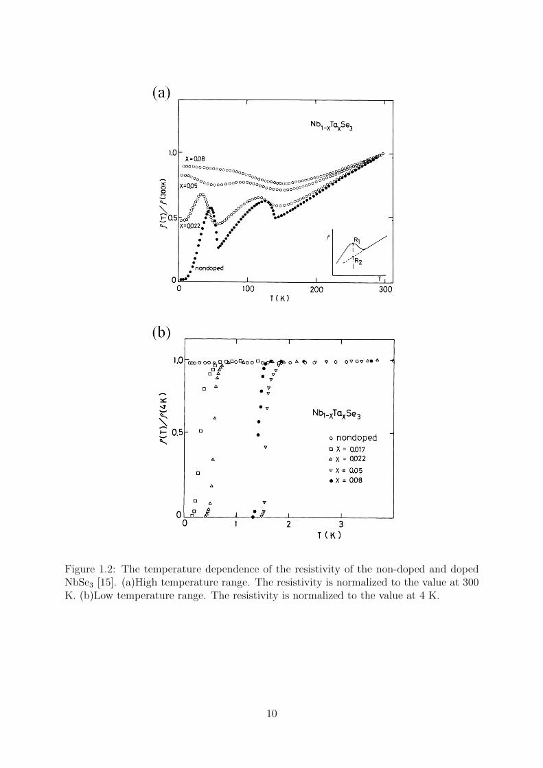
Figure 1.2: The temperature dependence of the resistivity of the non-doped and dopedNbSe3 [15]. (a)High temperature range. The resistivity is normalized to the value at 300K. (b)Low temperature range. The resistivity is normalized to the value at 4 K.
10
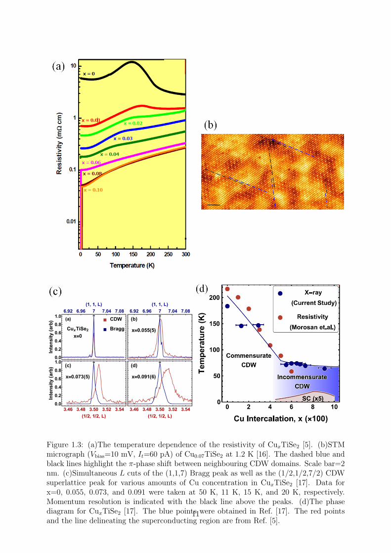
Figure 1.3: (a)The temperature dependence of the resistivity of CuxTiSe2 [5]. (b)STMmicrograph (Vbias=10 mV, It=60 pA) of Cu0.07TiSe2 at 1.2 K [16]. The dashed blue andblack lines highlight the π-phase shift between neighbouring CDW domains. Scale bar=2nm. (c)Simultaneous L cuts of the (1,1,7) Bragg peak as well as the (1/2,1/2,7/2) CDWsuperlattice peak for various amounts of Cu concentration in CuxTiSe2 [17]. Data forx=0, 0.055, 0.073, and 0.091 were taken at 50 K, 11 K, 15 K, and 20 K, respectively.Momentum resolution is indicated with the black line above the peaks. (d)The phasediagram for CuxTiSe2 [17]. The blue points were obtained in Ref. [17]. The red pointsand the line delineating the superconducting region are from Ref. [5].
11
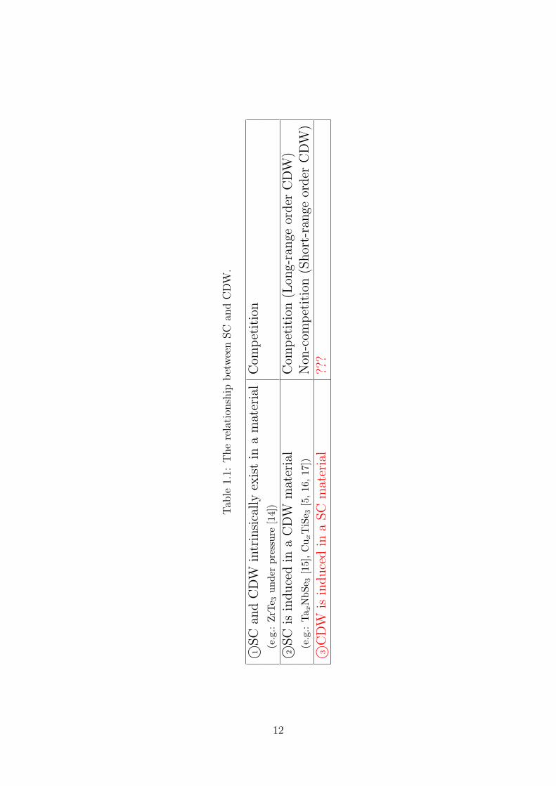
Tab
le1.1:
Therelation
ship
betweenSC
andCDW
.
1 ⃝SC
andCDW
intrinsicallyexistin
amaterial
Com
petition
(e.g.:ZrT
e 3under
pressure
[14])
2 ⃝SC
isinducedin
aCDW
material
Com
petition(Lon
g-range
order
CDW
)(e.g.:TaxNbSe 3
[15],CuxTiSe 3
[5,16
,17])
Non
-com
petition(Short-range
order
CDW
)3 ⃝CDW
isinducedin
aSC
material
???
12
1.3 Purpose of this study
In this thesis, we induced a CDW in a superconducting material and investigated the
relationship between the induced CDW and SC.
13
Chapter 2
Emergence of a CDW in Cu-dopedTaSe3
2.1 Introduction
2.1.1 TaSe3
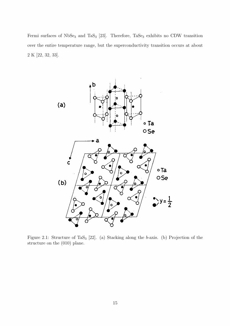
TaSe3 is a predominant candidate superconducting material capable of inducing a CDW.
TaSe3 is one of the transition metal trichalcogenides, MX3 (M: Nb, Ta; X: S, Se). MX3 has
a structure consisting of chains made of transition metals and chalcogens, and the chains
are weakly bonded by van der Waals forces [18, 19, 20, 21]. Figure 2.1 shows the structure
of TaSe3 [22]. Owing to this structure, MX3 is a quasi-one-dimensional conductor in which
an electric current travels well in the direction of the chain axis (b-axis). In most materials
belonging to MX3 (NbSe3, TaS3, and NbS3), the Fermi surface of is close to a plane [23]. If
the Fermi surface was translated by a wave vector, it would overlap well with that before
translation, i.e., the nesting condition is good. This indicates the intrinsic instability of
the Fermi surface, and as a result, a CDW develops below the transition temperature
as shown in Fig. 2.2 [24, 25, 26]. On the other hand, TaSe3 exhibits different properties
from the other MX3. TaSe3 is more three-dimensional than the other MX3 compounds.
Actually, the electrical conductivity anisotropy (σ∥ / σ⊥) of TaSe3 is 3–15, while that of
TaS3 is ∼100 and that of NbSe3 is 10–20 [28, 29, 30, 31]. Furthermore, according to
the band calculation, TaSe3 has two-dimensional Fermi surfaces, which are described as
fused tunnels running in the (−a∗ + c∗) direction in contrast to the one-dimensional flat
14
Fermi surfaces of NbSe3 and TaS3 [23]. Therefore, TaSe3 exhibits no CDW transition
over the entire temperature range, but the superconductivity transition occurs at about
2 K [22, 32, 33].
Figure 2.1: Structure of TaS3 [22]. (a) Stacking along the b-axis. (b) Projection of thestructure on the (010) plane.
15
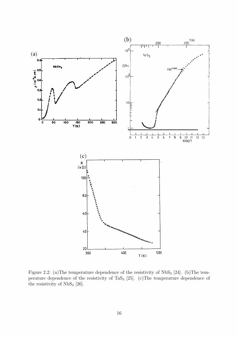
Figure 2.2: (a)The temperature dependence of the resistivity of NbS3 [24]. (b)The tem-perature dependence of the resistivity of TaS3 [25]. (c)The temperature dependence ofthe resistivity of NbS3 [26].
16
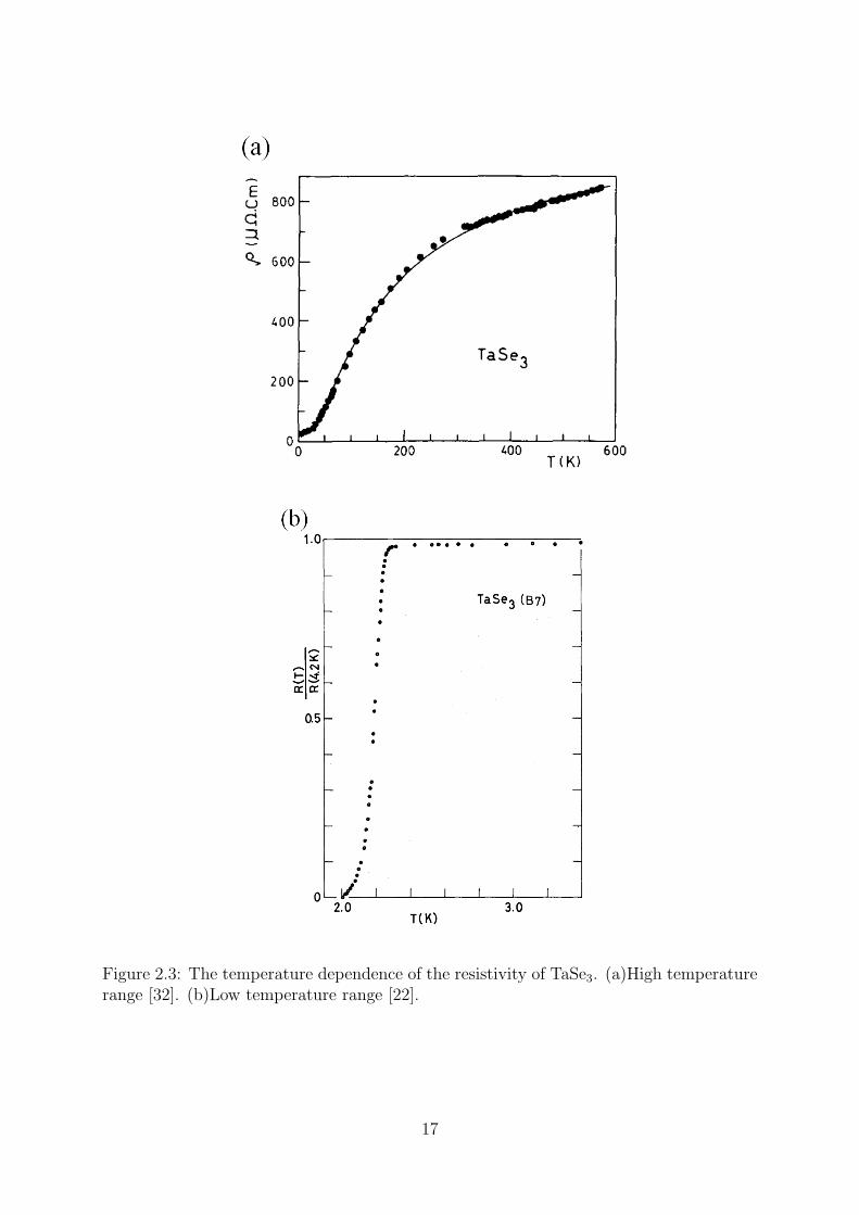
Figure 2.3: The temperature dependence of the resistivity of TaSe3. (a)High temperaturerange [32]. (b)Low temperature range [22].
17
2.1.2 Cu doping
There is Cu doping as a predominant candidate method capable of inducing a CDW in
TaSe3. If Cu atoms are doped in TaSe3, the Cu atoms are considered to be difficult to
substitute for Ta atoms because the common valence that Cu takes (+1 or +2) is different
from that of Ta (+5). On the other hand, because the TaSe3 chains are weakly bonded by
Van der Waals forces, the Cu atoms are expected to enter in the Van der Waals gap and to
increase the distance between chains. Actually, in CuxTiSe2 where TiSe2 layers are weakly
bonded by Van der Waals forces, Cu atoms enter between layers and increase the distance
between layers [5, 16]. Therefore, it is presumed that Cu doping for TaSe3 decreases the
overlap between electron wave functions perpendicular to the chain axis, leading to a
decrease in dimensionality. As a result, the nesting condition may be improved.
2.1.3 Purpose of this study
In this chapter, we tried to induce a CDW in TaSe3 with a superconducting material by
Cu doping, and investigated the presence of a CDW by measuring the resistance as a
function of temperature.
18
2.2 Experimental
2.2.1 Synthesis of single crystals
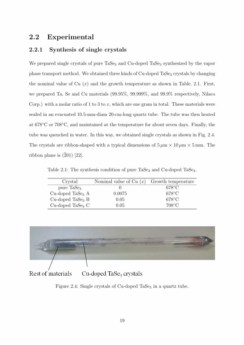
We prepared single crystals of pure TaSe3 and Cu-doped TaSe3 synthesized by the vapor
phase transport method. We obtained three kinds of Cu-doped TaSe3 crystals by changing
the nominal value of Cu (x) and the growth temperature as shown in Table. 2.1. First,
we prepared Ta, Se and Cu materials (99.95%, 99.999%, and 99.9% respectively, Nilaco
Corp.) with a molar ratio of 1 to 3 to x, which are one gram in total. These materials were
sealed in an evacuated 10.5-mm-diam 20-cm-long quartz tube. The tube was then heated
at 678C or 708C, and maintained at the temperature for about seven days. Finally, the
tube was quenched in water. In this way, we obtained single crystals as shown in Fig. 2.4.
The crystals are ribbon-shaped with a typical dimensions of 5µm× 10µm× 5mm. The
ribbon plane is (201) [22].
Table 2.1: The synthesis condition of pure TaSe3 and Cu-doped TaSe3.
Crystal Nominal value of Cu (x) Growth temperaturepure TaSe3 0 678C
Cu-doped TaSe3 A 0.0075 678CCu-doped TaSe3 B 0.05 678CCu-doped TaSe3 C 0.05 708C
Figure 2.4: Single crystals of Cu-doped TaSe3 in a quartz tube.
19
2.2.2 Inductively coupled plasma atomic emission spectroscopy
To examine the actual concentration of Cu in the crystals, we performed inductively
coupled plasma atomic emission spectroscopy (ICP-AES) using an ICPE-9000 (Shimadzu
Corp.). We determined the average Cu concentration for a bundle of the whisker crystals
(a few milligrams).
2.2.3 Single-crystal X-ray diffraction (XRD)
The crystal structure was examined by single-crystal X-ray diffraction (XRD) analysis
with Cu Kα radiation (λ = 1.5418 A) using a Rigaku XtaLAB P200 diffractometer. The
lattice parameters were extracted by fitting the XRD spectra using CrysAlisPro.
20
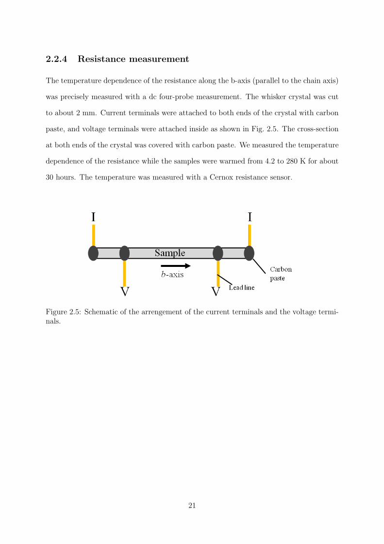
2.2.4 Resistance measurement
The temperature dependence of the resistance along the b-axis (parallel to the chain axis)
was precisely measured with a dc four-probe measurement. The whisker crystal was cut
to about 2 mm. Current terminals were attached to both ends of the crystal with carbon
paste, and voltage terminals were attached inside as shown in Fig. 2.5. The cross-section
at both ends of the crystal was covered with carbon paste. We measured the temperature
dependence of the resistance while the samples were warmed from 4.2 to 280 K for about
30 hours. The temperature was measured with a Cernox resistance sensor.
Figure 2.5: Schematic of the arrengement of the current terminals and the voltage termi-nals.
21
2.3 Results
2.3.1 Crystal
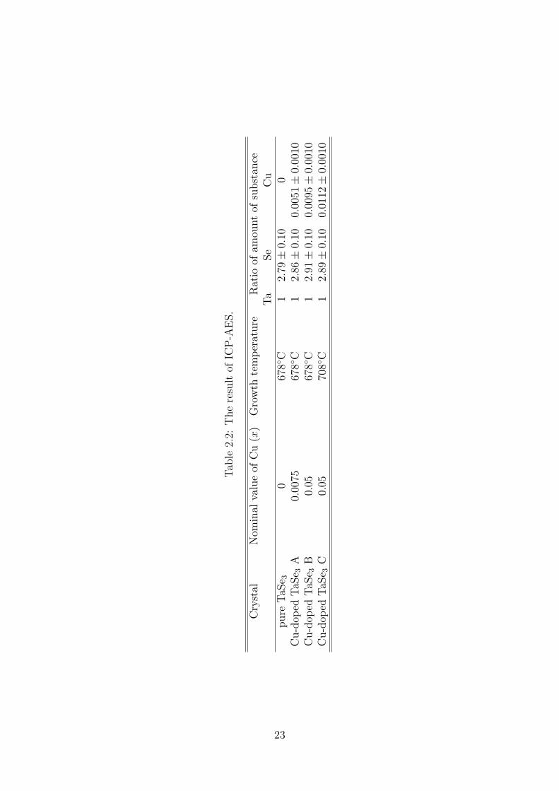
The result of ICP-AES are listed in Table 2.2. From the ratio of the amount of substance
determined by ICP-AES, we define the Cu concentration as the ratio of Cu to Ta given as a
percentage. The Cu concentrations of the Cu-doped TaSe3 were 0.51±0.10%, 0.95±0.10%
and 1.12 ± 0.10%. Thus, together with pure TaSe3, we prepared four kinds of crystals
with different Cu concentrations. The Cu concentration did not exceed 1.2% even when
the nominal value for Cu was more than 5%.
22
Tab
le2.2:
Theresultof
ICP-A
ES.
Crystal
Nom
inal
valueof
Cu(x)
Growth
temperature
Ratio
ofam
ountof
substan
ceTa
Se
Cu
pure
TaS
e 30
678C
12.79
±0.10
0Cu-dop
edTaS
e 3A
0.0075
678C
12.86
±0.10
0.0051
±0.0010
Cu-dop
edTaS
e 3B
0.05
678C
12.91
±0.10
0.0095
±0.0010
Cu-dop
edTaS
e 3C
0.05
708C
12.89
±0.10
0.0112
±0.0010
23
2.3.2 Result of single-crystal XRD
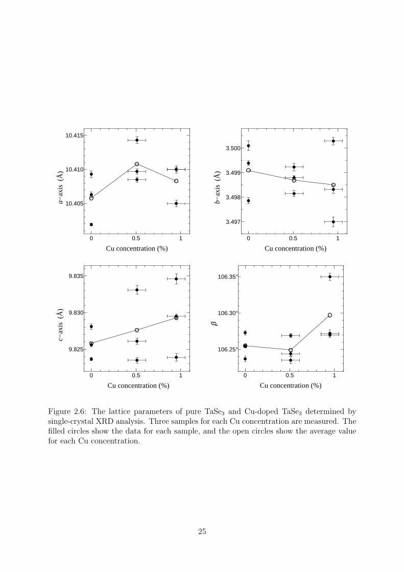
Figure 2.6 shows the lattice parameters determined by single-crystal XRD analysis as a
function of Cu concentration. The crystal structure of TaSe3 is monoclinic. The a-axis
and c-axis are perpendicular to the b-axis, which is the direction of the chain axis, and β
is the angle between the a-axis and the c-axis. The lattice parameters obtained for three
samples of pure TaSe3 were a = 10.402−10.409 A, b = 3.498−3.500 A, c = 9.824−9.828 A
and β = 106.24−106.27, which showed little sample dependence. However, the obtained
values were in good agreement with previously reported values of a = 10.402 ± 0.004 A,
b = 3.495 ± 0.002 A, c = 9.829 ± 0.004 A, β = 106.26 ± 0.03 [19], and a = 10.374 A,
b = 3.501 A, c = 9.827 A, β = 106.11 [34]. The lattice parameters we obtained for three
samples of each Cu-doped TaSe3 also exhibited sample dependence in almost the same
range as that of pure TaSe3. The Cu concentration dependence of lattice parameters
doesn’t show a clear change which satisfies Vegard’s law. However, the average values
for the a-axis, c-axis and β tended to increase slightly as the Cu concentration increased,
while that of the b-axis tended to decrease slightly.
24
0 0.5 1
10.405
10.410
10.415
Cu concentration (%)
a−ax
is (
Å)
0 0.5 1
3.497
3.498
3.499
3.500
Cu concentration (%)
b−ax
is (
Å)
0 0.5 1
9.825
9.830
9.835
Cu concentration (%)
c−ax
is (
Å)
0 0.5 1
106.25°
106.30°
106.35°
Cu concentration (%)
β
Figure 2.6: The lattice parameters of pure TaSe3 and Cu-doped TaSe3 determined bysingle-crystal XRD analysis. Three samples for each Cu concentration are measured. Thefilled circles show the data for each sample, and the open circles show the average valuefor each Cu concentration.
25
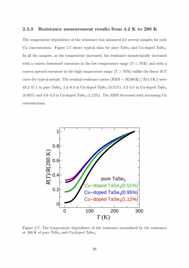
2.3.3 Resistance measurement results from 4.2 K to 280 K
The temperature dependence of the resistance was measured for several samples for each
Cu concentration. Figure 2.7 shows typical data for pure TaSe3 and Cu-doped TaSe3.
In all the samples, as the temperature increased, the resistance monotonically increased
with a convex downward curvature in the low temperature range (T < 70K) and with a
convex upward curvature in the high temperature range (T > 70K) unlike the linear R-T
curve for typical metals. The residual resistance ratios (RRR = R(280K) /R(4.5K)) were
43.2–57.1 in pure TaSe3, 5.3–6.3 in Cu-doped TaSe3 (0.51%), 3.2–3.5 in Cu-doped TaSe3
(0.95%) and 3.0–3.3 in Cu-doped TaSe3 (1.12%). The RRR decreased with increasing Cu
concentration.
0 100 200 3000
0.2
0.4
0.6
0.8
1
T (K)
R(T
)/R
(280
K)
pure TaSe3
Cu−doped TaSe3(0.95%)Cu−doped TaSe3(0.51%)
Cu−doped TaSe3(1.12%)
Figure 2.7: The temperature dependence of the resistance normalized by the resistanceat 280 K of pure TaSe3 and Cu-doped TaSe3.
26
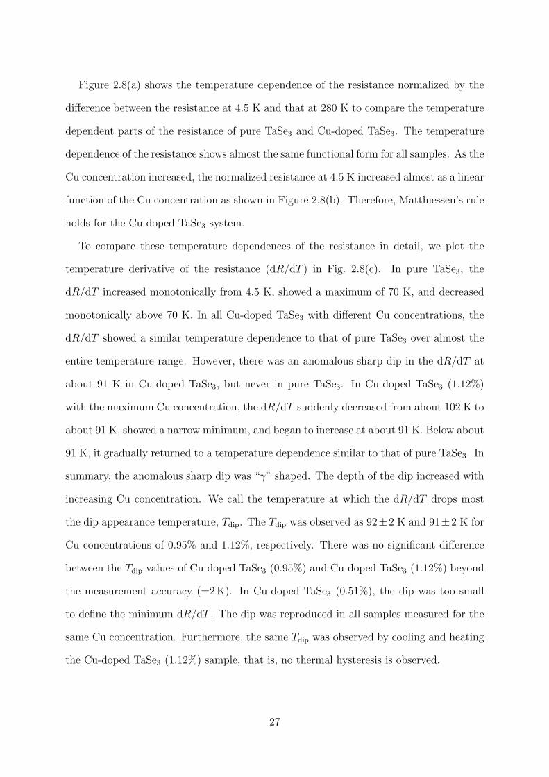
Figure 2.8(a) shows the temperature dependence of the resistance normalized by the
difference between the resistance at 4.5 K and that at 280 K to compare the temperature
dependent parts of the resistance of pure TaSe3 and Cu-doped TaSe3. The temperature
dependence of the resistance shows almost the same functional form for all samples. As the
Cu concentration increased, the normalized resistance at 4.5 K increased almost as a linear
function of the Cu concentration as shown in Figure 2.8(b). Therefore, Matthiessen’s rule
holds for the Cu-doped TaSe3 system.
To compare these temperature dependences of the resistance in detail, we plot the
temperature derivative of the resistance (dR/dT ) in Fig. 2.8(c). In pure TaSe3, the
dR/dT increased monotonically from 4.5 K, showed a maximum of 70 K, and decreased
monotonically above 70 K. In all Cu-doped TaSe3 with different Cu concentrations, the
dR/dT showed a similar temperature dependence to that of pure TaSe3 over almost the
entire temperature range. However, there was an anomalous sharp dip in the dR/dT at
about 91 K in Cu-doped TaSe3, but never in pure TaSe3. In Cu-doped TaSe3 (1.12%)
with the maximum Cu concentration, the dR/dT suddenly decreased from about 102 K to
about 91 K, showed a narrow minimum, and began to increase at about 91 K. Below about
91 K, it gradually returned to a temperature dependence similar to that of pure TaSe3. In
summary, the anomalous sharp dip was “γ” shaped. The depth of the dip increased with
increasing Cu concentration. We call the temperature at which the dR/dT drops most
the dip appearance temperature, Tdip. The Tdip was observed as 92±2 K and 91±2 K for
Cu concentrations of 0.95% and 1.12%, respectively. There was no significant difference
between the Tdip values of Cu-doped TaSe3 (0.95%) and Cu-doped TaSe3 (1.12%) beyond
the measurement accuracy (±2K). In Cu-doped TaSe3 (0.51%), the dip was too small
to define the minimum dR/dT . The dip was reproduced in all samples measured for the
same Cu concentration. Furthermore, the same Tdip was observed by cooling and heating
the Cu-doped TaSe3 (1.12%) sample, that is, no thermal hysteresis is observed.
27
0 100 200 300
0
0.5
1
1.5
T (K)
R(T
)
pure TaSe3
Cu−doped TaSe3(0.95%)Cu−doped TaSe3(0.51%)
Cu−doped TaSe3(1.12%)
R(2
80 K
)−R
(4.5
K)
(a)
0 0.5 10
0.1
0.2
0.3
0.4
0.5
R(4
.5 K
)R
(280
K)−
R(4
.5 K
)Cu concentration (%)
(b)
0 100 200 3000
2
4
6
8
T (K)
dR(T
)/dT
pure TaSe3
Cu−doped TaSe3(0.95%)Cu−doped TaSe3(0.51%)
Cu−doped TaSe3(1.12%)
R(2
80 K
)−R
(4.5
K)
(103 K
−1 )
(c)
Figure 2.8: (a)The temperature dependence of the resistance normalized by the differencebetween the resistance at 4.5 K and that at 280 K of pure TaSe3 and Cu-doped TaSe3.(b)The resistance at 4.5 K normalized by the difference between the resistance at 4.5 Kand that at 280 K as a function of Cu concentration. The average value is shown for eachCu concentration. (c)The temperature derivative of the normalized resistance in panel(a). The curves of Cu-doped TaSe3 (0.51%), Cu-doped TaSe3 (0.95%) and Cu-dopedTaSe3 (1.12%) are shifted vertically by 0.001, 0.002 and 0.003 K−1, respectively.
28
2.4 Discussion
2.4.1 Change in the lattice parameters by Cu doping
The single-crystal XRD analysis shows that the lattice parameters have sample depen-
dence and do not show Vegard’s law clearly for increasing Cu concentration, as shown in
Fig. 2.6. On the other hand, the RRR and the depth of the dip change systematically as
the Cu concentration increases (see Fig. 2.7 and Fig. 2.8(c)). The beam-diameter used
in the single-crystal XRD analysis is 0.15 mm and, as a result, the lattice parameters
are determined as the average value over a local region of 0.15 mm in comparison with
the resistance that is obtained as the average value over the region of 1–3 mm between
the voltage terminals. Thus, the inhomogeneity in a single crystal may cause the sam-
ple dependence of the lattice parameters. However, the inhomogeneous distribution of
Cu atoms is not the main cause because the sample dependence is observed not only in
Cu-doped TaSe3 but also in pure TaSe3. The ideal value of the molar ratio of Se to Ta
is 3. However, the actual molar ratio obtained using ICP-AES is 2.8–2.9 as shown in
Table 2.2. This fact shows excess Ta atoms or Se vacancies. It is possible that there
is inhomogeneous distribution of Ta and Se atoms in a single crystal which disturbs the
lattice parameters and obscures the effect of Cu-doping, i.e., Vegard’s law.
Therefore, we focus on the average value of the lattice parameter for each Cu concen-
tration and discuss the change in lattice parameters by Cu-doping. As shown in Fig. 2.6,
the average lattice parameter value tends to increase on the a-axis and c-axis (perpendic-
ular to the chain axis) and tends to decrease on the b-axis (parallel to the chain axis) as
the Cu concentration increases. The expansion of the a-axis and c-axis indicates that Cu
atoms may be intercalated in the Van der Walls gap between chains. When the distance
between chains is increased, and the chain axis is contracted, the dimensionality is ex-
pected to decrease because the overlap between wave functions perpendicular to the chain
axis decreases and that in the chain axis direction increases. Therefore, the result of the
29
single-crystal XRD analysis implies that the change in lattice parameters caused by Cu-
doping changes the Fermi surfaces from two-dimensional tunnel-like to one-dimensional
flat. This would lead to a better nesting condition in Cu-doped TaSe3 than in pure TaSe3.
2.4.2 Change in the number of carriers by Cu doping
In addition, we can consider the number of carriers to be another physical quantity that is
changed by Cu-doping. It is reported that the Cu atoms intercalated in the Van der Waals
gap are donors contributing delocalized electrons at the Fermi level [16]. The Cu atoms
in Cu-doped TaSe3 are assumed to be intercalated in Van der Waals gaps, and contribute
delocalized electrons. TaSe3 is a semimetal with several Fermi surfaces which consist of
a hole and an electron band [23]. In addition, the result of angle-resolved photoemission
spectroscopy (ARPES) exhibits a high density of states near the Fermi level [31]. Thus,
the density of states at the Fermi energy and the form of the Fermi surfaces are sensitive
to a change in the number of carriers. It is possible that the change in the number of
carriers caused by Cu-doping can also change the nesting condition although it does not
necessarily get better.
2.4.3 “γ”-shaped dip
We find an anomalous sharp dip in the dR/dT value in the temperature dependence
of the dR/dT of Cu-doped TaSe3, which is never observed in that of pure TaSe3, as
shown in Fig. 2.8(c). The dip in dR/dT is “γ” shaped with a sudden decrease and a
narrow minimum. Thus, the dip suggests a sudden change in state. The emergence of a
structural transition is suggested in pure TaSe3 under uniaxial strain [35]. However, the
sudden change in state in Cu-doped TaSe3 would not be a first-order transition because
we observe no thermal hysteresis.
We discuss how the resistance changes in the vicinity of the temperature where a dip in
dR/dT is present in Cu-doped TaSe3. When the dR/dT drops, the decrease in resistance
caused by the decrease in temperature is suppressed. Thus, the resistance below the
30
onset temperature of the dip (102 K) is larger than the resistance extrapolated from the
resistance-temperature curve above 102 K assuming that there is no dip in dR/dT . In
summary, the dip in dR/dT means a relative increase in resistance. MX3 compounds
(NbSe3, TaS3, NbS3) other than TaSe3 show anomalous increases in resistance at the
CDW transition temperatures (TCDW) because the whole or part of the Fermi surfaces
disappears and the number of carriers decreases [24, 25, 26]. Therefore, the sudden change
in state with a resistance increase in Cu-doped TaSe3 is most likely to be a CDW formation
although the resistance increase is relative.
We discuss the “γ”-shaped dip discovered in Cu-doped TaSe3 by comparison with the
temperature dependence of the dR/dT in CDW conductors such as NbSe3 [36], DyTe3 [37],
HfTe3 [38] and ZrTe3 [39]. These CDW conductors show the metallic temperature depen-
dence of the resistance in the normal state above the TCDW, and the resistance increase
at the TCDW. However, the temperature dependence of the resistance shows metallic
behavior again at lower temperatures because the Fermi surfaces partly remain due to
imperfect nesting. Although the magnitude of the resistance increase at TCDW is different
for the four CDW conductors, we find out a common dip in the dR/dT value correspond-
ing to the resistance increase as shown in Fig. 2.9 and Fig. 2.10. The dR/dT is constant
above the TCDW, however with decreasing temperature, it falls sharply at the TCDW and
then starts to increase at the minimum point. At lower temperatures, it increases more
gradually with a convex upward curvature and approaches a certain value. In short, the
temperature dependence of the dR/dT shows the common “γ”-shaped dip, indicating the
universal law peculiar to the CDW formation. The law states that a CDW is formed with
an energy gap opening on a Fermi surface. In the BCS theory on the CDW formation,
the energy gap opens at TCDW and grows obeying the temperature dependence of the gap
function. The opening and growth of the CDW gap reduce the number of conducting
carriers with decreasing temperature, leading to an increase in resistance near TCDW, and
at the same time the dR/dT has a “γ”-shaped dip. Actually, we can reproduce the “γ”-
31
shaped dip by calculation as described in Appendix. This fact strongly indicates that the
“γ”-shaped dip observed in Cu-doped TaSe3 is caused by the CDW formation.
As shown in Fig. 2.8(c), the Tdip of Cu-doped TaSe3 is about 91 K, which is lower than
the TCDW of the other MX3 compounds (340 K in NbS3 [26], 218 K in TaS3 [29], and 145
K in NbSe3 [24]). Originally pure TaSe3 has two-dimensional Fermi surfaces [23], where
the nesting condition is the worst in MX3 compounds, thus it shows no CDW formation.
Even if Fermi surfaces change and a CDW emerges in TaSe3, the temperature at which a
CDW forms is expected to be lower than the TCDW of the other MX3. Therefore, it will
be consistent to assume that Tdip in Cu-doped TaSe3 corresponds to the temperature of
the CDW formation.
32
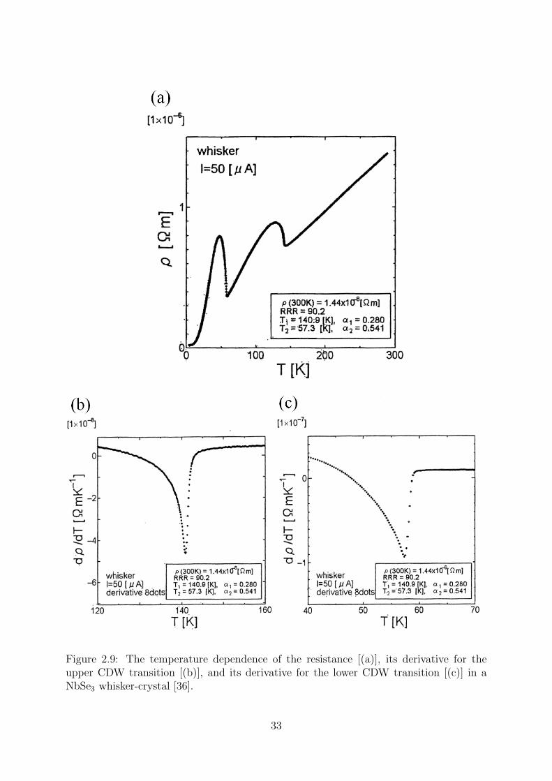
Figure 2.9: The temperature dependence of the resistance [(a)], its derivative for theupper CDW transition [(b)], and its derivative for the lower CDW transition [(c)] in aNbSe3 whisker-crystal [36].
33
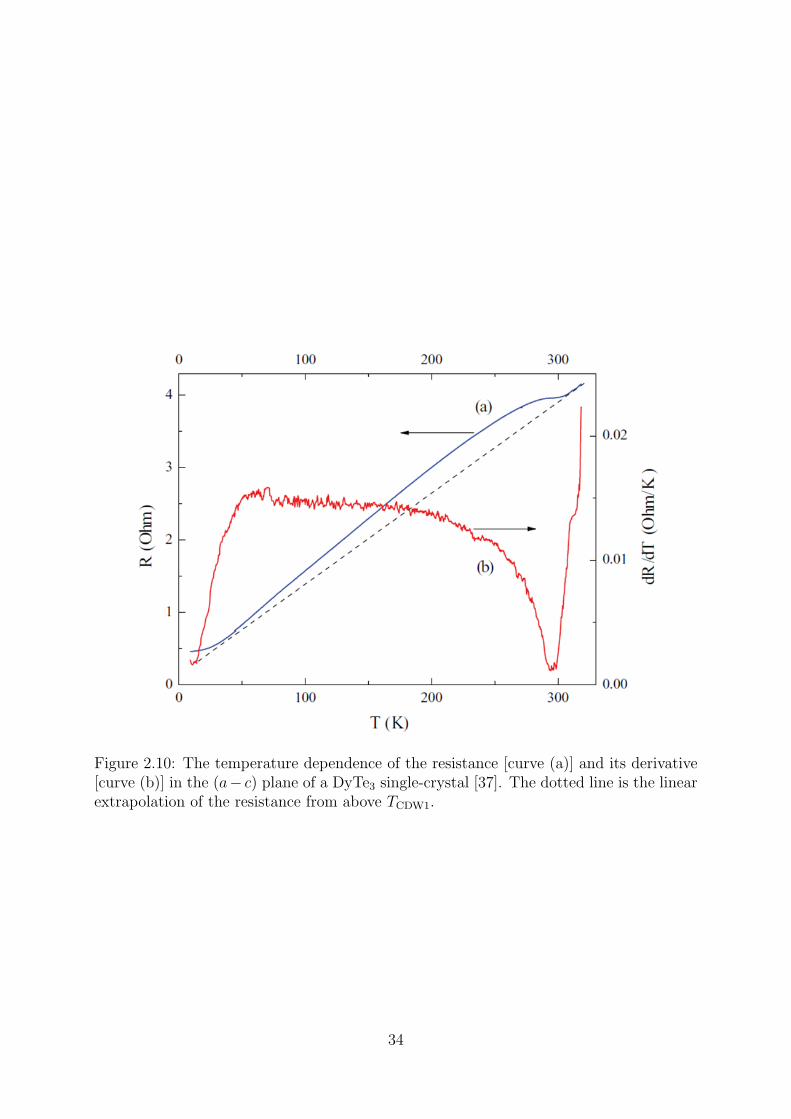
Figure 2.10: The temperature dependence of the resistance [curve (a)] and its derivative[curve (b)] in the (a− c) plane of a DyTe3 single-crystal [37]. The dotted line is the linearextrapolation of the resistance from above TCDW1.
34
2.4.4 Emergence of a CDW
From the discussions above, the main features of the Cu-doped TaSe3 system are summa-
rized as follows: i)The change in the lattice parameters caused by Cu-doping may change
the form of Fermi surfaces which leads to a better nesting condition. ii)The dip in dR/dT
exhibits a sudden change in state with a relative increase in resistance. iii)The dip in
dR/dT is “γ”-shaped and the same “γ”-shaped dip is commonly observed in many CDW
conductors. Therefore, we can conclude that a CDW emerges by Cu doping in TaSe3.
2.4.5 The CDW formation in the saddle-point mechanism
The above discussions about the CDW formation are based on the scenario of the Fermi
surface nesting. However, the resistance increase seen in Cu-doped TaSe3 is extremely
small, suggesting alternative scenario for the CDW formation. Rice and Scott propose
that Fermi surfaces with saddle points can be unstable against CDW formation [40]. In
this model, only a relatively small area of Fermi surfaces disappears and a large area
of those remains. Furthermore, the saddle points act as scattering sinks in the high-
temperature phase above TCDW and the conductivity can be enhanced at the TCDW by
the disappearance of the saddle points. As a result, the resistance increase due to the
CDW formation is suppressed. Therefore, the present result suggests the possibility that
the CDW formation is driven by the mechanism of Rice and Scott. Although the presence
of saddle points in pure TaSe3 is not mentioned by the result of the band calculation [23],
the result of ARPES shows that there is the flat band region with a high density of states
near the Fermi level in pure TaSe3 [31]. This singularity might drive the CDW formation
in Cu-doped TaSe3. In order to verify this mechanism, the band structure of Cu-doped
TaSe3 has to be investigated by ARPES.
35
2.5 Conclusion
By measuring precisely the temperature dependence of the resistance in pure TaSe3 and
Cu-doped TaSe3, we discovered an anomalous sharp dip in the temperature dependence
of the temperature derivative of the resistance (dR/dT ) in Cu-doped TaSe3, which was
never observed in pure TaSe3. The dip suggests that there is a sudden change in state
with a relative increase in resistance. Furthermore, the dip was “γ” shaped. We reveal
that many CDW conductors commonly exhibit the same “γ”-shaped dip in dR/dT at
the CDW transition temperature, which is a universal consequence of the opening and
growth of a CDW gap on a Fermi surface. Furthermore, the result of the single-crystal
X-ray diffraction (XRD) analysis implied that Cu doping increased the lattice parameter
of the a-axis and c-axis and decreased that of the b-axis, leading to an improvement in
the nesting condition. From the “γ”-shaped dip and the result of the single-crystal XRD
analysis, we conclude that a CDW emerges by Cu doping in TaSe3. Further studies are
needed to obtain direct evidence of the CDW formation.
36
Chapter 3
Superconductivity in Cu-dopedTaSe3
3.1 Introduction
In chapter 2, we concluded that a CDW is induced by Cu doping in TaSe3. On the other
hand, TaSe3 intrinsically exhibits the SC transition at about 2 K [22, 32, 33]. The SC
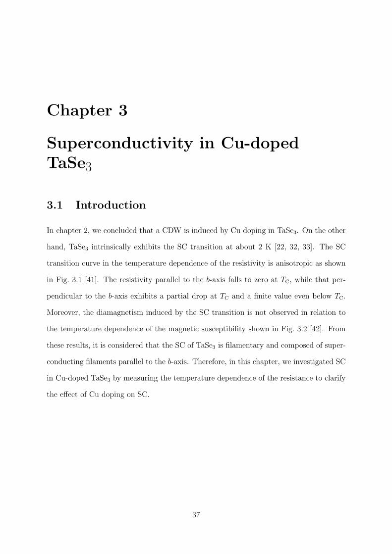
transition curve in the temperature dependence of the resistivity is anisotropic as shown
in Fig. 3.1 [41]. The resistivity parallel to the b-axis falls to zero at TC, while that per-
pendicular to the b-axis exhibits a partial drop at TC and a finite value even below TC.
Moreover, the diamagnetism induced by the SC transition is not observed in relation to
the temperature dependence of the magnetic susceptibility shown in Fig. 3.2 [42]. From
these results, it is considered that the SC of TaSe3 is filamentary and composed of super-
conducting filaments parallel to the b-axis. Therefore, in this chapter, we investigated SC
in Cu-doped TaSe3 by measuring the temperature dependence of the resistance to clarify
the effect of Cu doping on SC.
37
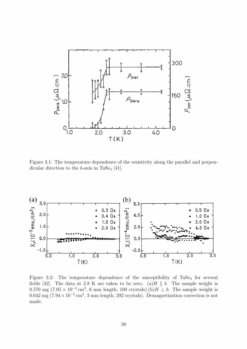
Figure 3.1: The temperature dependence of the resistivity along the parallel and perpen-dicular direction to the b-axis in TaSe3 [41].
Figure 3.2: The temperature dependence of the susceptibility of TaSe3 for severalfields [42]. The data at 2.8 K are taken to be zero. (a)H ∥ b. The sample weight is0.570 mg (7.05 × 10⁻⁵ cm3, 6 mm length, 100 crystals).(b)H ⊥ b. The sample weight is0.642 mg (7.94×10⁻⁵ cm3, 3 mm length, 292 crystals). Demagnetization correction is notmade.
38
3.2 Experimental
3.2.1 Synthesis of single crystals
We prepared single crystals of pure TaSe3 and Cu-doped TaSe3 synthesized by the vapor
phase transport method in the same way as chapter 2. The growth temperature was
660C as shown in Table. 3.1. The nominal value of Cu to Ta was 10% in Cu-doped
TaSe3. Crystals were ribbon-shaped with typical dimensions of 5µm × 10µm × 5mm.
The ribbon plane is (201) [22].
Table 3.1: The synthesis condition of pure TaSe3 and Cu-doped TaSe3.
Crystal Nominal value of Cu (x) Growth temperaturepure TaSe3 0 660C
Cu-doped TaSe3 0.1 660C
3.2.2 Resistance measurement
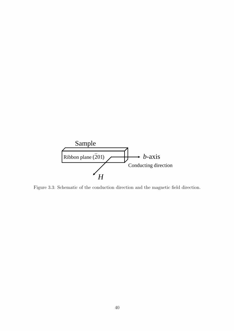
The temperature dependence of the resistance along the b-axis from 0.6 to 280 K was
measured with a dc four-probe technique. We placed the current terminals and the
voltage terminals as shown Fig 2.5. We measured the resistance while the samples were
being warmed from 2 to 280 K over about 30 hours and from 0.6 to 2 K over about 30
minutes. The measurements from 0.6 to 2 K were performed applying static magnetic
fields (0–80 mT) perpendicular to the ribbon plane as shown in Fig. 3.3 after the zero
field cooling.
39
b-axisRibbon plane
H
)012(
Conducting direction
Sample
Figure 3.3: Schematic of the conduction direction and the magnetic field direction.
40
3.3 Results
3.3.1 Resistance measurement results from 2 K to 280 K
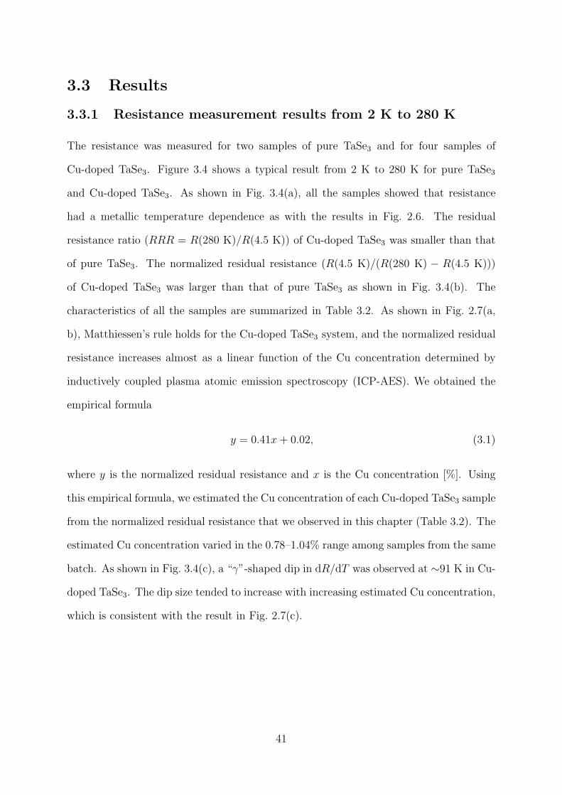
The resistance was measured for two samples of pure TaSe3 and for four samples of
Cu-doped TaSe3. Figure 3.4 shows a typical result from 2 K to 280 K for pure TaSe3
and Cu-doped TaSe3. As shown in Fig. 3.4(a), all the samples showed that resistance
had a metallic temperature dependence as with the results in Fig. 2.6. The residual
resistance ratio (RRR = R(280 K)/R(4.5 K)) of Cu-doped TaSe3 was smaller than that
of pure TaSe3. The normalized residual resistance (R(4.5 K)/(R(280 K) − R(4.5 K)))
of Cu-doped TaSe3 was larger than that of pure TaSe3 as shown in Fig. 3.4(b). The
characteristics of all the samples are summarized in Table 3.2. As shown in Fig. 2.7(a,
b), Matthiessen’s rule holds for the Cu-doped TaSe3 system, and the normalized residual
resistance increases almost as a linear function of the Cu concentration determined by
inductively coupled plasma atomic emission spectroscopy (ICP-AES). We obtained the
empirical formula
y = 0.41x+ 0.02, (3.1)
where y is the normalized residual resistance and x is the Cu concentration [%]. Using
this empirical formula, we estimated the Cu concentration of each Cu-doped TaSe3 sample
from the normalized residual resistance that we observed in this chapter (Table 3.2). The
estimated Cu concentration varied in the 0.78–1.04% range among samples from the same
batch. As shown in Fig. 3.4(c), a “γ”-shaped dip in dR/dT was observed at ∼91 K in Cu-
doped TaSe3. The dip size tended to increase with increasing estimated Cu concentration,
which is consistent with the result in Fig. 2.7(c).
41
0 100 200 300
0
0.5
1
T (K)
R(T
)/R
(280
K)
pure TaSe3 No.1
Cu−doped TaSe3 No.1
(a)
0 100 200 300
0
0.5
1
T (K)
R(T
)
pure TaSe3 No.1
Cu−doped TaSe3 No.1
R(2
80 K
)−R
(4.5
K)
(b)
0 100 200 300
0
2
4
6
8
T (K)
dR(T
)/dT
pure TaSe3 No.1
Cu−doped TaSe3 No.1
R(2
80 K
)−R
(4.5
K)
(103 K
−1 )
(c)
Figure 3.4: Typical resistance measurement results for pure TaSe3 and Cu-doped TaSe3from 2 K to 280 K. The normalization was in accordance with Fig. 2.7 and Fig. 2.8. (a)The temperature dependence of the resistance normalized by the resistance at 280 K.(b) The temperature dependence of the resistance normalized by the difference betweenthe resistances at 280 K and 4.5 K. (c) The temperature derivative of the normalizedresistance in panel (b). The curve of Cu-doped TaSe3 is shifted vertically by 0.001 K−1.
42
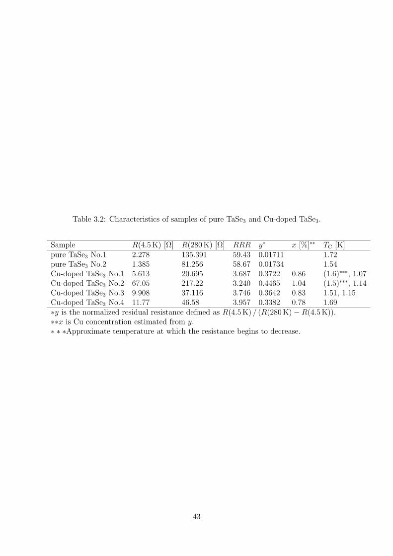
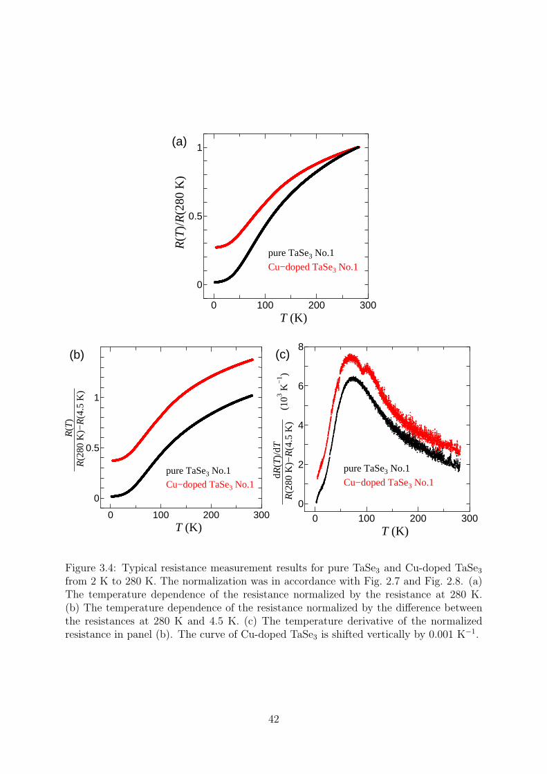
Table 3.2: Characteristics of samples of pure TaSe3 and Cu-doped TaSe3.
Sample R(4.5K) [Ω] R(280K) [Ω] RRR y∗ x [%]∗∗ TC [K]pure TaSe3 No.1 2.278 135.391 59.43 0.01711 1.72pure TaSe3 No.2 1.385 81.256 58.67 0.01734 1.54Cu-doped TaSe3 No.1 5.613 20.695 3.687 0.3722 0.86 (1.6)∗∗∗, 1.07Cu-doped TaSe3 No.2 67.05 217.22 3.240 0.4465 1.04 (1.5)∗∗∗, 1.14Cu-doped TaSe3 No.3 9.908 37.116 3.746 0.3642 0.83 1.51, 1.15Cu-doped TaSe3 No.4 11.77 46.58 3.957 0.3382 0.78 1.69∗y is the normalized residual resistance defined as R(4.5K) / (R(280K)−R(4.5K)).∗∗x is Cu concentration estimated from y.∗ ∗ ∗Approximate temperature at which the resistance begins to decrease.
43
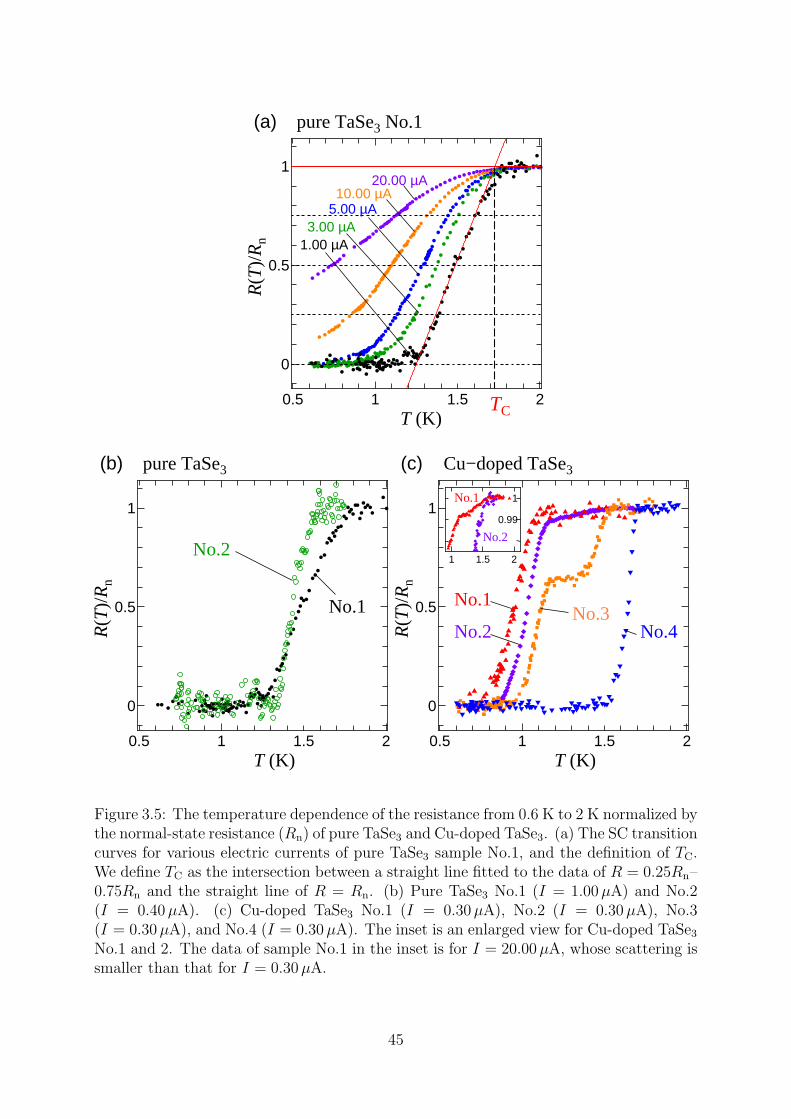
3.3.2 Resistance measurement results from 0.6 K to 2 K
Figure 3.5 shows the temperature dependence of the resistance of pure TaSe3 and Cu-
doped TaSe3 from 0.6 K to 2 K. All the samples of pure TaSe3 and Cu-doped TaSe3
exhibited a sharp drop in resistance due to the SC transition below 1.7 K. As shown in
Fig. 3.5(a), the SC transition exhibited electric current dependence, which matches the
results of previous studies [42, 43]. With increasing current, the onset of the SC transition
did not move while the offset shifted to the low-temperature side. Therefore, we determine
TC as defined in Fig. 3.5(a) from the SC transition curve observed for the smallest electric
current in this measurement. The SC transition temperatures (TCs) are summarized in
Table 3.2. Pure TaSe3 samples No.1 and 2 exhibited a one-step SC transition with a TC
of 1.54 K and 1.72 K, respectively. In Cu-doped TaSe3 samples No.1 and 2, the resistance
began to decrease at ∼1.6 K and 1.5 K, respectively, as shown in the inset of Fig. 3.5(c),
and droped mostly at 1.07 K and 1.14 K. Sample No.3 exhibited a two-step SC transition
with TCs of 1.51 K and 1.15 K. Sample No.4 exhibited a one-step SC transition with a TC
of ∼1.69 K. The ratio of the value of the drop in resistance at ∼1.1 K to the normal-state
resistance is ∼0.99 for No.1, ∼0.93 for No.2, ∼0.63 for No.3, and 0 for No.4. The samples
were No. 4, 3, 1 and 2 in ascending order of Cu concentration as shown in Table 3.2.
Thus, the ratio tended to be higher with increasing Cu concentration.
44
0.5 1 1.5 2
0
0.5
1
T (K)
R(T
)/R
n 1.00 µΑ3.00 µΑ
5.00 µΑ10.00 µΑ
20.00 µΑ
(a) pure TaSe3 No.1
TC
0.5 1 1.5 2
0
0.5
1
T (K)
R(T
)/R
n
No.1
No.2
(b) pure TaSe3
0.5 1 1.5 2
0
0.5
1
1 1.5 2
0.99
1
T (K)
R(T
)/R
n
No.3No.2
(c) Cu−doped TaSe3
No.1
No.2
No.4
No.1
Figure 3.5: The temperature dependence of the resistance from 0.6 K to 2 K normalized bythe normal-state resistance (Rn) of pure TaSe3 and Cu-doped TaSe3. (a) The SC transitioncurves for various electric currents of pure TaSe3 sample No.1, and the definition of TC.We define TC as the intersection between a straight line fitted to the data of R = 0.25Rn–0.75Rn and the straight line of R = Rn. (b) Pure TaSe3 No.1 (I = 1.00µA) and No.2(I = 0.40µA). (c) Cu-doped TaSe3 No.1 (I = 0.30µA), No.2 (I = 0.30µA), No.3(I = 0.30µA), and No.4 (I = 0.30µA). The inset is an enlarged view for Cu-doped TaSe3No.1 and 2. The data of sample No.1 in the inset is for I = 20.00µA, whose scattering issmaller than that for I = 0.30µA.
45
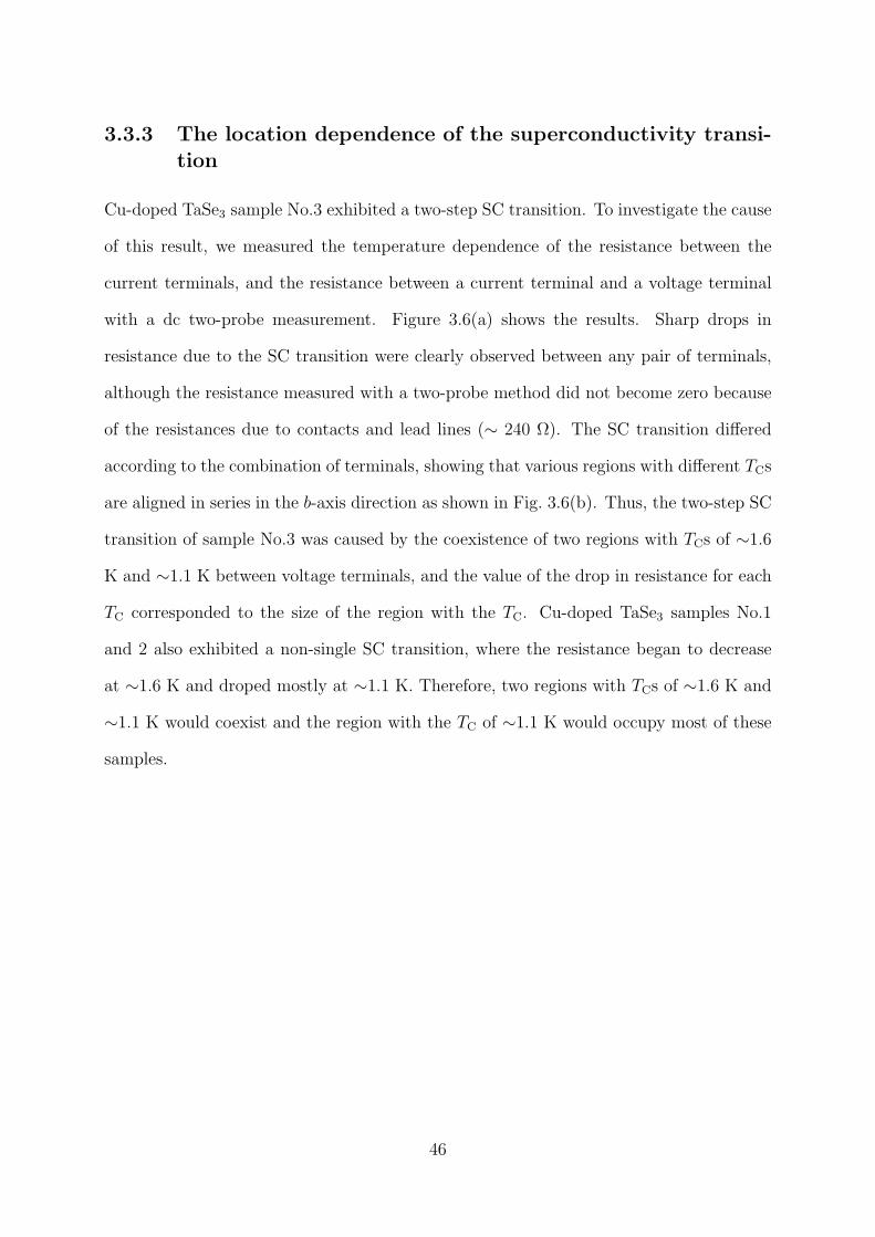
3.3.3 The location dependence of the superconductivity transi-tion
Cu-doped TaSe3 sample No.3 exhibited a two-step SC transition. To investigate the cause
of this result, we measured the temperature dependence of the resistance between the
current terminals, and the resistance between a current terminal and a voltage terminal
with a dc two-probe measurement. Figure 3.6(a) shows the results. Sharp drops in
resistance due to the SC transition were clearly observed between any pair of terminals,
although the resistance measured with a two-probe method did not become zero because
of the resistances due to contacts and lead lines (∼ 240 Ω). The SC transition differed
according to the combination of terminals, showing that various regions with different TCs
are aligned in series in the b-axis direction as shown in Fig. 3.6(b). Thus, the two-step SC
transition of sample No.3 was caused by the coexistence of two regions with TCs of ∼1.6
K and ∼1.1 K between voltage terminals, and the value of the drop in resistance for each
TC corresponded to the size of the region with the TC. Cu-doped TaSe3 samples No.1
and 2 also exhibited a non-single SC transition, where the resistance began to decrease
at ∼1.6 K and droped mostly at ∼1.1 K. Therefore, two regions with TCs of ∼1.6 K and
∼1.1 K would coexist and the region with the TC of ∼1.1 K would occupy most of these
samples.
46
0.5 1 1.5 2
0
5
10
15
20
240
245
250
255
T (K)
R(Ω
)I1−I2 (two−probe)
V2−I2 (two−probe)
I1−V1 (two−probe)
Cu−doped TaSe3 No.3 (I=0.30 µΑ)
V1−V2 (four−probe)
R(Ω
)
(a)
Sample
b-axis
Cu-doped TaSe3 No.3
Carbon paste
Lead line
TC~1.5 K TC~1.15 K TC~1.35 K
V2V1
I1 I2
Figure 3.6: (a) The temperature dependence of the resistance between the voltage ter-minals, between the current terminals, and between a current terminal and a voltageterminal in Cu-doped TaSe3 sample No.3. (b) Schematic of spatial distribution of TC inCu-doped TaSe3 sample No.3 derived from panel 4(a). However, the distribution of theregions with the TCs of ∼1.6 K and ∼1.15 K between the voltage terminals is deduced.
47
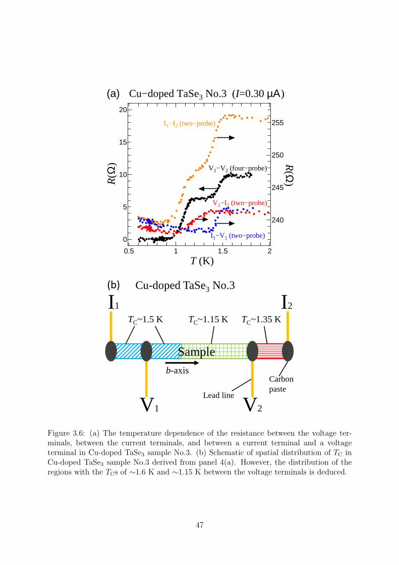
3.3.4 The superconductivity transition under static magneticfields
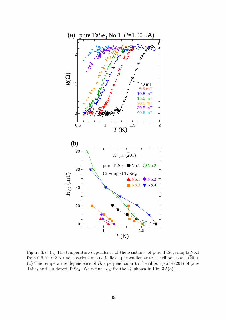
Figure 3.7(a) shows a typical temperature dependence of the resistance from 0.6 K to 2 K
under various magnetic fields perpendicular to the ribbon plane (201). As the magnetic
field increased, the SC transition curve shifted to the low-temperature side. Figure 3.7(b)
shows the temperature dependence of the upper critical field (HC2) perpendicular to the
ribbon plane (201) of pure TaSe3 and Cu-doped TaSe3. As the temperature decreased,
HC2 of pure TaSe3 sample No.1 increased with an upward curvature, and HC2 of pure
TaSe3 sample No.2 increased with temperature dependence as a linear function near TC
and with an upward curvature at low temperatures. HC2 of Cu-doped TaSe3 sample No.2
increased with an upward curvature, and HC2 of Cu-doped TaSe3 sample No.4 increased
with a downward curvature near TC of ∼1.6 K and with an upward curvature at low tem-
peratures. In Cu-doped TaSe3 sample No.3, HC2 for the first-step SC transition exhibited
an upward curvature and that for the second-step SC transition exhibited a slightly down-
ward curvature. The curvature for Cu-doped TaSe3 sample No.1 was unknown because
there were only two points.
48
0.5 1 1.5 2
0
1
2
T (K)
R(Ω
)
0 mT5.5 mT
10.5 mT15.5 mT20.5 mT
pure TaSe3 No.1 (I=1.00 µΑ)
30.5 mT40.5 mT
(a)
1 1.5
0
20
40
60
80HC2 (201)
HC
2 (m
T)
T (K)
pure TaSe3: No.1 No.2
Cu−doped TaSe3:No.2No.1
No.3 No.4
(b)
Figure 3.7: (a) The temperature dependence of the resistance of pure TaSe3 sample No.1from 0.6 K to 2 K under various magnetic fields perpendicular to the ribbon plane (201).(b) The temperature dependence of HC2 perpendicular to the ribbon plane (201) of pureTaSe3 and Cu-doped TaSe3. We define HC2 for the TC shown in Fig. 3.5(a).
49
3.4 Discussion
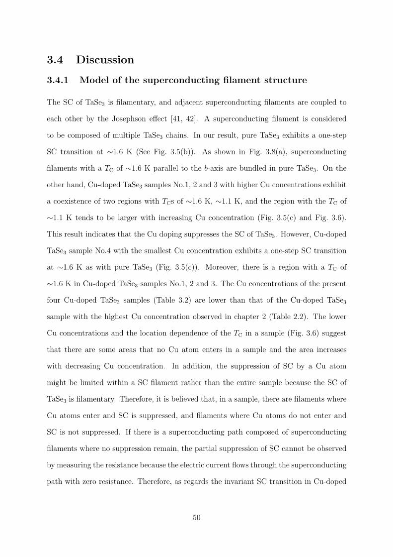
3.4.1 Model of the superconducting filament structure
The SC of TaSe3 is filamentary, and adjacent superconducting filaments are coupled to
each other by the Josephson effect [41, 42]. A superconducting filament is considered
to be composed of multiple TaSe3 chains. In our result, pure TaSe3 exhibits a one-step
SC transition at ∼1.6 K (See Fig. 3.5(b)). As shown in Fig. 3.8(a), superconducting
filaments with a TC of ∼1.6 K parallel to the b-axis are bundled in pure TaSe3. On the
other hand, Cu-doped TaSe3 samples No.1, 2 and 3 with higher Cu concentrations exhibit
a coexistence of two regions with TCs of ∼1.6 K, ∼1.1 K, and the region with the TC of
∼1.1 K tends to be larger with increasing Cu concentration (Fig. 3.5(c) and Fig. 3.6).
This result indicates that the Cu doping suppresses the SC of TaSe3. However, Cu-doped
TaSe3 sample No.4 with the smallest Cu concentration exhibits a one-step SC transition
at ∼1.6 K as with pure TaSe3 (Fig. 3.5(c)). Moreover, there is a region with a TC of
∼1.6 K in Cu-doped TaSe3 samples No.1, 2 and 3. The Cu concentrations of the present
four Cu-doped TaSe3 samples (Table 3.2) are lower than that of the Cu-doped TaSe3
sample with the highest Cu concentration observed in chapter 2 (Table 2.2). The lower
Cu concentrations and the location dependence of the TC in a sample (Fig. 3.6) suggest
that there are some areas that no Cu atom enters in a sample and the area increases
with decreasing Cu concentration. In addition, the suppression of SC by a Cu atom
might be limited within a SC filament rather than the entire sample because the SC of
TaSe3 is filamentary. Therefore, it is believed that, in a sample, there are filaments where
Cu atoms enter and SC is suppressed, and filaments where Cu atoms do not enter and
SC is not suppressed. If there is a superconducting path composed of superconducting
filaments where no suppression remain, the partial suppression of SC cannot be observed
by measuring the resistance because the electric current flows through the superconducting
path with zero resistance. Therefore, as regards the invariant SC transition in Cu-doped
50
TaSe3 sample No.4 and the region where TC does not change in samples No.1, 2 and 3, it
can be interpreted that more than one superconducting path with a TC of ∼1.6 K remains
as shown in Fig. 3.8(b, c). Inhomogeneous SC as observed in Cu-doped TaSe3 has been
extensively studied theoretically and experimentally in other systems [44, 45, 46].
TC~1.6 K TC~1.1 K
(a) pure TaSe3 (b) Cu-doped TaSe3 No. 4(lowest Cu concentration)
(c) Cu-doped TaSe3 No.1, 2, 3(higher Cu concentration)
superconducting filament
Cu atom
b-axis
Figure 3.8: Model of the SC filament structures of pure TaSe3 and Cu-doped TaSe3. TheTC of suppressed SC is represented by 1.1 K overall.
51
3.4.2 Change in the HC2-temperature curve by Cu doping
We compare the temperature dependence of HC2 for pure TaSe3 and Cu-doped TaSe3.
HC2 is derived from the Pauli paramagnetic and orbital effects. However, the Pauli
paramagnetic limit will not matter in the present range of magnetic fields (0–80 mT).
Considering orbital effects based on the Ginzburg-Landau (GL) theory, the temperature
dependence of the HC2 of bulk superconductors is expressed as
HC2(t) = HC2(0)1− t2
1 + t2, (3.2)
where t is the normalized temperature (t = T/TC). However, the temperature dependence
of the HC2 of pure TaSe3 and Cu-doped TaSe3 (Fig. 3.7(b)) cannot be expressed by
eq. 3.2. Thus, we require a theoretical model that considers the special feature of the
SC of TaSe3, namely filamentary SC. According to the GL theory of filamentary SC
proposed by L. A. Turkevich and R. A. Klemm (the TK theory), the HC2 for Josephson-
coupled superconducting filaments increases with an upward curvature as temperature
decreases [47]. On the other hand, the HC2 for decoupled superconducting filaments
increases with a downward curvature. The temperature dependence of theHC2 exhibits an
upward curvature in the two pure TaSe3 samples (Fig. 3.7(b)). From the TK theory, this
result implies the Josephson coupling of superconducting filaments. Even in our model,
as shown in Fig. 3.8(a), the SC of pure TaSe3 is composed of coupled superconducting
filaments with the same TC. In contrast, the temperature dependence of theHC2 exhibits a
downward curvature near a TC of ∼1.6 K in Cu-doped TaSe3 sample No.4 with the same
SC transition as pure TaSe3. Thus, according to the TK theory, the superconducting
filaments are decoupled near 1.6 K in this sample. This result is consistent with our
model shown in Fig. 3.8(b) where the superconducting filaments with a TC of ∼1.6 K
are sparse. In other Cu-doped TaSe3 samples No.2 and 3, the temperature dependence
of the HC2 exhibits an upward curvature or a downward curvature. Cu doping results
in superconducting filaments with different TCs being mixed in a sample as shown in
52
Fig. 3.8(c). As a result, there are regions where superconducting filaments with the
same TC are adjacent and coupled, and regions where superconducting filaments with
different TCs are adjacent and not coupled. This complex configuration of superconducting
filaments might lead to the complex sample dependence of the HC2-temperature curve.
53
3.5 Conclusion
We investigated SC in Cu-doped TaSe3 by measuring the temperature dependence of the
resistance. The Cu-doped TaSe3 sample with the smallest Cu concentration exhibited a
one-step SC transition with a TC of ∼1.6 K as well as pure TaSe3. On the other hand,
those with larger Cu concentrations exhibited a two-step SC transition with TCs of ∼1.6
K and ∼1.1 K, or a non-single SC transition where the resistance began to decrease at
∼1.6 K and droped mostly at ∼1.1 K. The value of the drop in resistance at ∼1.1 K
tended to expand with increasing Cu concentration. The location dependence of the SC
transition showed that the two-step SC transition and the non-single SC transition are
caused by the coexistence of two regions with TCs of ∼1.6 K and ∼1.1 K aligned in series
in the b-axis direction in a sample. The temperature dependence of the HC2 of Cu-doped
TaSe3 exhibits upward curvature or downward curvature while that of pure TaSe3 exhibits
upward curvature. From these SC results and the fact that the SC in TaSe3 is filamentary,
we conclude that SC is suppressed locally by Cu doping in all Cu-doped TaSe3 samples.
54
Chapter 4
Further discussion
4.1 Competitive relationship between superconduc-
tivity and the induced CDW
From the results in chapter 2, we found that a CDW emerges in Cu-doped TaSe3. On
the other hand, the SC intrinsically present in TaSe3 is suppressed by Cu doping from
the results in chapter 3. Hence, the induced CDW and SC would be in a competitive
relationship in Cu-doped TaSe3.
55
4.2 Short-range order of the induced CDW
We discuss the the induced CDW in Cu-doped TaSe3 because the CDW property is
important when discussing the relationship between SC and CDW. The SC suppression
of TaSe3 is local in the filament where Cu atoms enter as shown in Fig. 3.8. Therefore, it
is possible that there is no coherent CDW in the entire sample, but CDWs exist locally.
From the viewpoint of the locality of CDWs, we reconsider the resistance anomaly
results, that is, the “γ”-shaped dip in dR/dT due to the CDW formation in Cu-doped
TaSe3. Conventional CDW materials such as NbSe3, TaS3 and NbS3 exibit anomalous
increases in resistance at the TCDW) because all or part of the Fermi surface disappears
and the number of carriers decreases [24, 25, 26]. On the other hand, the resistance
anomaly of Cu-doped TaSe3 is extremely small as shown in Fig. 2.8(c). This result for
Cu-doped TaSe3 may arise because of the locality of the existence of the CDWs. In fact,
in CuxTiSe2, no signal due to the formation of short-range order CDWs is observed in
the temperature dependence of the resistance [5].
Moreover, a comparison of the “γ”-shaped dips of Cu-doped TaSe3 samples with differ-
ent Cu concentrations shows that the dip size increases with increasing Cu concentration
while the temperature at which the dip appears is almost constant as shown in Fig. 2.8(c).
The dip size corresponds to the area of the reduced Fermi surface, and the dip appear-
ance temperature corresponds to TCDW. The relationship between the dip size and the dip
appearance temperature appears to contradict the prediction for long-range order CDW
with the mean-field theory, which shows a positive correlation between the area of the
reduced Fermi surface and TCDW. However, if the induced CDWs have short-range order
in the vicinity of Cu atoms and the size of a CDW is shorter than the distance between Cu
atoms, we can interpret the conflicting result mentioned above consistently, namely that
the size increases with increasing Cu concentration because the number of short-range
order CDWs increases, while the appearance temperature is constant because the state
of each short-range order CDW is unchanged.
56
Here, we estimate the size of short-range order CDWs from a simple calculation of the
distance between Cu atoms. The volume of a unit cell of TaSe3 is estimated to be ∼0.34
nm3 from the lattice parameters determined in this study, and a unit cell contains four
Ta atoms. In addition, the Cu concentration of Cu-doped TaSe3 is at most 1%. Hence, if
Cu atoms enter a crystal evenly, each Cu atom enters a space of ∼8.5 (= 0.34/(4× 0.01))
nm3 and the distance between adjacent Cu atoms is estimated to be ∼2 nm. Therefore,
the CDW size must be shorter than ∼2 nm.
57
4.3 The effect of the pinning of CDWs on the re-
lationship between superconductivity and short-
range order CDWs
The estimated size of the CDWs in Cu-doped TaSe3 is on a nanometer-scale and com-
parable to the size of the short-range order CDWs in CuxTiSe2 [16]. In CuxTiSe2, the
short-range order CDWs do not compete with the SC transition. On the other hand, our
results suggest that short-range order CDWs compete with SC in Cu-doped TaSe3. One
of differences between the two materials is that the CDWs form on Cu atoms in Cu-doped
TaSe3 while the CDW is suppressed in the area where Cu atoms enter in CuxTiSe2 [16].
Generally, when there is an impurity, a CDW is pinned by that impurity [48]. Hence,
the CDWs in Cu-doped TaSe3 would be harder to move than those in CuxTiSe2. More-
over, in CuxTiSe2, the modulation period of the CDWs changes from commensurate to
incommensurate at the Cu concentration where the SC phase emerges [17]. In general, a
commensurate CDW is harder to move than an incommensurate CDW [48]. Therefore,
CDWs may compete with SC when CDWs are hard to move due to impurity pinning or
commensurate pinning. We should note that, when discussing the relationship between
SC and another electron ordering which is periodically modulated, there is a case where
whether the electron ordering is static or dynamic is important [49].
58
Chapter 5
Genaral conclusion
We measured precisely the temperature dependence of the resistance of Cu-doped TaSe3.
As a result, we discovered a “γ”-shaped dip in dR/dT at ∼91 K in Cu-doped TaSe3,
which was never observed in pure TaSe3. The dip suggests that there is a sudden change
in state with a relative increase in resistance. We reveal that many CDW conductors
commonly exhibit the same “γ”-shaped dip in dR/dT at the CDW transition temperature,
which is a universal consequence of the opening and growth of a CDW gap on a Fermi
surface. The result of the single-crystal XRD analysis implied that Cu doping increased
the lattice parameter of the a-axis and c-axis and decreased that of the b-axis, leading to
an improvement in the nesting condition. Based on the “γ”-shaped dip and the result
of the single-crystal XRD analysis, we conclude that a CDW emerges by Cu-doping in
TaSe3.
We investigated the effect of Cu doping on SC in Cu-doped TaSe3. In pure TaSe3
and Cu-doped TaSe3 sample with the smallest Cu concentration, the SC transition has
a step with a TC of ∼1.6 K. On the other hand, in Cu-doped samples with larger Cu
concentrations exhibited a two-step SC transition with TCs of ∼1.6 K and ∼1.1 K, or a
non-single SC transition where the resistance began to decrease at ∼1.6 K and droped
mostly at ∼1.1 K. The ratio of the drop in resistance at ∼1.1 K tended to expand with
increasing Cu concentration. The location dependence of the SC transition in a sample
showed that the two-step SC transition and the non-single SC transition are caused by the
59
coexistence of two regions with TCs of ∼1.6 K and ∼1.1 K aligned in series in the b-axis
direction. The HC2-temperature curve of Cu-doped TaSe3 exhibits upward curvature or
downward curvature while that of pure TaSe3 exhibits upward curvature. From these SC
results and the fact that the SC in TaSe3 is filamentary, we conclude that SC is suppressed
locally by Cu doping.
The above results show that a CDW is induced while SC is suppressed in Cu-doped
TaSe3. Therefore, the induced CDW and SC are in a competitive relationship.
The locality of SC suppression suggests that the induced CDWs are local. The increase
in resistance due to the CDW transition was extremely small. In addition, as the Cu
concentration increased, the size of the “γ”-shaped dip was enhanced but the temperature
at which the dip appeared hardly changed. These results of the induced CDW transition
can consistently be interpreted from the short-range order which the induced CDWs in
the vicinity of Cu atoms have.
From all the discussions, we conclude that the induced short-range order CDWs and
SC are in a competitive relationship in Cu-doped TaSe3. On the other hand, it was
previously reported that short-range order CDWs and SC do not compete in CuxTiSe2
where SC is induced in a CDW material. By comparing the detailed experimental results
of these two materials, we will clarify the physics that defines the relationship between
short-range order CDWs and SC.
60
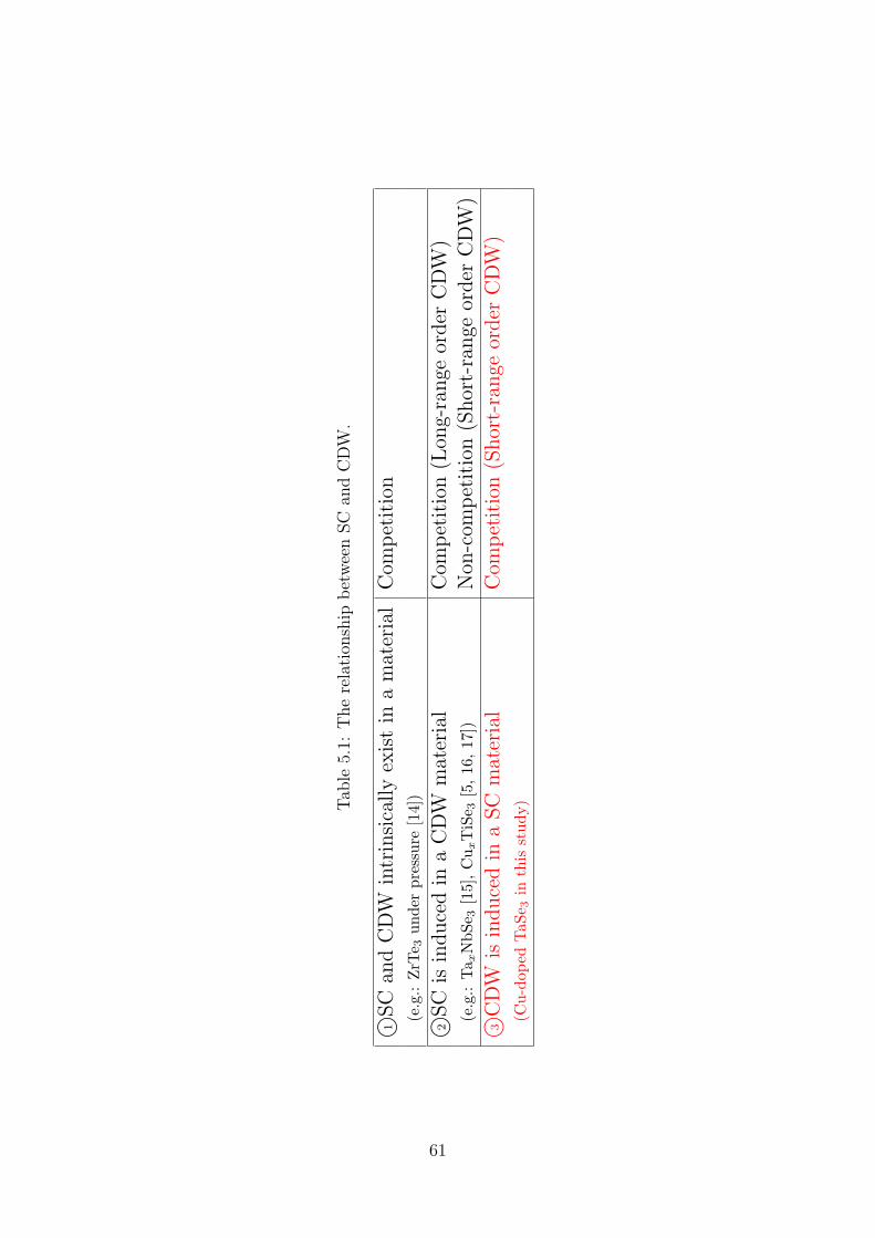
Tab
le5.1:
Therelation
ship
betweenSC
andCDW
.
1 ⃝SC
andCDW
intrinsicallyexistin
amaterial
Com
petition
(e.g.:ZrT
e 3under
pressure
[14])
2 ⃝SC
isinducedin
aCDW
material
Com
petition(Lon
g-range
order
CDW
)(e.g.:TaxNbSe 3
[15],CuxTiSe 3
[5,16
,17])
Non
-com
petition(Short-range
order
CDW
)3 ⃝CDW
isinducedin
aSC
material
Com
petition(Short-range
order
CDW
)(C
u-dop
edTaS
e 3in
this
study)
61
Appendix
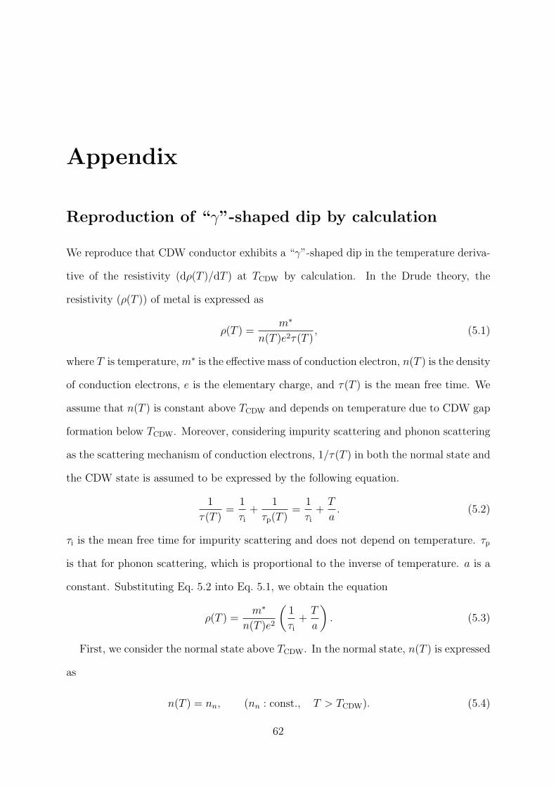
Reproduction of “γ”-shaped dip by calculation
We reproduce that CDW conductor exhibits a “γ”-shaped dip in the temperature deriva-
tive of the resistivity (dρ(T )/dT ) at TCDW by calculation. In the Drude theory, the
resistivity (ρ(T )) of metal is expressed as
ρ(T ) =m∗
n(T )e2τ(T ), (5.1)
where T is temperature, m∗ is the effective mass of conduction electron, n(T ) is the density
of conduction electrons, e is the elementary charge, and τ(T ) is the mean free time. We
assume that n(T ) is constant above TCDW and depends on temperature due to CDW gap
formation below TCDW. Moreover, considering impurity scattering and phonon scattering
as the scattering mechanism of conduction electrons, 1/τ(T ) in both the normal state and
the CDW state is assumed to be expressed by the following equation.
1
τ(T )=
1
τi+
1
τp(T )=
1
τi+
T
a. (5.2)
τi is the mean free time for impurity scattering and does not depend on temperature. τp
is that for phonon scattering, which is proportional to the inverse of temperature. a is a
constant. Substituting Eq. 5.2 into Eq. 5.1, we obtain the equation
ρ(T ) =m∗
n(T )e2
(1
τi+
T
a
). (5.3)
First, we consider the normal state above TCDW. In the normal state, n(T ) is expressed
as
n(T ) = nn, (nn : const., T > TCDW). (5.4)
62
Substituting Eq. 5.4 into Eq. 5.3, we obtain the ρ(T ) in the normal state
ρ(T ) =m∗
nne2
(1
τi+
T
a
), (T > TCDW), (5.5)
Then, by differentiating Eq. 5.5 with temperature, we obtain the temperature derivative
of the resistivity (dρ(T )/dT ) in the normal state
dρ(T )
dT=
m∗
nne2a, (T > TCDW). (5.6)
Next, we consider that a CDW gap opens on a part of the Fermi surface at TCDW and
the size of the gap changes below TCDW obeying the temperature dependence of the gap
function in the BCS theory. The n(T ) in this case is the sum of the electron density on
the remaining Fermi surface and the density of thermally excited electrons beyond the
CDW gap. Then, the n(T ) is expressed as
n(T ) = nn(1− p) + nnp exp
(−2∆(T )
kBT
), (T ≤ TCDW), (5.7)
where p (0 < p < 1) is the disappearance ratio of the Fermi surface due to the CDW tran-
sition, ∆(T ) is the size of the CDW gap, and kB is the Boltzmann constant. To simplify
the calculation, we approximate ∆(T ) guided by the BCS theory with the hyperbolik
function expressed as
∆(T ) ≈ ∆(0) tanh
1.74
(−1 +
TCDW
T
)0.5
= 1.76kBTCDW tanh
1.74
(−1 +
TCDW
T
)0.5, (5.8)
where ∆(0) is the size of the gap at 0 K, which is equal to 1.76kBTCDW. Figure 5.1
shows the temperature dependence of the ∆(T ). Substituting Eq. 5.8 into Eq. 5.7 and
substituting tha obtained equation into into Eq. 5.3, we obtain the ρ(T ) in the CDW
63
state
ρ(T ) =m∗
nne2
(1
τi+
T
a
)1
1− p+ p exp
−3.52TCDW tanh
1.74
(−1 +
TCDW
T
)0.5
T
,
(T ≤ TCDW). (5.9)
Moreover, differentiating both sides of Eq. 5.5 with T , we obtain the dρ(T )/dT in the
CDW state
dρ(T )
dT=
m∗
nne2a
1
1− p+ p exp
−3.52TCDW tanh
1.74
(−1 +
TCDW
T
)0.5
T
−
(a
τi+ T
)p exp
−3.52TCDW tanh
1.74
(−1 +
TCDW
T
)0.5
T
×
3.0624T 2
CDWsech
1.74
(−1 +
TCDW
T
)0.5
2
(−1 +
TCDW
T
)0.5
T 3
+
3.52TCDW tanh
1.74
(−1 +
TCDW
T
)0.5
T 2
÷
1− p+ p exp
−3.52TCDW tanh
1.74
(−1 +
TCDW
T
)0.5
T
2
,
(T ≤ TCDW). (5.10)
64
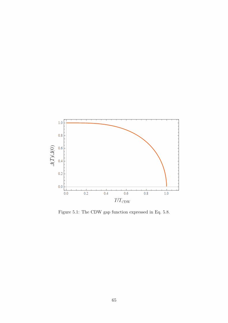
Figure 5.1: The CDW gap function expressed in Eq. 5.8.
65
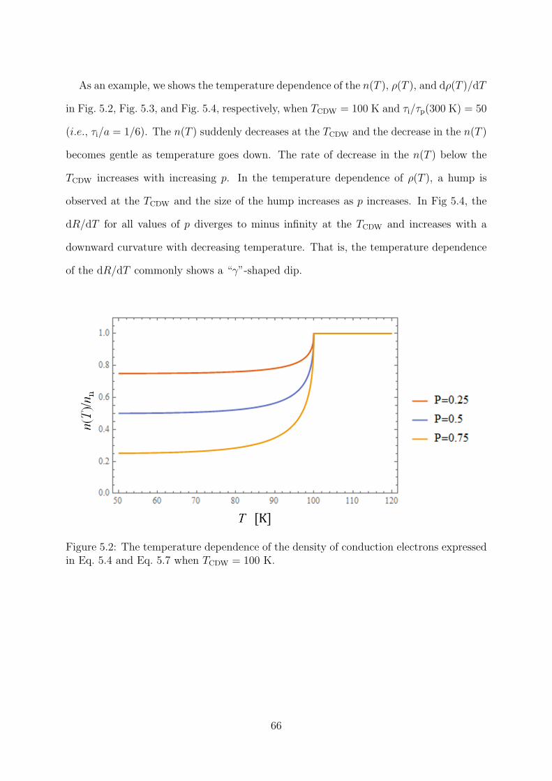
As an example, we shows the temperature dependence of the n(T ), ρ(T ), and dρ(T )/dT
in Fig. 5.2, Fig. 5.3, and Fig. 5.4, respectively, when TCDW = 100 K and τi/τp(300 K) = 50
(i.e., τi/a = 1/6). The n(T ) suddenly decreases at the TCDW and the decrease in the n(T )
becomes gentle as temperature goes down. The rate of decrease in the n(T ) below the
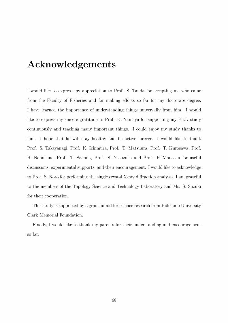
TCDW increases with increasing p. In the temperature dependence of ρ(T ), a hump is
observed at the TCDW and the size of the hump increases as p increases. In Fig 5.4, the
dR/dT for all values of p diverges to minus infinity at the TCDW and increases with a
downward curvature with decreasing temperature. That is, the temperature dependence
of the dR/dT commonly shows a “γ”-shaped dip.
Figure 5.2: The temperature dependence of the density of conduction electrons expressedin Eq. 5.4 and Eq. 5.7 when TCDW = 100 K.
66
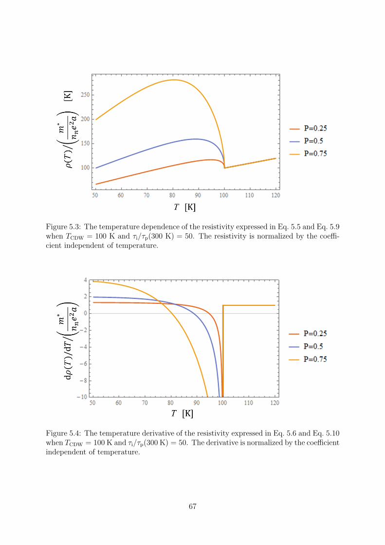
Figure 5.3: The temperature dependence of the resistivity expressed in Eq. 5.5 and Eq. 5.9when TCDW = 100 K and τi/τp(300 K) = 50. The resistivity is normalized by the coeffi-cient independent of temperature.
Figure 5.4: The temperature derivative of the resistivity expressed in Eq. 5.6 and Eq. 5.10when TCDW = 100 K and τi/τp(300 K) = 50. The derivative is normalized by the coefficientindependent of temperature.
67
Acknowledgements
I would like to express my appreciation to Prof. S. Tanda for accepting me who came
from the Faculty of Fisheries and for making efforts so far for my doctorate degree.
I have learned the importance of understanding things universally from him. I would
like to express my sincere gratitude to Prof. K. Yamaya for supporting my Ph.D study
continuously and teaching many important things. I could enjoy my study thanks to
him. I hope that he will stay healthy and be active forever. I would like to thank
Prof. S. Takayanagi, Prof. K. Ichimura, Prof. T. Matsuura, Prof. T. Kurosawa, Prof.
H. Nobukane, Prof. T. Sakoda, Prof. S. Yasuzuka and Prof. P. Monceau for useful
discussions, experimental supports, and their encouragement. I would like to acknowledge
to Prof. S. Noro for performing the single crystal X-ray diffraction analysis. I am grateful
to the members of the Topology Science and Technology Laboratory and Ms. S. Suzuki
for their cooperation.
This study is supported by a grant-in-aid for science research from Hokkaido University
Clark Memorial Foundation.
Finally, I would like to thank my parents for their understanding and encouragement
so far.
68
References
[1] J. G. Bednorz and K.A. Muller, Z. Phys. B - Condensed Matter 64, 189 (1986).
[2] L. Gao, Y. Y. Xue, F. Chen, Q. Xiong, R. L. Meng, D. Ramirez, C. W. Chu, J. H.
Eggert, and H. K. Mao, Phys. Rev. B 50, 4260(R) (1994).
[3] A. P. Drozdov, M. I. Eremets, I. A. Troyan, V. Ksenofontov, and S. I. Shylin, Nature
Phys. 525, 73 (2015).
[4] S. Yasuzuka, K. Murata, T. Fujimoto, M. Shimotori, and K. Yamaya, J. Phys. Soc.
Jpn. 74, 1782 (2005).
[5] E. Morosan, H. W. Zandbergen, B. S. Dennis, J. W. G. Bos, Y. Onose, T. Klimczuk,
A. P. Ramirez, N. P. Ong, and R. J. Cava, Nat. Phys. 2, 544 (2006).
[6] A. F. Kusmartseva, B. Sipos, H. Berger, L. Forro, and E. Tutis, Phys. Rev. Lett.
103, 236401 (2009).
[7] B. Sipos, A. F. Kusmartseva, A. Akrap, H. Berger, L. Forro, and E. Tutis, Nature
Mater. 7, 960 (2008).
[8] L. J. Li, W. J. Lu, X. D. Zhu, L. S. Ling, Z. Qu, and Y. P. Sun, Europhys. Lett.
97, 67005 (2012).
[9] X. Zhu, W. Ning, L. Li, L. Ling, R. Zhang, J. Zhang, K. Wang, Y. Liu, L. Pi, Y.
Ma, H. Du, M. Tian, Y. Sun, C. Petrovic, and Y. Zhang, Sci. Rep. 6, 26974 (2016).
[10] P. Monceau, Advances in Physics. 61, 325 (2012).
[11] P. Monceau, Physica B. 460, 2 (2015).
[12] T. Valla, A. V. Fedorov, P. D. Johnson, P-A. Glans, C. McGuinness, K. E. Smith,
E. Y. Andrei, and H. Berger, Phys. Rev. Lett. 92, 086401 (2004).
69
[13] K. Sugawara, Y. Nakata, R. Shimizu, P. Han, T. Hitosugi, T. Sato, and T. Taka-
hashi, ACS Nano. 10, 1341 (2016).
[14] R. Yomo, K. Yamaya, M. Abliz, M. Hedo and Y. Uwatoko, Phys. Rev. B 71,
132508 (2005).
[15] K. Kawabata, J. Phys. Soc. Jpn. 54, 762 (1985).
[16] A. M. Novello, M. Spera, A. Scarfato, A. Ubaldini, E. Giannini, D. R. Bowler, and
Ch. Renner, Phys. Rev. Lett. 118, 017002 (2017).
[17] A. Kogar, G. A. de la Pena, Sangjun Lee, Y. Fang, S. X. -L. Sun, D. B. Lioi, G.
Karapetrov, K. D. Finkelstein, J. P. C. Ruff, P. Abbamonte, and S. Rosenkranz,
Phys. Rev. Lett. 118, 027002 (2017).
[18] E. Bjerkelund and A. Kjekshus, Acta Chem. Scand. 19, 701 (1965).
[19] E. Bjerkelund, J. H. Fermor, and A. Kjekshus, Acta Chem. Scand. 20, 1836 (1966).
[20] A. Meerschaut and J. Rouxel, J. Less Common Metals 39, 197 (1975).
[21] J. Rijnsdorp and F. Jellinek, J. Solid State Chem. 25, 325 (1978).
[22] M. Yamamoto, J. Phys. Soc. Jpn. 45, 431 (1978).
[23] E. Canadell, I. E. -I. Rachidi, J. P. Pouget, P. Gressier, A. Meerschaut, J. Rouxel,
D. Jung, M. Evain, and M. -H. Whangbo, Inorg. Chem. 29, 1401 (1990).
[24] N. P. Ong and P. Monceau, Phys. Rev. B 16, 3443 (1977).
[25] T. Sambongi, K. Tsutsumi, Y. Shiozaki, M. Yamamoto, K. Yamaya, and Y. Abe,
Solid State Commun. 22, 729 (1977).
[26] Z. Z. Wang, P. Monceau, H. Salva, C. Roucau, L. Guemas, and A. Meerschaut,
Phys. Rev. B 40, 11589 (1989).
70
[27] T. Sambongi, M. Yamamoto, K. Tsutsumi, Y. Shiozaki, K. Yamaya, and Y. Abe,
J. Phys. Soc. Jpn. 42, 1421 (1977).
[28] H. P. Geserich, G. Scheiber, F. Levy, and P. Monceau, Physica B 143, 174 (1986).
[29] T. Takoshima, M. Ido, K. Tsutsumi, T. Sambongi, S. Honma, K. Yamaya, and Y.
Abe, Solid State Commun. 35, 911 (1980).
[30] N. P. Ong and J. W. Brill, Phys. Rev. B 18, 5265 (1978).
[31] A. Perucchi, C. Søndergaard, S. Mitrovic, M. Grioni, N. Barisic, H. Berger, L. Forro,
and L. Degiorgi, Eur. Phys. J. B 39, 433 (2004).
[32] M. N. Regueiro, Solid State Commun. 60, 797 (1986).
[33] T. Sambongi, M. Yamamoto, K. Tsutsumi, Y. Shiozaki, K. Yamaya, and Y. Abe,
J. Phys. Soc. Jpn. 42, 1421 (1977).
[34] K. Yamaya and G. Oomi, J. Phys. Soc. Jpn. 51, 3512 (1982).
[35] T. M. Tritt, E. P. Stillwell, and M. J. Skove, Phys. Rev. B 34, 6799 (1986).
[36] T. Tsuneta, Ph. D. thesis, Hokkaido University, 2004.
[37] A. A. Sinchenko, P. Lejay, and P. Monceau, Phys. Rev. B 85, 241104(R) (2012).
[38] J. Li, J. Peng, S. Zhang, and G. Chen, Phys. Rev. B 96, 174510 (2017).
[39] S. Takahashi, T. Sambongi, J. W. Brill, and W. Roark, Solid State Commun. 49,
1031 (1984).
[40] T. M. Rice and G. K. Scott, Phys. Rev. Lett. 35, 120 (1975).
[41] M. Morita and K. Yamaya, Jpn. J. Appl. Phys. 26, 975 (1987).
[42] S. Nagata, S. Ebisu, T. Aochi, Y. Kinoshita, S. Chikazawa, and K. Yamaya, J. Phys.
Chem. Solids. 52, 761 (1991).
71
[43] P. Haen, F. Lapierre, P. Monceau, M. Nunez Regueiro and J. Richard, Solid State
Commun. 26, 725 (1978).
[44] D. Bucheli, S. Caprara, C. Castellani and M. Grilli, New J. Phys. 15, 023014 (2013).
[45] S. Caprara, J. Biscaras, N. Bergeal, D. Bucheli, S. Hurand, C. Feuillet-Palma, A.
Rastogi, R. C. Budhani, J. Lesueur and M. Grilli, Phys. Rev. B 88, 020504(R)
(2013).
[46] G. E. D. K. Prawiroatmodjo, F. Trier, D. V. Christensen, Y. Chen, N. Pryds and
T. S. Jespersen, Phys. Rev. B 93, 184504 (2016).
[47] L. A. Turkevich and R. A. Klemm, Phys. Rev. B 19, 2520 (1979).
[48] S. Kagoshima, H. Nagasawa, and T. Sambongi, One-Dimensional Conductors
(Springer-Verlag, Berlin Heidelberg, 1988).
[49] J. M. Tranquada, B. J. Sternlieb, J. D. Axe, Y. Nakamura, and S. Uchida, Nature
375, 561 (1995).
72