Embed Size (px)
Citation preview
1. 서 론
최근 고효율 저가 박막형 태양전지 동향에 따라 칼코게나이
드(chalcogenide)계 태양전지가 주목받고 있다. 대표적인 칼코
게나이드계 태양전지로는 CIGS (copper indium gallium selenide)
및 CdTe (cadmium telluride) 기반의 박막 태양전지가 있으며,
현재까지 보고된 CIGS와 CdTe를 기반으로 하는 태양전지 소자
의 최고 전력변환효율(power conversion efficiency, PCE)은 각
각 22.9% (CIGS)와 21.0% (CdTe)이다1). 하지만 4성 분계(four
component system) 이상의 복잡한 물질로 구성되는 CIGS의 경
우 화학량론(stoichiometry) 조성에 대한 제어의 어려움이 있고,
인듐(indium, In)과 갈륨(gallium, Ga) 원소에 대한 매장량 한계
및 카드뮴(cadmium, Cd)과 셀레늄(selenium, Se)의 독성(toxicity)
은 개선되어야 할 문제로 지적되고 있다. 이러한 관점에서 풍부
한 자원량(earth-abundant)과 무독성(non-toxic) 특징을 갖는 친
환경(eco-friendly) 칼코게나이드 소재를 화합물 반도체 태양전
지(compound semiconductor solar cell)의 광 흡수층(light absorp-
tion layer)으로 응용하는 연구가 활발히 진행 중이다2,3). 친환경
칼코게나이드 소재 중에서 황화주석(tin sulfide, SnS)은 IV-VI
족 화합물 반도체 소재이며, 사방정계(orthorhombic) 결정구조와
1.1~1.4 eV의 밴드 갭 에너지(band gap energy), 1015~1018 cm3
범위를 가지는 캐리어 농도(carrier concentration, p), 그리고 104
cm-1 이상의 높은 흡수 계수(absorption coefficient, α)를 갖는 특
성으로 인해 태양전지의 흡수층으로 적용할 경우 대략 30% 정도
의 이론적 PCE를 갖는 것으로 알려져 있다4-7).
일반적으로 SnS 박막은 분무 열분해법(spray pyrolysis deposi-
tion, SPD)2), 화학 기상 증착법(chemical vapor deposition, CVD)8),
원자층 증착법(atomic layer deposition, ALD)9), 열 증착법(thermal
evaporation)10), 그리고 RF (radio frequency) 마그네트론 스퍼
터링(magnetron sputtering)11-17) 방법 등의 다양한 공정으로 제
조된다.
Current Photovoltaic Research 8(1) 33-38 (2020) pISSN 2288-3274
DOI:https://doi.org/10.21218/CPR.2020.8.1.033 eISSN 2508-125X
RF 마그네트론 스퍼터링법으로 성장 된 SnS 박막의 구조적 및 광학적
특성에 대한 증착 압력의 영향손승익1)ㆍ이상운1)ㆍ손창식2)ㆍ황동현2)*
1)재료공학과, 부산대학교, 부산, 462412)신소재공학부, 신라대학교, 부산, 46958
Influence of Deposition Pressure on Structural and Optical
Properties of SnS Thin Films Grown by RF Magnetron SputteringSeung-Ik Son1) ․ Sang Woon Lee1) ․ Chang Sik Son2) ․ Donghyun Hwang2)*1)School of Materials Science and Engineering, Pusan National University, Busan 46241, Korea
2)Division of Materials Science and Engineering, Silla University, Busan 46958, Korea
Received January 15, 2020; Revised February 6, 2020; Accepted February 7, 2020
ABSTRACT: Single-phased SnS thin films have been prepared by RF magnetron sputtering at various deposition pressures. The effect
of deposition pressure on the structural and optical properties of polycrystalline SnS thin films was studied using X-ray diffraction (XRD),
field-emission scanning electron microscopy (FE-SEM), X-ray photoelectron spectroscopy (XPS) and ultraviolet-visible-near infrared
(UV-Vis-NIR) spectrophotometer. The XRD analysis revealed the orthorhombic structure of the SnS thin films oriented along the (111)
plane direction. As the deposition pressure was increased from 5 mTorr to 15 mTorr, the intensity of the peak on the (111) plane increased,
and the intensity decreased under the condition of 20 mTorr. The binding energy difference at the Sn 3d5/2 and S 2p3/2 core levels was
about 324.5 eV, indicating that the SnS thin film was prepared as a pure Sn-S phase. The optical properties of the SnS thin films indicate
the presence of direct allowed transitions with corresponding energy band gap in the rang 1.47-1.57 eV.
Key words: SnS film, RF magnetron sputtering, Deposition pressure, Absorber layer, Solar cell
*Corresponding author: [email protected]
ⓒ 2020 by Korea Photovoltaic Society
This is an Open Access article distributed under the terms of the Creative Commons Attribution Non-Commercial License
(http://creativecommons.org/licenses/by-nc/3.0)
which permits unrestricted non-commercial use, distribution, and reproduction in any medium, provided the original work is properly cited.
33
S.I. Son et al. / Current Photovoltaic Research 8(1) 33-38 (2020)34
지금까지 보고된 바에 따르면, ALD 방법으로 제조한 SnS 박
막을 흡수층으로 적용한 태양전지의 효율(PCE)이 가장 높은
4.63% (2014년)를 기록하였다9). 그러나 ALD 공정의 매우 낮은
박막 증착 속도는 개선되어야 할 문제점으로 지적된다10). ALD
방법과 비교하여 스퍼터링 방법은 높은 증착 속도를 가짐으로
써 박막 제조 공정의 시간을 현저히 낮출 수 있다. 이에 덧붙여,
기판 온도와 스퍼터링 파워 및 증착 압력과 같은 여러 공정 변수
의 제어가 용이하고11-13), 균일한 물성을 가진 박막 구현과 조성
제어가 쉬운 이점이 있다18-21). 하지만 주석(Sn) 타깃과 황화수
소(H2S) 가스의 화학적 반응을 이용한 반응성 스퍼터링(reactive
sputtering) 방법으로 제조한 SnS 박막 태양전지의 효율은 0.26%
(2015년)15), 그리고 단일(single) SnS 스퍼터링 타깃과 RF 마그
네트론 스퍼터링 공정을 적용한 SnS 박막 태양전지의 효율은
0.38% (2019년)17)에 불과하다. 스퍼터링 공정으로 제조한 SnS-
흡수층 기반 태양전지의 낮은 효율은 고품질 SnS 박막 성장에
대한 증착 기술의 부재에서 찾을 수 있다.
본 연구에서는 SnS 박막을 단일 SnS 타깃을 사용한 RF 마그
네트론 스퍼터링 법으로 유리기판 상에 제조하였고, 증착 압력
의 변화에 따른 구조적 및 광학적 특성을 알아보았다.
2. 실험방법
RF 마그네트론 스퍼터링 법으로 25 × 25 mm2 크기의 소다석
회유리(Soda-lime glass, SLG) 기판 위에 SnS 박막을 성장시켰
다. 유리기판의 절단 과정에서 발생하는 미세 입자와 표면 불순
물을 제거하기 위하여 증류수(deionized water), 아세톤(acetone),
에탄올(ethanol), 그리고 아이소프로필알코올(isopropyl alcohol)
순으로 각각 5분간 초음파세척을 진행하였다. 초음파세척이 완
료된 기판 표면을 질소(N2) 가스총으로 완전히 건조한 후, 자외
선-오존 세정기(UV ozone cleaner)에 20분간 장입하여 잔류 유
기물을 제거하였다. SnS 단일 타깃(2 inch, 4N, TASCO)은 기판
으로부터 100 mm 거리를 유지한 채 아래 방향으로 장착하였고,
터보 분자 펌프(turbo molecular pump, TMP)를 사용하여 체임
버(chamber)의 초기 진공 압력을 3.3×10⁻⁶ Torr 미만으로 배기
하였다. SnS 박막 제조에 관한 세부 공정 조건을 Table 1에 나타
내었다.
SnS 박막의 결정구조를 X-선 회절 분석법(X-ray diffracto-
meter, XRD, Rigaku, Ultima IV)으로 확인하였고, SnS 박막의
표면 형상과 두께는 전계 방사형 주사전자현미경(field-emission
scanning electron microscopy, FE-SEM, TESCAN, MIRA 3)
으로 관찰하였다. 표면저항은 4-탐침 면저항측정기(4-point probe
system, CMT-SR2000N)로 측정하였다. SnS 박막의 화학량론
및 원자가 상태(valence state)는 X-선 광전자 분광법(X-ray photo-
electron spectroscopy, XPS, Thermo Scientific, K-Alpha+)으로
분석하였다.
SnS 박막의 광학적 특성은 600 nm에서 2000 nm의 파장 범위를
갖는 자외선-가시광선-근적외선(ultraviolet-visible-near infrared,
UV-Vis-NIR) 분광 광도계(spectrophotometer, JASCO, V-570)
를 사용하여 측정하였고, 측정된 흡수 계수(absorption coeffi-
cient, α)를 사용하여 SnS 박막의 밴드 갭 에너지를 평가하였다.
3. 결과 및 고찰
3.1 SnS 박막의 구조적 특성
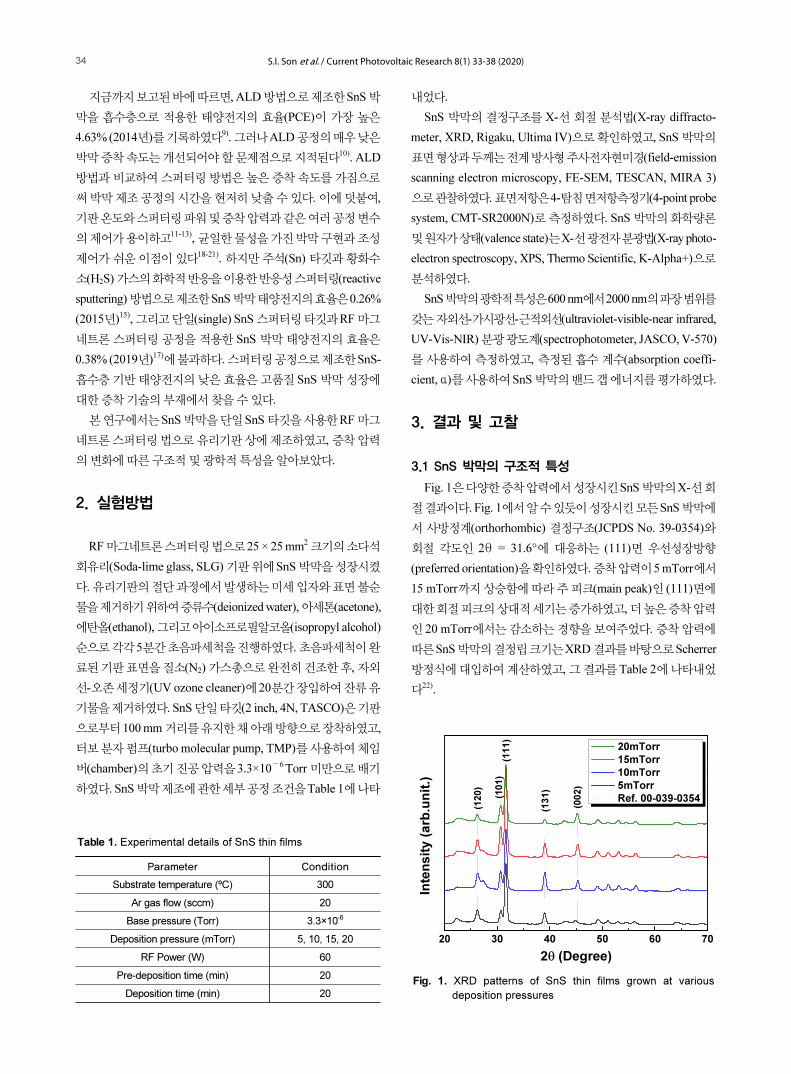
Fig. 1은 다양한 증착 압력에서 성장시킨 SnS 박막의 X-선 회
절 결과이다. Fig. 1에서 알 수 있듯이 성장시킨 모든 SnS 박막에
서 사방정계(orthorhombic) 결정구조(JCPDS No. 39-0354)와
회절 각도인 2θ = 31.6°에 대응하는 (111)면 우선성장방향
(preferred orientation)을 확인하였다. 증착 압력이 5 mTorr에서
15 mTorr까지 상승함에 따라 주 피크(main peak)인 (111)면에
대한 회절 피크의 상대적 세기는 증가하였고, 더 높은 증착 압력
인 20 mTorr에서는 감소하는 경향을 보여주었다. 증착 압력에
따른 SnS 박막의 결정립 크기는 XRD 결과를 바탕으로 Scherrer
방정식에 대입하여 계산하였고, 그 결과를 Table 2에 나타내었
다22).
Table 1. Experimental details of SnS thin films
Parameter Condition
Substrate temperature (ºC) 300
Ar gas flow (sccm) 20
Base pressure (Torr) 3.3×10⁻⁶
Deposition pressure (mTorr) 5, 10, 15, 20
RF Power (W) 60
Pre-deposition time (min) 20
Deposition time (min) 20
20 30 40 50 60 70
20mTorr
15mTorr
10mTorr
5mTorr
Ref. 00-039-0354
(131)
(002)
(101)
(120)
Inte
ns
ity
(arb
.un
it.)
2 (Degree)
(111)
Fig. 1. XRD patterns of SnS thin films grown at various
deposition pressures
S.I. Son et al. / Current Photovoltaic Research 8(1) 33-38 (2020) 35
5 mTorr에서 15 mTorr로 증착 압력이 높아짐에 따라 (111)면
에 대한 결정립의 크기는 20.2 nm에서 22.2 nm로 증가하였고,
20 mTorr에서는 20.8 nm로 그 크기가 감소하였다. (111)면에 대
한 주 피크의 강도 및 결정립 크기의 감소는 증착 압력이 증가할
수록 특정 압력에서 타깃에 충돌하는 아르곤(argon, Ar) 양이온
의 밀도(density)가 높아지고, 스퍼터링 된 원자와 이온 간의 상
호 간섭 빈도가 증가하여 핵 생성 및 핵 성장 과정에 부정적 영향
을 미치기 때문이다. 이와 유사한 현상을 스퍼터링 방법으로 성
장시킨 CIGS 박막의 연구 사례에서 찾을 수 있다21).
기판 온도(Ts)를 300°C로 고정하고, 공정 압력 변화(Pd = 5,
10, 15, 20 mTorr)시켜 증착한 SnS 박막의 표면 형상과 단면 및
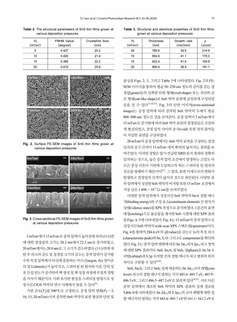
물성을 Figs. 2, 3, 그리고 Table 3에 나타내었다. Fig. 2의 FE-
SEM 이미지를 통하여 평균 50~250 nm 정도의 길이를 갖는 결
정립(grain)들의 길쭉한 타원 형태(oval-shape) 또는 귀리와 같
은 형태(oat-like shape)로 SnS 박막 표면에 균일하게 구성되었
음을 알 수 있다13,18,23). Fig. 3의 단면 이미지(cross-sectional
image)는 공정 압력에 따라 증착된 SnS 박막의 두께가 평균
800~900 nm 정도인 것을 보여준다. 공정 압력이 5 mTorr에서
15 mTorr로 증가함에 따라 SnS 박막 표면의 결정립들은 조밀하
게 형성되었고, 결정 입자 사이의 공극(void) 또한 점차 줄어들
어 치밀한 표면을 구성하였다.
20 mTorr의 공정 압력에서는 SnS 박막 표면을 구성하는 결정
입자의 공극 간격이 15 mTorr 대비 확연히 넓어지는 결과를 보
여주었다. 이러한 경향은 앞서 언급한 XRD 분석 결과와 정확히
일치하는 것으로, 높은 증착 압력 조건에서 발생하는 고밀도 아
르곤 중성 이온이 기판에 도달하고자 하는 스퍼터링 된 원자의
진로를 방해하기 때문이다21). 그 결과, 표면 미세구조의 변화가
발생하고 결정립의 간격이 넓어진 것으로 판단된다. 다양한 증
착 압력에서 성장한 SnS 박막의 비저항 또한 15 mTorr 조건에서
가장 낮은 1.698 × 10⁻² Ω·cm를 보여주었다.
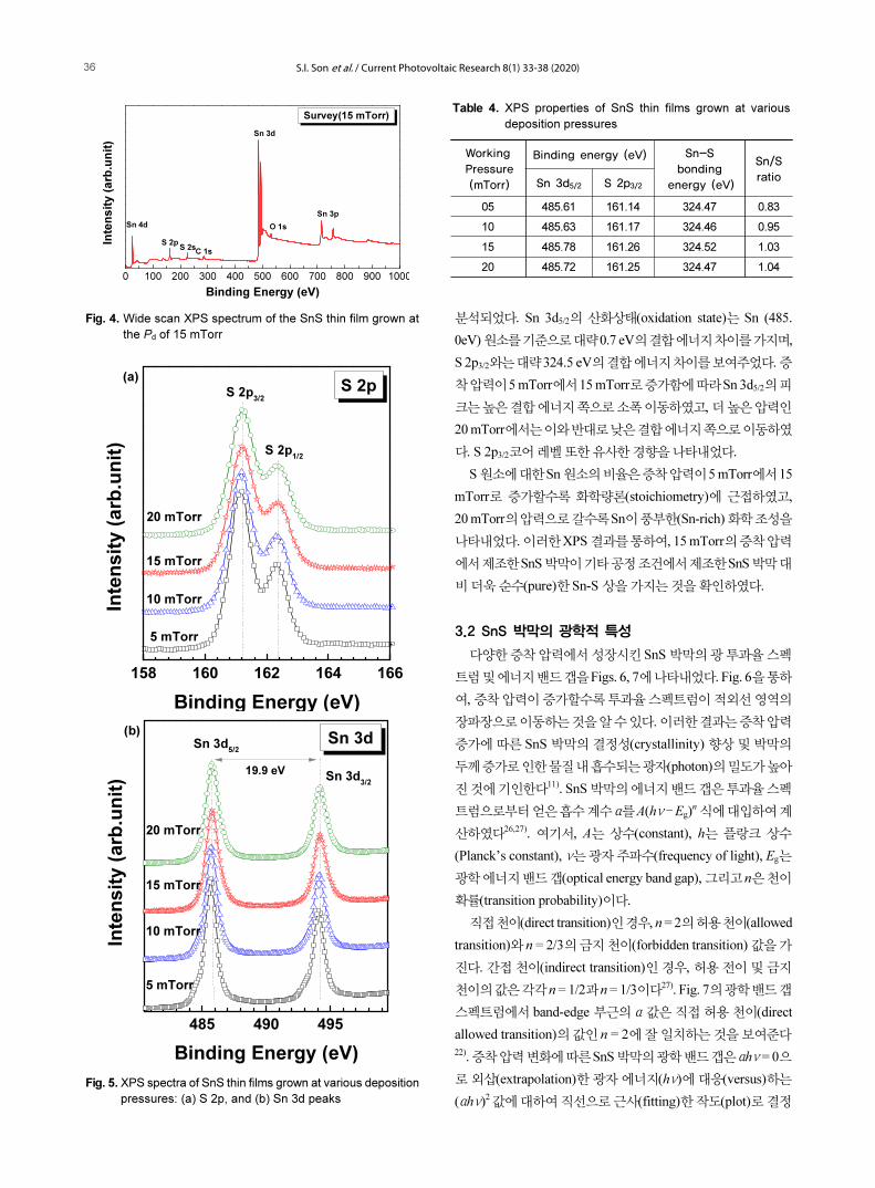
다양한 증착 압력에서 성장시킨 SnS 박막의 Sn-S 결합 에너
지(binding energy)와 구성 요소(constituent element) 간 원자가
상태(valence state)를 XPS 측정으로 분석하였다. 1분간의 표면
에칭(etching)으로 불순물을 제거한 SnS 시편에 대한 XPS 결과
를 Figs. 4, 5에 나타내었다. Fig. 4는 15 mTorr의 증착 압력으로
성장시킨 SnS 박막의 wide scan XPS 스펙트럼(spectrum)이다.
Fig. 4를 통하여 284.6 eV의 값(value)을 갖는 C 1s의 특성 피크
(characteristic peak)와 Sn, S, O 그리고 C components를 확인하
였다. Fig. 5는 증착 압력 변화에 따른 Sn 3d5/2와 S 2p3/2피크 영역
에 대한 XPS 결과이다. SnS, Sn2S3 및 SnS2 상(phase)은 Sn 3d 오
비탈(orbital)과 S 2p 오비탈 간의 결합 에너지 피크 범위의 위치
차이로 구분할 수 있다4,24).
SnS, Sn2S3 그리고 SnS2 상에 대응하는 Sn 3d5/2코어 레벨(core
level) 피크의 결합 에너지 범위는 각각 485.6~485.7 eV, 485.9~
486.5 eV, 그리고 486.5~487.3 eV로 알려져 있다24,25). 서로 다른
증착 압력에서 제조한 SnS 박막의 XPS 결과의 상세 정보를
Table 4에 나타내었다. Sn 3d5/2와 S 2p3/2의 코어 레벨에 대한 결
합 에너지의 범위는 각각 485.6~485.7 eV와 161.1~161.2 eV로
Table 2. The structural parameters of SnS thin films grown at
various deposition pressures
Pd
(mTorr)
FWHM Value
(degree)
Crystallite Size
(nm)
5 0.427 20.2
10 0.420 21.4
15 0.389 22.2
20 0.415 20.8
Fig. 2. Surface FE-SEM images of SnS thin films grown at
various deposition pressures
Fig. 3. Cross-sectional FE-SEM images of SnS thin films grown
at various deposition pressures
Table 3. Structural and electrical properties of SnS thin films
grown at various deposition pressures
Pd
(mTorr)
Thickness
(nm)
Growth rate
(nm/min)
ρ
(Ωcm)
05 780.6 39.5 214.9
10 854.9 41.1 170.3
15 922.4 41.6 169.8
20 890.9 38.9 181.1
S.I. Son et al. / Current Photovoltaic Research 8(1) 33-38 (2020)36
분석되었다. Sn 3d5/2의 산화상태(oxidation state)는 Sn (485.
0eV) 원소를 기준으로 대략 0.7 eV의 결합 에너지 차이를 가지며,
S 2p3/2와는 대략 324.5 eV의 결합 에너지 차이를 보여주었다. 증
착 압력이 5 mTorr에서 15 mTorr로 증가함에 따라 Sn 3d5/2의 피
크는 높은 결합 에너지 쪽으로 소폭 이동하였고, 더 높은 압력인
20 mTorr에서는 이와 반대로 낮은 결합 에너지 쪽으로 이동하였
다. S 2p3/2코어 레벨 또한 유사한 경향을 나타내었다.
S 원소에 대한 Sn 원소의 비율은 증착 압력이 5 mTorr에서 15
mTorr로 증가할수록 화학량론(stoichiometry)에 근접하였고,
20 mTorr의 압력으로 갈수록 Sn이 풍부한(Sn-rich) 화학 조성을
나타내었다. 이러한 XPS 결과를 통하여, 15 mTorr의 증착 압력
에서 제조한 SnS 박막이 기타 공정 조건에서 제조한 SnS 박막 대
비 더욱 순수(pure)한 Sn-S 상을 가지는 것을 확인하였다.
3.2 SnS 박막의 광학적 특성
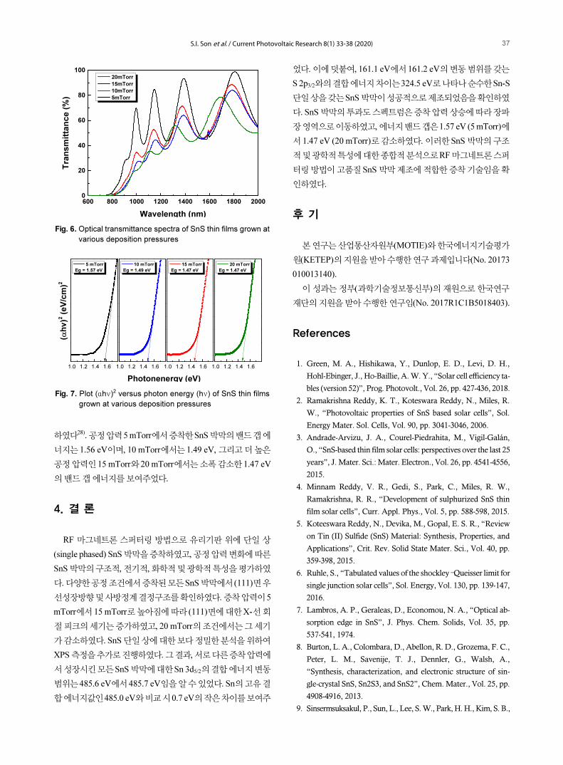
다양한 증착 압력에서 성장시킨 SnS 박막의 광 투과율 스펙
트럼 및 에너지 밴드 갭을 Figs. 6, 7에 나타내었다. Fig. 6을 통하
여, 증착 압력이 증가할수록 투과율 스펙트럼이 적외선 영역의
장파장으로 이동하는 것을 알 수 있다. 이러한 결과는 증착 압력
증가에 따른 SnS 박막의 결정성(crystallinity) 향상 및 박막의
두께 증가로 인한 물질 내 흡수되는 광자(photon)의 밀도가 높아
진 것에 기인한다11). SnS 박막의 에너지 밴드 갭은 투과율 스펙
트럼으로부터 얻은 흡수 계수 α를 A(hν – Eg)n 식에 대입하여 계
산하였다26,27). 여기서, A는 상수(constant), h는 플랑크 상수
(Planck’s constant), ν는 광자 주파수(frequency of light), Eg는
광학 에너지 밴드 갭(optical energy band gap), 그리고 n은 천이
확률(transition probability)이다.
직접 천이(direct transition)인 경우, n = 2의 허용 천이(allowed
transition)와 n = 2/3의 금지 천이(forbidden transition) 값을 가
진다. 간접 천이(indirect transition)인 경우, 허용 전이 및 금지
천이의 값은 각각 n = 1/2과 n = 1/3이다27). Fig. 7의 광학 밴드 갭
스펙트럼에서 band-edge 부근의 α 값은 직접 허용 천이(direct
allowed transition)의 값인 n = 2에 잘 일치하는 것을 보여준다22). 증착 압력 변화에 따른 SnS 박막의 광학 밴드 갭은 αhν = 0으
로 외삽(extrapolation)한 광자 에너지(hν)에 대응(versus)하는
(αhν)2 값에 대하여 직선으로 근사(fitting)한 작도(plot)로 결정
0 100 200 300 400 500 600 700 800 900 1000
S 2sC 1s
S 2p
Sn 4d
Sn 3p
O 1s
Survey(15 mTorr)
Binding Energy (eV)
Inte
ns
ity
(a
rb.u
nit
)
Sn 3d
Fig. 4. Wide scan XPS spectrum of the SnS thin film grown at
the Pd of 15 mTorr
158 160 162 164 166
(a)
S 2p1/2
S 2p3/2
Inte
ns
ity
(a
rb.u
nit
)
Binding Energy (eV)
S 2p
20 mTorr
15 mTorr
10 mTorr
5 mTorr
485 490 495
(b)
19.9 eVSn 3d
3/2
Sn 3d5/2
Sn 3d
20 mTorr
15 mTorr
10 mTorr
Inte
nsit
y (
arb
.un
it)
Binding Energy (eV)
5 mTorr
Fig. 5. XPS spectra of SnS thin films grown at various deposition
pressures: (a) S 2p, and (b) Sn 3d peaks
Table 4. XPS properties of SnS thin films grown at various
deposition pressures
Working
Pressure
(mTorr)
Binding energy (eV) Sn-S
bonding
energy (eV)
Sn/S
ratioSn 3d5/2 S 2p3/2
05 485.61 161.14 324.47 0.83
10 485.63 161.17 324.46 0.95
15 485.78 161.26 324.52 1.03
20 485.72 161.25 324.47 1.04
S.I. Son et al. / Current Photovoltaic Research 8(1) 33-38 (2020) 37
하였다28). 공정 압력 5 mTorr에서 증착한 SnS 박막의 밴드 갭 에
너지는 1.56 eV이며, 10 mTorr에서는 1.49 eV, 그리고 더 높은
공정 압력인 15 mTorr와 20 mTorr에서는 소폭 감소한 1.47 eV
의 밴드 갭 에너지를 보여주었다.
4. 결 론
RF 마그네트론 스퍼터링 방법으로 유리기판 위에 단일 상
(single phased) SnS 박막을 증착하였고, 공정 압력 변화에 따른
SnS 박막의 구조적, 전기적, 화학적 및 광학적 특성을 평가하였
다. 다양한 공정 조건에서 증착된 모든 SnS 박막에서 (111)면 우
선성장방향 및 사방정계 결정구조를 확인하였다. 증착 압력이 5
mTorr에서 15 mTorr로 높아짐에 따라 (111)면에 대한 X-선 회
절 피크의 세기는 증가하였고, 20 mTorr의 조건에서는 그 세기
가 감소하였다. SnS 단일 상에 대한 보다 정밀한 분석을 위하여
XPS 측정을 추가로 진행하였다. 그 결과, 서로 다른 증착 압력에
서 성장시킨 모든 SnS 박막에 대한 Sn 3d5/2의 결합 에너지 변동
범위는 485.6 eV에서 485.7 eV임을 알 수 있었다. Sn의 고유 결
합 에너지값인 485.0 eV와 비교 시 0.7 eV의 작은 차이를 보여주
었다. 이에 덧붙여, 161.1 eV에서 161.2 eV의 변동 범위를 갖는
S 2p3/2와의 결합 에너지 차이는 324.5 eV로 나타나 순수한 Sn-S
단일 상을 갖는 SnS 박막이 성공적으로 제조되었음을 확인하였
다. SnS 박막의 투과도 스펙트럼은 증착 압력 상승에 따라 장파
장 영역으로 이동하였고, 에너지 밴드 갭은 1.57 eV (5 mTorr)에
서 1.47 eV (20 mTorr)로 감소하였다. 이러한 SnS 박막의 구조
적 및 광학적 특성에 대한 종합적 분석으로 RF 마그네트론 스퍼
터링 방법이 고품질 SnS 박막 제조에 적합한 증착 기술임을 확
인하였다.
후 기
본 연구는 산업통산자원부(MOTIE)와 한국에너지기술평가
원(KETEP)의 지원을 받아 수행한 연구 과제입니다(No. 20173
010013140).
이 성과는 정부(과학기술정보통신부)의 재원으로 한국연구
재단의 지원을 받아 수행한 연구임(No. 2017R1C1B5018403).
References
1. Green, M. A., Hishikawa, Y., Dunlop, E. D., Levi, D. H.,
Hohl-Ebinger, J., Ho-Baillie, A. W. Y., “Solar cell efficiency ta-
bles (version 52)”, Prog. Photovolt., Vol. 26, pp. 427-436, 2018.
2. Ramakrishna Reddy, K. T., Koteswara Reddy, N., Miles, R.
W., “Photovoltaic properties of SnS based solar cells”, Sol.
Energy Mater. Sol. Cells, Vol. 90, pp. 3041-3046, 2006.
3. Andrade-Arvizu, J. A., Courel-Piedrahita, M., Vigil-Galán,
O., “SnS-based thin film solar cells: perspectives over the last 25
years”, J. Mater. Sci.: Mater. Electron., Vol. 26, pp. 4541-4556,
2015.
4. Minnam Reddy, V. R., Gedi, S., Park, C., Miles, R. W.,
Ramakrishna, R. R., “Development of sulphurized SnS thin
film solar cells”, Curr. Appl. Phys., Vol. 5, pp. 588-598, 2015.
5. Koteeswara Reddy, N., Devika, M., Gopal, E. S. R., “Review
on Tin (II) Sulfide (SnS) Material: Synthesis, Properties, and
Applications”, Crit. Rev. Solid State Mater. Sci., Vol. 40, pp.
359-398, 2015.
6. Ruhle, S., “Tabulated values of the shockley –Queisser limit for
single junction solar cells”, Sol. Energy, Vol. 130, pp. 139-147,
2016.
7. Lambros, A. P., Geraleas, D., Economou, N. A., “Optical ab-
sorption edge in SnS”, J. Phys. Chem. Solids, Vol. 35, pp.
537-541, 1974.
8. Burton, L. A., Colombara, D., Abellon, R. D., Grozema, F. C.,
Peter, L. M., Savenije, T. J., Dennler, G., Walsh, A.,
“Synthesis, characterization, and electronic structure of sin-
gle-crystal SnS, Sn2S3, and SnS2”, Chem. Mater., Vol. 25, pp.
4908-4916, 2013.
9. Sinsermsuksakul, P., Sun, L., Lee, S. W., Park, H. H., Kim, S. B.,
600 800 1000 1200 1400 1600 1800 2000
0
20
40
60
80
100
20mTorr
15mTorr
10mTorr
5mTorr
Tra
ns
mit
tan
ce
(%
)
Wavelength (nm)
Fig. 6. Optical transmittance spectra of SnS thin films grown at
various deposition pressures
1.0 1.2 1.4 1.6 1.0 1.2 1.4 1.6 1.0 1.2 1.4 1.6 1.0 1.2 1.4 1.6
5 mTorr
Eg = 1.57 eV
(h
v)2
(eV
/cm
)2
Photonenergy (eV)
10 mTorr
Eg = 1.49 eV
15 mTorr
Eg = 1.47 eV
20 mTorr
Eg = 1.47 eV
Fig. 7. Plot (αhν)2 versus photon energy (hν) of SnS thin films
grown at various deposition pressures
S.I. Son et al. / Current Photovoltaic Research 8(1) 33-38 (2020)38
Yang, C., Gordon, R. G., “Overcoming Efficiency Limitations
of SnS-Based Solar Cells”, Adv. Energy Mater., Vol. 4, p.
1400496, 2014.
10. Steinmann, V., Jaramillo, R., Hartman, K., Chakraborty, R.,
Brandt, R. E., Poindexter, J. R., Lee, Y. S., Sun, L., Polizzotti,
A., Park, H. H., Gordon, R. G., Buonassisi, T., “3.88% efficient
tin sulfide solar cells using congruent thermal evaporation”,
Adv. Mater., Vol. 26, pp. 7488-7492, 2014.
11. Banai, R. E., Lee, H., Motyka, M. A., Chandrasekharan, R.,
Podraza, N. J., Brownson, J. R. S., Horn, M. W., “Optical
properties of sputtered SnS thin films for photovoltaic absorb-
ers”, IEEE J. Photovolt., Vol. 3, pp. 1084-1089, 2013.
12. Sousa, M. G., Da Cunha, A. F., Fernandes, P. A., “Annealing
of RF-magnetron sputtered SnS2 precursors as a new route for
single phase SnS thin films”, J. Alloys Compd., Vol. 592, pp.
80-85, 2014.
13. Banai, R. E., Lee, H., Zlotnikov, S., Brownson, J. R. S., Horn,
M. W., “Phase identification of RF-sputtered SnS thin films us-
ing rietveld analysis of X-ray diffraction patterns”, 39th IEEE
Photovoltaic Specialists Conference, 2562-2566, 2013.
14. Malaquias, J., Fernandes, P. A., Salomé, P. M. P., Da Cunha,
A. F., “Assessment of the potential of tin sulphide thin films
prepared by sulphurization of metallic precursors as cell absorb-
ers”, Thin Solid Films, Vol. 519, pp. 7416-7420, 2011.
15. Zhao, L. B., Di, Y. X., Yan, C., Liu, F. Y., Cheng, Z., Jiang, L.
X., Hao, X. J., Lai, Y. Q., Li, J., “In situ growth of SnS absorb-
ing layer by reactive sputtering for thin film solar cells”, Rsc
Adv., Vol. 6, pp. 4108-4115, 2016.
16. Arepalli, V. K., Kim, J., “Effect of substrate temperature on the
structural and optical properties of radio frequency sputtered
tin sulfide thin films for solar cell application”, Thin Solid
Films, Vol. 666, pp. 34-39, 2018.
17. Arepalli, V. K., Shin, Y., Kim, J., “Photovoltaic behavior of the
room temperature grown RF-Sputtered SnS thin films”, Opt.
Mater., Vol. 88, pp. 594-600, 2019.
18. Hwang, D., “Structural and Optical Properties of SnS Thin
Films Deposited by RF Magnetron Sputtering”, Journal of the
Korean institute of surface engineering, Vol. 51, pp. 126-132,
2018.
19. Lokhande, A. C., Chalapathy, R. B. V., He, M., Jo, E., Gang,
M., Pawar, S. A., Lokhande, C. D., Kim, J. H., “Development
of Cu2SnS3 (CTS) thin film solar cells by physical techniques:
A status review”, Sol. Energ. Mat. Sol. C., Vol. 153, pp. 84-107,
2016.
20. Suryawanshi, M. P., Agawane, G. L., Bhosale, S. M., Shin, S.
W., Patil, P. S., Kim, J. H., Moholkar, A. V., “CZTS based thin
film solar cells: a status review”, Mater. Technol., Vol. 28, pp.
98-109, 2013.
21. Zhang, H. X., Hong, R. J., “CIGS absorbing layers prepared by
RF magnetron sputtering from a single quaternary target”,
Ceram. Int., Vol. 42, pp. 14543-14547, 2016.
22. Reddy, T. S., Kumar, M. C. S., “Co-evaporated SnS thin films
for visible light photodetector applications”, Rsc Adv., Vol. 6,
pp. 95680-95692, 2016.
23. Hartman, K., Johnson, J. L., Bertoni, M. I., Recht, D., Aziz,
M. J., Scarpulla, M. A., Buonassisi, T., “SnS thin-films by RF
sputtering at room temperature”, Thin Solid Films, Vol. 519,
pp. 7421-7424, 2011.
24. Gao, C., Shen, H. L., Sun, L., Huang, H. B., Lu, L. F., Cai, H.,
“Preparation of SnS films with zinc blende structure by succes-
sive ionic layer adsorption and reaction method”, Mater. Lett.,
Vol. 64, pp. 2177-2179, 2010.
25. Huang, C. C., Lin, Y. J., Chuang, C. Y., Liu, C. J., Yang, Y.
W., “Conduction-type control of SnSx films prepared by the
sol-gel method for different sulfur contents”, J. Alloy Compd.,
Vol. 553, pp. 208-211, 2013.
26. Chen, D., Shen, G. Z., Tang, K. B., Lei, S. J., Zheng, H. G.,
Qian, Y. T., “Microwave-assisted polyol synthesis of nanoscale
SnSx(x=1,2) flakes”, J. Cryst. Growth, Vol. 260, pp. 469-474,
2004.
27. Kawano, K., Nakata, R., Sumita, M., “Effects of Substrate-
Temperature on Absorption-Edge and Photocurrent in
Evaporated Amorphous SnS2 Films”, J. Phys. D. Appl. Phys.,
Vol. 22, pp. 136-141, 1989.
28. Sinsermsuksakul, P., Heo, J., Noh, W., Hock, A. S., Gordon,
R. G., “Atomic Layer Deposition of Tin Monosulfide Thin
Films”, Adv. Energy Mater., Vol. 1, pp. 1116-1125, 2011.
![Influence of Thickness on the Structural, Morphological and Optical Properties … · 2021. 4. 27. · shown the improved selectivity of nitrogen from water [22-27]. Various deposition](https://img.pdfslide.tips/doc/110x75/6138e6fba4cdb41a985b5b90/influence-of-thickness-on-the-structural-morphological-and-optical-properties-2021.jpg)


![High optical and structural quality of GaN epilayers grown ...projects.itn.pt/marco_fct/[4]High optical and structural quality of GaN... · High optical and structural quality of](https://img.pdfslide.tips/doc/110x75/5e880c2016bca472f2564feb/high-optical-and-structural-quality-of-gan-epilayers-grown-4high-optical-and.jpg)