Embed Size (px)
Citation preview
Instant Inkjet Circuits: Lab-based Inkjet Printing to SupportRapid Prototyping of UbiComp Devices
Yoshihiro KawaharaThe University of Tokyo
7-3-1 Hongo, Bunkyo-ku,Tokyo, Japan
Steve HodgesMicrosoft Research
CambridgeCambridge, United Kingdom
Benjamin S. CookGeorgia Institute of
TechnologyAtlanta, Georgia, U.S.A.
Cheng ZhangGeorgia Institute of
TechnologyAtlanta, Georgia, [email protected]
Gregory D. AbowdGeorgia Institute of
TechnologyAtlanta, Georgia, U.S.A.
ABSTRACTThis paper introduces a low cost, fast and accessible tech-nology to support the rapid prototyping of functional elec-tronic devices. Central to this approach of ‘instant inkjet cir-cuits’ is the ability to print highly conductive traces and pat-terns onto flexible substrates such as paper and plastic filmscheaply and quickly. In addition to providing an alternative tobreadboarding and conventional printed circuits, we demon-strate how this technique readily supports large area sensorsand high frequency applications such as antennas. Unlike ex-isting methods for printing conductive patterns, conductivityemerges within a few seconds without the need for specialequipment. We demonstrate that this technique is feasibleusing commodity inkjet printers and commercially availableink, for an initial investment of around US$300. Having pre-sented this exciting new technology, we explain the tools andtechniques we have found useful for the first time. Our mainresearch contribution is to characterize the performance of in-stant inkjet circuits and illustrate a range of possibilities thatare enabled by way of several example applications which wehave built. We believe that this technology will be of immedi-ate appeal to researchers in the ubiquitous computing domain,since it supports the fabrication of a variety of functional elec-tronic device prototypes.
Author KeywordsInkjet-printing; Conductive Ink; Capacitive Sensors; RapidPrototyping; Digital Fabrication.
ACM Classification KeywordsB.m. Hardware: Miscellaneous
Permission to make digital or hard copies of part or all of this work for personal orclassroom use is granted without fee provided that copies are not made or distributedfor profit or commercial advantage and that copies bear this notice and the full cita-tion on the first page. Copyrights for third-party components of this work must behonored. For all other uses, contact the owner/author(s). Copyright is held by the au-thor/owner(s).UbiComp’13, September 8–12, 2013, Zurich, Switzerland.ACM 978-1-4503-1770-2/13/09.http://dx.doi.org/10.1145/2493432.2493486
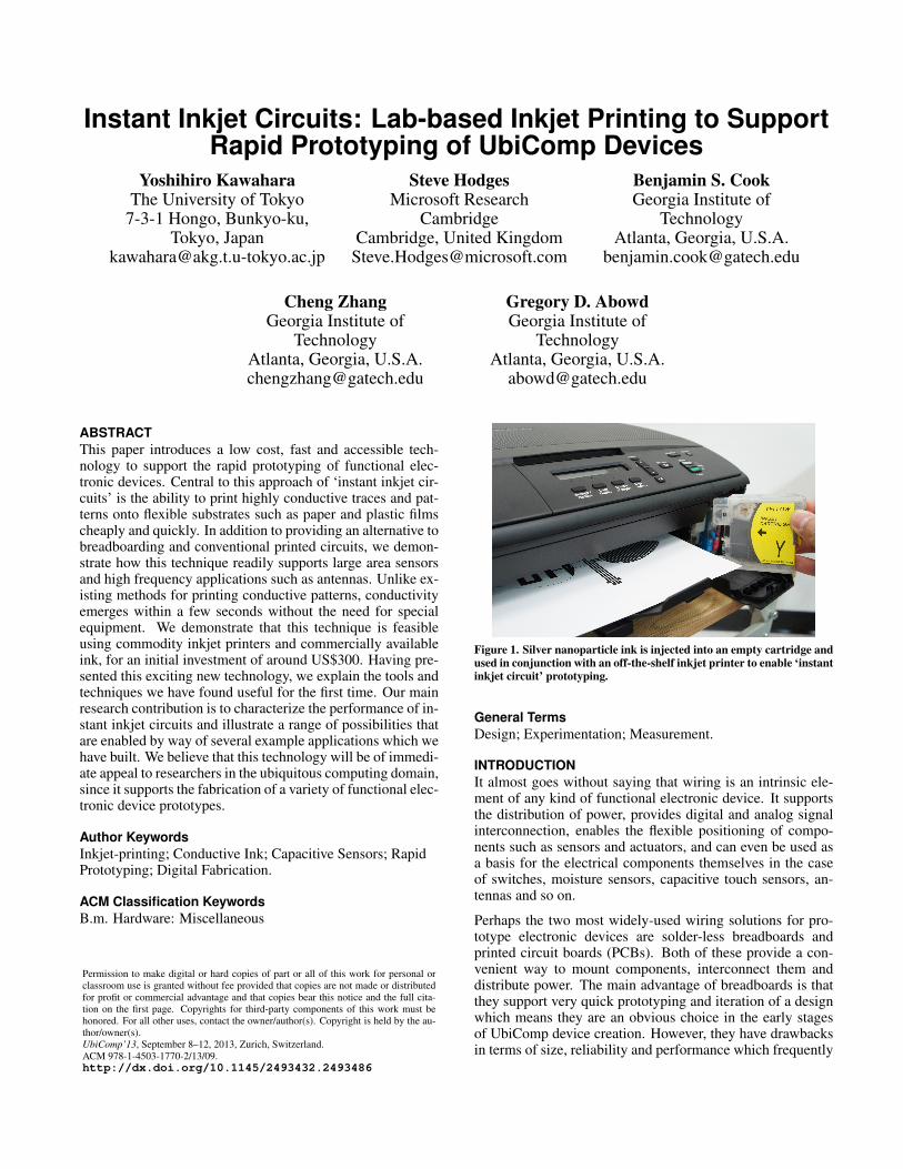
Figure 1. Silver nanoparticle ink is injected into an empty cartridge andused in conjunction with an off-the-shelf inkjet printer to enable ‘instantinkjet circuit’ prototyping.
General TermsDesign; Experimentation; Measurement.
INTRODUCTIONIt almost goes without saying that wiring is an intrinsic ele-ment of any kind of functional electronic device. It supportsthe distribution of power, provides digital and analog signalinterconnection, enables the flexible positioning of compo-nents such as sensors and actuators, and can even be used asa basis for the electrical components themselves in the caseof switches, moisture sensors, capacitive touch sensors, an-tennas and so on.
Perhaps the two most widely-used wiring solutions for pro-totype electronic devices are solder-less breadboards andprinted circuit boards (PCBs). Both of these provide a con-venient way to mount components, interconnect them anddistribute power. The main advantage of breadboards is thatthey support very quick prototyping and iteration of a designwhich means they are an obvious choice in the early stagesof UbiComp device creation. However, they have drawbacksin terms of size, reliability and performance which frequently
make a transition to a PCB prototype inevitable. The cus-tom nature of PCBs means that they are more versatile, cansupport physically smaller prototypes and are usually morerobust. They also support much higher fidelity design whichallows experimentation with conductive structures that havespecial sensing and/or radio frequency (RF) properties.
Whilst PCBs are well-suited to mass-production, they haveseveral disadvantages in a prototyping context. In particu-lar the time and cost involved in having them manufacturedis often at odds with the rapid iteration inherent in research.Online PCB production services have advanced a lot in recentyears, but sending a design away and waiting for a couple ofdays is still very different from making a board in the lab andtrying it out just hours later. Whilst some lab-based PCB fab-rication machines exist, they are not cheap, can be fiddly toset up and maintain, and as a result have only enjoyed lim-ited adoption to date. If a particular project requires a flexiblesubstrate (so called flex-PCBs) this is even more problematic,with simple prototypes often costing many hundreds of dol-lars to produce with turnaround times in excess of a week.And until now, producing flex-PCB prototypes in the lab hasnot really been feasible.
Our objective is to provide the means for researchers to printflexible circuits quickly, easily and cheaply, in a lab environ-ment. In this way we hope to introduce an intermediate alter-native to breadboards and custom PCBs which will have clearbenefits in certain UbiComp prototyping scenarios.
This paper describes our new solution for printing circuitswhich are flexible both in the physical sense and in terms ofthe applications which they support. Following a review ofrelated work in this area, we describe our ‘instant inkjet cir-cuit’ approach in some detail for the first time. We share thebest practices we have developed and characterize the resultswe have seen. We then present a number of applications forthis technology which we think will be of interest to otherresearchers in the broad field of ubiquitous computing. Weend by discussing a number of issues that have come to lightduring this research and future directions we would like topursue. Our ultimate aim is to empower and motivate othersto replicate, use and extend our work.
RELATED WORK
UbiComp research which motivates this workWhilst physical rapid prototyping tools such as laser cuttersand 3D printers have advanced tremendously in recent yearsand are now standard tools for UbiComp research, we feelthere is still an opportunity for equivalent advances in electri-cal rapid prototyping. Our work is inspired by a number ofinnovative ideas presented in the UbiComp-related researchliterature, where we feel that more powerful prototyping toolsfor electrical circuitry may have been valuable in facilitatingfaster and wider exploration. We start by reviewing someof these projects to illustrate these opportunities. We thenpresent the current state-of-the-art in tools and materials forquick electrical prototyping.
The domain of ‘digital crafting’ – manually constructing dig-ital artifacts from a range of less conventional materials to
create artistic and engaging functional devices – is becomingpopular. For example in Pulp-Based Computing [5], the au-thors present a way of embedding conductors and electroniccircuitry into a single sheet of hand-made paper. Other rele-vant projects from the literature include Kit-of-no-parts [16]and Electronic Popables [17]. We recognize that digital craft-ing is by its nature a quite manually intensive process, butnone-the-less we feel that an accessible electrical circuit pro-totyping tool would be a valuable extension to the crafter’stoolbox.
Midas is a tool which supports the design of customized con-ductive patterns for touch sensing applications, with the aimof making it easier to add interactivity to prototype devices[20]. Midas automatically generates layout files with the ap-propriate sensor pads and routed connections. The authorsdemonstrate two different ways of converting these layoutsinto physical prototypes, but also describe the limitations ofeach of these. They point to conductive inkjet printing as anideal solution, if it were more accessible to researchers.
In [10], Gong et al. propose the use of a relatively new roll-to-roll conductive inkjet printing process to build a scalable andversatile sensing surface for UbiComp applications. One ofthe contributions of this work was the use of relatively cheapfabrication of large-area printed circuits to distribute sensorsincluding printed antennas in the environment – in this caseunder the floor. In order to achieve acceptable performance interms of resolution and conductivity, the authors had to out-source fabrication, and even though a local company had theexpertise and equipment to support this, it was both expensiveand time-consuming.
Wimmer et al. propose a novel deformable touch-sensing sur-face using time domain reflectrometry [21]. This approachis unique in the sense that touch is detected as an impedancechange in a pair of conductive lines. Perhaps the biggest limi-tation of this approach is the cost and size of the time domainreflectometry equipment necessary to accurately distinguishsmall time difference of less than 50 ps, but another limitationis the form of the conductive lines; being able to print theseto suit a particular application would be an interesting con-cept. Tactile Tape is a flexible low-cost tape for touch sens-ing [12]. The tape consists of three layers (resistive, spacerand conductive) and functions as resistive one-dimensionalsingle-point touch sensor. Since it is fabricated using a metalsheet the design cannot be readily modified. Again, a tool forrapidly prototyping conductive circuits would facilitate this.
Other research explores the use of RFID tags for battery-lesssensing, for example detecting the level of liquid in a drink-ing glass [3] or detecting when an RFID tag (and the goodsit is tagging) has been subjected to temperatures outside anacceptable range [4]. In both of these examples the authorsreport that it would be beneficial to explore custom RFID tagantenna designs to further explore the design space and thepotential of their approaches.
As mentioned above, the aim of our work is to support sce-narios like these by providing an accessible, cheap and quick
method for printing arbitrarily-shaped conductors onto con-venient materials, both rigid and flexible.
On-demand fabrication tools for custom circuitsPCB milling machines such as the desktop LPKF ProMat S-Series [14] provide a reasonably accessible route to rapid-prototyping circuit boards in a lab setting. These machinesremove areas of copper from a copper-clad sheet of rigidPCB material to create pads, signal traces and conductivestructures. Compared with conventional fabrication methodsbased on a chemical etching process, PCB milling machinesare relatively fast and convenient. However, it still takes onthe order of an hour to set up and mill a board, maybe longerdepending on its size and complexity, and it is a relativelynoisy and messy process. Moreover, it is very difficult to millflexible substrates.
An alternative approach is the use of a commercial vinyl cut-ting machine – essentially a plotter with a cutting knife in-stead of a pen – in conjunction with adhesive-backed cop-per foil. Other UbiComp researchers have pointed out thatthis approach is relatively cheap (e.g. US$200 for the ma-chine, around US$10 per meter for the film). It is also ver-satile due to the high conductivity of copper and the physicalflexibility of the adhesive foil [20]. However, the subtractivenature of the process has several weaknesses: removing un-wanted material after the cutting is complete is tedious andtime-consuming, and thin traces can break when the materialaround them is removed [20].
A third alternative which is frequently used in industrial envi-ronments is inkjet printing. Based on recently developed sil-ver nanoparticle inks such as the Xerox ‘silver bullet’ [9] thistechnology supports great versatility in terms of the conduc-tive structures which can be created. This ‘additive’ approachto production is very attractive because it overcomes most ofthe disadvantages of the ‘subtractive’ milling and cutting pro-cesses described above. The main drawback of this fabrica-tion method is the price of the equipment. A highly special-ized inkjet printer is typically used, such as a FUJIFILM Di-matix DMP-2800 [8] which costs several tens of thousandsof dollars. Also, the printed ink is not initially conductive be-cause the silver nanoparticles have a polymer shell which pro-hibits agglomeration while in suspension. Once deposited,the ink must be sintered in an oven at more than 150 C forseveral hours in order to form mutual connections among themetal particles. Not only does this limit the substrates thatcan be used and require additional equipment, it also dramat-ically reduces the speed with which it is possible to produceprototypes.
Sintering-free Conductive Ink and PaintRecent advances in materials science have resulted in a va-riety of commercially-available conductive inks and paintswhich do not require sintering and which can be appliedcheaply and easily. Bare Paint [2] and related products are al-ready popular among hobbyists and artists, but unfortunatelythe properties of these paints mean that they are not suitablefor on-demand rapid prototyping in many of the scenarios we
are aiming to support. For example, their high sheet resis-tance (e.g. 55 Ω/1) makes it virtually impossible to usenarrow traces or printed antennas. Moreover, because of theirhigh viscosity, screen printing must be employed instead ofinkjet printing in order to print precise patterns. Unfortu-nately, screen printing requires a time-consuming and expen-sive process of making a screen and stencil, and requires largeamounts of ink which are ultimately wasted. Also, when handpainted with a brush, the paint layers become thick (for exam-ple around 50 µm) and this means they crack readily whichreduces robustness.
Conductive ink pens are popular with electronics profession-als and hobbyists. These are designed for the manual re-workof electrical circuits to fix breaks in electrical conductivity.For example, the CircuitWorks MicroTip Conductive SilverPen from Chemtronics [6] has a line width of 1 mm and sheetresistance of less than 0.1 Ω/. However, the main draw-back of this technology is the relatively large size of the silverparticles which are suspended in the ink in order to make itconductive. This makes it hard to create patterns less than 1mm wide. It is also impossible to deposit the thin, consistentlayer of ink required for flexible circuitry, so the traces arevery brittle.
In summary, we believe there is an opportunity to introduce anew approach to the rapid prototyping of fully-custom printedcircuits. Just as rapid mechanical prototyping tools such aslaser cutters and 3D printers have enabled researchers to em-brace a highly explorative and iterative approach to projectswhich require prototype mechanical elements, we aim to sup-port this for electrical elements in a way that the existing ma-terials, tools and processes – things like breadboards, printedcircuit boards and conductive paints – do not.
NEW CONDUCTIVE PRINTING MATERIALS AND TOOLSRecently, a new sintering method called chemical sinteringwas developed [22]. This circumvents the need for time-consuming and potentially damaging thermal sintering andthereby dramatically reduces barriers to using conductiveinkjet printing in a research laboratory setting. Nonetheless, itmaintains all the advantage associated with established inkjetcircuit production. In this section we describe the particularmaterials and tools we have found to be useful for leveragingthis chemical sintering process.
Ink which supports chemical sinteringWhen silver nanoparticles smaller than 0.1 µm are dissolvedin a solvent consisting of polymer latex and a halide emul-sion, conductivity appears several seconds after the solutionis dried. It has also been shown that when the dried pat-tern is exposed to moist air even better conductivity results.Surprisingly, the physical dynamics underlying this chemi-cal reaction are still being explored by materials scientists,but the received wisdom is that the polymer latex and silvernanoparticles form a 3D structure and the formation of in-terconnections among the silver nanoparticles is accelerated11 Ω/ is the unit used to represent sheet resistance. This unit isdimensionally equal to an ohm. It is loosely thought of as “ohms peraspect ratio”.
by the halide. These are then stabilized by reintroduction ofwater [22].
For the ink to be smoothly released from an inkjet printernozzle, the viscosity, surface tension, volatility, and particlesize must be optimized. Through experimentation we havefound that recently commercialized silver nanoparticle inkfrom Mitsubishi Paper Mill, part number NBSIJ–MU01, hasan appropriate dispersing medium for some desktop inkjetprinters. At the time of writing, NBSIJ–MU01 costs aroundJP U20,000 per 100 ml when purchased directly from Japan.This translates to around US$50/m2 or 5 US cents per meterfor a 1 mm wide trace2.
Methode electronics, Inc. produces a range of four similarinks, Conductive Inkjet Inks 9101–9104. We have not yetevaluated this product but based on the information in the as-sociated data sheets, it leverages the same chemical sinteringprocess as NBSIJ–MU01 and should be compatible with thetechniques we describe in this paper. Methode also supply a‘kit’ containing a consumer-grade Epson ink-jet printer, 20mlof conductive inkjet ink and 40 sheets of coated substrate forUS$900.
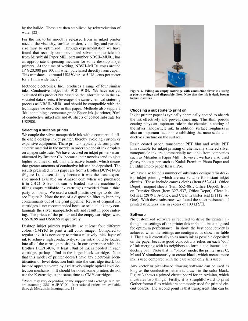
Selecting a suitable printerWe couple the silver nanoparticle ink with a commercial off-the-shelf desktop inkjet printer, thereby avoiding custom orexpensive equipment. These printers typically deform piezo-electric material in the nozzle in order to deposit ink dropletson a paper substrate. We have focused on inkjet printers man-ufactured by Brother Co. because their nozzles tend to ejecthigher volumes of ink than alternative brands, which meansthat greater amounts of conductive ink can be deposited. Theresults presented in this paper are from a Brother DCP–J140w(Figure 1), chosen simply because it was the least expen-sive model available on Amazon.com when we purchasedit in 2012! Silver ink can be loaded into the machine byfilling empty refillable ink cartridges provided from a thirdparty company. We used a small plastic syringe to do this,see Figure 2. Note the use of a disposable filter to keep anycontaminants out of the print pipeline. Reuse of original inkcartridges is not recommended because residual ink may con-taminate the silver nanoparticle ink and result in poor sinter-ing. The prices of the printer and the empty cartridges wereUS$76.99 and US$8.99 respectively.
Desktop inkjet printers typically use at least four differentcolors (CMYK) to print a full color image. Compared toregular ink, it is necessary to print a relatively thick layer ofink to achieve high conductivity, so the ink should be loadedinto all of the cartridge positions. In our experience with theBrother DCPJ140w, at least 10ml of ink is needed in eachcartridge, perhaps 15ml in the larger black cartridge. Notethat this model of printer doesn’t have any electronic iden-tification or level detection built into the cartridge itself, butinstead appears to employ a relatively simple optical level de-tection mechanism. It should be noted some printers do notuse the K cartridge at the same time as CMY cartridges.2Prices may vary depending on the supplier and exchange rate, weare assuming US$1 = JP U100. International orders are availablethrough Mitsubishi Imaging, Inc. [1].
Figure 2. Filling an empty cartridge with conductive silver ink usinga plastic syringe and disposable filter. Note that the ink is dark brownbefore it sinters.
Choosing a substrate to print onInkjet printer paper is typically chemically coated to absorbthe ink effectively and prevent smearing. This thin, porouscoating plays an important role in the chemical sintering ofthe silver nanoparticle ink. In addition, surface roughness isalso an important factor in establishing the nano-scale con-ductive structure on the surface.
Resin coated paper, transparent PET film and white PETfilm suitable for inkjet printing of chemically sintered silvernanoparticle ink are commercially available from companiessuch as Mitsubishi Paper Mill. However, we have also usedglossy photo paper, such as Kodak Premium Photo Paper andFujifilm Photo paper Kassai Pro.
We have also found a number of substrates designed for desk-top inkjet printing which are not suitable for instant inkjetcircuits. These include canvas cloths (Item 652–041, OfficeDepot), magnet sheets (Item 652–061, Office Depot), Iron-on Transfer Sheet (Item 327–537, Office Depot), Clear la-bel seal (28791, A-One), and Clear Transfer seal (51112, A-One). With these substrates we found the sheet resistance ofprinted structures was in excess of 100 kΩ/.
SoftwareNo customized software is required to drive the printer al-though the settings of the printer driver should be configuredfor optimum performance. In short, the best conductivity isachieved when the settings are configured as shown in Table1. The aim is essentially to as much ink as possible depositedon the paper because good conductivity relies on each ‘dot’of ink merging with its neighbors to form a continuous con-ducting path. Note that in “photo” mode, the printer uses C,M and Y simultaneously to create black, which means moreink is used compared with the case when only K is used.
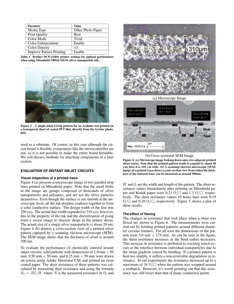
Any vector or pixel-based drawing software can be used aslong as the conductive pattern is drawn in the color black.Figure 3 shows a printed circuit board for an Arduino, whichillustrates two things: Firstly, it is straightforward to printGerber format files which are commonly used for printed cir-cuit boards. The second point is that transparent film can be
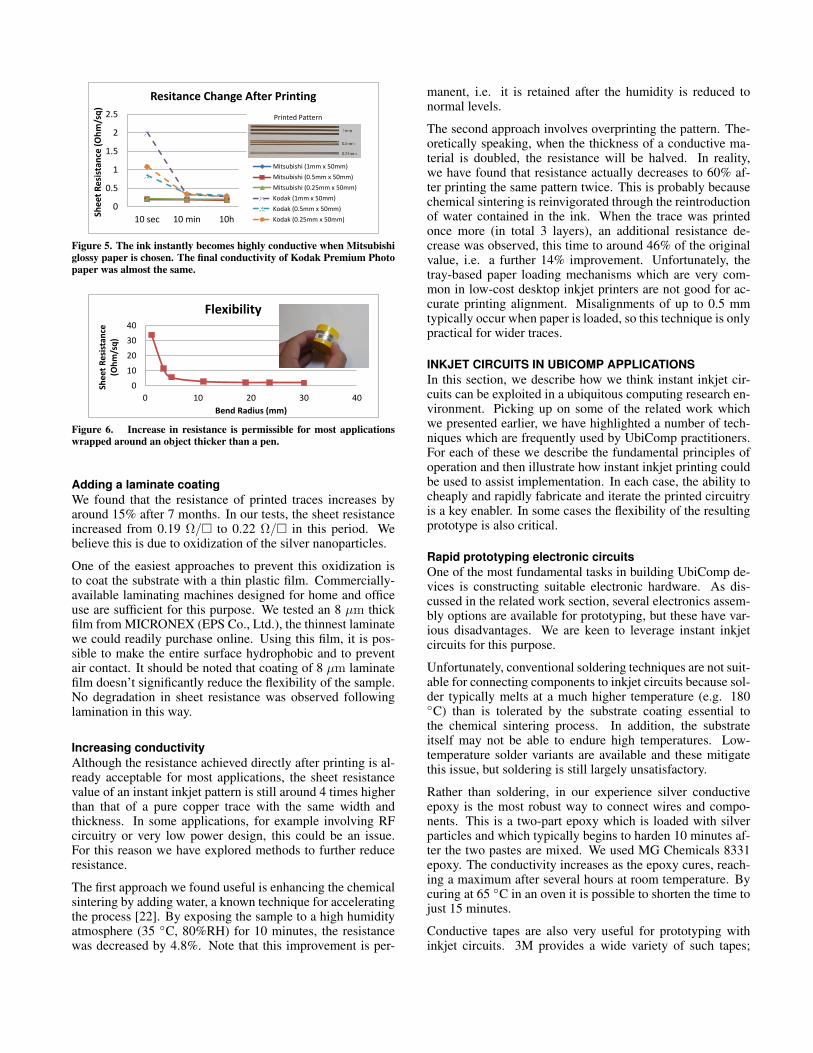
Paramter ValueMedia Type Other Photo PaperPrint Quality BestColor Mode VividColor Enhancement EnableColor Density +2Improve Pattern Printing Enable
Table 1. Brother DCP-J140w printer settings for optimal performancewhen using Mitsubishi NBSIJ-MU01 silver nanoparticle ink.
Figure 3. A single-sided wiring pattern for an Arduino was printed ona transparent sheet of coated PET film, directly from the Gerber photo-plot.
used as a substrate. Of course, in this case although the cir-cuit board is flexible, components like the microcontroller arenot, so it is not possible to make the entire board bendable.We will discuss methods for attaching components in a latersection.
EVALUATION OF INSTANT INKJET CIRCUITS
Visual inspection of a printed traceFigure 4 (a) presents a microscope image of two parallel striplines printed on Mitsubishi paper. Note that the small blobsin the image are groups composed of thousands of silvernanoparticles and polymers, and are not the silver particlesthemselves. Even though the surface is not smooth at the mi-croscopic level, all the ink droplets coalesce together to forma solid conductive surface. The design width of the line was250 µm. The actual line width expanded to 310 µm, however,due to the property of the ink and the discretization of goingfrom a vector image to discrete drops in the printer driver.The actual size of a single silver nanoparticle is about 20 nm.Figure 4 (b) depicts a cross-section view of a printed silverpattern captured by a scanning electron microscope (SEM).The SEM image shows that the thickness of silver is around300 nm.
To evaluate the performance of chemically sintered instantinkjet circuits, solid patterns with dimensions of 1.0 mm × 50mm, 0.50 mm × 50 mm, and 0.25 mm × 50 mm were drawnon-screen using Adobe Illustrator CS6 and printed on resincoated paper. The sheet resistance of these patterns was cal-culated by measuring their resistance and using the formulaRs = RL/W where R is the measured resistance in Ω, and
(a) Microscope Image
Paper
Silver
(b) Cross-sectional SEM ImageFigure 4. (a) Microscope image looking down onto two adjacent printedsilver traces. Note that the printed pattern tends to expand by about 60µm, here it is 310 µm wide. (b) A scanning electron microscope (SEM)image of a printed trace shows a cross-section view from which the thick-ness of the sintered trace can be measured at around 300nm.
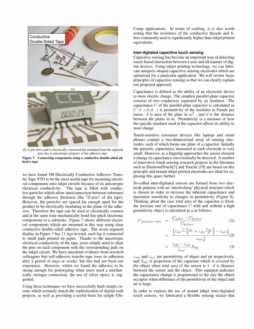
W andL are the width and length of the pattern. The sheet re-sistance values immediately after printing on Mitsubishi pa-per and Kodak paper were 0.21 Ω/ and 1.3 Ω/, respec-tively. The sheet resistance values 10 hours later were 0.19Ω/ and 0.28 Ω/, respectively. Figure 5 shows a plot ofthese results.
The effect of flexingThe changes in resistance that took place when a sheet wasflexed are shown in Figure 6. The measurements were car-ried out by bending printed patterns around different diame-ter circular formers. For all tests the dimensions of the pat-tern were 5.0 mm × 174 mm. As can be seen in the figure,the sheet resistance increases as the bend radius decreases.This increase in resistance is attributed to cracking which oc-curs at the interface between individual nanoparticles due tothe strain gradient caused by bending. If a printed pattern isbent too sharply, it suffers a non-reversible degradation in re-sistance. In our experiments the resistance increased up to amaximum of 34 Ω/ when the pattern was wrapped arounda toothpick. However, it’s worth pointing out that this resis-tance was still lower than that of many conductive paints.
0
0.5
1
1.5
2
2.5
10 sec 10 min 10hSheet R
esistance (Ohm
/sq)
Resitance Change After Printing
Mitsubishi (1mm x 50mm)Mitsubishi (0.5mm x 50mm)Mitsubishi (0.25mm x 50mm)Kodak (1mm x 50mm)Kodak (0.5mm x 50mm)Kodak (0.25mm x 50mm)
Printed Pattern
Figure 5. The ink instantly becomes highly conductive when Mitsubishiglossy paper is chosen. The final conductivity of Kodak Premium Photopaper was almost the same.
0
10
20
30
40
0 10 20 30 40
Sheet R
esistance
(Ohm
/sq)
Bend Radius (mm)
Flexibility
Figure 6. Increase in resistance is permissible for most applicationswrapped around an object thicker than a pen.
Adding a laminate coatingWe found that the resistance of printed traces increases byaround 15% after 7 months. In our tests, the sheet resistanceincreased from 0.19 Ω/ to 0.22 Ω/ in this period. Webelieve this is due to oxidization of the silver nanoparticles.
One of the easiest approaches to prevent this oxidization isto coat the substrate with a thin plastic film. Commercially-available laminating machines designed for home and officeuse are sufficient for this purpose. We tested an 8 µm thickfilm from MICRONEX (EPS Co., Ltd.), the thinnest laminatewe could readily purchase online. Using this film, it is pos-sible to make the entire surface hydrophobic and to preventair contact. It should be noted that coating of 8 µm laminatefilm doesn’t significantly reduce the flexibility of the sample.No degradation in sheet resistance was observed followinglamination in this way.
Increasing conductivityAlthough the resistance achieved directly after printing is al-ready acceptable for most applications, the sheet resistancevalue of an instant inkjet pattern is still around 4 times higherthan that of a pure copper trace with the same width andthickness. In some applications, for example involving RFcircuitry or very low power design, this could be an issue.For this reason we have explored methods to further reduceresistance.
The first approach we found useful is enhancing the chemicalsintering by adding water, a known technique for acceleratingthe process [22]. By exposing the sample to a high humidityatmosphere (35 C, 80%RH) for 10 minutes, the resistancewas decreased by 4.8%. Note that this improvement is per-
manent, i.e. it is retained after the humidity is reduced tonormal levels.
The second approach involves overprinting the pattern. The-oretically speaking, when the thickness of a conductive ma-terial is doubled, the resistance will be halved. In reality,we have found that resistance actually decreases to 60% af-ter printing the same pattern twice. This is probably becausechemical sintering is reinvigorated through the reintroductionof water contained in the ink. When the trace was printedonce more (in total 3 layers), an additional resistance de-crease was observed, this time to around 46% of the originalvalue, i.e. a further 14% improvement. Unfortunately, thetray-based paper loading mechanisms which are very com-mon in low-cost desktop inkjet printers are not good for ac-curate printing alignment. Misalignments of up to 0.5 mmtypically occur when paper is loaded, so this technique is onlypractical for wider traces.
INKJET CIRCUITS IN UBICOMP APPLICATIONSIn this section, we describe how we think instant inkjet cir-cuits can be exploited in a ubiquitous computing research en-vironment. Picking up on some of the related work whichwe presented earlier, we have highlighted a number of tech-niques which are frequently used by UbiComp practitioners.For each of these we describe the fundamental principles ofoperation and then illustrate how instant inkjet printing couldbe used to assist implementation. In each case, the ability tocheaply and rapidly fabricate and iterate the printed circuitryis a key enabler. In some cases the flexibility of the resultingprototype is also critical.
Rapid prototyping electronic circuitsOne of the most fundamental tasks in building UbiComp de-vices is constructing suitable electronic hardware. As dis-cussed in the related work section, several electronics assem-bly options are available for prototyping, but these have var-ious disadvantages. We are keen to leverage instant inkjetcircuits for this purpose.
Unfortunately, conventional soldering techniques are not suit-able for connecting components to inkjet circuits because sol-der typically melts at a much higher temperature (e.g. 180C) than is tolerated by the substrate coating essential tothe chemical sintering process. In addition, the substrateitself may not be able to endure high temperatures. Low-temperature solder variants are available and these mitigatethis issue, but soldering is still largely unsatisfactory.
Rather than soldering, in our experience silver conductiveepoxy is the most robust way to connect wires and compo-nents. This is a two-part epoxy which is loaded with silverparticles and which typically begins to harden 10 minutes af-ter the two pastes are mixed. We used MG Chemicals 8331epoxy. The conductivity increases as the epoxy cures, reach-ing a maximum after several hours at room temperature. Bycuring at 65 C in an oven it is possible to shorten the time tojust 15 minutes.
Conductive tapes are also very useful for prototyping withinkjet circuits. 3M provides a wide variety of such tapes;
(a)
(b) A pin and a pad is electrically connected but insulated from the adjacentpins due to anisotropic property of the adhesive tape.
Figure 7. Connecting components using a conductive double-sided ad-hesive tape.
we have found 3M Electrically Conductive Adhesive Trans-fer Tape 9703 to be the most useful tape for mounting electri-cal components onto inkjet circuits because of its anisotropicelectrical conductivity. The tape is filled with conduc-tive particles which allow interconnection between substratesthrough the adhesive thickness (the “Z-axis” of the tape).However, the particles are spaced far enough apart for theproduct to be electrically insulating in the plane of the adhe-sive. Therefore the tape can be used to electrically connectand at the same time mechanically bond fine-pitch electroniccomponents to a substrate. Figure 7 shows different electri-cal components which are mounted in this way using clearconductive double-sided adhesive tape. The seven segmentdisplay in Figure 7 has 11 legs in total; each leg is connectedto small pads printed on paper. Thanks to the anisotropicelectrical conductivity of the tape, users simply need to alignthe pins on each component with the corresponding pads onthe inkjet circuit. We have anecdotal evidence from researchcolleagues that self-adhesive transfer tape loses its adhesionafter a period of days or weeks, but this had not been ourexperience. However, whilst we found the adhesive to bestrong enough for prototyping when users need a mechan-ically stronger connection, the use of silver epoxy is sug-gested.
Using these techniques we have successfully built simple cir-cuits which certainly match the sophistication of digital craftprojects, as well as providing a useful basis for simple Ubi-
Comp applications. In terms of crafting, it is also worthnoting that the resistance of the conductive threads and fi-bres commonly used is significantly higher than inkjet printedequivalents.
Inter-digitated capacitive touch sensingCapacitive sensing has become an important way of detectingtouch-based interaction between a user and all manner of dig-ital devices. Using inkjet printing technology, we can fabri-cate uniquely-shaped capacitive sensing electrodes which areoptimized for a particular application. We will review basicprinciples of capacitive sensing so that we can clearly explainour proposed approach.
Capacitance is defined as the ability of an electronic deviceto store electric charge. The simplest parallel-plate capacitorconsists of two conductors separated by an insulator. Thecapacitance C of the parallel-plate capacitor is calculated asC ≈ εA/d. ε is permittivity of the insulator in Farads permeter, A is area of the plate in m2 , and d is the distancebetween the plates in m. Permittivity is a measure of howthe specific insulator used in the capacitor affects its ability tostore charge.
Touch-sensitive consumer devices like laptops and smartphones contain a two-dimensional array of sensing elec-trodes, each of which forms one plate of a capacitor. Initiallythe parasitic capacitance measured at each electrode is verysmall. However, as a fingertip approaches the sensor elementa change in capacitance can eventually be detected. A numberof innovative touch sensing research projects in the literaturesuch as DiamondTouch[7] and Touche [19] are based on thisprinciple and instant inkjet printed electrodes are ideal for ex-ploring this space further.
So-called inter-digitated sensors are formed from two elec-trode patterns with an ‘interlocking’ physical structure whichis chosen in order to increase the inherent capacitance andmaximize sensitivity to changes in permittivity (Figure 8).Thinking about the case total area of the capacitor is fixed,the increase rate of capacitance C with and without a highpermittivity object is calculated as a as follows:
Cincrease rate =Cafter − Cbefore
Cbefore(1)
=
(εair
1−Sobj
d + εobjSobj
d
)− εair
1d
εair1d
(2)
=εobj − εair
εairSobj (3)
εobj and εair are permittivity of object and air respectively,and Sobj is proportion of the capacitor which is covered bythe object when total area of the sensor is 1. d is distancebetween the sensor and the object. This equation indicatesthe capacitance change is proportional to the size the objectoccupies when difference of the permittivity of the object andair is large.
In order to explore the use of instant inkjet inter-digitatedtouch sensors, we fabricated a flexible sensing sticker that
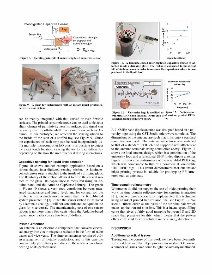
Figure 8. Operating principle of an inter-digitated capacitive sensor.
Figure 9. A plush toy instrumented with an instant inkjet printed ca-pacitive sensor ribbon.
can be readily integrated with flat, curved or even flexiblesurfaces. The printed sensor electrode can be used to detect aslight change of permittivity near its surface; this signal canbe easily read by off-the-shelf microcontrollers such as Ar-duino. In our prototype, we attached the sensing ribbon tothe inside of the skin of a stuffed toy, see Figure 9. Sincethe capacitance of each strip can be read independently us-ing multiple microcontroller I/O pins, it is possible to detectthe exact touch location, causing the toy to react differentlydepending on the how the user touches it during interactions.
Capacitive sensing for liquid level detectionFigure 10 shows another example application based on aribbon-shaped inter-digitated sensing sticker. A laminate-coated sensor strip is attached to the inside of a drinking glass.The flexibility of the ribbon allows it to fit to the curved sur-face of the glass. Its capacitance is measured using an Ar-duino nano and the Arudino CapSense Library. The graphin Figure 10 shows a very good correlation between mea-sured capacitance and liquid level, and for comparison theprinted sensor is much more accurate than the RFID-basedsystem presented in [3]. Since the sensor ribbon is insulatedby a laminate coating, it will not contaminate the liquid in theglass (or vice-versa). The manufacturing cost of one sensorribbon is no more than a few cents while the Arduino-basedcapacitance reader costs a few tens of dollars.
Printed AntennasAn antenna is an electronic component that converts electri-cal energy into electromagnetic radiation in the form of radiowaves and vice-versa. The simplest antennas consist of onlyan arrangement of metallic conductors, and in this case theconductivity, permittivity and shape of the antenna has a hugebearing on its performance.
0
0.5
1
1.5
2
0 50 100
Capa
citance (nF)
Liquid Level (mm)
Figure 10. A laminate-coated inter-digitated capacitive ribbon is at-tached inside a drinking glass. The ribbon is connected to the digitalI/O of Arduino nano in order to measure the capacitance which is pro-portional to the liquid level
Figure 11. University logo is modified as915MHz UHF band antenna. RFID chip isattached using conductive epoxy.
15 20 25 30 35
50 75 100 125
Power (d
Bm)
Range (cm)
Minimum Power Level to Read Tag
Figure 12. Performanceof custom printed RFIDtag.
A 915MHz band dipole antenna was designed based on a uni-versity logo using the CST Studio microwave simulator. Thedimensions of the antenna are such that it fits onto a standardsized business card. The antenna impedance was matchedto that of a standard RFID chip to support direct attachmentto the antenna terminals using conductive epoxy. Figure 11shows the final antenna design, which is a combination of theuniversity logo and a functional UHF folded dipole antenna.Figure 12 shows the performance of the assembled RFID tag,which was comparable to that of a commercial low-profileUHF RFID tags. This result demonstrates that our instantinkjet printing process is suitable for prototyping RF struc-tures such as antennas.
Time domain reflectometryWimmer et al. did not suggest the use of inkjet printing theirwork on time domain reflectrometry for sensing interaction[21], but we have successfully implemented this techniqueusing an inkjet printed transmission line, see Figure 13. Weused a Hilbert curve as the basis of the stripline pair whichmakes up the transmission line. This is a fractal space-fillingcurve that gives a fairly good mapping between 1D and 2Dspace that preserves locality, which means that the patternoffers consistent touch resolution in the x and y directions.
DISCUSSION
Additional practical issuesThroughout the course of this work we have been pleasantlysurprised how well the inkjet process has worked. Of course,a number of issues have come to light. As already mentioned,
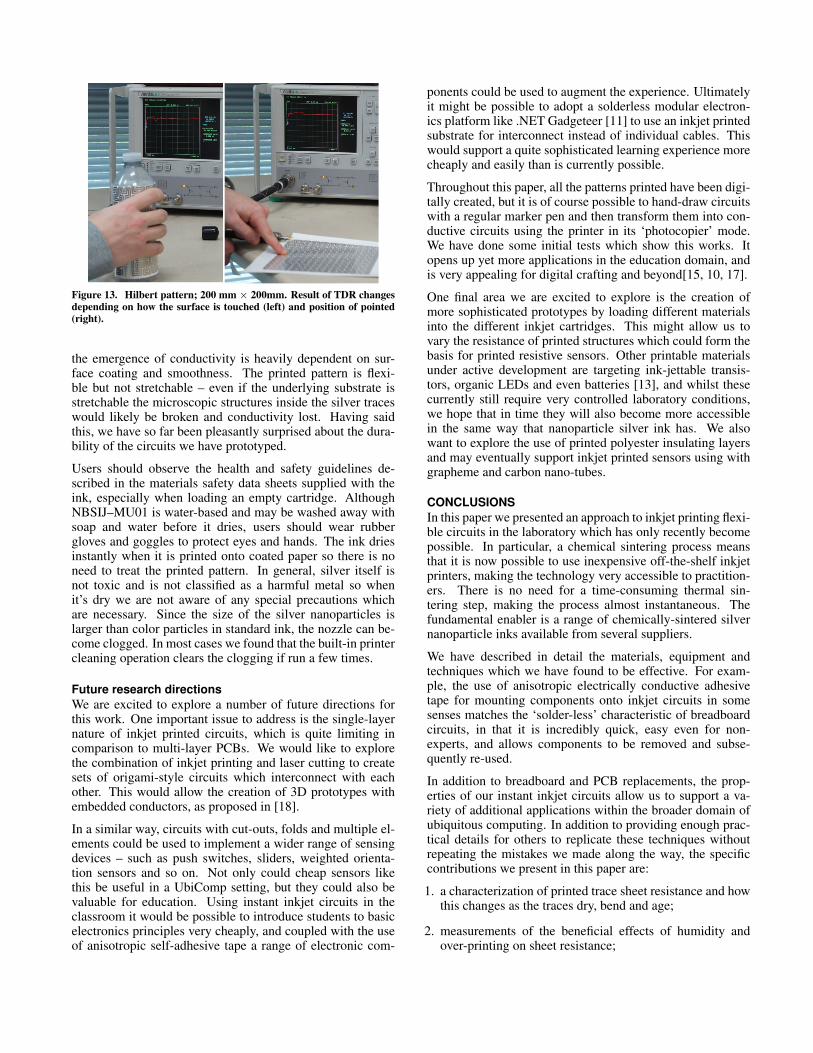
Figure 13. Hilbert pattern; 200 mm × 200mm. Result of TDR changesdepending on how the surface is touched (left) and position of pointed(right).
the emergence of conductivity is heavily dependent on sur-face coating and smoothness. The printed pattern is flexi-ble but not stretchable – even if the underlying substrate isstretchable the microscopic structures inside the silver traceswould likely be broken and conductivity lost. Having saidthis, we have so far been pleasantly surprised about the dura-bility of the circuits we have prototyped.
Users should observe the health and safety guidelines de-scribed in the materials safety data sheets supplied with theink, especially when loading an empty cartridge. AlthoughNBSIJ–MU01 is water-based and may be washed away withsoap and water before it dries, users should wear rubbergloves and goggles to protect eyes and hands. The ink driesinstantly when it is printed onto coated paper so there is noneed to treat the printed pattern. In general, silver itself isnot toxic and is not classified as a harmful metal so whenit’s dry we are not aware of any special precautions whichare necessary. Since the size of the silver nanoparticles islarger than color particles in standard ink, the nozzle can be-come clogged. In most cases we found that the built-in printercleaning operation clears the clogging if run a few times.
Future research directionsWe are excited to explore a number of future directions forthis work. One important issue to address is the single-layernature of inkjet printed circuits, which is quite limiting incomparison to multi-layer PCBs. We would like to explorethe combination of inkjet printing and laser cutting to createsets of origami-style circuits which interconnect with eachother. This would allow the creation of 3D prototypes withembedded conductors, as proposed in [18].
In a similar way, circuits with cut-outs, folds and multiple el-ements could be used to implement a wider range of sensingdevices – such as push switches, sliders, weighted orienta-tion sensors and so on. Not only could cheap sensors likethis be useful in a UbiComp setting, but they could also bevaluable for education. Using instant inkjet circuits in theclassroom it would be possible to introduce students to basicelectronics principles very cheaply, and coupled with the useof anisotropic self-adhesive tape a range of electronic com-
ponents could be used to augment the experience. Ultimatelyit might be possible to adopt a solderless modular electron-ics platform like .NET Gadgeteer [11] to use an inkjet printedsubstrate for interconnect instead of individual cables. Thiswould support a quite sophisticated learning experience morecheaply and easily than is currently possible.
Throughout this paper, all the patterns printed have been digi-tally created, but it is of course possible to hand-draw circuitswith a regular marker pen and then transform them into con-ductive circuits using the printer in its ‘photocopier’ mode.We have done some initial tests which show this works. Itopens up yet more applications in the education domain, andis very appealing for digital crafting and beyond[15, 10, 17].
One final area we are excited to explore is the creation ofmore sophisticated prototypes by loading different materialsinto the different inkjet cartridges. This might allow us tovary the resistance of printed structures which could form thebasis for printed resistive sensors. Other printable materialsunder active development are targeting ink-jettable transis-tors, organic LEDs and even batteries [13], and whilst thesecurrently still require very controlled laboratory conditions,we hope that in time they will also become more accessiblein the same way that nanoparticle silver ink has. We alsowant to explore the use of printed polyester insulating layersand may eventually support inkjet printed sensors using withgrapheme and carbon nano-tubes.
CONCLUSIONSIn this paper we presented an approach to inkjet printing flexi-ble circuits in the laboratory which has only recently becomepossible. In particular, a chemical sintering process meansthat it is now possible to use inexpensive off-the-shelf inkjetprinters, making the technology very accessible to practition-ers. There is no need for a time-consuming thermal sin-tering step, making the process almost instantaneous. Thefundamental enabler is a range of chemically-sintered silvernanoparticle inks available from several suppliers.
We have described in detail the materials, equipment andtechniques which we have found to be effective. For exam-ple, the use of anisotropic electrically conductive adhesivetape for mounting components onto inkjet circuits in somesenses matches the ‘solder-less’ characteristic of breadboardcircuits, in that it is incredibly quick, easy even for non-experts, and allows components to be removed and subse-quently re-used.
In addition to breadboard and PCB replacements, the prop-erties of our instant inkjet circuits allow us to support a va-riety of additional applications within the broader domain ofubiquitous computing. In addition to providing enough prac-tical details for others to replicate these techniques withoutrepeating the mistakes we made along the way, the specificcontributions we present in this paper are:
1. a characterization of printed trace sheet resistance and howthis changes as the traces dry, bend and age;
2. measurements of the beneficial effects of humidity andover-printing on sheet resistance;

3. a discussion of techniques for attaching electronic compo-nents to printed traces;
4. an illustration of capacitive sensing using printed elec-trodes for touch, multi-touch and liquid level detection;
5. a demonstration of using printed UHF structures such asRFID tag antennas and transmission lines; and
6. a number of directions for future work.
We hope that others working in the field of ubiquitous com-puting will be excited to look for opportunities to leverage in-stant inkjet printing for the projects they are working on, andwill be inspired to take the ideas we presented in this paper innew and exciting directions.
ACKNOWLEDGMENTSWe would like to thank those who gave us a lot of useful tech-nical suggestions and comments: Mr. Shigeki Shino, Prof.Tsuyoshi Sekitani, Dr. Kevin Li, Prof. Masahiko Inami, Prof.Joseph Paradiso, and anonymous reviewers.
This research was supported in part by the Industrial Technol-ogy Research Grant Program, 2009, of the New Energy andIndustrial Technology Development Organization (NEDO) ofJapan and JSPS KAKENHI Grant Numbers 25280027.
REFERENCES1. Mitsubishi imaging, inc.
http://www.mitsubishiimaging.com/digital-imaging-diamond-jet-NANOINK.html.
2. Bare paint. http://www.bareconductive.com/.
3. Bhattacharyya, R., Floerkemeier, C., and Sarma, S.RFID tag antenna based sensing: Does your beverageglass need a refill? In Proc. of IEEE RFID 2010, IEEE(Apr. 2010), 126–133.
4. Bhattacharyya, R., Floerkemeier, C., and Sarma, S. Rfidtag antenna based temperature sensing. In Proc. of IEEERFID 2010, IEEE (2010), 8–15.
5. Coelho, M., Hall, L., Berzowska, J., and Maes, P.Pulp-based computing: a framework for buildingcomputers out of paper. In Proc. of CHI EA ’09, ACMPress (Apr. 2009), 3527–3528.
6. Circuitworks conductive pen.http://www.chemtronics.com/products/product.asp?r=1&m=2&id=7.
7. Dietz, P., and Leigh, D. DiamondTouch: A Multi-UserTouch Technology. In Proc. of UIST ’01, ACM Press(Nov. 2001), 219–226.
8. Dimatix Material Printer DMP-2831. http://www.fujifilmusa.com/products/industrial_inkjet_printheads/deposition-products/dmp-2800/.
9. Ford, M. Can the ‘silver bullet’ of printing revolutionizeelectronics? Digital Biz, CNN, December 10th, 2009.,http://www.cnn.com/2009/TECH/12/09/electronics.printer.xerox/.
10. Gong, N.-W., Hodges, S., and Paradiso, J. A. Leveragingconductive inkjet technology to build a scalable andversatile surface for ubiquitous sensing. In Proc. ofUbiComp ’11, ACM Press (Sept. 2011), 45–54.
11. Hodges, S., Scott, J., Sentance, S., Miller, C., Villar, N.,Schwiderski-Grosche, S., Hammil, K., and Johnston, S..net gadgeteer: a new platform for k-12 computerscience education. In SIGCSE (2013), 391–396.
12. Holman, D., and Vertegaal, R. TactileTape: low-costtouch sensing on curved surfaces. In Adjunct Proc. ofUIST ’11, ACM Press (Oct. 2011), 17–18.
13. Jablonski, C. Printable batteries. ZDNet, July 17th,2009., http://www.zdnet.com/blog/emergingtech/printable-batteries/1648.
14. LPKF Promat Series. http://www.lpkf.com/.
15. Olberding, S., Gong, N.-W., Tiab, J., Paradiso, J. A., andSteimle, J. A cuttable multi-touch sensor. In Proc.UIST’2013, ACM Press (Oct. 2013).
16. Perner-Wilson, H., Buechley, L., and Satomi, M.Handcrafting textile interfaces from a kit-of-no-parts. InProc. of TEI ’11, ACM Press (Jan. 2011), 61–68.
17. Qi, J., and Buechley, L. Electronic popables: exploringpaper-based computing through an interactive pop-upbook. In Proc. of TEI ’10, ACM Press (Jan. 2010),121–128.
18. Sarik, J., Butler, A., Villar, N., Scott, J., and Hodges, S.Combining 3D printing and printable electronics. InProc. of TEI ’12 Works in Progress, ACM Press (Feb.2012), 1–5.
19. Sato, M., Poupyrev, I., and Harrison, C. Touche:enhancing touch interaction on humans, screens, liquids,and everyday objects. In Proc. of CHI ’12, ACM Press(May 2012), 483–492.
20. Savage, V., Zhang, X., and Hartmann, B. Midas:fabricating custom capacitive touch sensors to prototypeinteractive objects. Proc. of UIST ’12 (2012), 579–588.
21. Wimmer, R., and Baudisch, P. Modular and deformabletouch-sensitive surfaces based on time domainreflectometry. In Proc. of UIST ’11, ACM Press (Oct.2011), 517–526.
22. Yoshiki, T., Shino, S., and Kobayashi, K. Process forpreparing conductive material, United States Patent, US8012676 B2, 2011.