Embed Size (px)
Citation preview
Integrating Condensed Matter Physics into a Liberal Arts
Physics Curriculum
Jeffrey CollettLawrence University
Appleton, WI
March Meeting of the American Physical Society
March 11, 2008
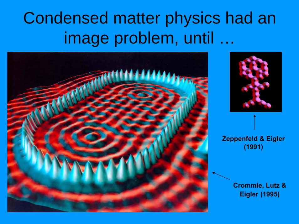
Condensed matter physics had an image problem, until …
Zeppenfeld & Eigler(1991)
Crommie, Lutz & Eigler (1995)
Challenges for Educators• Attract more students to STEM disciplines • Communicate the increasingly
interdisciplinary nature of scientific research
Nanoscience and nanotechnology have opened a new window into
public consciousness.
Special Challenges in Liberal Arts Colleges
• BA physics majors typically take no more than 10-14 physics courses.
• Specialization into subfields is not built into the curriculum, but instead comes with collaborative work with a faculty member.
• Limited potential to introduce new, specialized courses.
• New approaches need to be integrated into existing curricular structure.
Nanoscience in the Physics Curriculum
• Provides a means to reach out to prospective science students.
• Provides examples of contemporary research problems that can be integrated into standard courses.
• Provides an interdisciplinary flavor.
Signature Programs at Lawrence
• Educational programs that grow from a faculty member’s research expertise
• Use special facilities to connect a broad spectrum of students to an important area of physics. – Recruit prospective students by exposing them to a
contemporary field– Provide experience to all physics majors, not just
those involved in collaborative research.– Provide a distinctive teaching perspective.
Present Programs
• Laser Spectroscopy (John Brandenberger)• Computational Physics (David Cook)
– Began with chaos simulations but is moving to astrophysical modeling.
• Nanoscale Imaging and Structure (Jeff Collett)– Structural measurements with scanning probe
microscopy & X-ray scattering are used to understand condensed matter.
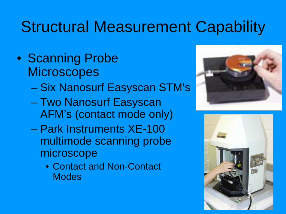
Structural Measurement Capability
• Scanning Probe Microscopes – Six Nanosurf Easyscan STM’s– Two Nanosurf Easyscan
AFM’s (contact mode only)– Park Instruments XE-100
multimode scanning probe microscope
• Contact and Non-Contact Modes
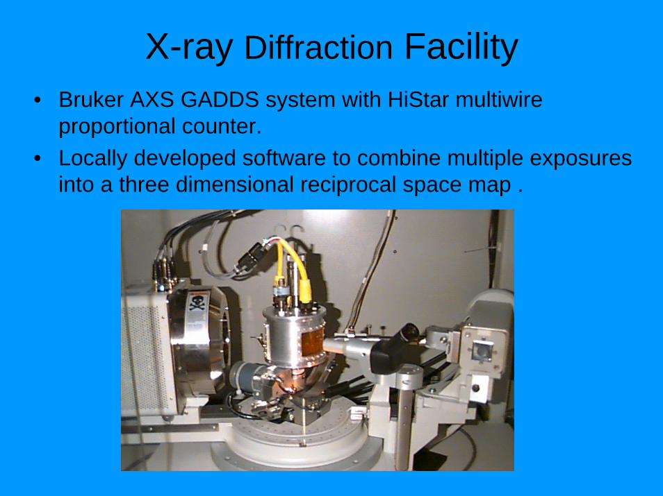
X-ray Diffraction Facility• Bruker AXS GADDS system with HiStar multiwire
proportional counter.• Locally developed software to combine multiple exposures
into a three dimensional reciprocal space map .
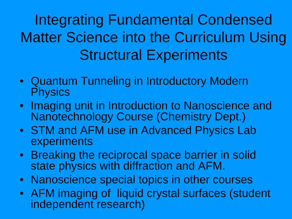
Integrating Fundamental Condensed Matter Science into the Curriculum Using
Structural Experiments
• Quantum Tunneling in Introductory Modern Physics
• Imaging unit in Introduction to Nanoscience and Nanotechnology Course (Chemistry Dept.)
• STM and AFM use in Advanced Physics Lab experiments
• Breaking the reciprocal space barrier in solid state physics with diffraction and AFM.
• Nanoscience special topics in other courses• AFM imaging of liquid crystal surfaces (student
independent research)
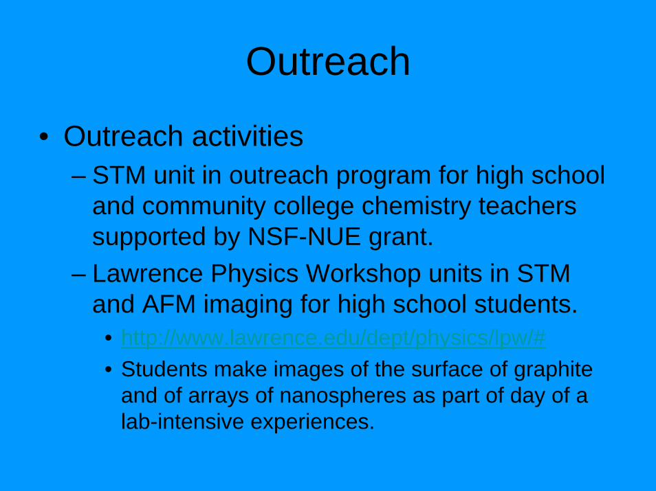
Outreach
• Outreach activities– STM unit in outreach program for high school
and community college chemistry teachers supported by NSF-NUE grant.
– Lawrence Physics Workshop units in STM and AFM imaging for high school students.
• http://www.lawrence.edu/dept/physics/lpw/#• Students make images of the surface of graphite
and of arrays of nanospheres as part of day of a lab-intensive experiences.
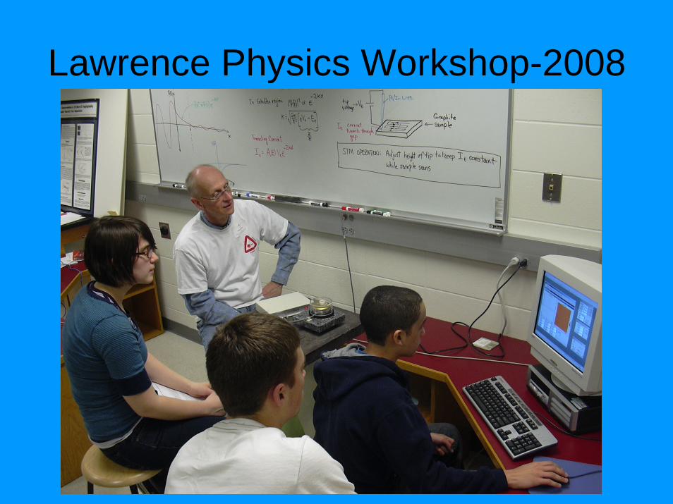
Lawrence Physics Workshop-2008
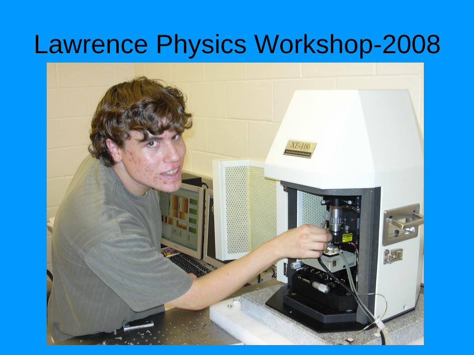
Lawrence Physics Workshop-2008
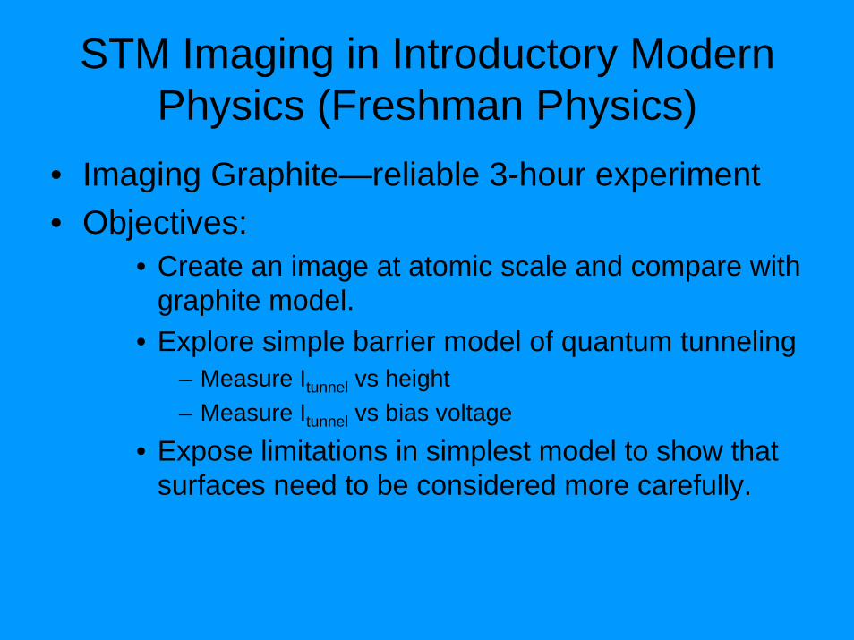
STM Imaging in Introductory Modern Physics (Freshman Physics)
• Imaging Graphite—reliable 3-hour experiment• Objectives:
• Create an image at atomic scale and compare with graphite model.
• Explore simple barrier model of quantum tunneling– Measure Itunnel vs height– Measure Itunnel vs bias voltage
• Expose limitations in simplest model to show that surfaces need to be considered more carefully.
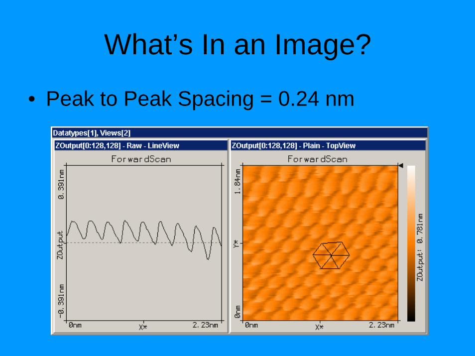
What’s In an Image?
• Peak to Peak Spacing = 0.24 nm
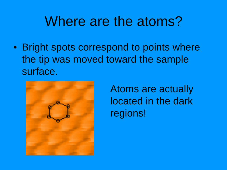
Where are the atoms?
• Bright spots correspond to points where the tip was moved toward the sample surface.
Atoms are actually located in the dark regions!
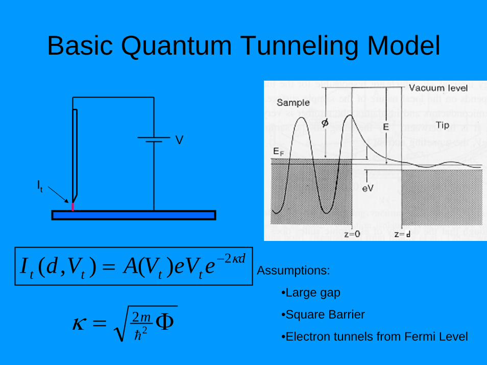
Basic Quantum Tunneling Model
V
It
dtttt eeVVAVdI κ2)(),( −= Assumptions:
•Large gap
•Square Barrier
•Electron tunnels from Fermi LevelΦ= 2
2h
mκ
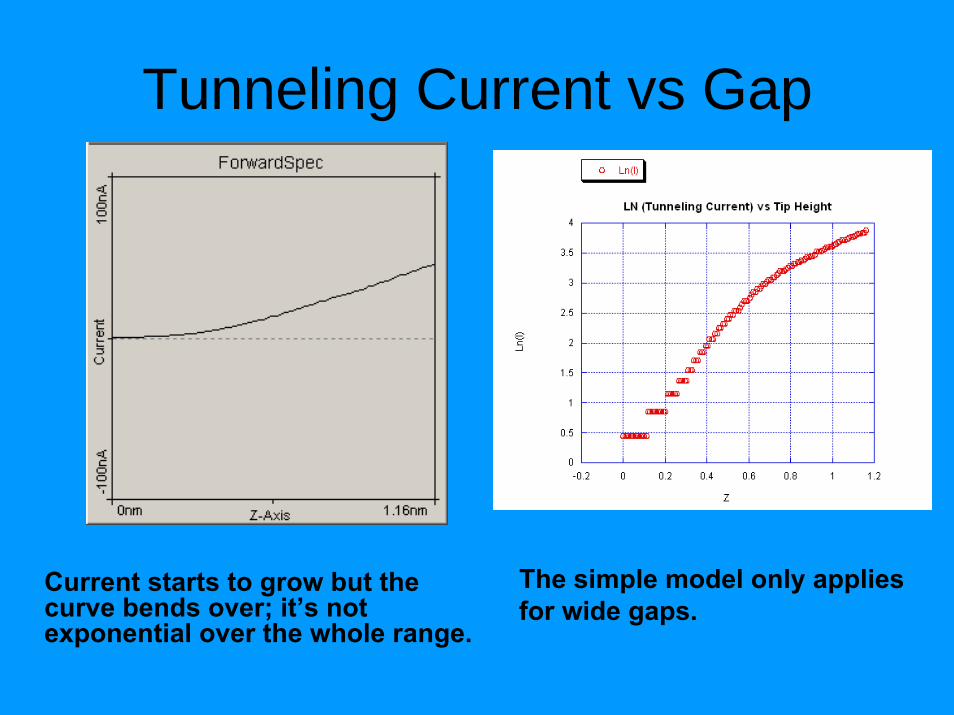
Tunneling Current vs Gap
Current starts to grow but the curve bends over; it’s not exponential over the whole range.
The simple model only applies for wide gaps.
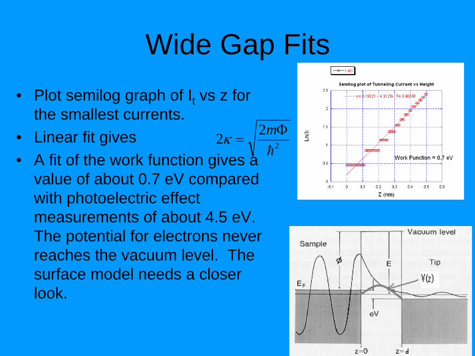
Wide Gap Fits• Plot semilog graph of It vs z for
the smallest currents.• Linear fit gives• A fit of the work function gives a
value of about 0.7 eV compared with photoelectric effect measurements of about 4.5 eV. The potential for electrons never reaches the vacuum level. The surface model needs a closer look.
222h
Φ=
mκ
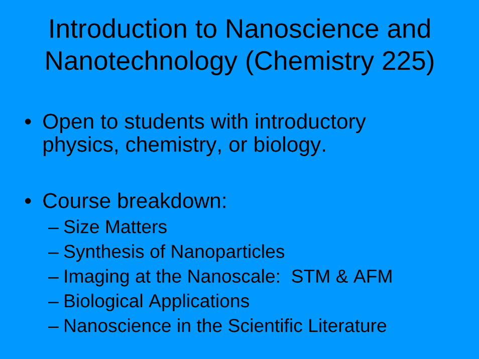
Introduction to Nanoscience and Nanotechnology (Chemistry 225)
• Open to students with introductory physics, chemistry, or biology.
• Course breakdown:– Size Matters– Synthesis of Nanoparticles– Imaging at the Nanoscale: STM & AFM– Biological Applications– Nanoscience in the Scientific Literature
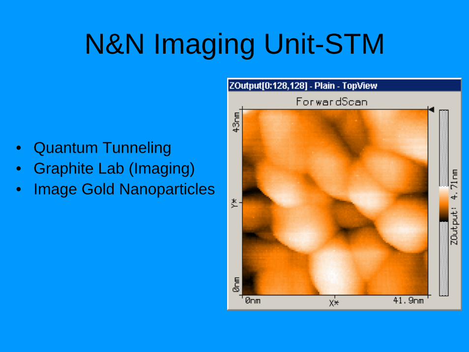
N&N Imaging Unit-STM
• Quantum Tunneling• Graphite Lab (Imaging)• Image Gold Nanoparticles
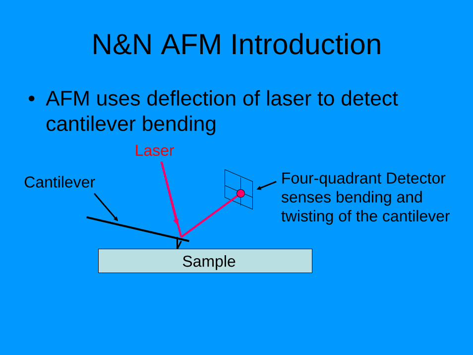
N&N AFM Introduction
• AFM uses deflection of laser to detect cantilever bending
Four-quadrant Detector senses bending and twisting of the cantilever
Sample
Cantilever
Laser
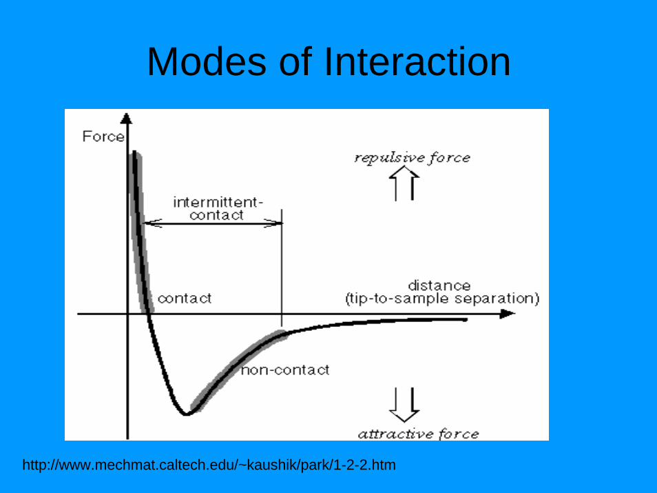
Modes of Interaction
http://www.mechmat.caltech.edu/~kaushik/park/1-2-2.htm
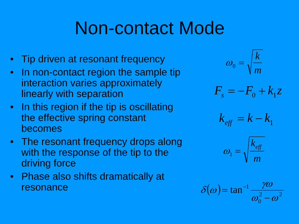
Non-contact Mode• Tip driven at resonant frequency • In non-contact region the sample tip
interaction varies approximately linearly with separation
• In this region if the tip is oscillating the effective spring constant becomes
• The resonant frequency drops along with the response of the tip to the driving force
• Phase also shifts dramatically at resonance
mk
=0ω
zkFFs 10 +−=
1kkkeff −=
mkeff=1ω
( ) 220
1tanωω
γωωδ−
= −
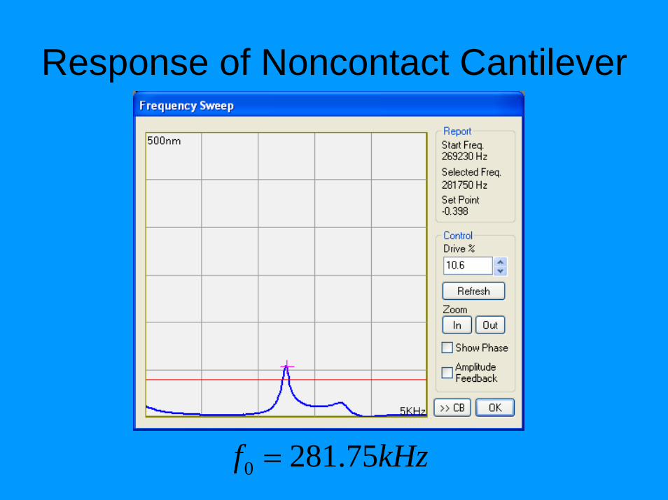
Response of Noncontact Cantilever
kHzf 75.2810 =
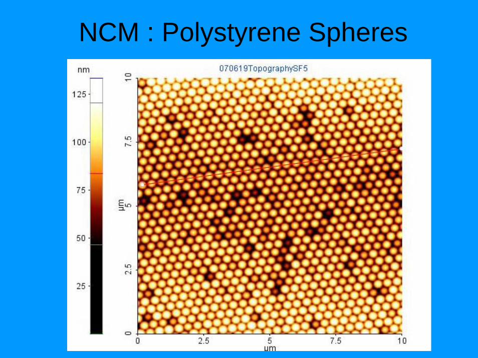
NCM : Polystyrene Spheres
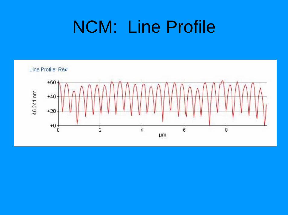
NCM: Line Profile
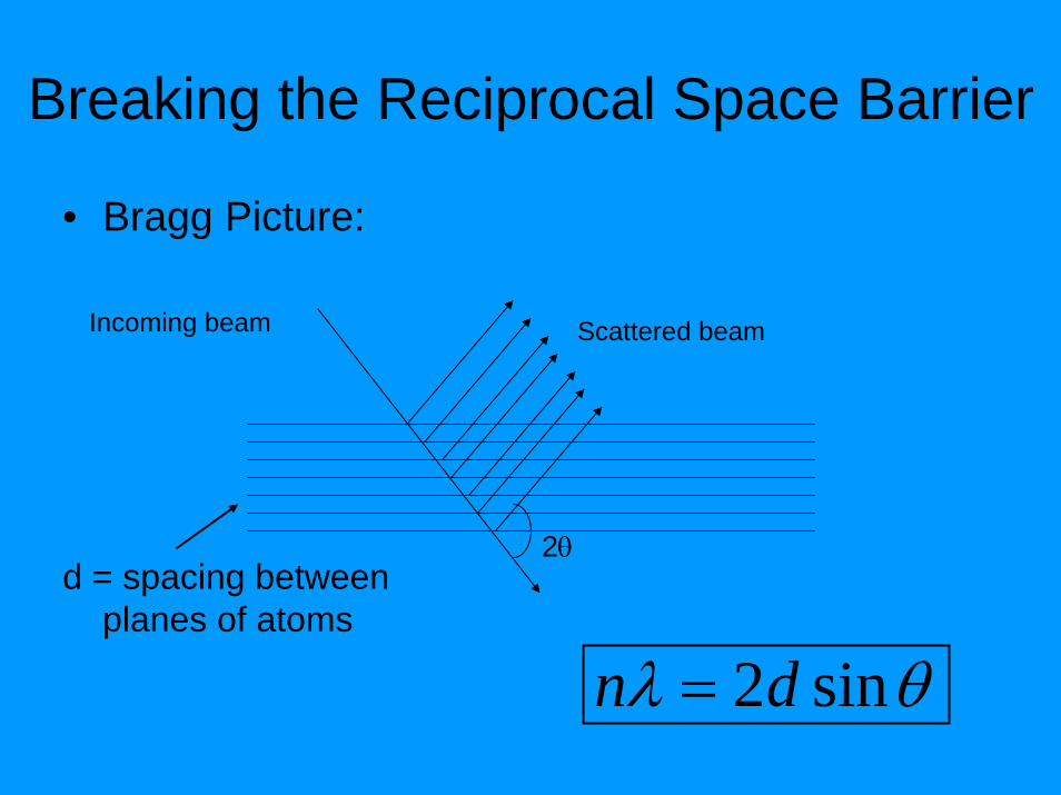
Breaking the Reciprocal Space Barrier
• Bragg Picture:
d = spacing between planes of atoms
θλ sin2dn =
2θ
Incoming beam Scattered beam
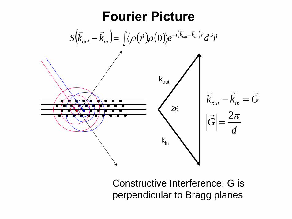
Fourier Picture
dG
Gkk inout
π2=
=−r
rrr
Constructive Interference: G is perpendicular to Bragg planes
kin
kout
2θ
( ) ( ) ( ) ( ) rderkkS rkkiinout
inoutrrrr rrr
30 ⋅−−∫=− ρρ
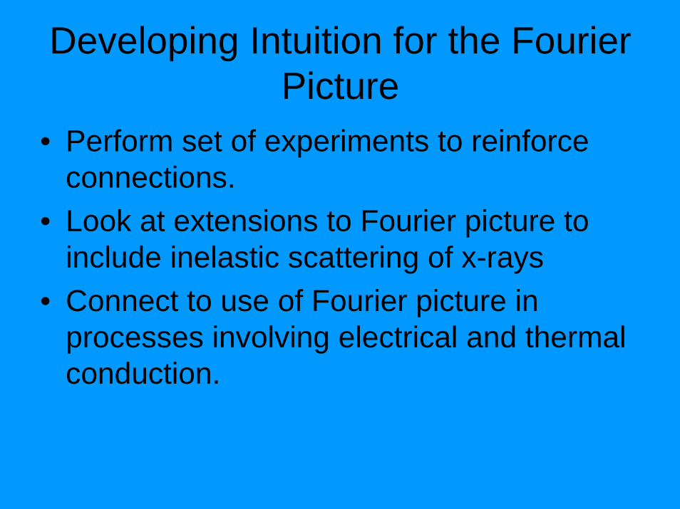
Developing Intuition for the Fourier Picture
• Perform set of experiments to reinforce connections.
• Look at extensions to Fourier picture to include inelastic scattering of x-rays
• Connect to use of Fourier picture in processes involving electrical and thermal conduction.
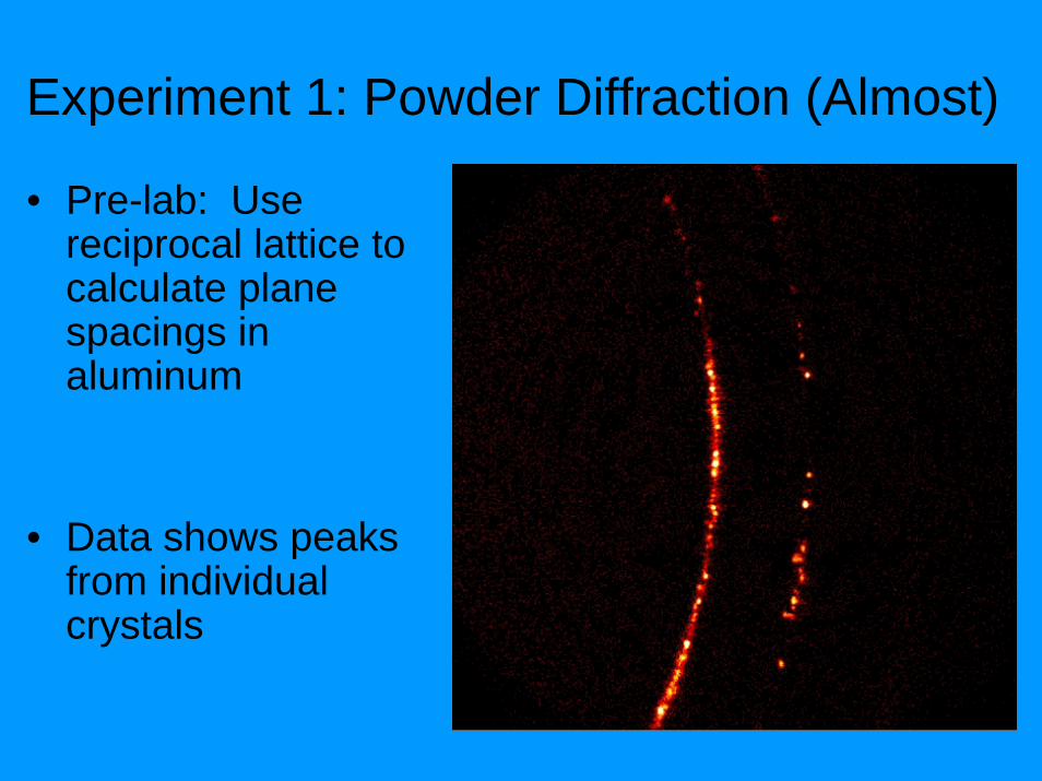
Experiment 1: Powder Diffraction (Almost)
• Pre-lab: Use reciprocal lattice to calculate plane spacings in aluminum
• Data shows peaks from individual crystals
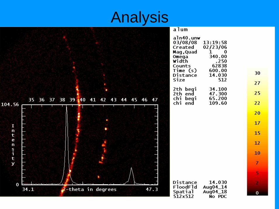
Analysis
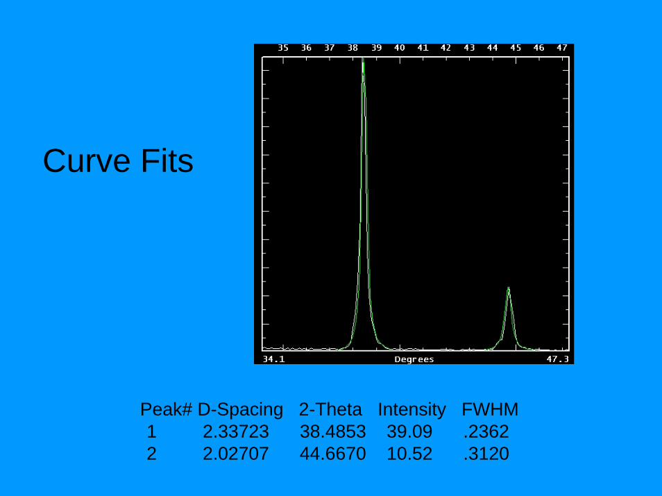
Curve Fits
Peak# D-Spacing 2-Theta Intensity FWHM 1 2.33723 38.4853 39.09 .2362 2 2.02707 44.6670 10.52 .3120
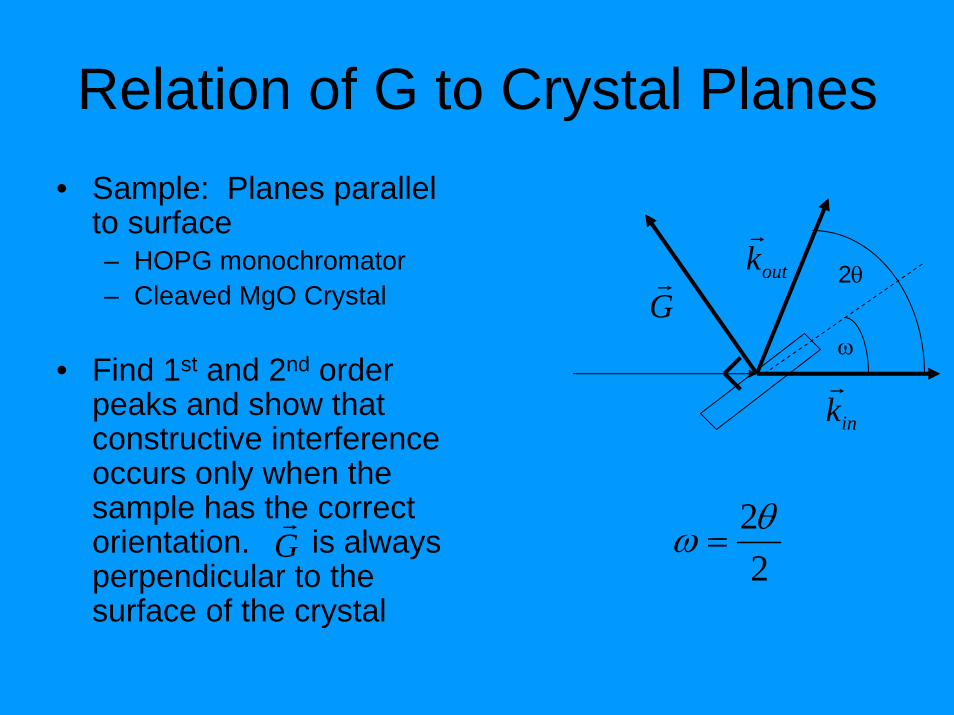
Relation of G to Crystal Planes • Sample: Planes parallel
to surface– HOPG monochromator– Cleaved MgO Crystal
• Find 1st and 2nd order peaks and show that constructive interference occurs only when the sample has the correct orientation. is always perpendicular to the surface of the crystal
22θω =
ω
2θGr outk
r
inkr
Gr
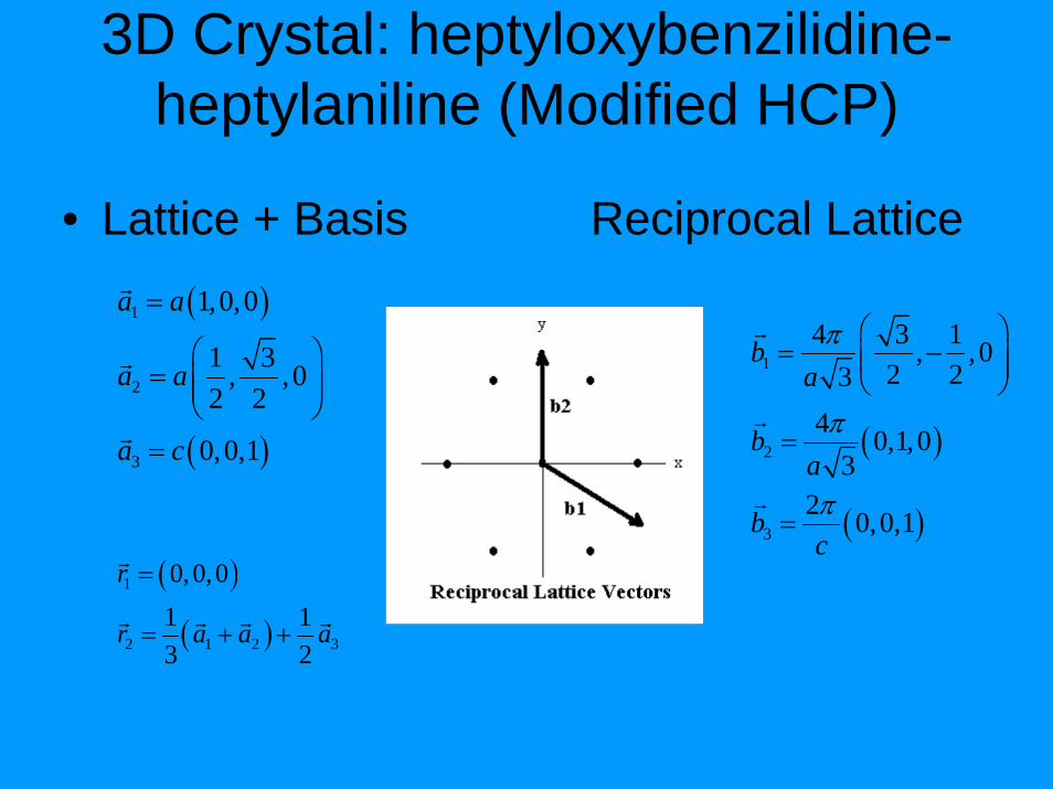
3D Crystal: heptyloxybenzilidine-heptylaniline (Modified HCP)
• Lattice + Basis Reciprocal Lattice
( )
( )
1
2
3
1,0,0
1 3, ,02 2
0,0,1
a a
a a
a c
=
⎛ ⎞= ⎜ ⎟⎜ ⎟
⎝ ⎠=
r
r
r
( )
( )
1
2 1 2 3
0,0,01 13 2
r
r a a a
=
= + +
r
r r r r
( )
( )
1
2
3
4 3 1, ,02 23
4 0,1,03
2 0,0,1
ba
ba
bc
π
π
π
⎛ ⎞= −⎜ ⎟⎜ ⎟
⎝ ⎠
=
=
r
r
r
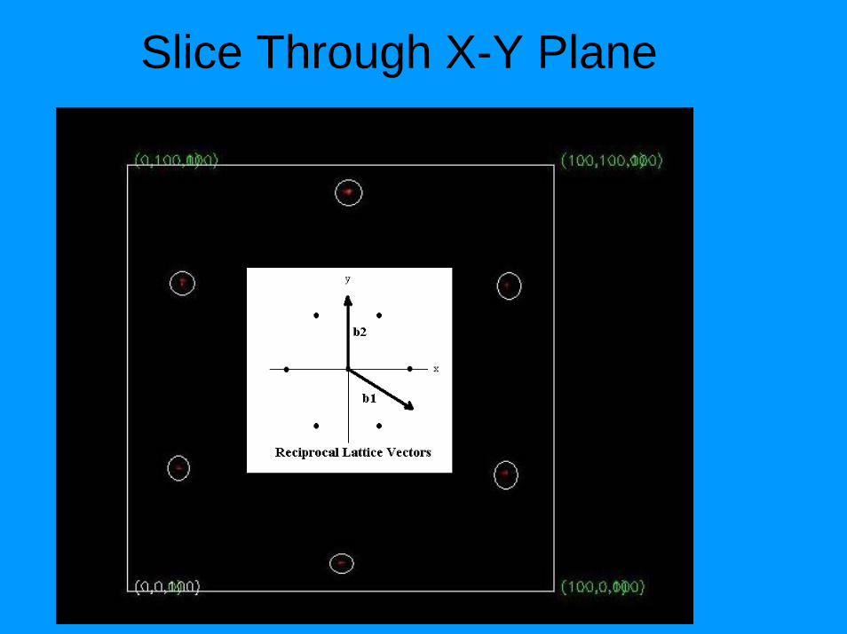
Slice Through X-Y Plane
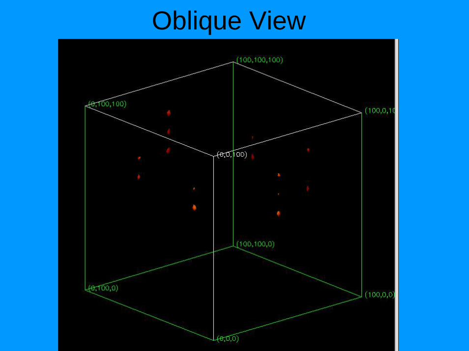
Oblique View
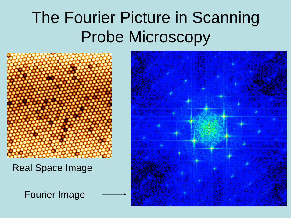
The Fourier Picture in Scanning Probe Microscopy
Real Space Image
Fourier Image
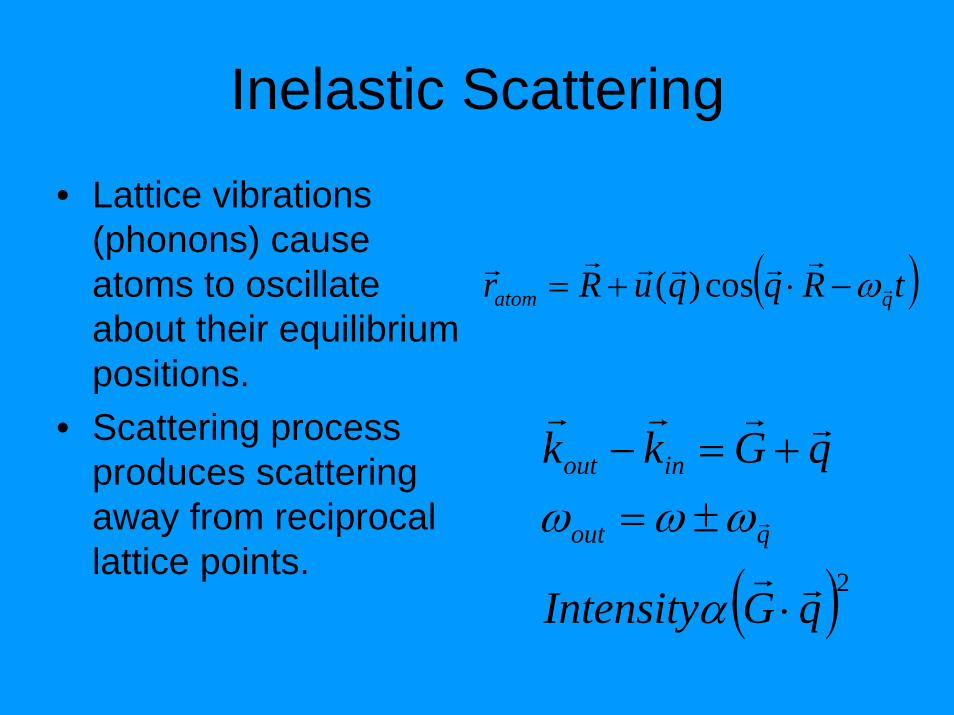
Inelastic Scattering
• Lattice vibrations (phonons) cause atoms to oscillate about their equilibrium positions.
• Scattering process produces scattering away from reciprocal lattice points.
( )tRqquRr qatom rrrrrrr ω−⋅+= cos)(
( )2qGIntensity
qGkk
qout
inout
rr
rrrr
r
⋅
±=+=−
α
ωωω
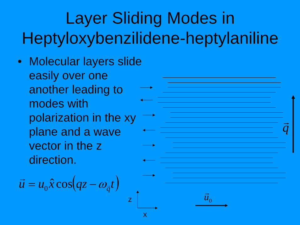
Layer Sliding Modes in Heptyloxybenzilidene-heptylaniline
• Molecular layers slide easily over one another leading to modes with polarization in the xyplane and a wave vector in the z direction.
qr
0ur( )tqzxuu qr
r ω−= cosˆ0
x
z
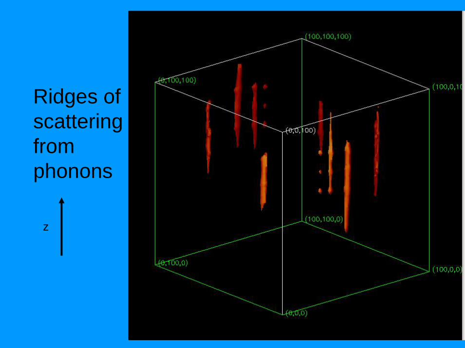
Ridges of scattering from phonons
z
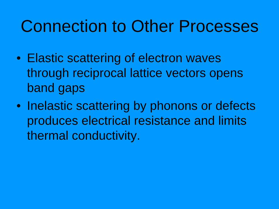
Connection to Other Processes
• Elastic scattering of electron waves through reciprocal lattice vectors opens band gaps
• Inelastic scattering by phonons or defects produces electrical resistance and limits thermal conductivity.
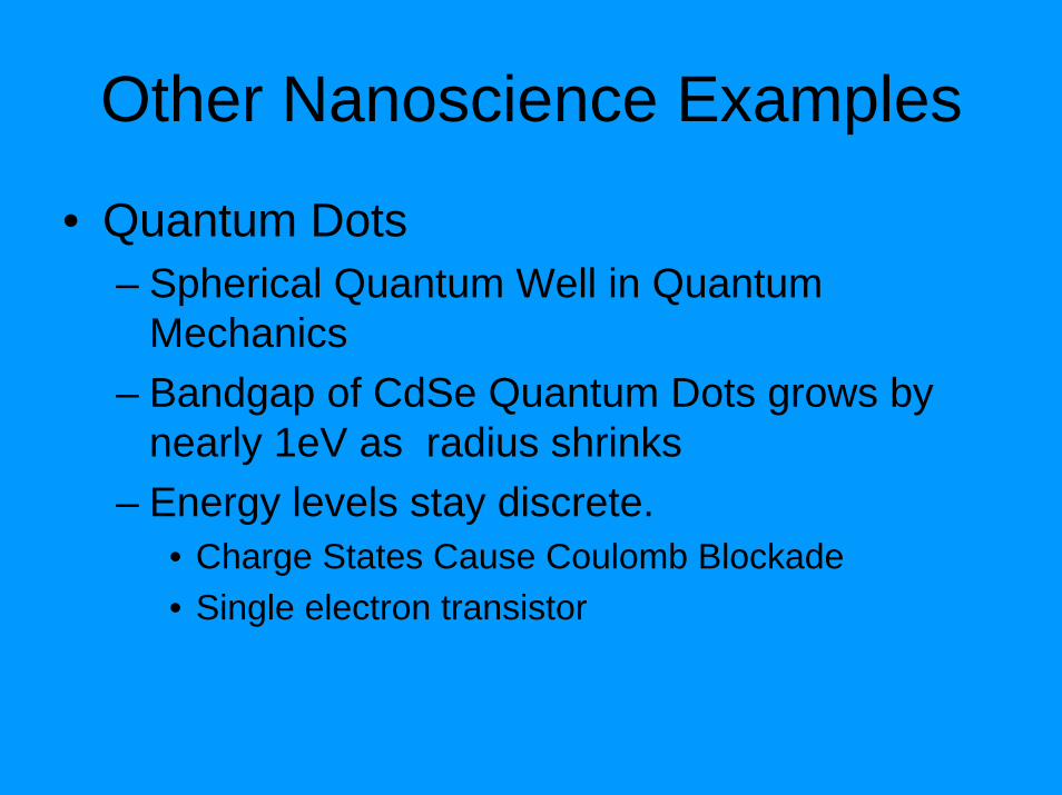
Other Nanoscience Examples
• Quantum Dots– Spherical Quantum Well in Quantum
Mechanics– Bandgap of CdSe Quantum Dots grows by
nearly 1eV as radius shrinks– Energy levels stay discrete.
• Charge States Cause Coulomb Blockade• Single electron transistor
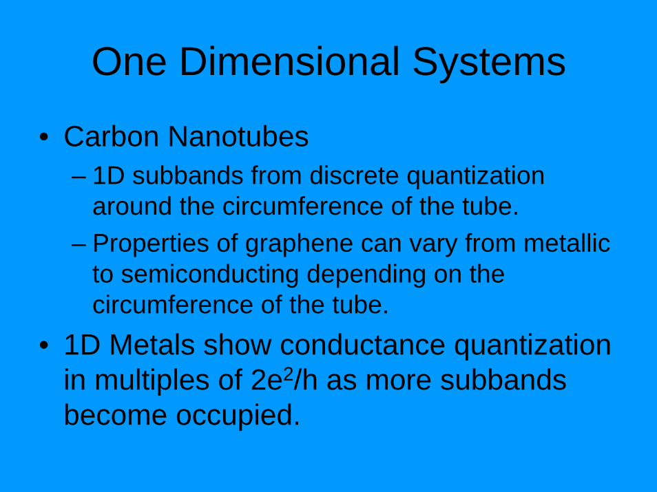
One Dimensional Systems
• Carbon Nanotubes– 1D subbands from discrete quantization
around the circumference of the tube.– Properties of graphene can vary from metallic
to semiconducting depending on the circumference of the tube.
• 1D Metals show conductance quantization in multiples of 2e2/h as more subbandsbecome occupied.
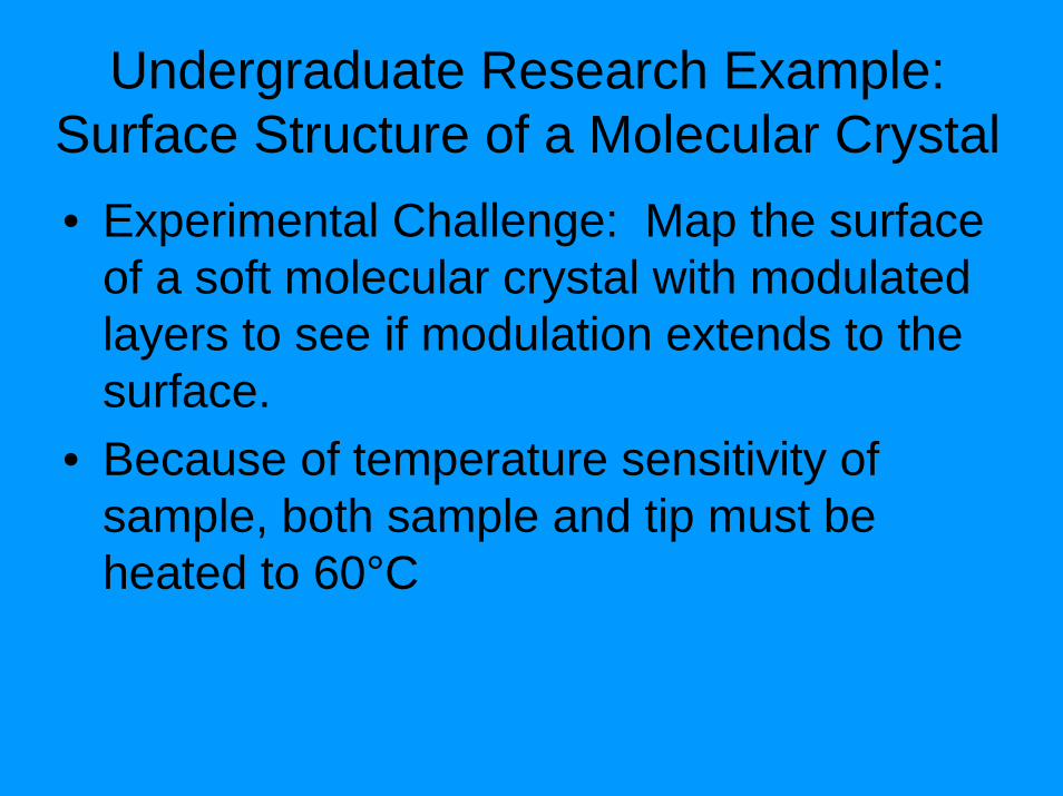
Undergraduate Research Example:Surface Structure of a Molecular Crystal• Experimental Challenge: Map the surface
of a soft molecular crystal with modulated layers to see if modulation extends to the surface.
• Because of temperature sensitivity of sample, both sample and tip must be heated to 60°C
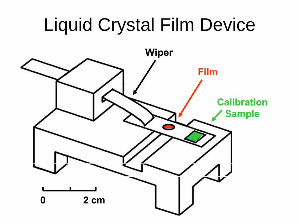
Liquid Crystal Film Device
Film
Wiper
0 2 cm
Calibration Sample
Film
Wiper
0 2 cm
Calibration Sample
Wiper
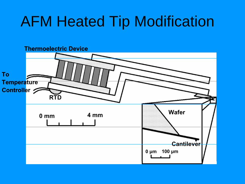
AFM Heated Tip ModificationThermoelectric Device
RTD
ToTemperatureController
Wafer
Cantilever
0 mm 4 mm
0 μm 100 μm
Thermoelectric Device
RTD
ToTemperatureController
Wafer
Cantilever
0 mm 4 mm
0 μm 100 μm
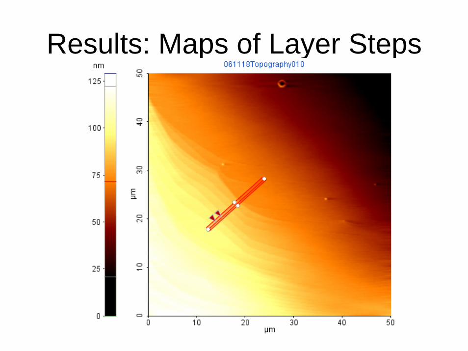
Results: Maps of Layer Steps
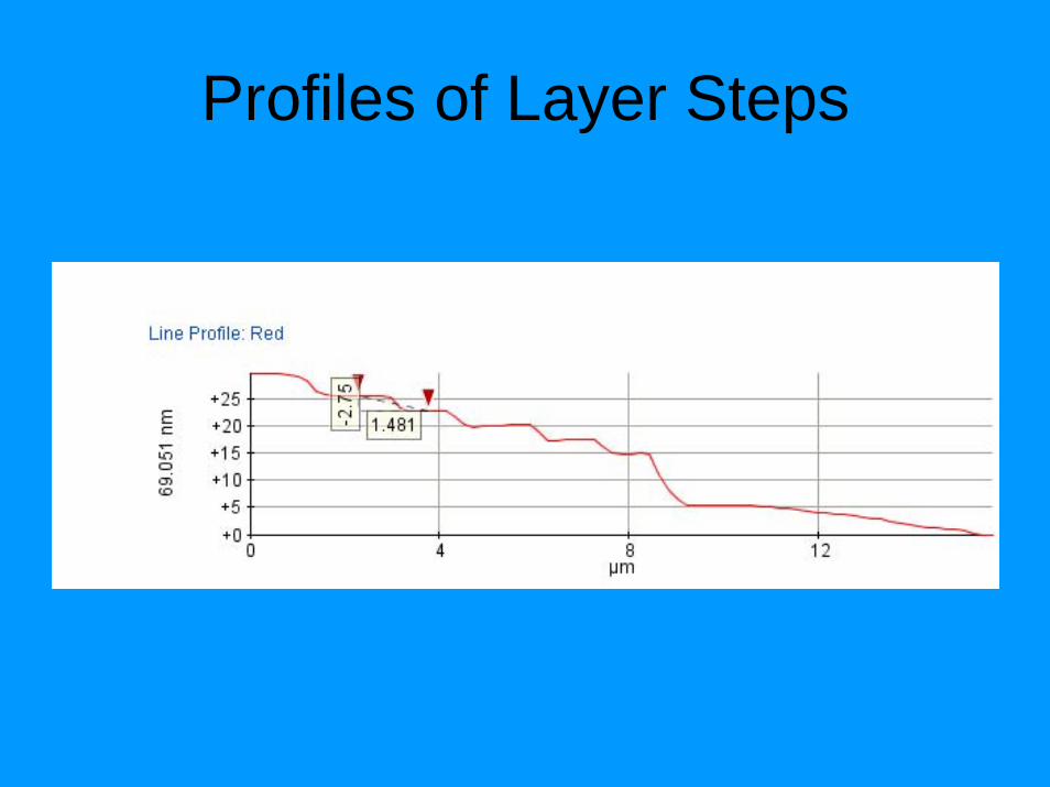
Profiles of Layer Steps
Conclusions
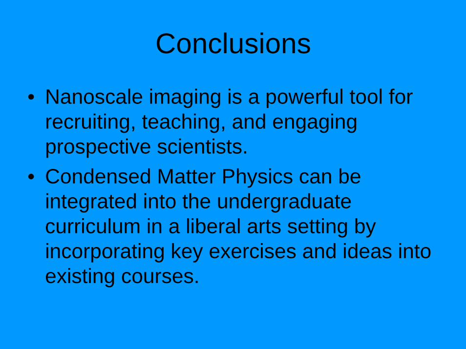
• Nanoscale imaging is a powerful tool for recruiting, teaching, and engaging prospective scientists.
• Condensed Matter Physics can be integrated into the undergraduate curriculum in a liberal arts setting by incorporating key exercises and ideas into existing courses.
Support
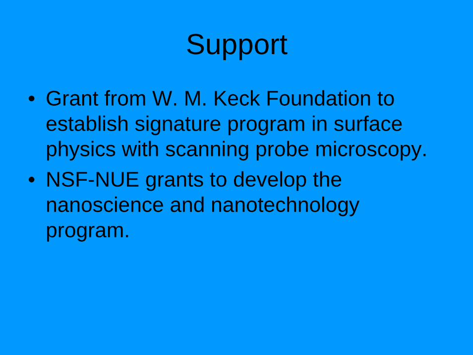
• Grant from W. M. Keck Foundation to establish signature program in surface physics with scanning probe microscopy.
• NSF-NUE grants to develop the nanoscience and nanotechnology program.