Embed Size (px)
Citation preview
National Tsing Hua University
CS4101 嵌入式系統概論
Introduction to LaunchPad
Prof. Chung-Ta KingDepartment of Computer Science
National Tsing Hua University, Taiwan
Materials from MSP430 Microcontroller Basics, John H. Davies, Newnes, 2008
National Tsing Hua University1
Outline
• MSP430 LaunchPad
• MSP430 Microcontroller
Processor
Memory
I/O
• First Program on LaunchPad
C
Assembly
• LaunchPad Development Environment
National Tsing Hua University2
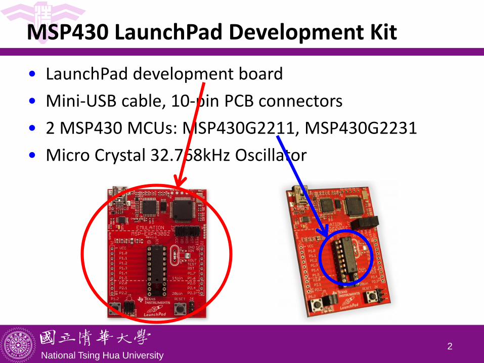
MSP430 LaunchPad Development Kit
• LaunchPad development board
• Mini-USB cable, 10-pin PCB connectors
• 2 MSP430 MCUs: MSP430G2211, MSP430G2231
• Micro Crystal 32.768kHz Oscillator
National Tsing Hua University3
MSP430 Microcontroller
• LaunchPad development kit uses microcontroller such as MSP430G2231
• Microcontroller:
A small computer on a single IC containing a processor core, memory, programmable I/O peripherals
• MSP430 microcontroller:
Incorporates a 16-bit RISC CPU, peripherals, and a flexible clock system that are interconnected using a von-Neumann common memory address bus (MAB) and memory data bus (MDB)
National Tsing Hua University4
MSP430 Microcontroller
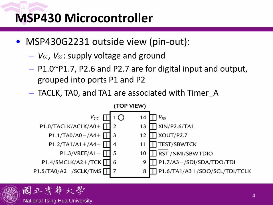
• MSP430G2231 outside view (pin-out):
VCC , VSS : supply voltage and ground
P1.0~P1.7, P2.6 and P2.7 are for digital input and output, grouped into ports P1 and P2
TACLK, TA0, and TA1 are associated with Timer_A
National Tsing Hua University5
MSP430 Microcontroller
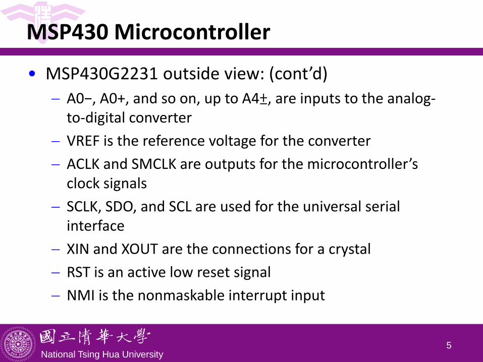
• MSP430G2231 outside view: (cont’d)
A0−, A0+, and so on, up to A4±, are inputs to the analog-to-digital converter
VREF is the reference voltage for the converter
ACLK and SMCLK are outputs for the microcontroller’s clock signals
SCLK, SDO, and SCL are used for the universal serial interface
XIN and XOUT are the connections for a crystal
RST is an active low reset signal
NMI is the nonmaskable interrupt input
National Tsing Hua University6
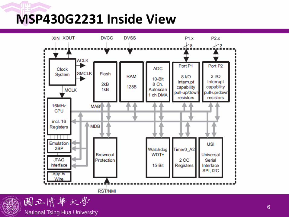
MSP430G2231 Inside View
National Tsing Hua University7
MSP430 CPU
• Instruction set architecture: RISC with 27 instructions and 7 addressing modes
16 16-bit registers with full register access including program counter, status registers, and stack pointer
Constant generator provides six most used immediate values and reduces code size
• Memory: Word and byte addressing and instruction formats
16-bit address bus allows direct access and branching throughout entire memory range
16-bit data bus allows direct manipulation of word-wide arguments
Direct memory-to-memory transfers without intermediate register holding
National Tsing Hua University8
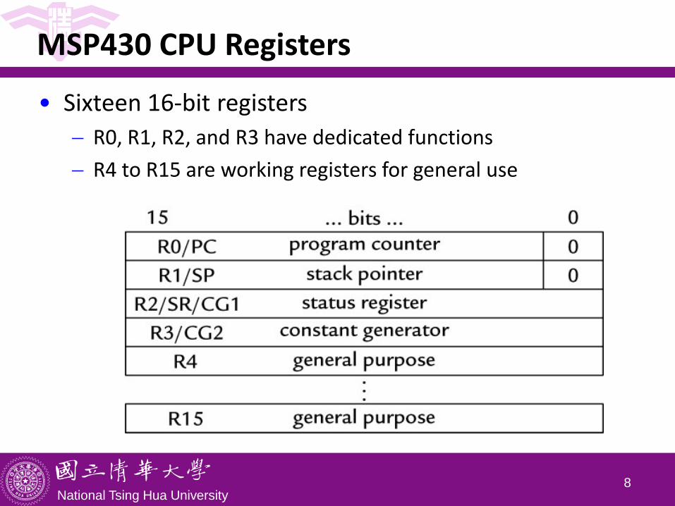
MSP430 CPU Registers
• Sixteen 16-bit registers
R0, R1, R2, and R3 have dedicated functions
R4 to R15 are working registers for general use
National Tsing Hua University9
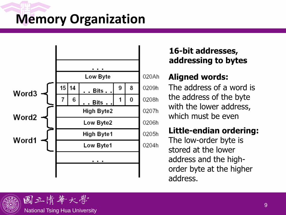
Memory Organization
Little-endian ordering: The low-order byte is stored at the lower address and the high-order byte at the higher address.
Aligned words:
The address of a word is the address of the byte with the lower address, which must be even
16-bit addresses, addressing to bytes
National Tsing Hua University10
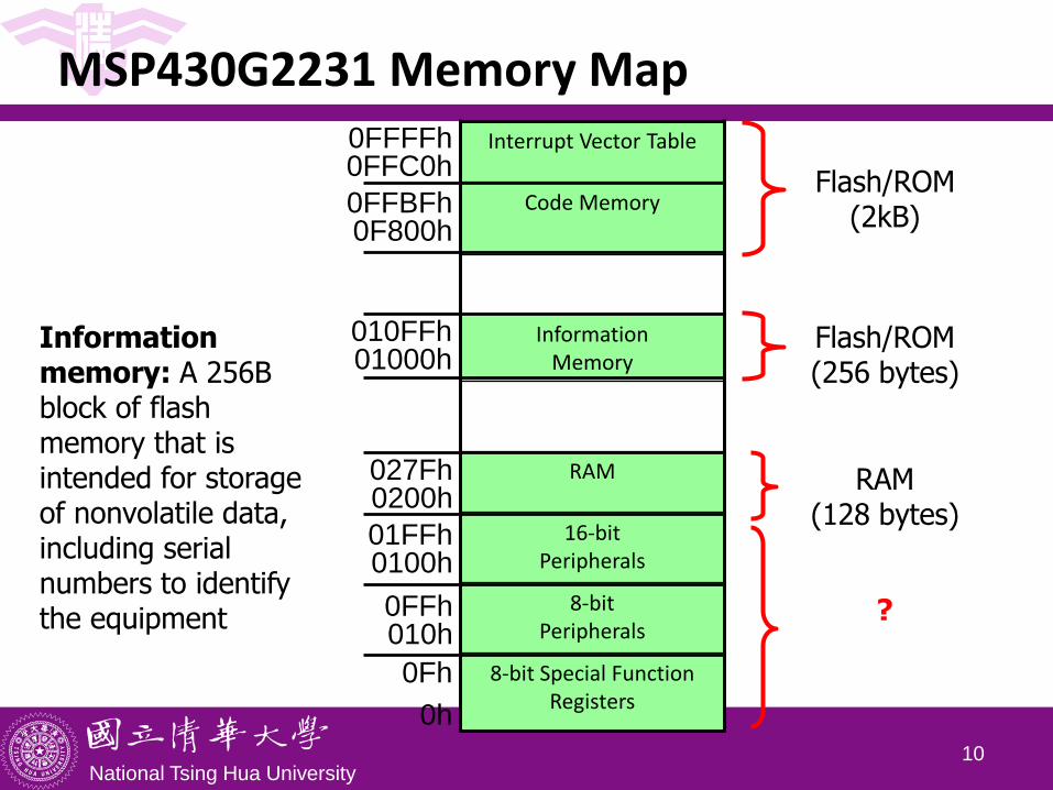
MSP430G2231 Memory MapInterrupt Vector Table
Code Memory
InformationMemory
RAM
16-bitPeripherals
8-bitPeripherals
8-bit Special FunctionRegisters
0Fh
0h
0FFh010h
01FFh0100h
027Fh0200h
0FFBFh0F800h
0FFFFh0FFC0h
010FFh01000h
Flash/ROM(2kB)
RAM(128 bytes)
Flash/ROM(256 bytes)
?
Information memory: A 256B block of flash memory that is intended for storage of nonvolatile data, including serial numbers to identify the equipment
National Tsing Hua University11
MSP430 Input/Output
• Simple digital input and output of MSP430 takes place through sets of pins on the package of the IC called ports
MSP430G2231 has two ports: P1 (8 bits: P1.0~P1.7), P2 (2 bits: P2.6~P2.7)
Typical pins can be configured for either input or output and some inputs may generate interrupts when the voltage on the pin changes
The ports appear to the CPU as registers (memory-mapped I/O ), each bit corresponds to a pin and a port may be associated to many registers for different purposes (next page)
National Tsing Hua University12
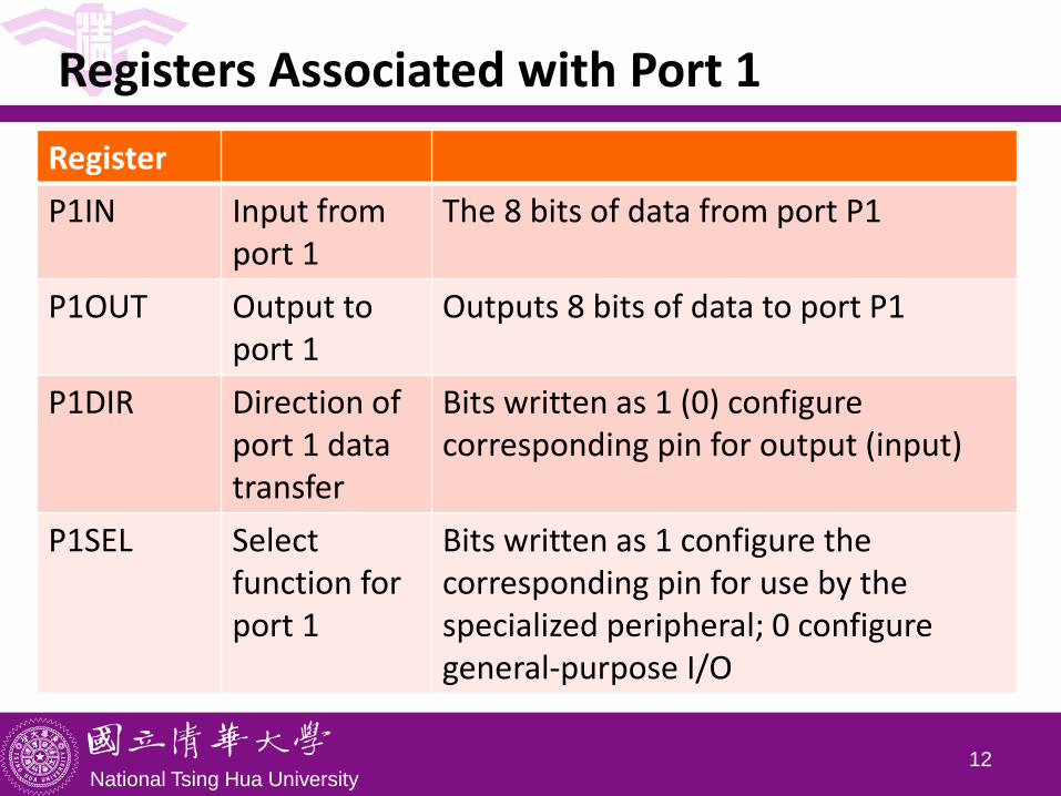
Registers Associated with Port 1
Register
P1IN Input from port 1
The 8 bits of data from port P1
P1OUT Output to port 1
Outputs 8 bits of data to port P1
P1DIR Direction of port 1 data transfer
Bits written as 1 (0) configure corresponding pin for output (input)
P1SEL Select function for port 1
Bits written as 1 configure the corresponding pin for use by the specialized peripheral; 0 configure general-purpose I/O
National Tsing Hua University13
Outline
• MSP430 LaunchPad
• MSP430 Microcontroller
Processor
Memory
I/O
• First Program on LaunchPad
C
Assembly
• LaunchPad Development Environment
National Tsing Hua University14
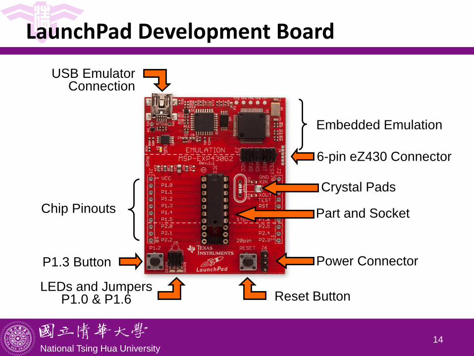
LaunchPad Development Board
Embedded Emulation
6-pin eZ430 Connector
Part and Socket
Crystal Pads
Power Connector
Reset ButtonLEDs and Jumpers
P1.0 & P1.6
P1.3 Button
Chip Pinouts
USB EmulatorConnection
National Tsing Hua University15
LaunchPad Pinouts
• On-board features of LaunchPad are pinned in the following fashion:
LED1 (red) = P1.0
LED2 (green) = P1.6
Switch1 = P1.3
Switch2 = Reset
Timer UART Transmit = P1.1
Timer UART Receive = P1.2
• In order to blink the Red and Green LEDs, we have to set Ports 1.0 and 1.6 as outputs, and toggle them
National Tsing Hua University16
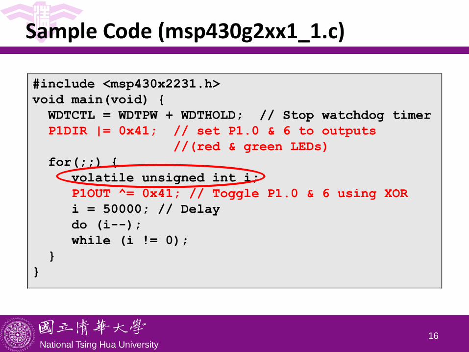
Sample Code (msp430g2xx1_1.c)
#include <msp430x2231.h>
void main(void) {
WDTCTL = WDTPW + WDTHOLD; // Stop watchdog timer
P1DIR |= 0x41; // set P1.0 & 6 to outputs
//(red & green LEDs)
for(;;) {
volatile unsigned int i;
P1OUT ^= 0x41; // Toggle P1.0 & 6 using XOR
i = 50000; // Delay
do (i--);
while (i != 0);
}
}
National Tsing Hua University17
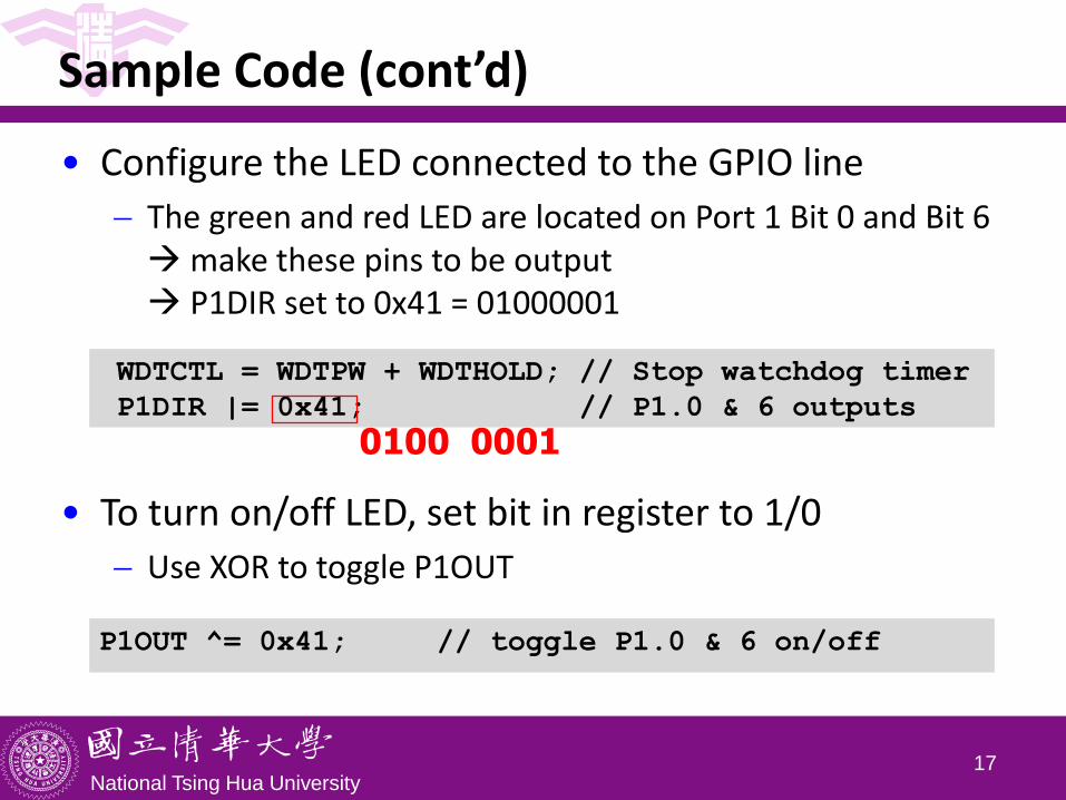
Sample Code (cont’d)
• Configure the LED connected to the GPIO line
The green and red LED are located on Port 1 Bit 0 and Bit 6 make these pins to be output P1DIR set to 0x41 = 01000001
• To turn on/off LED, set bit in register to 1/0
Use XOR to toggle P1OUT
P1OUT ^= 0x41; // toggle P1.0 & 6 on/off
WDTCTL = WDTPW + WDTHOLD; // Stop watchdog timer
P1DIR |= 0x41; // P1.0 & 6 outputs
0100 0001
National Tsing Hua University18
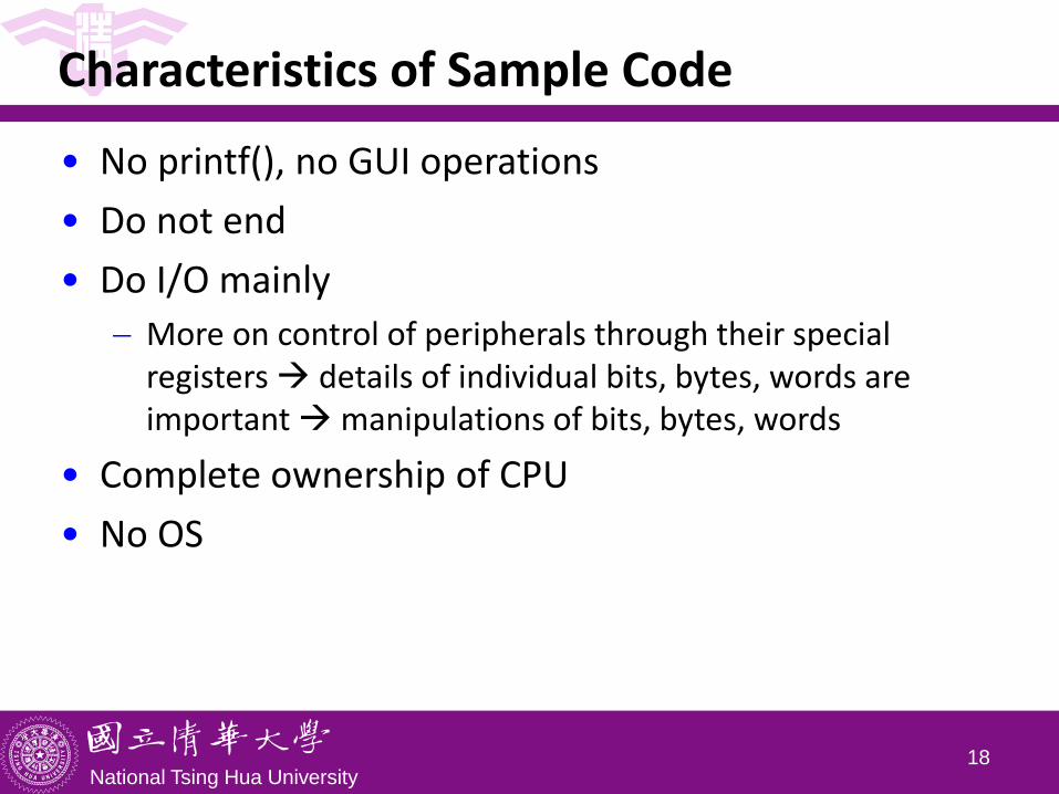
Characteristics of Sample Code
• No printf(), no GUI operations
• Do not end
• Do I/O mainly
More on control of peripherals through their special registers details of individual bits, bytes, words are important manipulations of bits, bytes, words
• Complete ownership of CPU
• No OS
National Tsing Hua University19
Notes of Sample Code
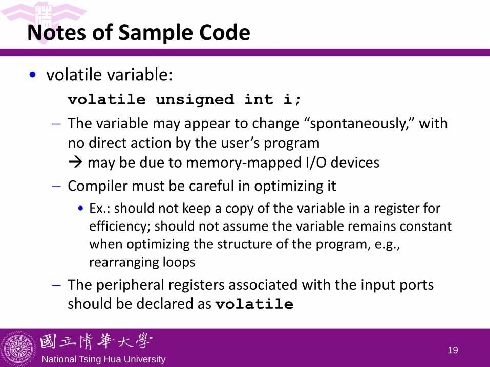
• volatile variable:volatile unsigned int i;
The variable may appear to change “spontaneously,” with no direct action by the user’s programmay be due to memory-mapped I/O devices
Compiler must be careful in optimizing it
• Ex.: should not keep a copy of the variable in a register for efficiency; should not assume the variable remains constant when optimizing the structure of the program, e.g., rearranging loops
The peripheral registers associated with the input ports should be declared as volatile
National Tsing Hua University20
Notes of Sample Code
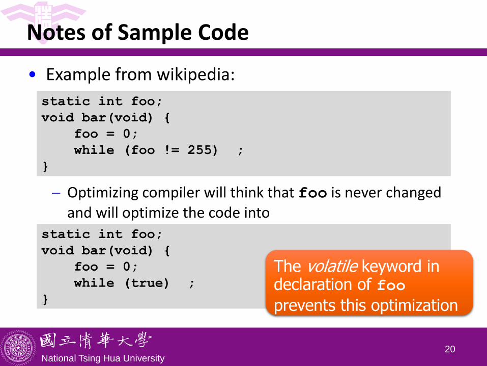
• Example from wikipedia:
Optimizing compiler will think that foo is never changed and will optimize the code into
static int foo;
void bar(void) {
foo = 0;
while (foo != 255) ;
}
static int foo;
void bar(void) {
foo = 0;
while (true) ;
}
The volatile keyword in declaration of foo
prevents this optimization
National Tsing Hua University21
Notes of Sample Code
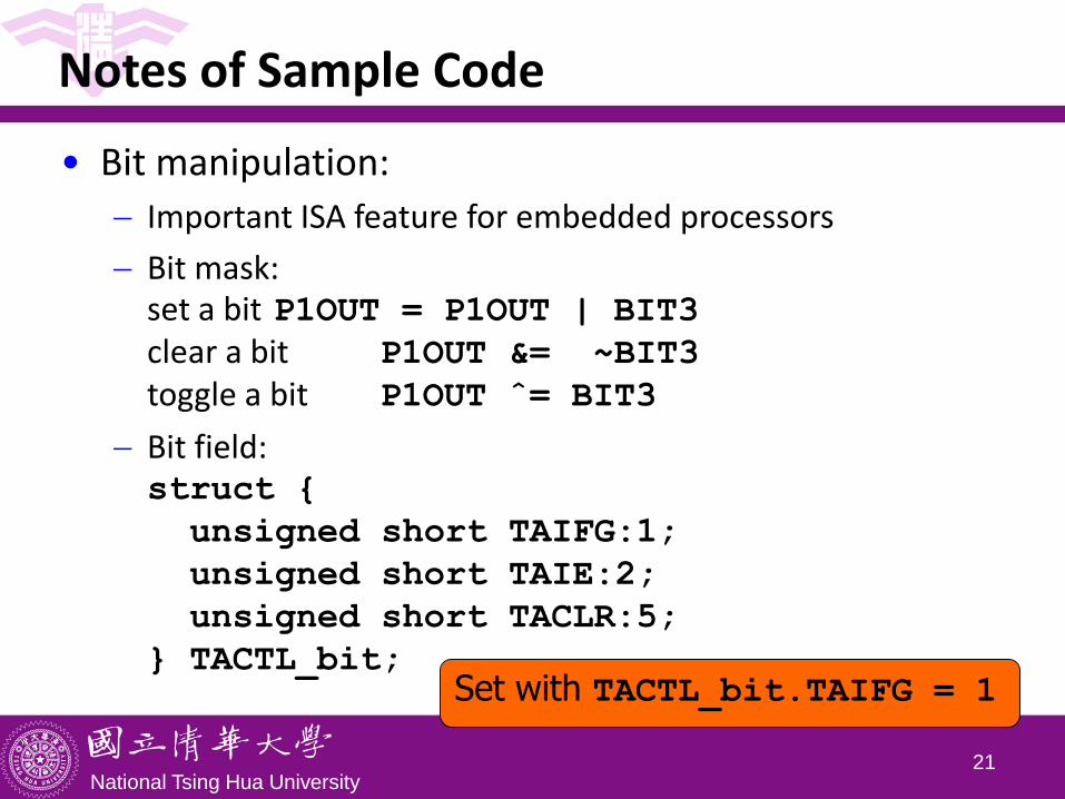
• Bit manipulation:
Important ISA feature for embedded processors
Bit mask:set a bit P1OUT = P1OUT | BIT3clear a bit P1OUT &= ~BIT3
toggle a bit P1OUT ˆ= BIT3
Bit field:struct {
unsigned short TAIFG:1;
unsigned short TAIE:2;
unsigned short TACLR:5;
} TACTL_bit;Set with TACTL_bit.TAIFG = 1
National Tsing Hua University22
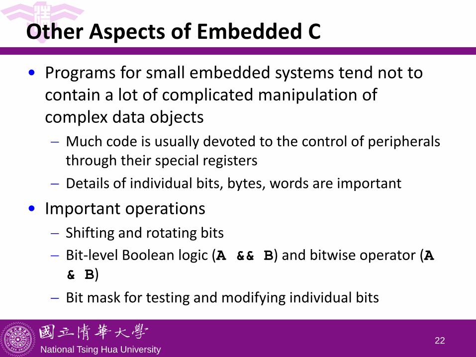
Other Aspects of Embedded C
• Programs for small embedded systems tend not to contain a lot of complicated manipulation of complex data objects
Much code is usually devoted to the control of peripherals through their special registers
Details of individual bits, bytes, words are important
• Important operations
Shifting and rotating bits
Bit-level Boolean logic (A && B) and bitwise operator (A & B)
Bit mask for testing and modifying individual bits
National Tsing Hua University23
Other Aspects of Embedded C
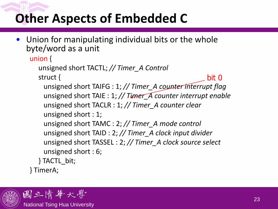
• Union for manipulating individual bits or the whole byte/word as a unitunion {
unsigned short TACTL; // Timer_A Controlstruct {
unsigned short TAIFG : 1; // Timer_A counter interrupt flagunsigned short TAIE : 1; // Timer_A counter interrupt enableunsigned short TACLR : 1; // Timer_A counter clearunsigned short : 1;unsigned short TAMC : 2; // Timer_A mode controlunsigned short TAID : 2; // Timer_A clock input dividerunsigned short TASSEL : 2; // Timer_A clock source selectunsigned short : 6;
} TACTL_bit;} TimerA;
bit 0
National Tsing Hua University24
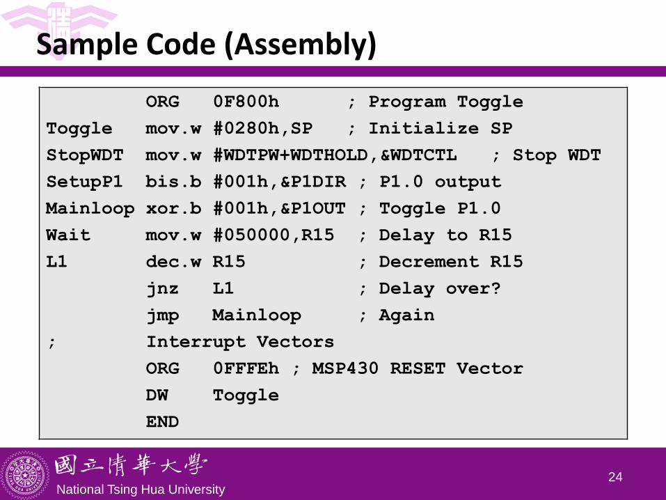
Sample Code (Assembly)
ORG 0F800h ; Program Toggle
Toggle mov.w #0280h,SP ; Initialize SP
StopWDT mov.w #WDTPW+WDTHOLD,&WDTCTL ; Stop WDT
SetupP1 bis.b #001h,&P1DIR ; P1.0 output
Mainloop xor.b #001h,&P1OUT ; Toggle P1.0
Wait mov.w #050000,R15 ; Delay to R15
L1 dec.w R15 ; Decrement R15
jnz L1 ; Delay over?
jmp Mainloop ; Again
; Interrupt Vectors
ORG 0FFFEh ; MSP430 RESET Vector
DW Toggle
END
National Tsing Hua University25
Notes of Assembly Code
• Where to store the program in memory? The code should go into the flash ROM and variables should be
allocated in RAM
code at start of flash: 0F800h
stack at end of RAM: 0280h
• Where should execution of the program start? Address of the first instruction to be executed is stored at a specific
location in flash, called reset vector, which occupies the 2 bytes at 0FFFEh:0FFFFh
Use an ORG 0xFFFE directive to tell the assembler where to store the reset vector
The DW directive (“define word”) tells the assembler to store the following word (2 bytes) in memory
National Tsing Hua University26
Notes of Assembly Code
• The style of program shown above is known as absolute assembly because the memory addresses are given explicitly in the source using ORG directives
• An alternative is to rely on the linker/loader to determine the address, which is called relocatable assembly
The program must not contain absolute addresses, e.g., jump to a 16-bit address, only relative addresses, e.g., relative to current program counter
National Tsing Hua University27
Outline
• MSP430 LaunchPad
• MSP430 Microcontroller
Processor
Memory
I/O
• First Program on LaunchPad
C
Assembly
• LaunchPad Development Environment
National Tsing Hua University
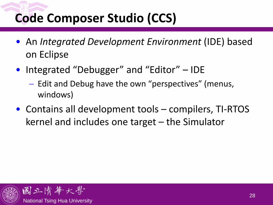
Code Composer Studio (CCS)
• An Integrated Development Environment (IDE) based on Eclipse
• Integrated “Debugger” and “Editor” – IDE
Edit and Debug have the own “perspectives” (menus, windows)
• Contains all development tools – compilers, TI-RTOS kernel and includes one target – the Simulator
28
National Tsing Hua University
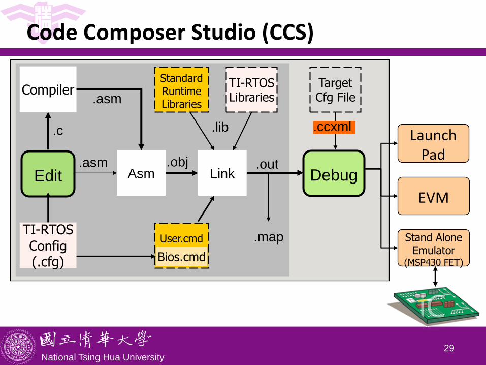
Code Composer Studio (CCS)
29
Compiler
Asm
.c
.asm .obj
.asm
Edit Debug
Standard Runtime Libraries
.out
.lib
.mapUser.cmd
TI-RTOSLibraries
TI-RTOSConfig(.cfg) Bios.cmd
Launch Pad
EVM
Stand Alone Emulator
(MSP430 FET)
TargetCfg File
.ccxml
Link
National Tsing Hua University
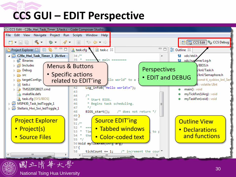
CCS GUI – EDIT Perspective
30
Project Explorer
• Project(s)
• Source Files
Source EDIT’ing
• Tabbed windows
• Color-coded text
Outline View
• Declarations and functions
Menus & Buttons
• Specific actions related to EDIT’ing
Perspectives
• EDIT and DEBUG
National Tsing Hua University
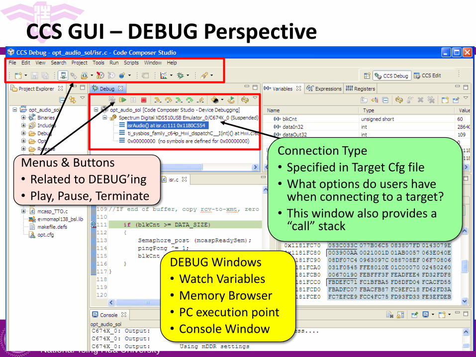
CCS GUI – DEBUG Perspective
31
DEBUG Windows
• Watch Variables
• Memory Browser
• PC execution point
• Console Window
Menus & Buttons
• Related to DEBUG’ing
• Play, Pause, Terminate
Connection Type
• Specified in Target Cfg file
• What options do users have when connecting to a target?
• This window also provides a “call” stack
National Tsing Hua University32
Notes on Code Composer Studio
• Download code to LaunchPad from CCS
After application program is entered and all the changes are made, we can download this code to the MSP430 MCU plugged into LaunchPad’s DIP target socket
Make sure LaunchPad is plugged in to your PC
Next, click the “Debug” button, which will check the code and load it into the MSP430 device
When the code successfully loads, we will enter the Debug view of CCS. We can execute the code by clicking the green “Run” arrow and start debugging
National Tsing Hua University33
Summary
• Basic structure of MSP430 LaunchPad:
MSP430 CPU and memory
MSP430 I/O ports and LaunchPad I/O connections
• First MSP430 program
C and assembly
Importance of bit/byte manipulation
Management and allocation of memory
![Vortrag zur Seminarphase der PG „Solar Doorplate“ MSP430 ... · MSP430 – Wichtigste Grundlagen von David Tondorf. 2 ... MSP430 microcontroller basics. Oxford: Newnes [4] MSP430](https://img.pdfslide.tips/doc/110x75/5b6f6a9b7f8b9af12d8c481e/vortrag-zur-seminarphase-der-pg-solar-doorplate-msp430-msp430-.jpg)


![[MSP430] ADC10](https://img.pdfslide.tips/doc/110x75/55cf97c5550346d033938430/msp430-adc10-5654b9a37ede3.jpg)
![[MSP430] GPIO](https://img.pdfslide.tips/doc/110x75/55cf9df0550346d033aff200/msp430-gpio.jpg)