Embed Size (px)
Citation preview
MS415 Lec. 11
• Instructor: Prof. Keon Jae Lee
- Office: 응용공학동 #4306, Tel: #3343
- Email: [email protected]
- Office hour: 9:00-10:20 (Mon, Wed),
Introduction to Semiconductor Devices (MS 415)
Course Policies:• Attendance: Two uninformed absences are allowed and will not be used for grades. However, after third absence, grade will be affected. Late attendance will be considered as absence.
• Assignments: All assignments (~8 HWs) need to be submitted on the due date. Otherwise, a penalty can be considered for each assignment.
• Undergraduate and graduate students will be evaluated separately.
Education Values: Accountability, Professionalism, Work Ethics
Objective:The objective of this course is to teach the physical operating mechanism of semiconductor devices; carrier transport in semiconductor, p-n junction, metal/semiconductor junction, MOS capacitor, bipolar junction transistor, MESFET and MOSFET.
• Grading: Midterm 30%,
Final 40%,
HW 20%,
Attendance 10%
• Assistant: Kyung Chul Park (박경철)
- Office: 응용공학동 #4301, Tel: #3383
- Email: [email protected]
• Lecture: Mon, Wed 10:30-11:45 #1317
• Textbook: Solid State Electronic Devices,
7th Edition, B. G. Streetman, Prentice Hall
MS415 Lec. 12
Introduction to Semiconductor Devices (MS 415)
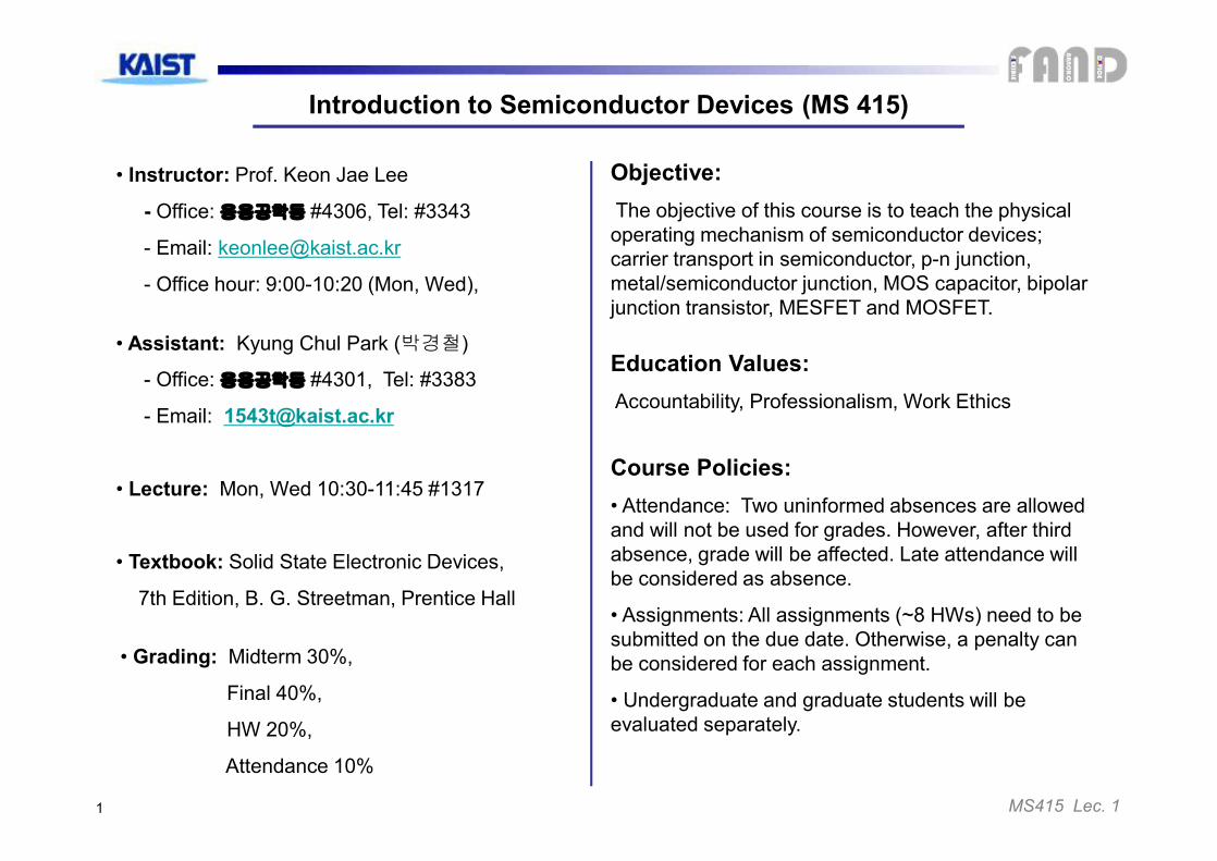
Week Topic Text
9 Breakdown MechanismMetal/Semiconductor contact
Chap 5
10 MOS Capacitor Threshold voltage & CV characteristics
Chap 6
11 MOS Field Effect Transistors: Basic Operation
Chap 6
12 MOS Field Effect Transistors: Current-Voltage Characteristics
Chap 6
13 Bipolar Junction Transistors: Amplifying Characteristics
Chap 7
14 Modern MOSFET, MESFET Optoelectronic devices
Chap 6Chap 8
15 Integrated Circuits:CMOS Process Integration, Logic and Memory Devices
Chap 9
16 ReviewFinal exam
Home Page:http://fand.kaist.ac.kr/Lecture.htm (PasswordàMS415)
• Course Schedule
Week Topic Text
1 Introduction to Semiconductor Devices; Overview, history, industry and market
2 Crystal propertiesAtom, Electron and Schrodinger Wave Equation
Chap 1Chap 2
3 Carriers in SemiconductorsCarrier Concentrations
Chap 3
4 Drift of Carriers in Electric & Magnetic FieldExcess Carriers Gen. and Recom & Quasi-Fermi Level
Chap 3Chap 4
5 Carrier Transport: Drift & DiffusionPN Junction under Equilibrium
Chap 4
6 PN Junction under Equilibrium Space Charge & Depletion Regions
Chap 5
7 PN Junction Current Eq. Capacitance of PN Junction
Chap 5
8 Review Mid-term
MS415 Lec. 13
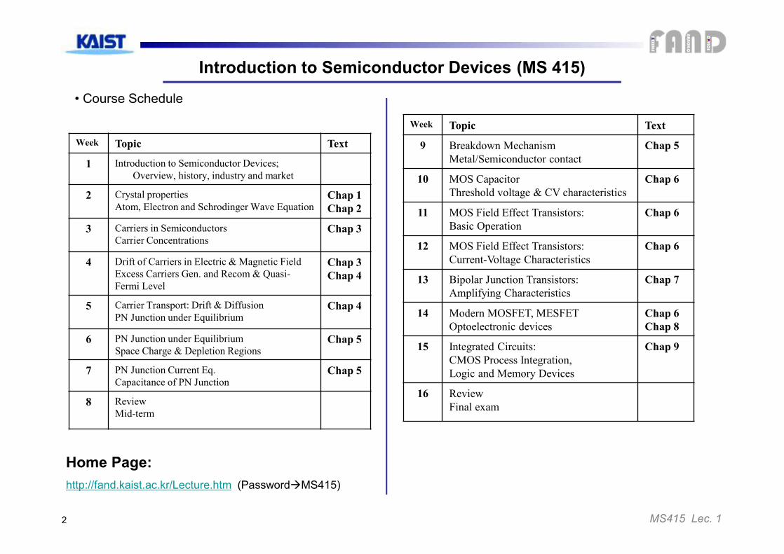
Course Overview
Metal-Oxide-Semiconductor Field Effect Transistors
(MOSFET)
Course overview: theoretical understanding and calculation (No prerequisite)
Midterm: Crystal property, Carriers in Semiconductor,
Carrier Transport, PN junction,
Final: Metal/Semiconductor junction, MOS CV,
MOSFET, BJT and other electronic devices
Next level device class: Semiconductor Integrated Process Design (MS635, Fall 2018, Prof. K. Lee)
à Practical and terminology oriented class, less calculation, modern MOSFET, state of art VLSI technology
Related class: Quantum Mechanics, Solid State Physics
Crystallography, Semiconductor Process
Switch on/off by modulating gate voltage
Source electrode (Gnd)
Gate electrode
Drain electrode (5V)
p-type Si substrate
Source (n+) Drain (n+)
Gate
Gate oxide
MOSFET
Vg > Vth >0 Tr is on
Vg =0 Tr is off
MS415 Lec. 14
History of Semiconductors
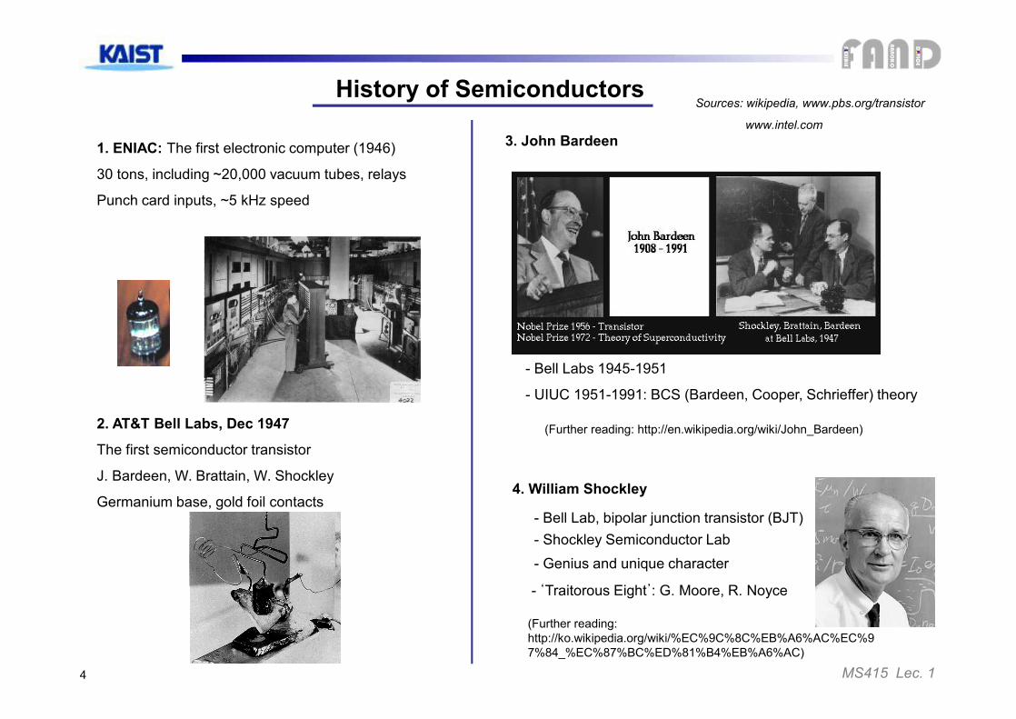
1. ENIAC: The first electronic computer (1946)
30 tons, including ~20,000 vacuum tubes, relays
Punch card inputs, ~5 kHz speed
2. AT&T Bell Labs, Dec 1947
The first semiconductor transistor
J. Bardeen, W. Brattain, W. Shockley
Germanium base, gold foil contacts
- Bell Labs 1945-1951
- UIUC 1951-1991: BCS (Bardeen, Cooper, Schrieffer) theory
3. John Bardeen
4. William Shockley
- Bell Lab, bipolar junction transistor (BJT)
- Genius and unique character
(Further reading: http://en.wikipedia.org/wiki/John_Bardeen)
(Further reading: http://ko.wikipedia.org/wiki/%EC%9C%8C%EB%A6%AC%EC%97%84_%EC%87%BC%ED%81%B4%EB%A6%AC)
- Shockley Semiconductor Lab
Sources: wikipedia, www.pbs.org/transistor
www.intel.com
- ‘Traitorous Eight’: G. Moore, R. Noyce
MS415 Lec. 15
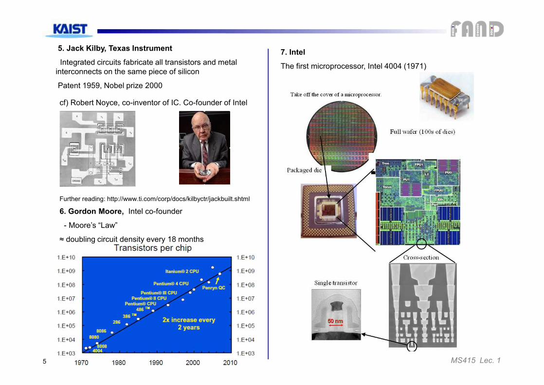
5. Jack Kilby, Texas Instrument
Integrated circuits fabricate all transistors and metal interconnects on the same piece of silicon
Patent 1959, Nobel prize 2000
7. Intel
The first microprocessor, Intel 4004 (1971)
cf) Robert Noyce, co-inventor of IC. Co-founder of Intel
Further reading: http://www.ti.com/corp/docs/kilbyctr/jackbuilt.shtml
6. Gordon Moore, Intel co-founder
- Moore’s “Law”
≈ doubling circuit density every 18 months

MS415 Lec. 16
Transistor scaling and power consumption
Hot Plate
Nuclear ReactorRocket Nozzle
10. Fujio Masuoka. Toshiba,
Further reading: http://www.forbes.com/global/2002/0624/030_print.html
- The first invention of both NOR & NAND Flash memory (1980)
- Ubiquitous electronic devices
(Cell phone, ipod, digital camera, SSD)
11. Nick Holonyak, GE & Shuji Nakamura, Nichia- The first invention of LED (N.H. 1962) & blue GaN LED (S.N., 1993)
- N.H is the first Ph.D student of Bardeen.
- S.N. sued Nichia and won ~$180 million (2000억).
But settled at $ 7 million after appeal
8. Robert Dennard, IBM T.J Watson
- The invention of DRAM, 1966
- Formulated “Scaling Theory”
9. Dawon Kahng, Martin, Atalla, Bell labs.
- The first invention of MOSFETs, 1960
- Floating Gate non-volatile memory, 1967
MS415 Lec. 17
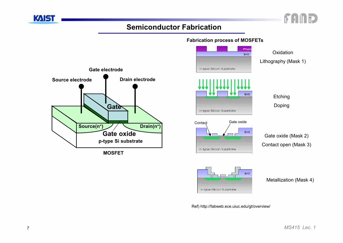
Fabrication process of MOSFETs
Oxidation
Lithography (Mask 1)
Etching
Doping
Gate oxide (Mask 2)
Contact open (Mask 3)
Metallization (Mask 4)
Ref) http://fabweb.ece.uiuc.edu/gt/overview/
Semiconductor Fabrication
Gate oxide Contact
Source electrode
Gate electrode
Drain electrode
p-type Si substrate
Source(n+) Drain(n+)
Gate
Gate oxide
MOSFET
MS415 Lec. 18
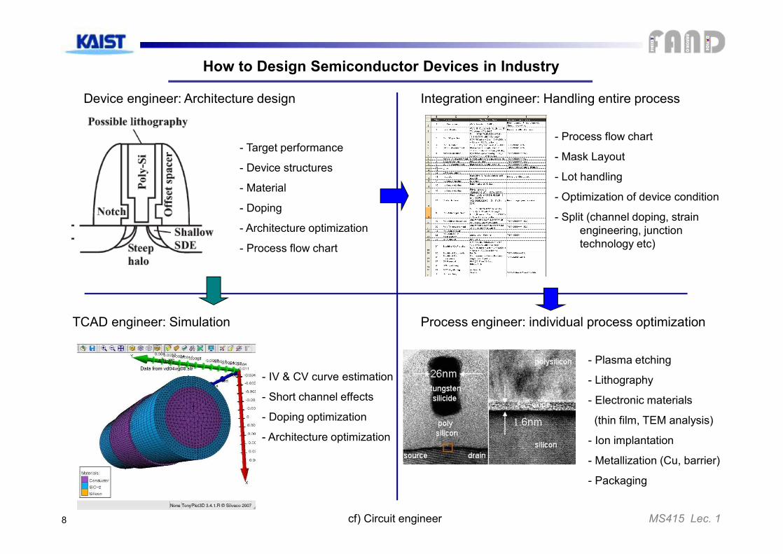
How to Design Semiconductor Devices in Industry
Device engineer: Architecture design Integration engineer: Handling entire process
Process engineer: individual process optimization
- Target performance
- Device structures
- Material
- Doping
- Architecture optimization
- Process flow chart
- IV & CV curve estimation
- Short channel effects
- Doping optimization
- Architecture optimization
- Plasma etching
- Lithography
- Electronic materials
(thin film, TEM analysis)
- Ion implantation
- Metallization (Cu, barrier)
- Packaging
- Process flow chart
- Mask Layout
- Lot handling
- Optimization of device condition
- Split (channel doping, strain engineering, junction technology etc)
TCAD engineer: Simulation
cf) Circuit engineer
MS415 Lec. 19
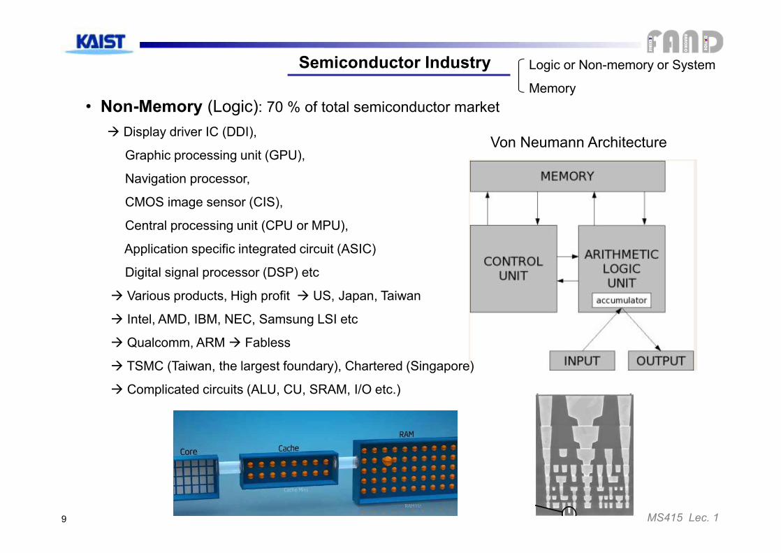
Semiconductor Industry
Von Neumann Architecture
• Non-Memory (Logic): 70 % of total semiconductor marketà Display driver IC (DDI),
Graphic processing unit (GPU),
Navigation processor,
CMOS image sensor (CIS),
Central processing unit (CPU or MPU),
Application specific integrated circuit (ASIC)
Digital signal processor (DSP) etc
à Various products, High profit à US, Japan, Taiwan
à Intel, AMD, IBM, NEC, Samsung LSI etc
à Qualcomm, ARM à Fabless
à TSMC (Taiwan, the largest foundary), Chartered (Singapore)
à Complicated circuits (ALU, CU, SRAM, I/O etc.)
Logic or Non-memory or System
Memory
MS415 Lec. 110
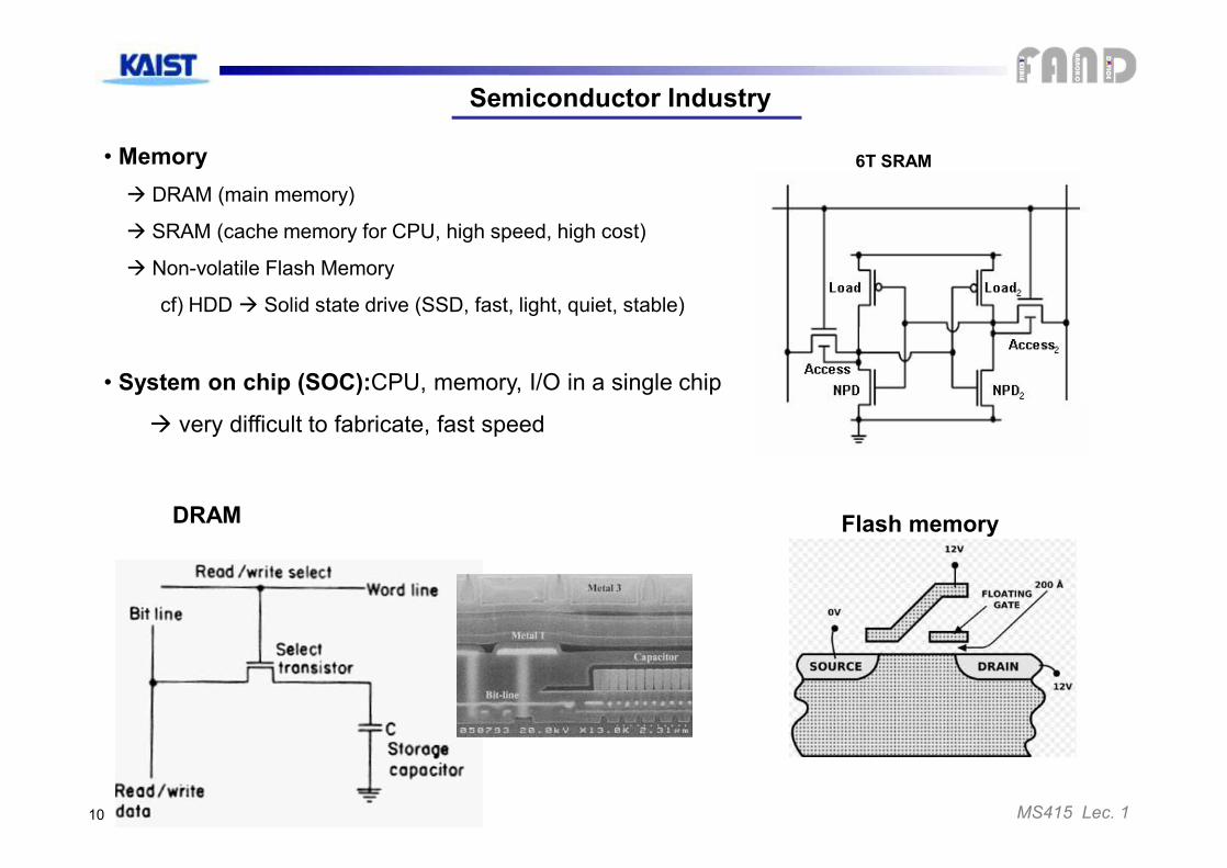
Semiconductor Industry
6T SRAM
DRAM
• Memory à DRAM (main memory)
à SRAM (cache memory for CPU, high speed, high cost)
à Non-volatile Flash Memory
cf) HDD à Solid state drive (SSD, fast, light, quiet, stable)
• System on chip (SOC):CPU, memory, I/O in a single chip
à very difficult to fabricate, fast speed
Flash memory
MS415 Lec. 111
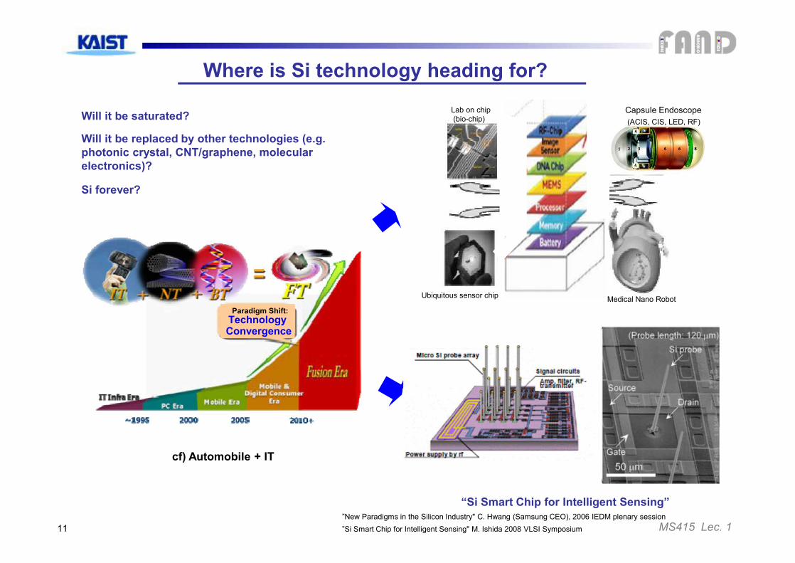
Where is Si technology heading for?
Paradigm Shift:TechnologyConvergence
Will it be saturated?
Will it be replaced by other technologies (e.g. photonic crystal, CNT/graphene, molecular electronics)?
Lab on chip(bio-chip)
RF chip
Image sensor
MPU
Memory
Battery
MEMs
Ubiquitous sensor chip Medical Nano Robot
DNA chips
Capsule Endoscope(ACIS, CIS, LED, RF)
Si forever?
“Si Smart Chip for Intelligent Sensing”
cf) Automobile + IT
”New Paradigms in the Silicon Industry" C. Hwang (Samsung CEO), 2006 IEDM plenary session”Si Smart Chip for Intelligent Sensing" M. Ishida 2008 VLSI Symposium
MS415 Lec. 112
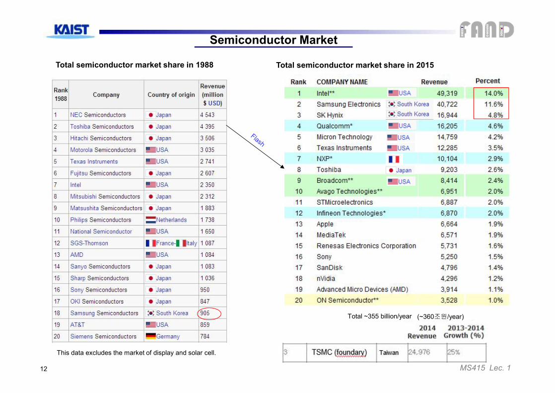
Total semiconductor market share in 2015Total semiconductor market share in 1988
Semiconductor Market
This data excludes the market of display and solar cell.
(~360조원/year)Total ~355 billion/year
MS415 Lec. 1
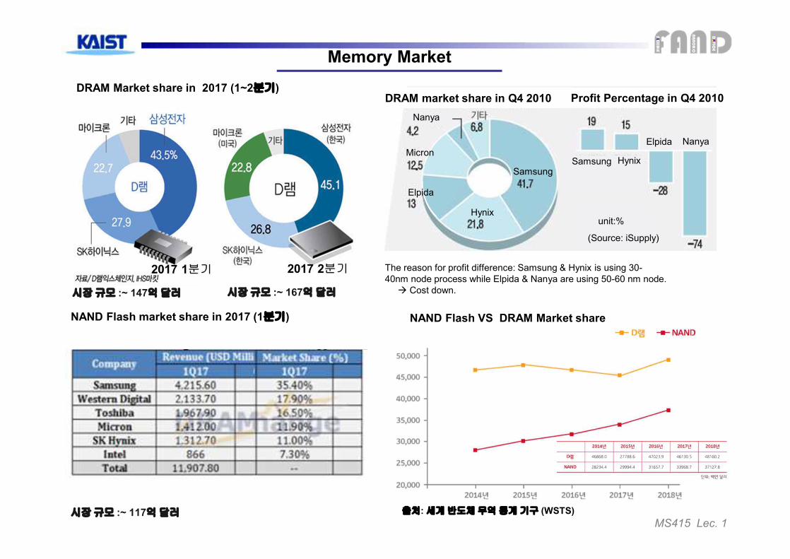
DRAM Market share in 2017 (1~2분기)
Memory Market
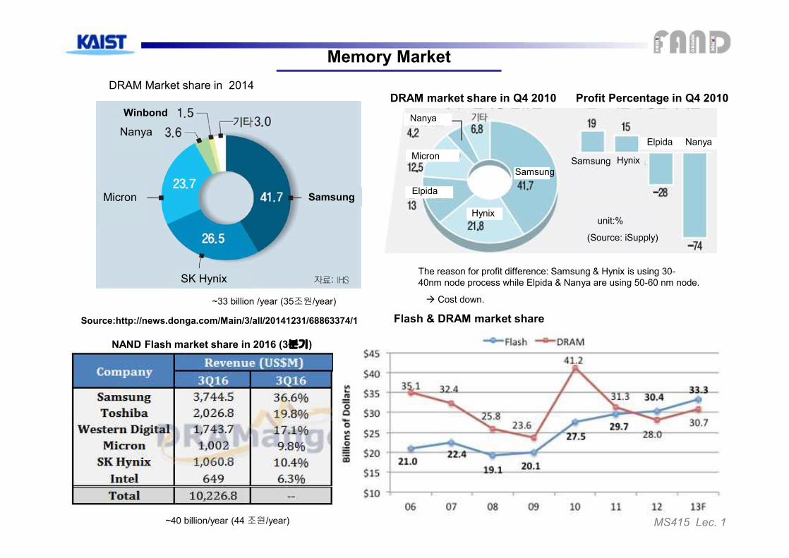
The reason for profit difference: Samsung & Hynix is using 30-40nm node process while Elpida & Nanya are using 50-60 nm node.
à Cost down.
DRAM market share in Q4 2010
Samsung
unit:%
(Source: iSupply)
Hynix
Nanya
HynixSamsung
Elpida Nanya
DRAM market share in Q4 2010DRAM market share in Q4 2010 Profit Percentage in Q4 2010
2012 2012
NAND Flash market share in 2017 (1분기) NAND Flash VS DRAM Market share
출처: 세계반도체무역통계기구 (WSTS)
시장규모 :~ 147억달러 시장규모 :~ 167억달러
시장규모 :~ 117억달러
Elpida
Micron
MS415 Lec. 1
NAND Flash market share in 2016 (3분기)
DRAM Market share in 2014
~33 billion /year (35조원/year)
~40 billion/year (44 조원/year)
Memory Market
Flash market share in 2010
The reason for profit difference: Samsung & Hynix is using 30-40nm node process while Elpida & Nanya are using 50-60 nm node.
à Cost down.
DRAM market share in Q4 2010 Profit Percentage in Q4 2010
Samsung
unit:%
(Source: iSupply)
Hynix
Micron
Elpida
Nanya
HynixSamsung
Elpida Nanya
DRAM market share in Q4 2010 Profit Percentage in Q4 2010
Flash & DRAM market share
DRAM market share in Q4 2010 Profit Percentage in Q4 2010
2012 2012
Samsung
SK Hynix
Micron
Source:http://news.donga.com/Main/3/all/20141231/68863374/1
Nanya
Winbond
MS415 Lec. 1
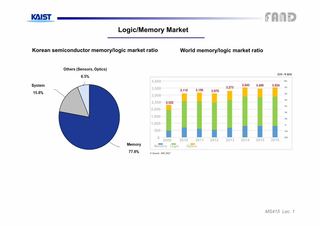
Logic/Memory Market
World memory/logic market ratioKorean semiconductor memory/logic market ratio
2009 2010 2011 2012 2013 2014 2015 2016
500
0
1,000
1,500
2,000
2,500
3,000
3,500
4,000
Memory Logic Optics
MS415 Lec. 116
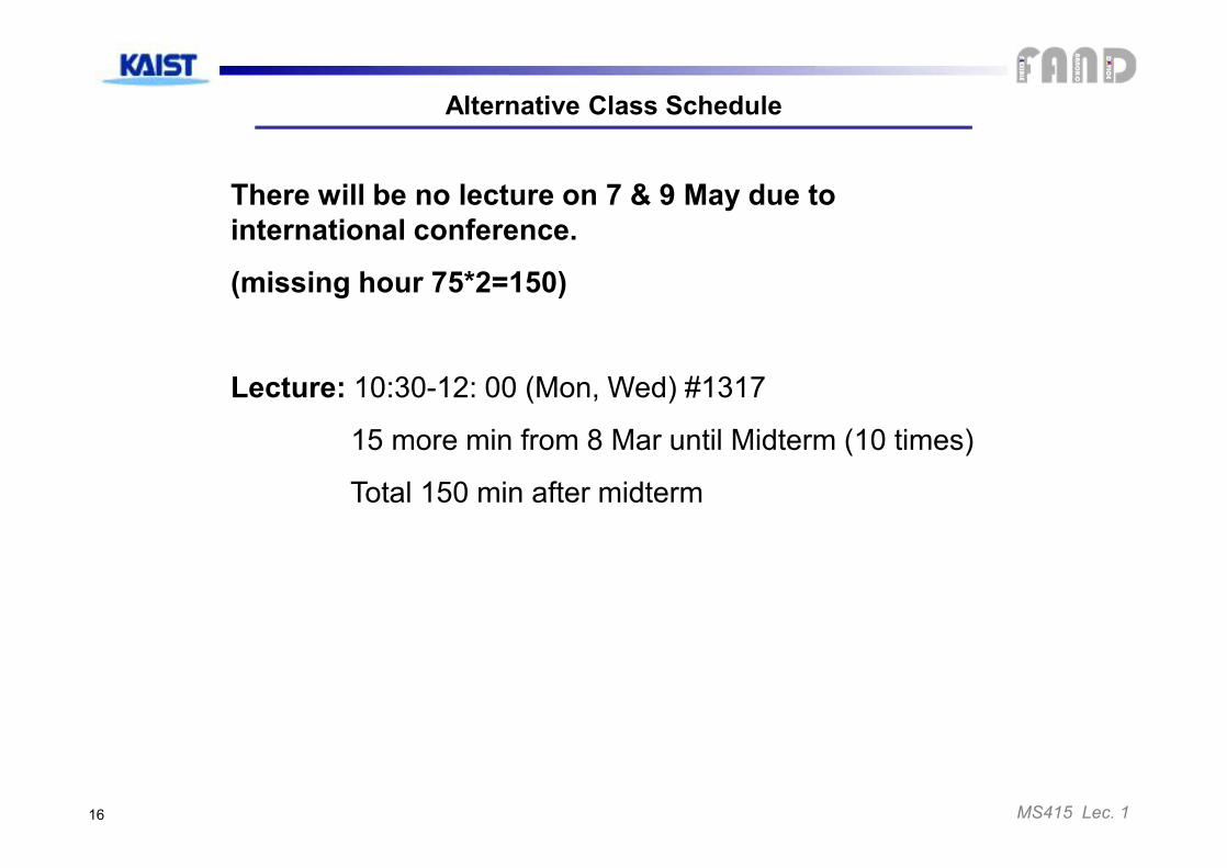
There will be no lecture on 7 & 9 May due to international conference.
(missing hour 75*2=150)
Lecture: 10:30-12: 00 (Mon, Wed) #1317
15 more min from 8 Mar until Midterm (10 times)
Total 150 min after midterm
Alternative Class Schedule