Embed Size (px)
Citation preview
DS-IXD_609-R01 www.clare.com 1
RoHS2002/95/EC e3Pb
Features• 9A Peak Source/Sink Drive Current• Wide Operating Voltage Range: 4.5V to 35V• -40°C to +125°C Extended Operating Temperature
Range• Logic Input Withstands Negative Swing of up to 5V• Matched Rise and Fall Times• Low Propagation Delay Time• Low, 10μA Supply Current• Low Output Impedance
Applications• Efficient Power MOSFET and IGBT Switching• Switch Mode Power Supplies• Motor Controls• DC to DC Converters• Class-D Switching Amplifiers• Pulse Transformer Driver
DescriptionThe IXDD609/IXDI609/IXDN609 high-speed gate drivers are especially well suited for driving the latest IXYS MOSFETs and IGBTs. The IXD_609 high-current output can source and sink 9A of peak current while producing voltage rise and fall times of less than 25ns. The input is CMOS compatible, and is virtually immune to latch up. Proprietary circuitry eliminates cross-conduction and current “shoot-through.” Low propagation delay and fast, matched rise and fall times make the IXD_609 family ideal for high-frequency and high-power applications.
The IXDD609 is configured as a non-inverting driver with an enable, the IXDN609 is configured as a non-inverting driver, and the IXDI609 is configured as an inverting driver.
The IXD_609 family is available in a standard 8-pin DIP (PI); an 8-pin SOIC (SIA); an 8-pin Power SOIC with an exposed metal back (SI); an 8-pin DFN (D2); a 5-pin TO-263 (YI); and a 5-pin TO-220 (CI).
Ordering Information
Part Number Logic Configuration Package Type Packing
Method Quantity
IXDD609D2TR 8-Pin DFN Tape & Reel 2000IXDD609SI 8-Pin Power SOIC with Exposed Metal Back Tube 100IXDD609SITR 8-Pin Power SOIC with Exposed Metal Back Tape & Reel 2000IXDD609SIA 8-Pin SOIC Tube 100IXDD609SIATR 8-Pin SOIC Tape & Reel 2000IXDD609PI 8-Pin DIP Tube 50IXDD609CI 5-Pin TO-220 Tube 50IXDD609YI 5-Pin TO-263 Tube 50IXDI609SI 8-Pin Power SOIC with Exposed Metal Back Tube 100IXDI609SITR 8-Pin Power SOIC with Exposed Metal Back Tape & Reel 2000IXDI609SIA 8-Pin SOIC Tube 100IXDI609SIATR 8-Pin SOIC Tape & Reel 2000IXDI609PI 8-Pin DIP Tube 50IXDI609CI 5-Pin TO-220 Tube 50IXDI609YI 5-Pin TO-263 Tube 50IXDN609SI 8-Pin Power SOIC with Exposed Metal Back Tube 100IXDN609SITR 8-Pin Power SOIC with Exposed Metal Back Tape & Reel 2000IXDN609SIA 8-Pin SOIC Tube 100IXDN609SIATR 8-Pin SOIC Tape & Reel 2000IXDN609PI 8-Pin DIP Tube 50IXDN609CI 5-Pin TO-220 Tube 50IXDN609YI 5-Pin TO-263 Tube 50
IN
EN
OUT
IN OUT
IN OUT
IXD_6099-Ampere Low-Side
Ultrafast MOSFET Drivers
IXD_609
R01 www.clare.com 2
1. Specifications . . . . . . . . . . . . . . . . . . . . . . . . . . . . . . . . . . . . . . . . . . . . . . . . . . . . . . . . . . . . . . . . . . . . . . . . . . . . . . . . . . . . . . . . . . . . . . 31.1 Pin Configurations . . . . . . . . . . . . . . . . . . . . . . . . . . . . . . . . . . . . . . . . . . . . . . . . . . . . . . . . . . . . . . . . . . . . . . . . . . . . . . . . . . . . . . . 31.2 Pin Definitions . . . . . . . . . . . . . . . . . . . . . . . . . . . . . . . . . . . . . . . . . . . . . . . . . . . . . . . . . . . . . . . . . . . . . . . . . . . . . . . . . . . . . . . . . . 31.3 Absolute Maximum Ratings . . . . . . . . . . . . . . . . . . . . . . . . . . . . . . . . . . . . . . . . . . . . . . . . . . . . . . . . . . . . . . . . . . . . . . . . . . . . . . . . 31.4 Recommended Operating Conditions . . . . . . . . . . . . . . . . . . . . . . . . . . . . . . . . . . . . . . . . . . . . . . . . . . . . . . . . . . . . . . . . . . . . . . . . 31.5 Electrical Characteristics: TA = 25°C . . . . . . . . . . . . . . . . . . . . . . . . . . . . . . . . . . . . . . . . . . . . . . . . . . . . . . . . . . . . . . . . . . . . . . . . . 41.6 Electrical Characteristics: TA = - 40°C to +125°C . . . . . . . . . . . . . . . . . . . . . . . . . . . . . . . . . . . . . . . . . . . . . . . . . . . . . . . . . . . . . . . 41.7 Thermal Characteristics . . . . . . . . . . . . . . . . . . . . . . . . . . . . . . . . . . . . . . . . . . . . . . . . . . . . . . . . . . . . . . . . . . . . . . . . . . . . . . . . . . . 5
2. IXD_609 Performance . . . . . . . . . . . . . . . . . . . . . . . . . . . . . . . . . . . . . . . . . . . . . . . . . . . . . . . . . . . . . . . . . . . . . . . . . . . . . . . . . . . . . . . . 52.1 Timing Diagrams . . . . . . . . . . . . . . . . . . . . . . . . . . . . . . . . . . . . . . . . . . . . . . . . . . . . . . . . . . . . . . . . . . . . . . . . . . . . . . . . . . . . . . . . 52.2 Characteristics Test Diagram. . . . . . . . . . . . . . . . . . . . . . . . . . . . . . . . . . . . . . . . . . . . . . . . . . . . . . . . . . . . . . . . . . . . . . . . . . . . . . . 5
3. Block Diagrams & Truth Tables . . . . . . . . . . . . . . . . . . . . . . . . . . . . . . . . . . . . . . . . . . . . . . . . . . . . . . . . . . . . . . . . . . . . . . . . . . . . . . . . 63.1 IXDD609 . . . . . . . . . . . . . . . . . . . . . . . . . . . . . . . . . . . . . . . . . . . . . . . . . . . . . . . . . . . . . . . . . . . . . . . . . . . . . . . . . . . . . . . . . . . . . . 63.2 IXDI609 . . . . . . . . . . . . . . . . . . . . . . . . . . . . . . . . . . . . . . . . . . . . . . . . . . . . . . . . . . . . . . . . . . . . . . . . . . . . . . . . . . . . . . . . . . . . . . . 63.3 IXDN609 . . . . . . . . . . . . . . . . . . . . . . . . . . . . . . . . . . . . . . . . . . . . . . . . . . . . . . . . . . . . . . . . . . . . . . . . . . . . . . . . . . . . . . . . . . . . . . 6
4. Typical Performance Characteristics . . . . . . . . . . . . . . . . . . . . . . . . . . . . . . . . . . . . . . . . . . . . . . . . . . . . . . . . . . . . . . . . . . . . . . . . . . . 7
5. Manufacturing Information . . . . . . . . . . . . . . . . . . . . . . . . . . . . . . . . . . . . . . . . . . . . . . . . . . . . . . . . . . . . . . . . . . . . . . . . . . . . . . . . . . . 105.1 Moisture Sensitivity . . . . . . . . . . . . . . . . . . . . . . . . . . . . . . . . . . . . . . . . . . . . . . . . . . . . . . . . . . . . . . . . . . . . . . . . . . . . . . . . . . . . . 105.2 ESD Sensitivity . . . . . . . . . . . . . . . . . . . . . . . . . . . . . . . . . . . . . . . . . . . . . . . . . . . . . . . . . . . . . . . . . . . . . . . . . . . . . . . . . . . . . . . . 105.3 Reflow Profile. . . . . . . . . . . . . . . . . . . . . . . . . . . . . . . . . . . . . . . . . . . . . . . . . . . . . . . . . . . . . . . . . . . . . . . . . . . . . . . . . . . . . . . . . . 105.4 Mechanical Dimensions. . . . . . . . . . . . . . . . . . . . . . . . . . . . . . . . . . . . . . . . . . . . . . . . . . . . . . . . . . . . . . . . . . . . . . . . . . . . . . . . . . 11
IXD_609
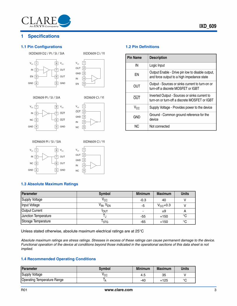
1 Specifications
1.1 Pin Configurations 1.2 Pin Definitions
1.3 Absolute Maximum Ratings
Unless stated otherwise, absolute maximum electrical ratings are at 25°C
Absolute maximum ratings are stress ratings. Stresses in excess of these ratings can cause permanent damage to the device. Functional operation of the device at conditions beyond those indicated in the operational sections of this data sheet is not implied.
1.4 Recommended Operating Conditions
1
4
3
2
8
5
6
7
VCC
IN
EN
GND
VCC
OUT
OUT
GND
1
4
3
2
5
VCC
OUT
GND
IN
EN
1
4
3
2
8
5
6
7
VCC
IN
NC
GND
VCC
OUT
OUT
GND
1
4
3
2
5
VCC
OUT
GND
IN
NC
1
4
3
2
8
5
6
7
VCC
IN
NC
GND
VCC
OUT
OUT
GND
1
4
3
2
5
VCC
OUT
GND
IN
NC
IXDD609 D2 / PI / SI / SIA
IXDI609 PI / SI / SIA
IXDN609 PI / SI / SIA
IXDD609 CI / YI
IXDI609 CI / YI
IXDN609 CI / YI
Pin Name Description
IN Logic Input
ENOutput Enable - Drive pin low to disable output, and force output to a high impedance state
OUTOutput - Sources or sinks current to turn-on or turn-off a discrete MOSFET or IGBT
OUTInverted Output - Sources or sinks current to turn-on or turn-off a discrete MOSFET or IGBT
VCC Supply Voltage - Provides power to the device
GNDGround - Common ground reference for the device
NC Not connected
Parameter Symbol Minimum Maximum Units
Supply Voltage VCC -0.3 40 V
Input Voltage VIN, VEN -5 VCC+0.3 VOutput Current IOUT - ±9 AJunction Temperature TJ -55 +150 °C
Storage Temperature TSTG -65 +150 °C
Parameter Symbol Minimum Maximum Units
Supply Voltage VCC 4.5 35 VOperating Temperature Range TA -40 +125 °C
R01 www.clare.com 3
IXD_609
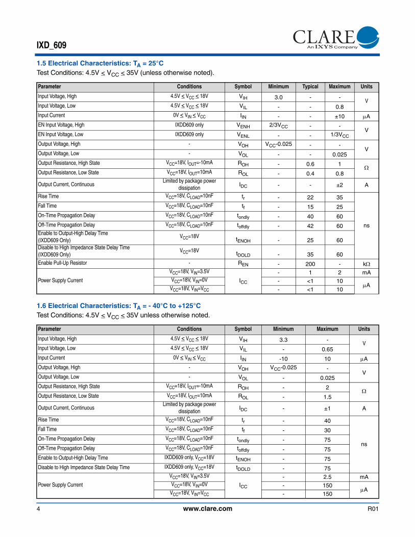
1.5 Electrical Characteristics: TA = 25°CTest Conditions: 4.5V < VCC < 35V (unless otherwise noted).
1.6 Electrical Characteristics: TA = - 40°C to +125°CTest Conditions: 4.5V < VCC < 35V unless otherwise noted.
Parameter Conditions Symbol Minimum Typical Maximum Units
Input Voltage, High 4.5V < VCC < 18V VIH 3.0 - -V
Input Voltage, Low 4.5V < VCC < 18V VIL - - 0.8
Input Current 0V < VIN < VCC IIN - - ±10 μA
EN Input Voltage, High IXDD609 only VENH 2/3VCC - -V
EN Input Voltage, Low IXDD609 only VENL - - 1/3VCC
Output Voltage, High - VOH VCC-0.025 - -V
Output Voltage, Low - VOL - - 0.025
Output Resistance, High State VCC=18V, IOUT=-10mA ROH - 0.6 1Ω
Output Resistance, Low State VCC=18V, IOUT=10mA ROL - 0.4 0.8
Output Current, ContinuousLimited by package power
dissipationIDC - - ±2 A
Rise Time VCC=18V, CLOAD=10nF tr - 22 35
ns
Fall Time VCC=18V, CLOAD=10nF tf - 15 25
On-Time Propagation Delay VCC=18V, CLOAD=10nF tondly - 40 60
Off-Time Propagation Delay VCC=18V, CLOAD=10nF toffdly - 42 60Enable to Output-High Delay Time(IXDD609 Only)
VCC=18V tENOH - 25 60Disable to High Impedance State Delay Time(IXDD609 Only)
VCC=18V tDOLD - 35 60
Enable Pull-Up Resistor - REN - 200 - kΩ
Power Supply Current
VCC=18V, VIN=3.5V
ICC
- 1 2 mAVCC=18V, VIN=0V - <1 10
μAVCC=18V, VIN=VCC - <1 10
Parameter Conditions Symbol Minimum Maximum Units
Input Voltage, High 4.5V < VCC < 18V VIH 3.3 -V
Input Voltage, Low 4.5V < VCC < 18V VIL - 0.65
Input Current 0V < VIN < VCC IIN -10 10 μA
Output Voltage, High - VOH VCC-0.025 -V
Output Voltage, Low - VOL - 0.025
Output Resistance, High State VCC=18V, IOUT=-10mA ROH - 2Ω
Output Resistance, Low State VCC=18V, IOUT=10mA ROL - 1.5
Output Current, ContinuousLimited by package power
dissipationIDC - ±1 A
Rise Time VCC=18V, CLOAD=10nF tr - 40
ns
Fall Time VCC=18V, CLOAD=10nF tf - 30
On-Time Propagation Delay VCC=18V, CLOAD=10nF tondly - 75
Off-Time Propagation Delay VCC=18V, CLOAD=10nF toffdly - 75
Enable to Output-High Delay Time IXDD609 only, VCC=18V tENOH - 75
Disable to High Impedance State Delay Time IXDD609 only, VCC=18V tDOLD - 75
Power Supply Current
VCC=18V, VIN=3.5V
ICC
- 2.5 mAVCC=18V, VIN=0V - 150
μAVCC=18V, VIN=VCC - 150
4 www.clare.com R01
IXD_609
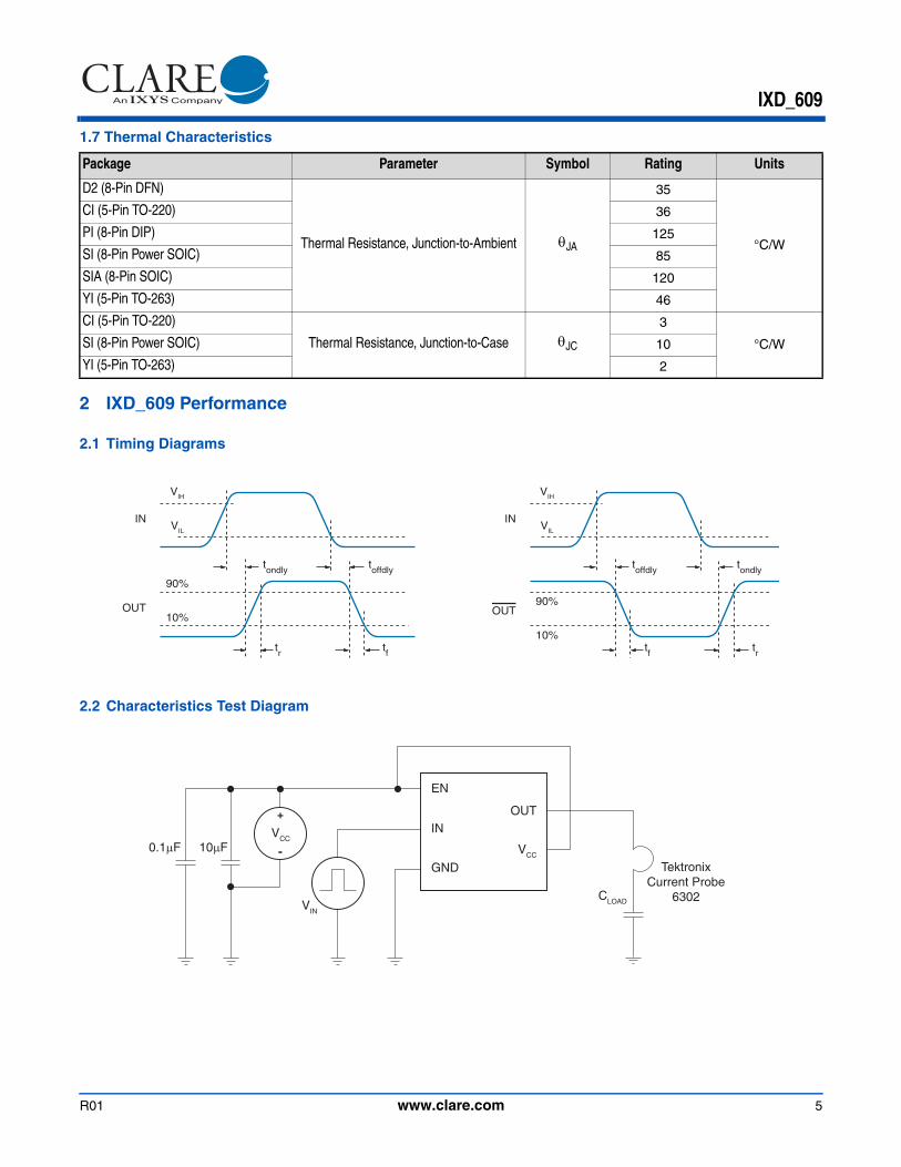
1.7 Thermal Characteristics
2 IXD_609 Performance
2.1 Timing Diagrams
2.2 Characteristics Test Diagram
Package Parameter Symbol Rating Units
D2 (8-Pin DFN)
Thermal Resistance, Junction-to-Ambient θJA
35
°C/W
CI (5-Pin TO-220) 36
PI (8-Pin DIP) 125
SI (8-Pin Power SOIC) 85
SIA (8-Pin SOIC) 120
YI (5-Pin TO-263) 46
CI (5-Pin TO-220)
Thermal Resistance, Junction-to-Case θJC
3
°C/WSI (8-Pin Power SOIC) 10
YI (5-Pin TO-263) 2
10%
90%
tondly toffdly
tr tf
VIH
VIL
IN
OUT
10%
90%
tondlytoffdly
tf tr
VIH
VIL
IN
OUT
EN
INOUT
GND
VCC
VCC
+
-
VIN
0.1μF 10μF
TektronixCurrent Probe
6302CLOAD
R01 www.clare.com 5
IXD_609
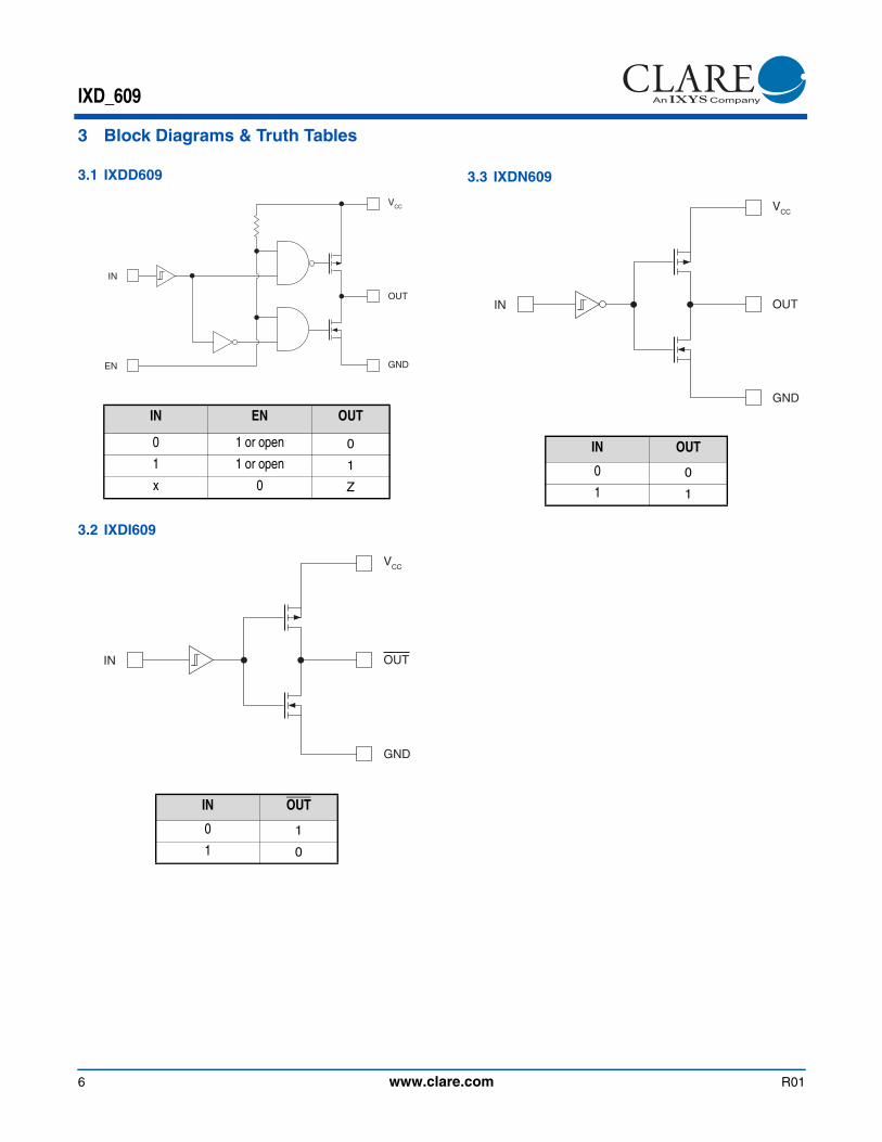
3 Block Diagrams & Truth Tables
3.1 IXDD609
3.2 IXDI609
3.3 IXDN609
IN EN OUT
0 1 or open 0
1 1 or open 1
x 0 Z
IN OUT
0 1
1 0
GND
IN
EN
VCC
OUT
IN
VCC
GND
OUT
IN OUT
0 0
1 1
IN
VCC
GND
OUT
6 www.clare.com R01
IXD_609
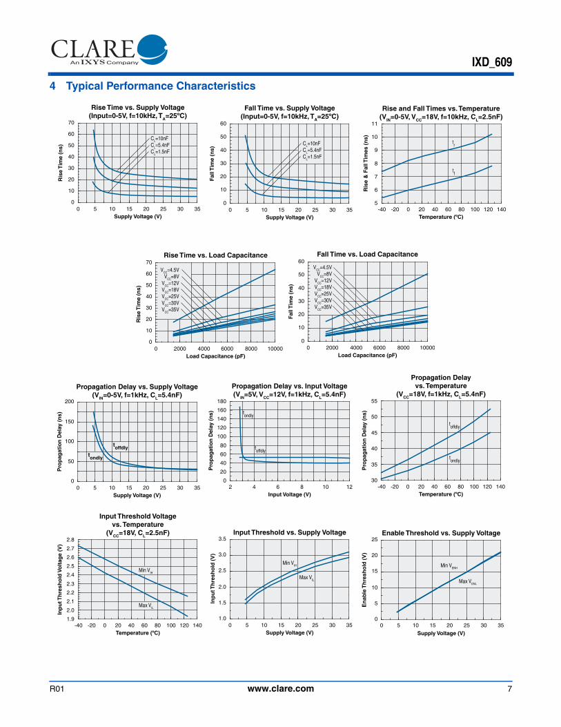
4 Typical Performance Characteristics
Supply Voltage (V)0 5 10 15 20 25 30 35
Ris
e T
ime
(ns)
0
10
20
30
40
50
60
70
Rise Time vs. Supply Voltage(Input=0-5V, f=10kHz, TA=25ºC)
CL=10nFCL=5.4nFCL=1.5nF
Supply Voltage (V)0 5 10 15 20 25 30 35
Fall
Tim
e (n
s)
0
10
20
30
40
50
60
Fall Time vs. Supply Voltage(Input=0-5V, f=10kHz, TA=25ºC)
CL=10nFCL=5.4nFCL=1.5nF
Temperature (ºC)-40 -20 0 20 40 60 80 100 120 140
Ris
e &
Fal
l Tim
es (
ns)
5
6
7
8
9
10
11
Rise and Fall Times vs. Temperature(VIN=0-5V, VCC=18V, f=10kHz, CL=2.5nF)
tr
tf
Load Capacitance (pF)0 2000 4000 6000 8000 10000
Ris
e T
ime
(ns)
0
10
20
30
40
50
60
70Rise Time vs. Load Capacitance
VCC=4.5VVCC=8V
VCC=12VVCC=18VVCC=25VVCC=30VVCC=35V
Load Capacitance (pF)0 2000 4000 6000 8000 10000
Fall
Tim
e (n
s)
0
10
20
30
40
50
60Fall Time vs. Load Capacitance
VCC=4.5VVCC=8V
VCC=12VVCC=18VVCC=25VVCC=30VVCC=35V
Supply Voltage (V)0 5 10 15 20 25 30 35
Pro
pag
atio
n D
elay
(n
s)
0
50
100
150
200
Propagation Delay vs. Supply Voltage(VIN=0-5V, f=1kHz, CL=5.4nF)
toffdly
tondly
Input Voltage (V)2 4 6 8 10 12
Pro
pag
atio
n D
elay
(n
s)
0
20
40
60
80
100
120
140
160
180
Propagation Delay vs. Input Voltage(VIN=5V, VCC=12V, f=1kHz, CL=5.4nF)
tondly
toffdly
Temperature (ºC)-40 -20 0 20 40 60 80 100 120 140
Pro
pag
atio
n D
elay
(n
s)
30
35
40
45
50
55
Propagation Delayvs. Temperature
(VCC=18V, f=1kHz, CL=5.4nF)
tondly
toffdly
Temperature (ºC)-40 -20 0 20 40 60 80 100 120 140
Inp
ut T
hre
sho
ld V
olt
age
(V)
1.9
2.0
2.1
2.2
2.3
2.4
2.5
2.6
2.7
2.8
Input Threshold Voltagevs. Temperature
(VCC=18V, CL=2.5nF)
Min VIH
Max VIL
Supply Voltage (V)0 5 10 15 20 25 30 35
Inp
ut T
hre
sho
ld (
V)
1.0
1.5
2.0
2.5
3.0
3.5Input Threshold vs. Supply Voltage
Min VIH
Max VIL
Supply Voltage (V)0 5 10 15 20 25 30 35
En
able
Th
resh
old
(V
)
0
5
10
15
20
25Enable Threshold vs. Supply Voltage
Min VENH
Max VENL
R01 www.clare.com 7
IXD_609
Load Capacitance (pF)1000 10000
Su
pp
ly C
urr
ent
(mA
)
0
100
200
300
400
500
Supply Current vs. Load Capacitance(VCC=18V)
f=2MHzf=1MHz
f=500kHzf=100kHzf=50kHzf=10kHzf=1kHz
Load Capacitance (pF)1000 10000
Su
pp
ly C
urr
ent
(mA
)
0
50
100
150
200
250
300
Supply Current vs. Load Capacitance(VCC=12V)
f=2MHzf=1MHz
f=500kHzf=100kHzf=50kHzf=10kHzf=1kHz
Load Capacitance (pF)1000 10000
Su
pp
ly C
urr
ent
(mA
)
0
50
100
150
200
Supply Current vs. Load Capacitance(VCC=8V)
f=2MHzf=1MHz
f=500kHzf=100kHzf=50kHzf=10kHzf=1kHz
Frequency (kHz)1 10 100 1000 10000
Su
pp
ly C
urr
ent
(mA
)
0.1
1
10
100
1000
Supply Current vs. Frequency(VCC=18V)
CL=10nFCL=5.4nFCL=1.5nF
Frequency (kHz)1 10 100 1000 10000
Su
pp
ly C
urr
ent
(mA
)
0.1
1
10
100
1000
Supply Current vs. Frequency(VCC=12V)
CL=10nFCL=5.4nFCL=1.5nF
Frequency (kHz)1 10 100 1000 10000
Su
pp
ly C
urr
ent
(mA
)
0.01
0.1
1
10
100
1000
Supply Current vs. Frequency(VCC=8V)
CL=10nFCL=5.4nFCL=1.5nF
Temperature (ºC)-40 -20 0 20 40 60 80 100 120 140
Su
pp
ly C
urr
ent
(mA
)
0.0
0.2
0.4
0.6
0.8
1.0
1.2
1.4
Quiescent Supply Currentvs. Temperature
VIN=3.5VVIN=5VVIN=10V
VIN=0V & 18V
Temperature (ºC)-40 -20 0 20 40 60 80 100 120 140
Su
pp
ly C
urr
ent
(mA
)
0.35
0.40
0.45
0.50
0.55
0.60
0.65
Dynamic Supply Currentvs. Temperature
(VIN=5V, VCC=18V, f=1kHz, CL=1.5nF)
Supply Voltage (V)0 5 10 15 20 25 30 35
Ou
tpu
t S
ou
rce
Cu
rren
t (A
)
0
-5
-10
-15
-20
-25
-30
Output Source Currentvs. Supply Voltage(f=422Hz, CL=66nF)
Supply Voltage (V)0 5 10 15 20 25 30 35
Ou
tpu
t S
ink
Cu
rren
t (A
)
0
5
10
15
20
25
30
Output Sink Currentvs. Supply Voltage(f=422Hz, CL=66nF)
8 www.clare.com R01
IXD_609
Temperature (ºC)-40 -20 0 20 40 60 80 100 120 140
Ou
tpu
t S
ou
rce
Cu
rren
t (A
)
-9.0
-9.5
-10.0
-10.5
-11.0
-11.5
-12.0
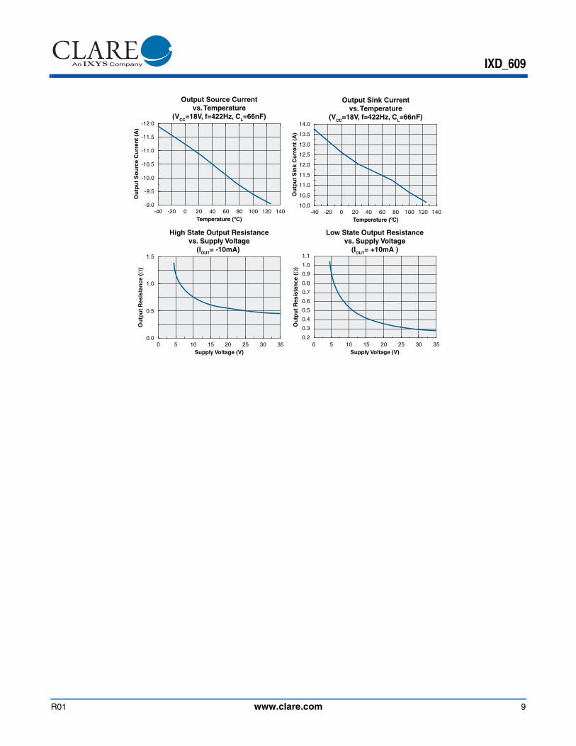
Output Source Currentvs. Temperature
(VCC=18V, f=422Hz, CL=66nF)
Temperature (ºC)-40 -20 0 20 40 60 80 100 120 140
Ou
tpu
t S
ink
Cu
rren
t (A
)
10.0
10.5
11.0
11.5
12.0
12.5
13.0
13.5
14.0
Output Sink Currentvs. Temperature
(VCC=18V, f=422Hz, CL=66nF)
Supply Voltage (V)0 5 10 15 20 25 30 35
Ou
tpu
t R
esis
tan
ce (Ω
)
0.0
0.5
1.0
1.5
High State Output Resistancevs. Supply Voltage
(IOUT= -10mA)
Supply Voltage (V)0 5 10 15 20 25 30 35
Ou
tpu
t R
esis
tan
ce (Ω
)
0.2
0.3
0.4
0.5
0.6
0.7
0.8
0.9
1.0
1.1
Low State Output Resistancevs. Supply Voltage
(IOUT= +10mA )
R01 www.clare.com 9
IXD_609
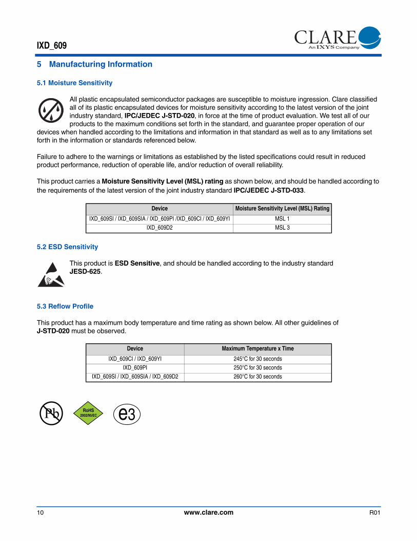
5 Manufacturing Information
5.1 Moisture Sensitivity
All plastic encapsulated semiconductor packages are susceptible to moisture ingression. Clare classified all of its plastic encapsulated devices for moisture sensitivity according to the latest version of the joint industry standard, IPC/JEDEC J-STD-020, in force at the time of product evaluation. We test all of our products to the maximum conditions set forth in the standard, and guarantee proper operation of our
devices when handled according to the limitations and information in that standard as well as to any limitations set forth in the information or standards referenced below.
Failure to adhere to the warnings or limitations as established by the listed specifications could result in reduced product performance, reduction of operable life, and/or reduction of overall reliability.
This product carries a Moisture Sensitivity Level (MSL) rating as shown below, and should be handled according to the requirements of the latest version of the joint industry standard IPC/JEDEC J-STD-033.
5.2 ESD Sensitivity
This product is ESD Sensitive, and should be handled according to the industry standard JESD-625.
5.3 Reflow Profile
This product has a maximum body temperature and time rating as shown below. All other guidelines of J-STD-020 must be observed.
Device Moisture Sensitivity Level (MSL) Rating
IXD_609SI / IXD_609SIA / IXD_609PI /IXD_609CI / IXD_609YI MSL 1
IXD_609D2 MSL 3
Device Maximum Temperature x Time
IXD_609CI / IXD_609YI 245°C for 30 secondsIXD_609PI 250°C for 30 seconds
IXD_609SI / IXD_609SIA / IXD_609D2 260°C for 30 seconds
RoHS2002/95/EC e3Pb
10 www.clare.com R01
IXD_609
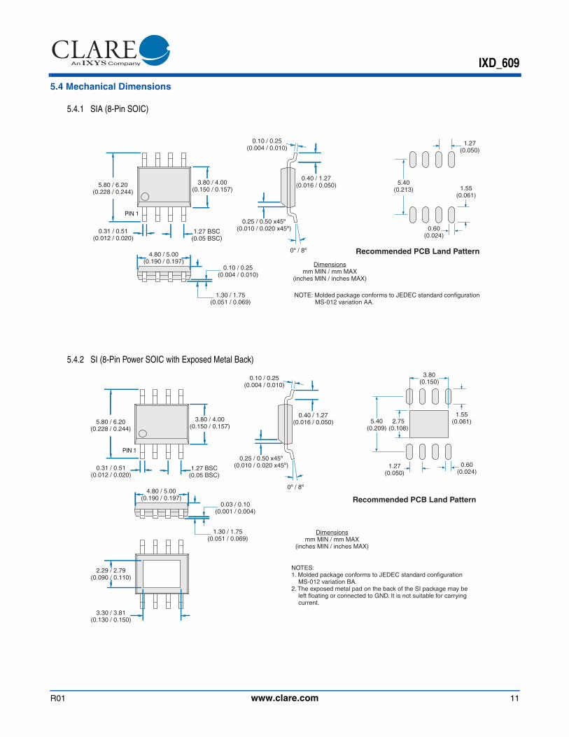
5.4 Mechanical Dimensions
5.4.1 SIA (8-Pin SOIC)
5.4.2 SI (8-Pin Power SOIC with Exposed Metal Back)
Recommended PCB Land Pattern
Dimensionsmm MIN / mm MAX
(inches MIN / inches MAX)
1.30 / 1.75(0.051 / 0.069)
0.10 / 0.25(0.004 / 0.010)
4.80 / 5.00(0.190 / 0.197)
PIN 1
0.31 / 0.51(0.012 / 0.020)
5.80 / 6.20(0.228 / 0.244)
3.80 / 4.00(0.150 / 0.157)
1.27 BSC(0.05 BSC)
0.40 / 1.27(0.016 / 0.050)
0.10 / 0.25(0.004 / 0.010)
0.25 / 0.50 x45º(0.010 / 0.020 x45º)
0º / 8º
1.27(0.050)
5.40(0.213) 1.55
(0.061)
0.60(0.024)
NOTE: Molded package conforms to JEDEC standard configuration MS-012 variation AA.
Recommended PCB Land Pattern
Dimensionsmm MIN / mm MAX
(inches MIN / inches MAX)
NOTES: 1. Molded package conforms to JEDEC standard configuration MS-012 variation BA.2. The exposed metal pad on the back of the SI package may be left floating or connected to GND. It is not suitable for carrying current.
1.30 / 1.75(0.051 / 0.069)
0.03 / 0.10(0.001 / 0.004)
4.80 / 5.00(0.190 / 0.197)
PIN 1
0.31 / 0.51(0.012 / 0.020)
5.80 / 6.20(0.228 / 0.244)
3.80 / 4.00(0.150 / 0.157)
1.27 BSC(0.05 BSC)
0.40 / 1.27(0.016 / 0.050)
0.10 / 0.25(0.004 / 0.010)
0.25 / 0.50 x45º(0.010 / 0.020 x45º)
0º / 8º
2.29 / 2.79(0.090 / 0.110)
3.30 / 3.81(0.130 / 0.150)
1.27(0.050)
5.40(0.209)
1.55(0.061)
0.60(0.024)
2.75(0.108)
3.80(0.150)
R01 www.clare.com 11
IXD_609
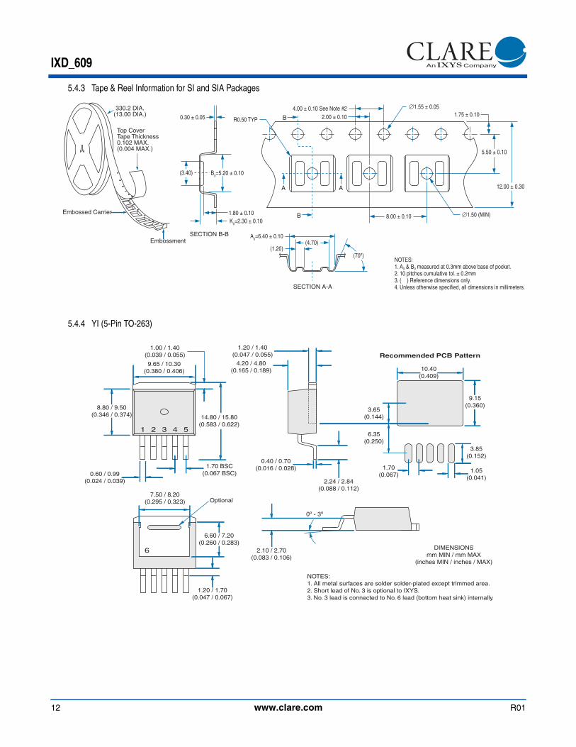
5.4.3 Tape & Reel Information for SI and SIA Packages
5.4.4 YI (5-Pin TO-263)
NOTES:1. A0 & B0 measured at 0.3mm above base of pocket.2. 10 pitches cumulative tol. ± 0.2mm3. ( ) Reference dimensions only.4. Unless otherwise specified, all dimensions in millimeters.
K0=2.30 ± 0.10
B0=5.20 ± 0.10
R0.50 TYP
8.00 ± 0.10
2.00 ± 0.104.00 ± 0.10 See Note #2
12.00 ± 0.30
5.50 ± 0.10
1.75 ± 0.10
∅1.50 (MIN)
∅1.55 ± 0.05
1.80 ± 0.10
(3.40)
0.30 ± 0.05
(70º)
A0=6.40 ± 0.10(4.70)
(1.20)
A A
B
B
SECTION A-A
SECTION B-BEmbossment
Embossed Carrier
Top CoverTape Thickness0.102 MAX.(0.004 MAX.)
330.2 DIA.(13.00 DIA.)
DIMENSIONSmm MIN / mm MAX
(inches MIN / inches / MAX)
NOTES:1. All metal surfaces are solder solder-plated except trimmed area.2. Short lead of No. 3 is optional to IXYS.3. No. 3 lead is connected to No. 6 lead (bottom heat sink) internally.
8.80 / 9.50(0.346 / 0.374) 14.80 / 15.80
(0.583 / 0.622)
9.65 / 10.30(0.380 / 0.406)
1.70 BSC(0.067 BSC)
1 2 3 4 5
0.60 / 0.99(0.024 / 0.039)
1.00 / 1.40(0.039 / 0.055)
4.20 / 4.80(0.165 / 0.189)
1.20 / 1.40(0.047 / 0.055)
0.40 / 0.70(0.016 / 0.028)
2.24 / 2.84(0.088 / 0.112)
2.10 / 2.70(0.083 / 0.106)
0º - 3º
6.60 / 7.20(0.260 / 0.283)
7.50 / 8.20(0.295 / 0.323)
1.20 / 1.70(0.047 / 0.067)
6
Optional
3.85(0.152)
3.65(0.144)
6.35(0.250)
1.05(0.041)
1.70(0.067)
10.40(0.409)
9.15(0.360)
Recommended PCB Pattern
12 www.clare.com R01

IXD_609
5.4.5 PI (8-Pin DIP)
5.4.6 CI (5-Pin TO-220)
Dimensionsmm MIN / mm MAX
(inches MIN / inches MAX)
NOTE: Molded package conforms to JEDEC standard configuration MS-001 variation BA.
PC Board Pattern7.62 / 10.92
(0.300 / 0.430)
7.62 BSC(0.300 BSC)
0.20 / 0.38(0.008 / 0.015)
7.37 / 8.26(0.290 / 0.325)
0.38 / 0.58(0.015 / 0.023)
1.14 / 1.65(0.045 / 0.065)
0.38 / 1.02(0.015 / 0.040)
3.05 / 3.81(0.120 / 0.150) 3.43 / 4.70
(0.135 / 0.185)
3.18 / 3.81(0.125 / 0.150)
8-0.900 DIA.(8-0.035 DIA.)
7.50(0.295)
2.540(0.100)
9.02 / 10.16(0.355 / 0.400)
6.10 / 6.86(0.240 / 0.270)
2.540 BSC(0.100 BSC)
1.40(0.055)
NOTES: 1. This drawing will meet all dimensions requirement of JEDEC outlines TS-001AA and 5-lead version TO-220AB.2. Mounting hole diameter: 3.53 / 3.96 (0.139 / 0.156)3. The metal tab is connected to pin 3 (GND).
25.27 / 26.54(0.995 / 1.045)
11.94 / 12.95(0.470 / 0.510)
14.73 / 15.75(0.580 / 0.620)
9.91 / 10.54(0.390 / 0.415)
1.70 BSC(0.067 BSC)0.64 / 1.02
(0.025 / 0.040)
8.64 / 9.40(0.340 / 0.370)
4.32 / 4.83(0.170 / 0.190)
1.14 / 1.40(0.045 / 0.055)
0.38 / 0.64(0.015 / 0.025)
2.29 / 2.92(0.090 / 0.115)
DIMENSIONSmm MIN / mm MAX
(inches MIN / inches / MAX)
Finished Hole Diameter = 1.45mm (0.057 in.)Recommended Hole Pattern
1.70mm (0.067 in.)
R01 www.clare.com 13
IXD_609
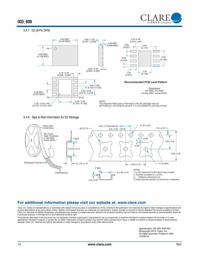
5.4.7 D2 (8-Pin DFN)
5.4.8 Tape & Reel Information for D2 Package
Dimensionsmm MIN / mm MAX
(inches MIN / inches MAX)
5.00 BSC(0.197 BSC)
4.00 BSC(0.158 BSC)
0.80 / 1.00(0.031 / 0.039)
0.00 / 0.05(0.000 / 0.002)
0.95 BSC(0.037 BSC)
0.76 / 0.81(0.030 / 0.032)
0.30 / 0.45(0.012 / 0.018)
3.04 / 3.09(0.120 / 0.122)
2.54 / 2.59(0.100 / 0.102)0.35 / 0.45 x 45º
(0.014 / 0.018 x 45º)
Pin 1
Pin 1 Pin 8
0.20 REF(0.008 REF)
Recommended PCB Land Pattern
4.50(0.177)
0.45(0.018)
1.20(0.047)
3.05(0.120)
2.55(0.100)
0.95(0.037)
0.35 x 45º(0.014 x 45º)
NOTE:The exposed metal pad on the back of the D2 package may beleft floating or connected to ground. It is not suitable for carrying current.
K0=1.90 ± 0.10
B0=5.40 ± 0.10
5º MAX
A0=4.25 ± 0.10
5º MAX
0.30 ± 0.05
(0.05)
(0.05)
R0.75 TYP
8.00 ± 0.10
2.00 ± 0.054.00 ± 0.10 See Note #2
12.00 ± 0.30
5.50 ± 0.05
1.75 ± 0.10
∅1.50 (MIN)
∅1.55 ± 0.05
NOTES:1. A0 & B0 measured at 0.3mm above base of pocket.2. 10 pitches cumulative tol. ± 0.2mm3. ( ) Reference dimensions only.4. Unless otherwise specified, all dimensions in millimeters.
Embossment
Embossed Carrier
Top CoverTape Thickness0.102 MAX.(0.004 MAX.)
330.2 DIA.(13.00 DIA.)
For additional information please visit our website at: www.clare.comClare, Inc. makes no representations or warranties with respect to the accuracy or completeness of the contents of this publication and reserves the right to make changes to specifications and product descriptions at any time without notice. Neither circuit patent licenses nor indemnity are expressed or implied. Except as set forth in Clare’s Standard Terms and Conditions of Sale, Clare, Inc. assumes no liability whatsoever, and disclaims any express or implied warranty, relating to its products including, but not limited to, the implied warranty of merchantability, fitness for a particular purpose, or infringement of any intellectual property right.
The products described in this document are not designed, intended, authorized or warranted for use as components in systems intended for surgical implant into the body, or in other applications intended to support or sustain life, or where malfunction of Clare’s product may result in direct physical harm, injury, or death to a person or severe property or environmental damage. Clare, Inc. reserves the right to discontinue or make changes to its products at any time without notice.
Specification: DS-IXD_609-R01©Copyright 2010, Clare, Inc.All rights reserved. Printed in USA.12/3/2010
14 www.clare.com R01


![[IxD] Week 09. The Process of Interaction Design](https://img.pdfslide.tips/doc/110x75/58733bba1a28abf21b8b5947/ixd-week-09-the-process-of-interaction-design.jpg)