Embed Size (px)
Citation preview

ECE1352Term Paper
Low Voltage Phase-Locked Loop
Design Technique
Name: Eric HuStudent Number: 982123400
Date: Nov. 14, 2002

Table of Contents
Abstract …………………………………………………………………………pg. 04
Chapter 1 – Introduction ……………………………………………………….. pg. 04
Chapter 2 – Background ……………………………………………………….. pg. 06
Chapter 3 – Voltage Controlled Oscillator ……………………………………...pg. 08LC Oscillator ……………………………………………………………...pg. 08Ring Oscillator ……………………………………………………………pg. 10Schmitt Positive-Feedback Oscillator……………………………………..pg. 12Current Steering Amplifier Oscillator …………………………………….pg. 14
Chapter 4 – Charge Pump ……………………………………………………… pg. 17Basic Structure ……………………………………………………………pg. 17Voltage Doubler ………………………………………………………….. pg. 18
Conclusion ……………………………………………………………………... pg. 20
References ………………………………………………………………………pg. 21
2
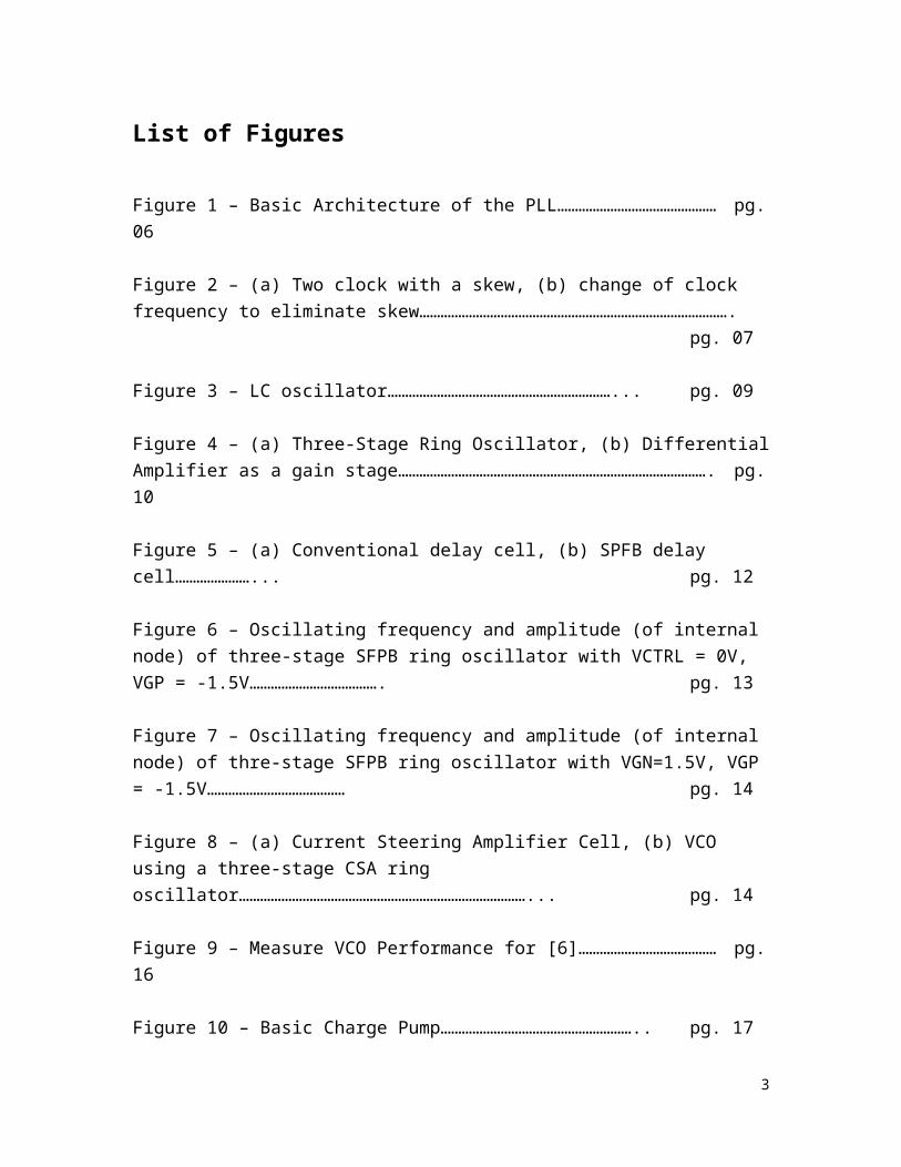
List of Figures
Figure 1 – Basic Architecture of the PLL……………………………………… pg. 06
Figure 2 – (a) Two clock with a skew, (b) change of clock frequency to eliminate skew……………………………………………………………………………. pg. 07
Figure 3 – LC oscillator………………………………………………………... pg. 09
Figure 4 – (a) Three-Stage Ring Oscillator, (b) Differential Amplifier as a gain stage……………………………………………………………………………. pg. 10
Figure 5 – (a) Conventional delay cell, (b) SPFB delay cell…………………... pg. 12
Figure 6 – Oscillating frequency and amplitude (of internal node) of three-stage SFPB ring oscillator with VCTRL = 0V, VGP = -1.5V………………………………. pg. 13
Figure 7 – Oscillating frequency and amplitude (of internal node) of thre-stage SFPB ring oscillator with VGN=1.5V, VGP = -1.5V………………………………… pg. 14
Figure 8 – (a) Current Steering Amplifier Cell, (b) VCO using a three-stage CSA ring oscillator………………………………………………………………………...pg. 14
Figure 9 – Measure VCO Performance for [6]………………………………… pg. 16
Figure 10 – Basic Charge Pump……………………………………………….. pg. 17
Figure 11 – PLL with Voltage Doubler inserted……………………………….. pg. 18
Figure 12 – A PLL frequency tuning characteristics utilizing the voltage doubler…………………………………………………………………………. pg. 19
Abstract
3

Phase-Locked Loop has wide range of application in communication. With the trend
of lower supply voltage to reduce the power dissipation of portable wireless devices, the
overall performance of the analog components of the PLL such as the VCO and the
charge pump are affected. This paper reviews the current development on low voltage
PLL design. Techniques on widening the VCO’s tuning range at low level supply voltage
will be compared and discussed.
Chapter 1 - Introduction
Phase-Locked Loop (PLL) is an essential circuit component in electronics and
communication. It is a mixed-signal circuitry with wide applications in the field such as
clock synthesis and multiplication in the microprocessor or programmable logic systems
[8], and skew reduction and timing recovery circuitry in transceiver units [9].
High-speed low power PLL is of particular interest. There is a fast-trend toward
lowering the supply power voltage. Part of this is due to the low power requirement of the
modern portable wireless communication device. With a single low voltage battery at 1 to
2V, the total power dissipation of a device can significantly affect the overall talk-time,
which is a crucial criterion for portable devices such as pagers or cell phones. By
lowering the supply voltage, the dynamic power dissipation of the digital circuit can be
4
reduced, achieving longer talk-time [10]
However, lowering the supply voltage introduces design challenge to the analog
components of the system. As the power supply voltage continues to scale below 1.8V,
the threshold voltage VT in the MOS device does not scale proportionally because
lowering the threshold voltage leads to excessive leakage currents from the digital
circuits. This reduces the voltage headroom required to vertically stack any significant
number of transistors. To ensure proper biasing, the output voltage swing would be
limited and the commonly used cascode configuration in which multiple transistors are
stacked together may not be implemented. This reduces the tuning range of the variable
controlled oscillator (VCO) inside the PLL and lowers the overall performance of the
PLL.
This paper will review the current development in the low voltage Phase-Locked
Loop Design. Design techniques for the various components of the PLL will be compared
and discussed.
5

Chapter 2 - Background
The basic architecture of the Phase-Locked Loop is shown in Figure 1.
Figure 1 – Basic Architecture of the PLL
The four main components of the PLL are the phase detector, charge pump, loop
filter, and the voltage controlled oscillator. The basic operation of the PLL is as follows.
The phase detector receives input from a reference clock and the local clock produced by
the PLL. The phase difference between the two clocks (due to clock skew or different
clocking frequency) is detected. Depending on the whether the phase leads or lags, an up
or down command is sent to the charge pump, which supplies an analog control voltage
to the VCO to adjust the frequency of oscillation. The loop filter is inserted to reduce
high frequency noise being injected into the VCO causing jitter in the clock frequency.
The adjusted clock frequency is then fed back into the phase detector. Depending on the
application, a divide by N device is often inserted to just after the VCO to produce a
6
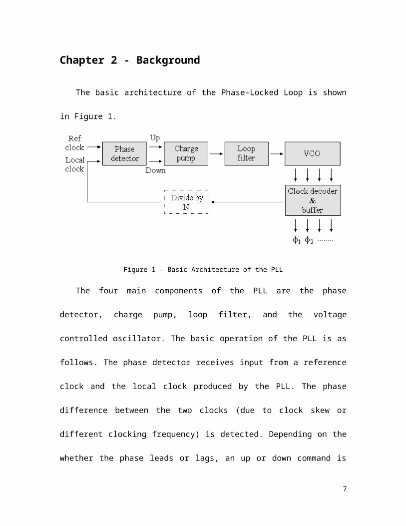
frequency multiplication effect.
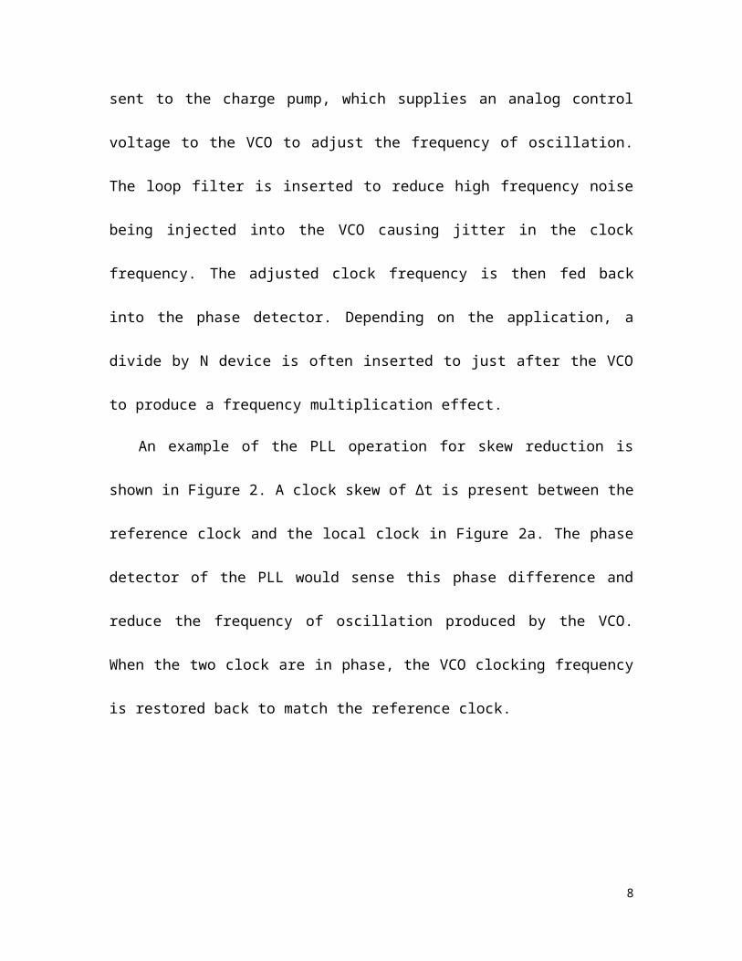
An example of the PLL operation for skew reduction is shown in Figure 2. A clock
skew of Δt is present between the reference clock and the local clock in Figure 2a. The
phase detector of the PLL would sense this phase difference and reduce the frequency of
oscillation produced by the VCO. When the two clock are in phase, the VCO clocking
frequency is restored back to match the reference clock.
Figure 2 – (a) Two clock with a skew, (b) change of clock frequency to eliminate skew
7
Chapter 3 - Voltage Controlled Oscillator
The voltage controller oscillator (VCO) is one of the key analog components inside
the PLL. It is responsible for synthesizing a frequency depending on the control voltage
sent from the charge pump. Several criteria must be met for the VCO to ensure good
performance for the PLL [2]. First, the VCO should have low phase noise, also called
jitter. Jitter is a variation of the excess phase in time. It is highly undesirable because it
shortens the eyediagram and lowers the time available for logic computation. Second, the
VCO should have large tuning range. Depending on the application, the PLL may be
required to output wide range of oscillation frequency. For instance, the 1394b Firewire
standard requires a receiver capable of supporting data rate from 100Mb/s to 1.6Gb/s.
Third, the VCO should have good tuning linearity over the tuning range because non-
linearity degrades the settling behavior of PLL’s.
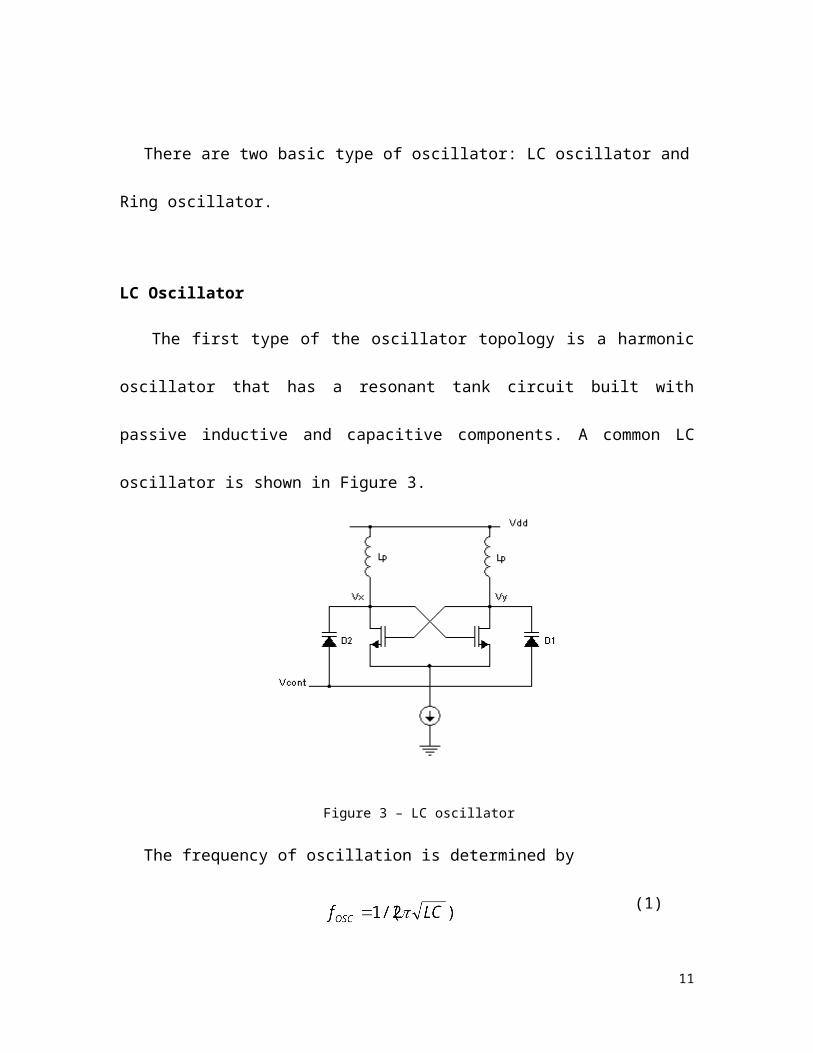
There are two basic type of oscillator: LC oscillator and Ring oscillator.
LC Oscillator
The first type of the oscillator topology is a harmonic oscillator that has a resonant
tank circuit built with passive inductive and capacitive components. A common LC
oscillator is shown in Figure 3.
8
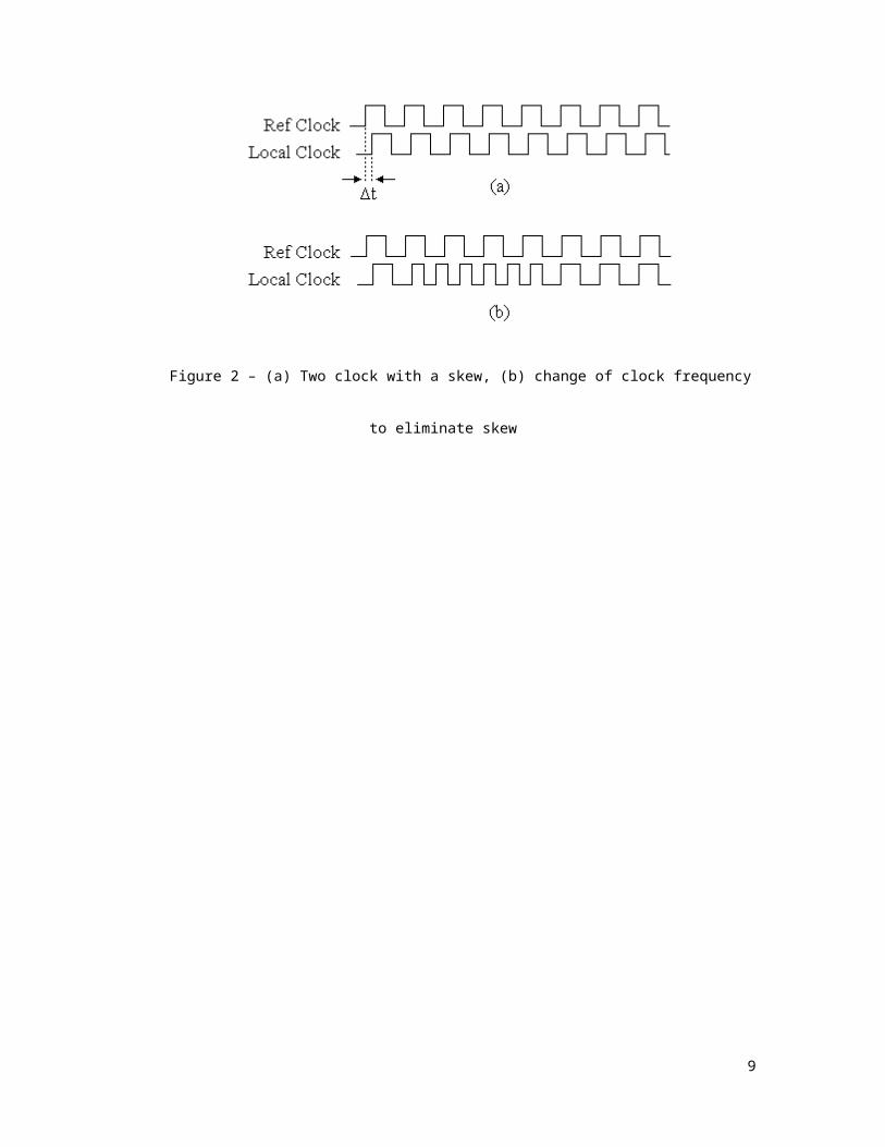
Figure 3 – LC oscillator
The frequency of oscillation is determined by
(1)
, where the capacitance is derived from the varactor diode D1 and D2 and can be changed
by setting the Vcont to vary the voltage drop across the varactor.
The LC oscillator inherently has low phase noise due to the frequency selectivity of
the resonator tank. However, the varactor diode has limited tuning range of less than
10%. Moreover, the central frequency of the LC oscillator is highly dependant on the
parasitic capacitance and the resistance of the inductor which vary depending on the
process variation and temperature. Lastly, monolithic inductor requires large area and
may be costly. Therefore for monolithic process, LC oscillator is not suited for
application in PLL design.
9

Ring Oscillator
The second type of the oscillatory topology is the ring oscillator. A ring oscillator
consists of a number of gain stages (or delay cells) in a loop (Figure 4a).
Figure 4 – (a) Three-Stage Ring Oscillator, (b) Differential Amplifier as a gain stage
The general formula for the close loop gain is Acl (jw) = A / (1- A·B(jw)). From the
Barkhausen Criteria, the system will produce a sustained oscillation if the loop gain
A·B(jw) satisfies the following two conditions:
| A·B(jw)| ≥ 1 (2)
∠ (A·B(jw)) = 180º (3)
Ideally, a ring oscillator with 2 gain stage and an ideal inverter will cause oscillation
if each gain stage displaces an ideal low pass characteristic with a phase drop of 90º.
However, in reality, to ensure proper feedback, 3 gain stages must be provided. The
frequency of the ring oscillator can be expressed as
10
(4)
, where N is the number of stages, TD is the large signal delay of each stage.
The advantage of the ring oscillator is that the gain stage can be easily realized by a
differential amplifier (Figure 4b) using the standard CMOS process. The oscillation
frequency can be set by varying the gain of each stage by adjusting the supply current.
Wide-range tuning can be achieved than compared to the LC oscillator. However, because
the ring oscillator lacks passive resonant components, it has much higher phase noise
than the LC oscillator. Thus the noise analysis has been an active topic in some papers
[3].
11

Schmitt Positive-Feedback Oscillator
Figure 5 – (a) Conventional delay cell, (b) SPFB delay cell
Figure 5a demonstrates a conventional gain stage that utilizes a differential amplifier
with triode-based loads for the ring oscillator. The operating frequency can be set by VGP
and tuned by varying VGN. This configuration suffers two draw back at low supply
voltage. First, the frequency dependence on the control voltage is non-linear. Second,
when VGN is near the threshold of the NMOS, the output voltage amplitude is too small
to drive the next stage (Figure 6).
Therefore a second configuration is proposed by Jung et al. [4] to achieve low
voltage VCO (Figure 5b). A Schmitt positive feedback (SPFB) is added as a slave
amplifier to the conventional gain stage. This generates a hysteresis window that
introduces an additional delay to the term TD in equation (4). Thus, once VGP and VGN
12

are set, the oscillation frequency can be obtained by varying VCTRL.
A 1.2GHz PLL with 1.5V supply voltage was constructed with this VCO topology
by 0.35μm TSMC CMOS technology. A total power dissipation of 10mW was achieved.
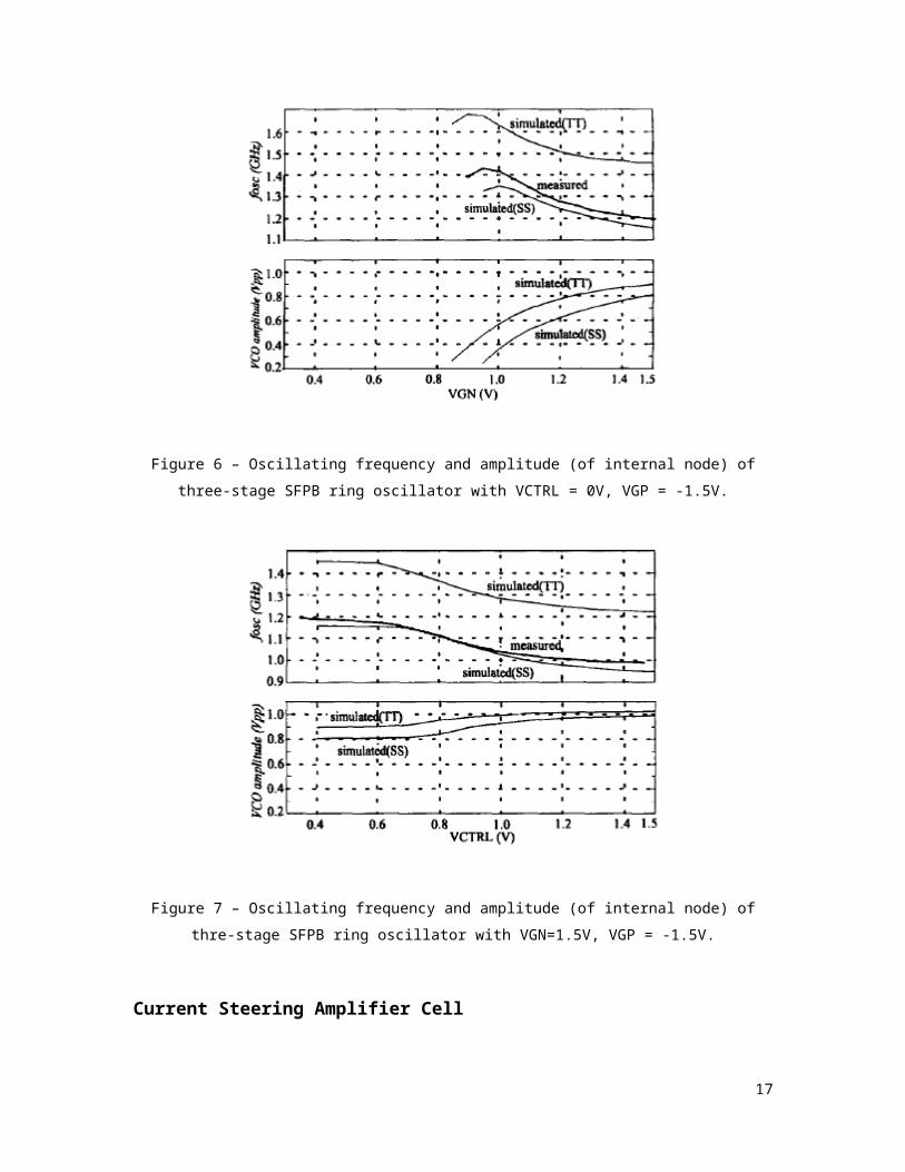
Figure 7 depicted the test result of the SPFB oscillator. The relationship between
Vctrl and the frequency is much more linear than the conventional delay cell. The output
amplitude is also kept constant at around 1.0V for entire tuning range.
Figure 6 – Oscillating frequency and amplitude (of internal node) of three-stage SFPB ring oscillator with
VCTRL = 0V, VGP = -1.5V.
13

Figure 7 – Oscillating frequency and amplitude (of internal node) of thre-stage SFPB ring oscillator with
VGN=1.5V, VGP = -1.5V.
Current Steering Amplifier Cell
Another technique for achieve low voltage design, a current-steering amplifier
(CSA) cell ring oscillator, is proposed by Yang et al. [5] and adopted by Pialis [6].
Figure 8 – (a) Current Steering Amplifier Cell, (b) VCO using a three-stage CSA ring oscillator
14

Figure 8a demonstrates a CSA cell. The NMOS M1 acts as the input device while
diode-connected NMOS M2 serves as the load. When compared to the conventional
differential pair amplifier in Figure 4b, it can be shown that given the same current source
configuration, the output swing of the differential pair amplifier is one Veff less than the
output swing of the CSA cell. Therefore the CSA cell can operate with much lower
supply voltage than the conventional differential amplifier.
The operation of the CSA cell is as follows. When Vin is high, M1 turns on, sinking
the bias current Ib and turning off M2. The on resistance of M1 then defines the output
low voltage, VOL. When Vin is low, M1 turns off and Ib is steered to M2. At this condition,
the on resistance of M2 defines the output high voltage VOH. Thus the signal output swing
can be found to be
(5)
From equation (5) illustrates that as Ib increases to increase the frequency, the output
swing also increases. This is a desirable feature because the signal level improves at high
frequency when the power supply switching noise becomes worse.
Using this technique, the paper in [6] has achieved a PLL with wide-tuning range of
0.3-165MHz and 0.3-100MHz at 5V and 3V supplies using standard 0.8μm n-well
15

CMOS process (Figure 9). The paper in [5] has demonstrated through simulation a
nominal 1V VCO with digital tenability from 115MHz to 185MHz using TSMC 0.18μm
technology. The power dissipation was 5.2mW at the center frequency 176MHz
Figure 9 – Measure VCO Performance for [6].
16
Chapter 4 - Charge Pump
Basic Structure
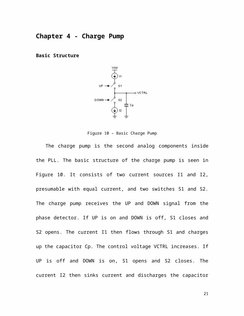
Figure 10 – Basic Charge Pump
The charge pump is the second analog components inside the PLL. The basic
structure of the charge pump is seen in Figure 10. It consists of two current sources I1
and I2, presumable with equal current, and two switches S1 and S2. The charge pump
receives the UP and DOWN signal from the phase detector. If UP is on and DOWN is off,
S1 closes and S2 opens. The current I1 then flows through S1 and charges up the
capacitor Cp. The control voltage VCTRL increases. If UP is off and DOWN is on, S1
opens and S2 closes. The current I2 then sinks current and discharges the capacitor Cp.
The control voltage VCTRL decreases. If both UP and DOWN are off, the control voltage
on the capacitor is maintained. The control voltage is then sent to the VCO to control its
output frequency.
17

Voltage Doubler Scheme
Figure 11 – PLL with Voltage Doubler inserted
As discussed previously, decrease in the power supply reduces the tuning range of the
PLL. To overcome this problem, another PLL scheme is proposed by Hung et al. that
inserts a voltage doubler and a level shifter before the charge pump (Figure 11) [7].
The voltage doubler inherently has switching noise and can not be applied directly to
the VCO. However, the charge pump does not have this issue due to its high supply
rejection ratio. The low pass capacitor Cp also helps filter out the voltage ripple from the
voltage doubler.
With this scheme, the paper in [7] has achieved a 1.5V 5.5GHz CMOS PLL
implemented in a 0.25μm foundry digital CMOS process. The tuning range is 285MHz
with utilization of a voltage doubler (Figure 12). The overall power dissipation is 23mW.
18

Figure 12 – A PLL frequency tuning characteristics utilizing the voltage doubler
19

Conclusion
Phase-Locked Loop is an important analog building block that has many
applications. The overall performance of the PLL suffers from the trend toward the
reduction in the supply voltage. As a result, the limitation in the output voltage headroom
reduces the tuning range of the PLL. Three schemes are discussed to improve the
situation. The first scheme utilizes a Schmitt Positive-Feedback Oscillator in the VCO
Ring Oscillator topology. This scheme maintains the output voltage level of the Ring
Oscillator and improves the linearity of the frequency over the tuning range. A second
scheme replaces the differential amplifier of the Ring Oscillator with a current-steering
amplifier in the VCO. This scheme increases the maximum output voltage swing to
improve the tuning range. The third technique of improving the tuning range utilizes the
voltage doubler to increase the supply voltage of the charge pump. The charge pump has
high supply noise rejection so the switching noise from the voltage doubler has minimum
effect.
20
Reference
1. Jan. M. Rabaey, “Digital Integrated Circuits”, Prentice Hall, 19962. Behzad Razavi, “Design of Analog CMOS Integrated Circuits”, McGraw Hill, 20013. T. C. Weigandt, B. Kim, P. R. Gray, “Analysis of Timing Jitter in CMOS ring
oscillator”, Proc. Of ISCAS, June 19944. D. C. Jung, D. S. Chen, J. M. Shyu, C. Y. Wu, “A Low-Power 1.2GHz 0.35um CMOS
PLL”, The Second IEEE Asia Pacific Conference on ASICs, pp 99-102, August 20025. Tony Pialis, Design and Analysis Techniques for Low-Voltage, Low Jitter Voltage-
Controlled Oscillators. M. A. Sc Dissertation, University of Toronto, Toronto, 20026. H. C. Yang, L. K. Lee, R. S. Co, “A Low Jitter 0.3-165 MHz CMOS PLL Frequency
Synthesizer for 3V/5V Operation”, IEEE Journal of Solid State, vol 32, pp. 582-586, April 1997
7. C. M. Hung and Kenneth K. O., “A Fully Integrated 1.5V 5.5GHz CMOS Phase-Locked Loop”, IEEE Journal of Solid-State Circuits, vol 27, pp. 521-525, Aril 2002
8. V. R. von Kaenel, “A High-Speed, Low-Power Clock Generator for a Microprocessor Application”, IEEE Journal of Solid-State Circuits, vol 33, pp. 1634-1639, November 1998
9. J. Savoj, B. Razavi, “A 10Gbs CMOS Clock and Data Recovery Circuit”, 2000 Symposium on VLSI Circuits Digest of Technical Papers, pp. 136-139, 2000
10. S. Lo, C. Olgaard, D. Rose, “A 1.8V/3.5mA 1.1GHz/300MHz CMOS Dual PLL Frequency Synthesizer IC for RF Communications”, IEEE 1998 Custom Integrated Circuits Conference, pp 571-574, 1998
21