Embed Size (px)
Citation preview

Optics Communications 285 (2012) 4372–4375
Contents lists available at SciVerse ScienceDirect
Optics Communications
0030-40
http://d
n Corr
Concord
E-m
journal homepage: www.elsevier.com/locate/optcom
Linewidth enhancement factor of InAs/InP quantum dot lasersaround 1.5 mm
Z.J. Jiao a,b,n, Z.G. Lu a, J.R. Liu a, P.J. Poole a, P.J. Barrios a, D. Poitras a, G. Pakulski a,J. Caballero a, X.P. Zhang b
a Institute for Microstructural Sciences, National Research Council, Ottawa, ON, Canadab Department of Electrical & Computer Engineering, Concordia University, Montreal, QC, Canada
a r t i c l e i n f o
Article history:
Received 4 July 2011
Accepted 2 July 2012Available online 17 July 2012
Keywords:
InAs/InP quantum dot lasers
Linewidth enhancement factor
Injection locking technique
Hakki–Paoli method
18/$ - see front matter & 2012 Elsevier B.V. A
x.doi.org/10.1016/j.optcom.2012.07.002
esponding author at: Department of Electric
ia University, Montreal, QC, Canada.
ail address: [email protected] (Z.J. Jiao).
a b s t r a c t
Linewidth enhancement factor (LEF) of InAs/InP quantum dot (QD) multi-wavelength lasers (MWLs)
emitting around 1.5 mm is investigated both above and below the threshold. Above the threshold, LEFs
at three different wavelengths around the gain peak of 1.53 mm by the injection locking technique are
obtained to be 1.63, 1.37 and 1.59. Then by Hakki–Paoli method LEF is found to decrease with increased
current and shows a value of less than 1 below the threshold. These small LEF values have clearly
indicated that our developed InAs/InP QDs are perfect and promising gain materials for QD MWLs, QD
mode-locked lasers (QD MLLs) and QD distributed-feedback (QD DFB) lasers around 1.5 mm.
& 2012 Elsevier B.V. All rights reserved.
1. Introduction
The concept of quantum dots (QDs) was proposed by Arakawaet al. in 1982 for application to semiconductor lasers with thetheoretical prediction of temperature-insensitive threshold cur-rent characteristics [1]. Most of the significant characteristics ofQD lasers were demonstrated, including low- and temperature-insensitive threshold current, fast recovery time, enhanced mod-ulation bandwidth and small linewidth enhancement factor [2,3].The linewidth enhancement factor (LEF) a is one of the mostimportant factors in semiconductor lasers including QD lasers. Itdetermines fundamental properties of QD lasers, such as line-width, filamentation in high power lasers [4], feedback sensitivity[5], frequency chirping and time jittering of mode-lockedlasers [6]. The LEF parameter can be measured by the methodsof Hakki–Paoli (H–P) [7] and injection locking [8]. Small LEFvalues of less than 1 in QD lasers and semiconductor opticalamplifiers (SOAs) emitting at around 1.3 mm have been obtained[9–11], which are based on the material of InAs/GaAs QDs. Toreach the most important 1.5 mm wavelength range for telecom-munication applications, in the past years we have put greatefforts to develop InAs/InP-based QD gain materials to realize QDlasers [12,13] and semiconductor optical amplifiers (SOAs) [14]around 1.5 mm. However only two research groups have reported
ll rights reserved.
al & Computer Engineering,
their experiments to quantify LEF values of GaAs/InP QD lasers,which are in the range from 2.2 to 7.6 [15,16].
In this paper, LEF parameter of an InAs/InP QD multi-wave-length laser (QD-MWL) with a centre wavelength of 1.53 mm isinvestigated for the first time. The injection locking technique isused to evaluate the above-threshold LEF. LEF can be directlydeduced from the positive and the negative locking bandwidthswithout other fitting parameters. The LEF is found to be only 1.37at a gain peak of 1.53 mm. Then the result is confirmed by the H–Pmethod which shows a reduced LEF of less than 1 just belowthreshold. The measured small LEF values have indicated that ourdeveloped InAs/InP QD gain materials will lead an ultra-narrowlinewidth of QD DFB lasers [17], with much less sensitivity of QDMWLs [18] to optical feedback [19], and also lead to a lowerfrequency chirp and time jitter of QD mode-locked lasers (QD-MLLs) [20,21] which are suitable for very high data rate transmis-sion networking systems [22].
2. Experimental setup, results and discussions
The InAs/InP QD laser samples used in this study weregrown by chemical beam epitaxy (CBE) on exactly (100) orientedn-type InP substrates. The undoped active region of theQD sample consisted of five stacked layers of InAs QDs withIn0.816Ga0.184As0.392P0.608 (1.15 Q) barriers. The QDs were tuned tooperate in the desirable operation wavelength range by using aQD double cap growth procedure and a GaP sublayer [23]. In thedouble cap process the dots are partially capped with a thin layerof barrier material, followed by a 30 s growth interruption and

Z.J. Jiao et al. / Optics Communications 285 (2012) 4372–4375 4373
then complete capping. The thickness of the partial cap controlsthe height of the dots, and hence their emission wavelength. Italso helps control the height distribution of the dots, and there-fore control the 3 dB spectral bandwidth of the gain spectrum.Growing the dots on a thin GaP layer allows a high dot densityand improves layer uniformity when stacking multiple layers ofdots, providing maximum gain. This active layer was embeddedin a 355 nm thick 1.15 Q waveguiding core, providing both carrierand optical confinement. An average dot density of approximately4�1010 cm�2 per layer was obtained according to our atomicforce microscopy (AFM) measurement on uncapped stacked dotsamples. The waveguiding core was surrounded by p-doped (top)and n-doped (bottom) layers of InP and capped with a heavilydoped thin InGaAs layer to facilitate the fabrication of lowresistance Ohmic contacts. The sample was fabricated into singlelateral mode ridge waveguide lasers with a ridge width of 3 mm,and then cleaved to form a Fabry–Perot (F–P) laser cavity. Thelaser was driven with a DC injection current, and tested on a heatsink maintained at 18 1C. The threshold current is 45.5 mA undercontinuous-wave (CW) operation. Fig. 1 shows the typical spec-trum of a C-band QD MWL with an injection current of 60 mA.The experimental setup used in the LEF measurement by theinjection locking method is shown in Fig. 2. A tunable laser(Agilent 8164B) that worked as the master laser (ML) was usedto lock the QD MWL (slave laser). The ML had a wavelength
Fig. 1. Typical spectrum of an InAs/InP QD multi-wavelength laser with the
injection current of 60 mA at 18 1C.
Masterlaser
Polarizationcontroller
QDMWL
OSA
50:50coupler
Powermeter
Lensed fiber
PM circulator
Fig. 2. Schematic diagram of measuring the LEF factor using the injection locking
method.
accuracy of 0.1 pm. Output light from the ML was injected intothe slave laser (SL) through one port of a polarization-maintaining(PM) circulator. A single mode lensed fiber was used to lead lightfrom the ML into the SL as well as receive light from the SL afterlocking. The PM circulator ensured the light transmission in onlyone direction. A power meter (Newport 840) and a high resolu-tion (10 pm) optical spectrum analyzer (OSA) (Ando AQ6317B)were connected to two ports of a 3 dB coupler to monitor thepower and the spectrum at the same time.
When light from the ML is injected into the QD MWL, i.e. theSL, the injected light competes with all longitudinal modes of theSL. At the locked state, the SL emits at the injected wavelength ofthe ML while the gain at other wavelengths is highly suppressed.The locking and unlocking conditions are dependent on power ofthe injected light as well as frequency detuning from the closestlongitudinal mode of the SL. The locking bandwidth is given bythe formula [24]
�rffiffiffiffiffiffiffiffiffiffiffiffiffi1þa2
p¼DonegativeoDooDopositive ¼ r ð1Þ
where r¼ ðc=2nlÞðPi=PÞ1=2 is the injection rate, Pi is the injectedpower from ML, P is the power of the SL, n is the refractive indexand a is the LEF of the SL. Locking is achieved within the detuningrange given in Eq. (1). It is obvious that the positive and negativelocking range is asymmetric, which can be used to calculate theLEF value. It is given by [24]
a¼
ffiffiffiffiffiffiffiffiffiffiffiffiffiffiffiffiffiffiffiffiffiffiffiffiffiffiffiffiffiffiffiffiffiffiffiffiffiDonegative
Dopositive
� �2
�1
sð2Þ
In the experiment, the SL was pumped by a CW injection currentof 60 mA and the temperature was controlled at 18 1C. Threedifferent wavelengths at 1524.24 nm, 1529.53 nm and 1535.52 nmwere selected to measure the LEF which covers the main gainregion as shown in Fig. 1. The locking condition was reachedwhen at least 30 dB side-mode suppression ratios were observedon the OSA for each injected power. The detuning frequency atboth positive and negative sides increased with injected power ofthe ML as shown in Fig. 3. By linear fitting, the LEF was calculatedas the ratio of the two slopes of detuning ranges [8] using Eq. (2).The LEF values at the three wavelengths are 1.63, 1.37 and 1.59.To our best knowledge, these are the lowest values reported so farfor QD lasers emitting around 1.5 mm based on the substrateof InP.
The LEF obtained by the injection locking technique is areflection of the laser’s working performance at lasing while theH–P method is the one to know the key properties of lasers. Inorder to remove the influence of heating to the change ofrefractive index, a pulse generator (Agilent 8114A) was taken toprovide pulsed current. A pulse width of 400 ns and a duty cycleof 2.5% were used in the experiment. In this method, the LEF iscalculated as [7]
a¼ �4pl
dn=dN
dg=dN¼�4pn
l2
dl=dN
dg=dNð3Þ
where n is the refractive index, g is the net modal gain, and N isthe carrier density. It shows the relationship between change ofrefractive index and gain caused by the variation of carrierdensity in the active region. The net modal gain is given byg ¼ ð1=LÞInð
ffiffiffiffiffiffiffiffiffir�1p
=ffiffiffiffiffiffiffiffiffiffirþ1p
Þ, where L is the cavity length and r is thepeak to valley ratio of each longitudinal mode in amplifierspontaneous emission (ASE) spectrum of the QD MWL.
And the refractive index change can be obtained by measuringthe frequency shift of each peak in the ASE spectrum. Underpulsed condition, output power is low below threshold; henceonly 1 nm of the ASE spectrum around the gain peak wasanalyzed to obtain gain and wavelength shift. Three peaks were
-10-8-6-4-20246
detu
ning
freq
uenc
y (G
Hz)
detu
ning
freq
uenc
y (G
Hz)
Pin(mW)1/2 Pin(mW)1/2 Pin(mW)1/2
1524.24nm
-10-8-6-4-20246 1529.53nm
-10-8-6-4-20246
detu
ning
freq
uenc
y (G
Hz) 1535.52 nm
1.81.0 1.2 1.4 1.6 1.81.0 1.2 1.4 1.6 2.01.0 1.2 1.4 1.6 1.8
Fig. 3. Positive detuning and negative detuning as function of square root of injected power from the ML at three different wavelengths. The solid lines are linear fitting of
experimental results.
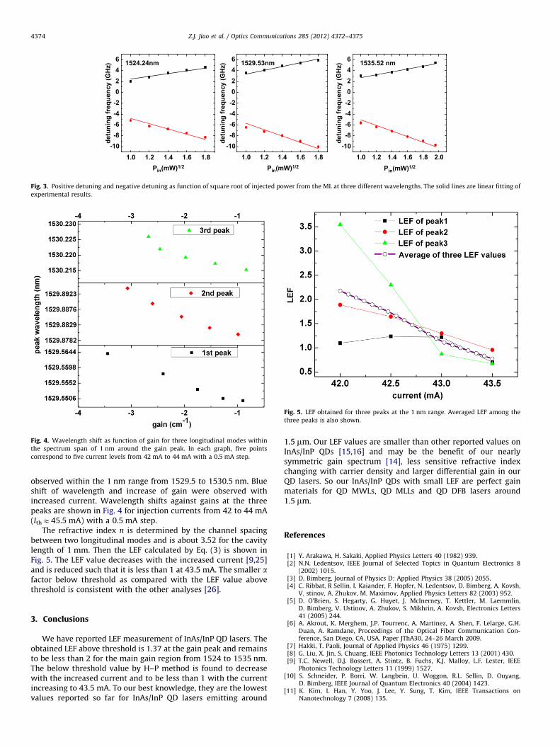
Fig. 4. Wavelength shift as function of gain for three longitudinal modes within
the spectrum span of 1 nm around the gain peak. In each graph, five points
correspond to five current levels from 42 mA to 44 mA with a 0.5 mA step.
Fig. 5. LEF obtained for three peaks at the 1 nm range. Averaged LEF among the
three peaks is also shown.
Z.J. Jiao et al. / Optics Communications 285 (2012) 4372–43754374
observed within the 1 nm range from 1529.5 to 1530.5 nm. Blueshift of wavelength and increase of gain were observed withincreased current. Wavelength shifts against gains at the threepeaks are shown in Fig. 4 for injection currents from 42 to 44 mA(IthE45.5 mA) with a 0.5 mA step.
The refractive index n is determined by the channel spacingbetween two longitudinal modes and is about 3.52 for the cavitylength of 1 mm. Then the LEF calculated by Eq. (3) is shown inFig. 5. The LEF value decreases with the increased current [9,25]and is reduced such that it is less than 1 at 43.5 mA. The smaller afactor below threshold as compared with the LEF value abovethreshold is consistent with the other analyses [26].
3. Conclusions
We have reported LEF measurement of InAs/InP QD lasers. Theobtained LEF above threshold is 1.37 at the gain peak and remainsto be less than 2 for the main gain region from 1524 to 1535 nm.The below threshold value by H–P method is found to decreasewith the increased current and to be less than 1 with the currentincreasing to 43.5 mA. To our best knowledge, they are the lowestvalues reported so far for InAs/InP QD lasers emitting around
1.5 mm. Our LEF values are smaller than other reported values onInAs/InP QDs [15,16] and may be the benefit of our nearlysymmetric gain spectrum [14], less sensitive refractive indexchanging with carrier density and larger differential gain in ourQD lasers. So our InAs/InP QDs with small LEF are perfect gainmaterials for QD MWLs, QD MLLs and QD DFB lasers around1.5 mm.
References
[1] Y. Arakawa, H. Sakaki, Applied Physics Letters 40 (1982) 939.[2] N.N. Ledentsov, IEEE Journal of Selected Topics in Quantum Electronics 8
(2002) 1015.[3] D. Bimberg, Journal of Physics D: Applied Physics 38 (2005) 2055.[4] C. Ribbat, R Sellin, I. Kaiander, F. Hopfer, N. Ledentsov, D. Bimberg, A. Kovsh,
V. stinov, A. Zhukov, M. Maximov, Applied Physics Letters 82 (2003) 952.[5] D. O’Brien, S. Hegarty, G. Huyet, J. McInerney, T. Kettler, M. Laemmlin,
D. Bimberg, V. Ustinov, A. Zhukov, S. Mikhrin, A. Kovsh, Electronics Letters41 (2005) 244.
[6] A. Akrout, K. Merghem, J.P. Tourrenc, A. Martinez, A. Shen, F. Lelarge, G.H.Duan, A. Ramdane, Proceedings of the Optical Fiber Communication Con-ference, San Diego, CA, USA, Paper JThA30, 24–26 March 2009.
[7] Hakki, T. Paoli, Journal of Applied Physics 46 (1975) 1299.[8] G. Liu, X. Jin, S. Chuang, IEEE Photonics Technology Letters 13 (2001) 430.[9] T.C. Newell, D.J. Bossert, A. Stintz, B. Fuchs, K.J. Malloy, L.F. Lester, IEEE
Photonics Technology Letters 11 (1999) 1527.[10] S. Schneider, P. Borri, W. Langbein, U. Woggon, R.L. Sellin, D. Ouyang,
D. Bimberg, IEEE Journal of Quantum Electronics 40 (2004) 1423.[11] K. Kim, I. Han, Y. Yoo, J. Lee, Y. Sung, T. Kim, IEEE Transactions on
Nanotechnology 7 (2008) 135.

Z.J. Jiao et al. / Optics Communications 285 (2012) 4372–4375 4375
[12] G. Ortner, C.Ni. Allen, C. Dion, P. Barrios, D. Poitras, D. Dalacu, G. Pakulski,J. Lapointe, P.J. Poole, W. Render, S. Raymond, Applied Physics Letters 88(2006) 121119.
[13] J.R. Liu, Z.G. Lu, S. Raymond, P.J. Poole, P.J. Barrios, D. Poitras, IEEE PhotonicsTechnology Letters 20 (2008) 81.
[14] Z.G. Lu, J.R. Liu, S. Raymond, P.J. Poole, P.J. Barrios, G. Pakulski, D. Poitras, F.G. Sun,S. Taebi, T.J. Hall, Proceedings of the Optical Fiber Communication Conference,OFC’2007, Anaheim, California, USA, Paper JThA33, 25–29 March 2007.
[15] F. Lelarge, B. Rousseau, B. Dagens, F. Poingt, F. Pommereau, A. Accard, IEEEPhotonics Technology Letters 17 (2005) 1369.
[16] F. Grillot, A. Martinez, K. Merghem, J. Provost, F. Alexandre, R. Piron, O.Dehaese, S. Loualiche, L. Lester, A. Ramdane, Proceedings of the 21st AnnualMeeting of the IEEE Lasers and Electro-Optics Society, Newport Beach, CA,November 2008.
[17] Z.G. Lu, P.J. Poole, J.R. Liu, P.J. Barrior, Z.J. Jiao, G. Pakulski, D. Poitras,D. Goodchild, B. Rioux, A.J. SpringThorpe, Electronics Letters 47 (2011) 818.
[18] Z.G. Lu, J.R. Liu, P.J. Poole, S. Raymond, P.J. Barrios, D. Poitras, G. Pakulski, X.P.Zhang, K. Hinzer, T.J. Hall, Proceedings of the Optical Fiber CommunicationConference, San Diego, CA, USA, Paper JWA27, 24–26 March 2009.
[19] S. Azouigui, B. Dagens, F. Lelarge, J.G. Provost, D. Make, O.L. Gouezigou,A. Accard, A. Martinez, K. Merghem, F. Grillot, O. Dehaese, R. Piron,S. Loualiche, Q. Zou, A. Ramdane, IEEE Journal of Selected Topics in Quantum
Electronics 15 (2009) 764.[20] Z.G. Lu, J.R. Liu, P.J. Poole, Z.J. Jiao, P.J. Barrios, D. Poitras, J. Caballero,
X.P. Zhang, Optics Communications 284 (2011) 2323.[21] Z.G. Lu, J.R. Liu, P.J. Poole, S. Raymond, P.J. Barrios, D. Poitras, G. Pakulski,
P. Grant, D. Roy-Guay, Optics Express 17 (2009) 13609.[22] H. Schmeckebier, G. Fiol, C. Meuer, D. Arsenijevic, D. Bimberg, Optics Express
18 (2010) 3415.[23] P.J. Poole, K. Kaminska, P. Barrios, Z.G. Lu, J.R. Liu, Journal of Crystal Growth
311 (2009) 1482.[24] I. Petitbon, P. Gallion, G. Debarge, C. Chabran, IEEE Journal of Quantum
Electronics 24 (1988) 148.[25] A. Martinez, A. Lemaı̂tre, K. Merghem, L. Ferlazzo, C. Dupuis, A. Ramdane, J.-
G. Provost, B. Dagens, O. Le Gouezigou, O. Gauthier-Lafaye, Applied PhysicsLetters 86 (2005) 211115.
[26] S. Melnik, G. Huyet, Optics Express 14 (2006) 2950.


![Karimi understanding lasers[1]](https://img.pdfslide.tips/doc/110x75/587df0b41a28abab7e8b4bfd/karimi-understanding-lasers1.jpg)