Embed Size (px)
Citation preview
7/28/2019 LM339 LM239 LM2901 Datasheet
http://slidepdf.com/reader/full/lm339-lm239-lm2901-datasheet 1/8
ww w.fa irchilds e mi.com
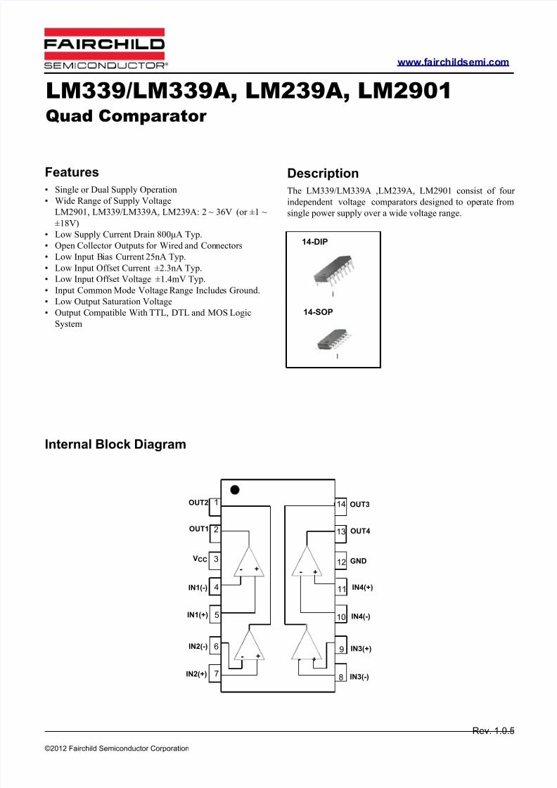
LM339/LM339A, LM239A, LM2901Quad Comparator
Features
• Single or Dual Supply Operation
• Wide Range of Supply Voltage
LM2901, LM339/LM339A, LM239A: 2 ~ 36V (or ±1 ~
±18V)
• Low Supply Current Drain 800μA Typ.
• Open Collector Outputs for Wired and Connectors
• Low Input Bias Current 25nA Typ.
• Low Input Offset Current ±2.3nA Typ.
• Low Input Offset Voltage ±1.4mV Typ.• Input Common Mode Voltage Range Includes Ground.
• Low Output Saturation Voltage
• Output Compatible With TTL, DTL and MOS Logic
System
Description
The LM339/LM339A ,LM239A, LM2901 consist of four
independent voltage comparators designed to operate from
single power supply over a wide voltage range.
14-DIP
1
14-SOP
1
Internal Block Diagram
OUT2 1
OUT1 2
14 OUT3
13 OUT4
VCC 3
- +12 GND
- +
IN1(-) 4
IN1(+) 5
IN2(-) 6
- +
IN2(+) 7
11 IN4(+)
10 IN4(-)
9 IN3(+)
- +
8 IN3(-)
Rev. 1.0.5
©2012 Fairchild Semiconductor Corporation
7/28/2019 LM339 LM239 LM2901 Datasheet
http://slidepdf.com/reader/full/lm339-lm239-lm2901-datasheet 2/8
LM339/LM339A, LM239A, LM2901
2
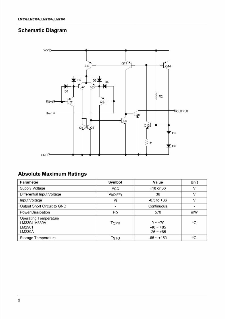
Schematic Diagram
VCC
Q12Q9 Q14
D2 D3D4
IN(+)
Q2 Q3
D1
R2
Q1 Q4
IN(-) OUTPUTQ8
Q5 Q6
Q7
Q13
D5
R1D6
GND
Absolute Maximum Ratings
Parameter Symbol Value Unit
Supply Voltage VCC ±18 or 36 V
Differential Input Voltage VI(DIFF) 36 V
Input Voltage VI -0.3 to +36 V
Output Short Circuit to GND - Continuous -
Power Dissipation PD 570 mW
Operating Temperature
LM339/LM339ALM2901
LM239A
TOPR 0 ~ +70-40 ~ +85
-25 ~ +85
°C
Storage Temperature TSTG -65 ~ +150 °C
7/28/2019 LM339 LM239 LM2901 Datasheet
http://slidepdf.com/reader/full/lm339-lm239-lm2901-datasheet 3/8
Electrical Characteristics
(VCC = 5V, T A = 25°C, unless otherwise specified)
Parameter Symbol ConditionsLM239A/LM339A LM339
Unit
Min. Typ. Max. Min. Typ. Max.Input Offset
VoltageVIO
VO(P) =1.4V, RS = 0Ω - 1 2 - 1.4 5 mV
Note1 - - 4.0 - - 9.0
Input Offset
CurrentIIO
IIN(+) - IIN(-), VCM = 0V - 2.3 50 - 2.3 50 nA
Note1 - - 150 - - 150
Input Bias Current IBIASVCM = 0V - 57 250 - 57 250
nANote1 - - 400 - - 400
Input Common
Mode Voltage
Range
VI(R)
VCC = 30V 0 - VCC-1.5 0 - VCC-1.5
VNote1 0 - VCC-2 0 - VCC-2
Supply Current ICC VCC = 5V, RL = ∞ - 1.1 2.0 - 1.1 2.0 mA
Voltage Gain GVVCC =15V, RL ≥ 15kΩ
(for large swing)50 200 - 50 200 - V/mV
Large Signal
Response TimeTLRES
VI = TTL Logic Swing
VREF = 1.4V, VRL = 5V,
RL = 5.1kΩ (Note2)
- 300 - - 300 - ns
Response Time TRESVRL = 5V, RL = 5.1kΩ
(Note2)- 1.3 - - 1.3 - μs
Output Sink
CurrentISINK
VI(-) ≥ 1V, VI(+) = 0V,
VO(P) ≤ 1.5V6 18 - 6 18 - mA
Output Saturation
Voltage VSAT
VI(-) ≥ 1V, VI(+) = 0V - 140 400 - 140 400
mVISINK = 4mA Note1 - - 700 - - 700
Output Leakage
CurrentIo(LKG)
VI(-) = 0V
VI(+) = 1V
VO(P) = 5V - 0.1 - - 0.1 - nA
VO(P) = 30V - - 1.0 - - 1.0 μ A
Differential Voltage VI(DIFF) Note1 - - 36 - - 36 V
Note:
1. LM339/LM339A : 0 ≤ T A ≤ +70°C
LM2901 : -40 ≤ T A ≤ +85°C
LM239A : -25 ≤ T A ≤ +85°C
2. These parameters, although guaranteed, are not 100% tested in production.
7/28/2019 LM339 LM239 LM2901 Datasheet
http://slidepdf.com/reader/full/lm339-lm239-lm2901-datasheet 4/8
Electrical Characteristics (Continued)
(VCC = 5V, T A = 25°C, unless otherwise specified)
Parameter Symbol ConditionsLM2901
Unit
Min. Typ. Max.
Input Offset Voltage VIOVO(P) =1.4V, RS = 0Ω - 2 7
mVNote1 - 9 15
Input Offset Current IIO- 2.3 50
nANote1 - 50 200
Input Bias Current IBIAS- 57 250 nA
Note1 - 200 500
Input Common
Mode Voltage
Range
VI(R)
LM2901, VCC =30V 0 - VCC-1.5
VNote1 0 - VCC-2
Supply Current ICC RL =∞, VCC=5V - 1.1 2.0 mARL =∞,VCC=30V - 1.6 2.5
Voltage Gain GVVCC =15V, RL ≥ 15kΩ
(for large swing)25 100 - V/mV
Large Signal
Response Time
TLRES VI =TTL Logic Swing
VREF =1.4V, VRL =5V, RL =5.1kΩ
(Note2)
- 300 -
ns
Response Time TRES VRL = 5V, RL = 5.1kΩ (Note2) - 1.3 - μs
Output Sink Current ISINK VI(-) ≥ 1V, VI(+) =0V, VO(P) ≤ 1.5V 6 18 - mA
Output Saturation
Voltage
VSATVI(-) ≥ 1V, VI(+) = 0V - 140 400
mV
ISINK =4mA Note1 - - 700Output Leakage
CurrentIO(LKG)
VI(-) = 0V VO(P) = 5V - 0.1 - nA
VI(+) = 1V VO P = 30V - - 1.0 μ A
Differential Voltage VI(DIFF) Note1 - - 36 V
Note:
1. LM339/LM339A : 0 ≤ T A ≤ +70°C
LM2901 : -40 ≤ T A ≤ +85°C
LM239A : -25 ≤ T A ≤ +85°C
2. These parameters, although guaranteed, are not 100% tested in production.
7/28/2019 LM339 LM239 LM2901 Datasheet
http://slidepdf.com/reader/full/lm339-lm239-lm2901-datasheet 5/8
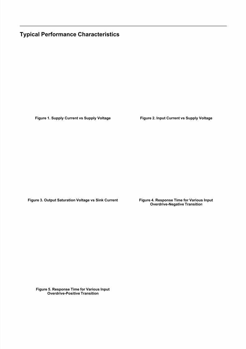
Typical Performance Characteristics
Figure 1. Supply Current vs Supply Voltage Figure 2. Input Current vs Supply Voltage
Figure 3. Output Saturation Voltage vs Sink Current Figure 4. Response Time for Various InputOverdrive-Negative Transition
Figure 5. Response Time for Various InputOverdrive-Positive Transition
7/28/2019 LM339 LM239 LM2901 Datasheet
http://slidepdf.com/reader/full/lm339-lm239-lm2901-datasheet 6/8
1 9 . 8
0
0 . 7
8 0
M A X
1 9 . 4
0 ± 0 . 2
0
0 . 7
6 4 ± 0 . 0
0 8
2 . 0
8
0 . 0
8 2
(
)
0 . 4
6 ± 0 . 1
0
0 . 0
1 8 ± 0 . 0
0 4
2 . 5
4
0 . 1
0 0
1 . 5
0 ± 0 . 1
0
0 . 0
5 9 ± 0 . 0
0 4
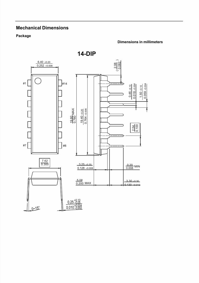
Mechanical Dimensions
Package
Dimensions in millimeters
14-DIP
6.40 ±0.20
0.252 ±0.008
#1 #14
#7 #8
7.62
0.300 3.25 ± 0.20
0.128 ±0.008
0.20
0.008MIN
5.08
0.200 MAX3.30 ± 0.30
0.130 ±0.012
7/28/2019 LM339 LM239 LM2901 Datasheet
http://slidepdf.com/reader/full/lm339-lm239-lm2901-datasheet 7/8
7/28/2019 LM339 LM239 LM2901 Datasheet
http://slidepdf.com/reader/full/lm339-lm239-lm2901-datasheet 8/8
© 2012 Fairchild Semiconductor Corporation
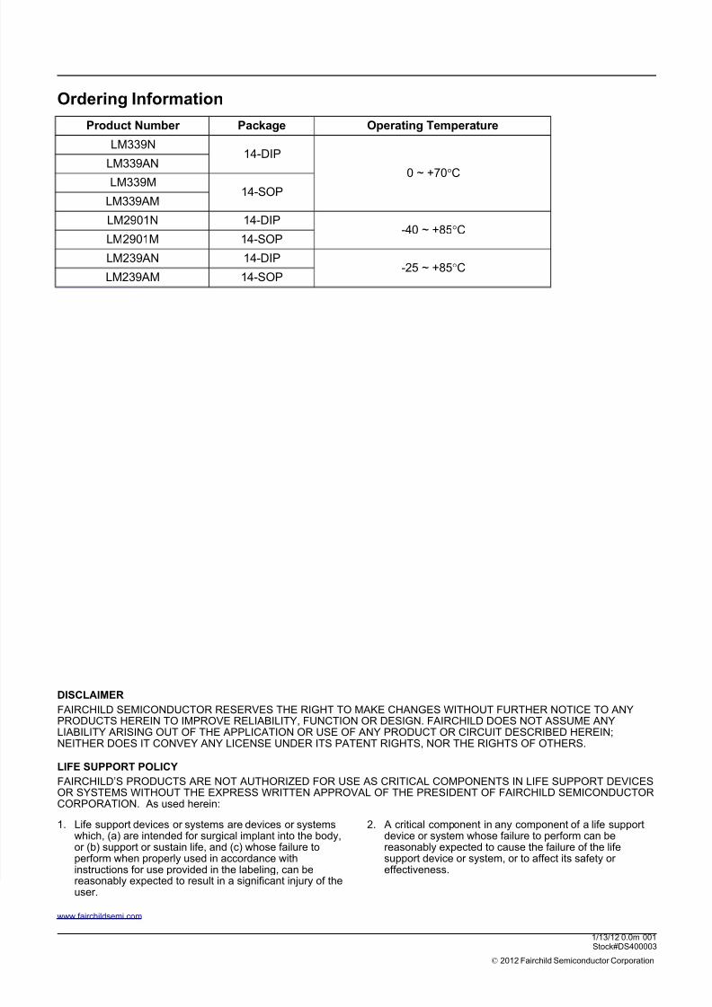
Ordering Information
Product Number Package Operating Temperature
LM339N14-DIP
0 ~ +70°
C
LM339AN
LM339M14-SOP
LM339AM
LM2901N 14-DIP-40 ~ +85°C
LM2901M 14-SOP
LM239AN 14-DIP-25 ~ +85°C
LM239AM 14-SOP
DISCLAIMER
FAIRCHILD SEMICONDUCTOR RESERVES THE RIGHT TO MAKE CHANGES WITHOUT FURTHER NOTICE TO ANYPRODUCTS HEREIN TO IMPROVE RELIABILITY, FUNCTION OR DESIGN. FAIRCHILD DOES NOT ASSUME ANYLIABILITY ARISING OUT OF THE APPLICATION OR USE OF ANY PRODUCT OR CIRCUIT DESCRIBED HEREIN;NEITHER DOES IT CONVEY ANY LICENSE UNDER ITS PATENT RIGHTS, NOR THE RIGHTS OF OTHERS.
LIFE SUPPORT POLICY
FAIRCHILD’S PRODUCTS ARE NOT AUTHORIZED FOR USE AS CRITICAL COMPONENTS IN LIFE SUPPORT DEVICESOR SYSTEMS WITHOUT THE EXPRESS WRITTEN APPROVAL OF THE PRESIDENT OF FAIRCHILD SEMICONDUCTORCORPORATION. As used herein:
1. Life support devices or systems are devices or systemswhich, (a) are intended for surgical implant into the body,or (b) support or sustain life, and (c) whose failure toperform when properly used in accordance withinstructions for use provided in the labeling, can be
reasonably expected to result in a significant injury of theuser.
2. A critical component in any component of a life supportdevice or system whose failure to perform can bereasonably expected to cause the failure of the lifesupport device or system, or to affect its safety or effectiveness.
www.fairchildsemi.com
1/13/12 0.0m 001Stock#DS400003