Embed Size (px)
Citation preview
LM5041B
www.ti.com SNVS605 –MAY 2009
LM5041B Cascaded PWM ControllerCheck for Samples: LM5041B
1FEATURES DESCRIPTIONThe LM5041B PWM controller contains all of the
2• Internal Start-up Bias Regulatorfeatures necessary to implement either current-fed or
• Programmable Line Under-Voltage Lockout voltage-fed push-pull or bridge power converters.(UVLO) with Adjustable Hysteresis These “Cascaded” topologies are well suited for
• Current Mode Control multiple output and higher power applications. TheLM5041B includes these four control outputs: the• Internal Error Amplifier with Referencebuck stage controls (HD and LD) and the push-pull
• Cycle-by-cycle Over-Current Protection control outputs (PUSH and PULL). Push-pull outputs• Leading Edge Blanking are driven at 50% nominal duty cycle at one half of
the switching frequency of the buck stage and can be• Programmable Push-Pull Overlap or Deadconfigured for either a specified overlap time (forTimecurrent-fed applications) or a specified non-overlap
• Internal 1.5A Push-Pull Gate Drivers time (for voltage-fed applications). Push-pull stage• Programmable Soft-Start MOSFETs can be driven directly from the internal
gate drivers while the buck stage requires an external• Programmable Oscillator with Sync Capabilitydriver such as the LM5102. The LM5041B includes a• Precision Reference high-voltage start-up regulator that operates over a
• Thermal Shutdown wide input range of 15V to 100V. The PWM controlleris designed for high-speed capability including anoscillator frequency range up to 1 MHz and totalAPPLICATIONSpropagation delays of less than 100 ns. Additional• Telecommunication Power Converters features include line Under-Voltage Lock-Out
• Industrial Power Converters (UVLO), Soft-Start, an error amplifier, precisionvoltage reference, and thermal shutdown.• Multi-Output Power Converters
The differences between LM5041, LM5041A andPACKAGES LM5041B are as follows: In the LM5041A and the
LM5041B version, the hiccup mode over-current• TSSOP-16protection is not employed and the VCC bias• WSON-16 (5x5 mm) Thermally Enhanced regulator is not disabled by a low state at the SS pin.In the LM5041B version, both the high and low sidebuck stage gate drivers are forced to a low statewhen the controller is disabled. In the LM5041 andthe LM5041B version, the buck stage controller isdisabled by either a low state at the UVLO pin or alow state at the SS pin. Also in the LM5041B version,the REF pin 5V regulator is not disabled by a UVLOpin low state.
1
Please be aware that an important notice concerning availability, standard warranty, and use in critical applications ofTexas Instruments semiconductor products and disclaimers thereto appears at the end of this data sheet.
2All trademarks are the property of their respective owners.
PRODUCTION DATA information is current as of publication date. Copyright © 2009, Texas Instruments IncorporatedProducts conform to specifications per the terms of the TexasInstruments standard warranty. Production processing does notnecessarily include testing of all parameters.
1
2
3
4
5
6
7
8 9
10
VIN
FB
COMP
VCC
UVLO
PGND
CS
RT
SS
11
12
13
14
15
16
REF
HD
LD
PUSH PULL
AGND
TIME
FEEDBACK
LM5102
PUSH
PULL
33V - 76V VOUT
HIVIN
LM5041B
VCC
HD
LD
FB
VDD
HB
LO
VSS
RT1
RT2
LI
RT2
HO
HS
LM5041B
SNVS605 –MAY 2009 www.ti.com
Typical Application Circuit
Figure 1. Simplified Cascaded Push-Pull Power Converter
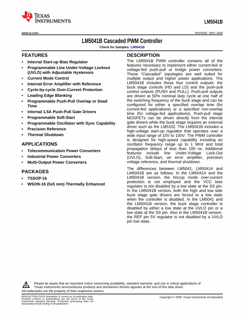
Connection Diagram
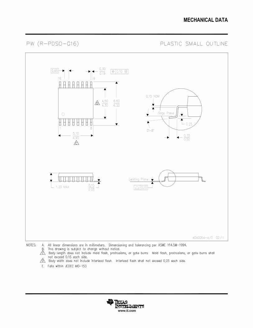
Figure 2. 16-Lead TSSOP, WSON
2 Submit Documentation Feedback Copyright © 2009, Texas Instruments Incorporated
Product Folder Links: LM5041B
LM5041B
www.ti.com SNVS605 –MAY 2009
PIN DESCRIPTIONSPin PinPin # Pin Application InformationName Description
1 VIN Source Input Voltage Input to start-up regulator. Input range 15V to 100V.
Inverting input for the internal error amplifier. The non-inverting input is connected to a2 FB Feedback Signal 0.75V reference.
Output of the Internal There is an internal 5 kΩ resistor pull-up on this pin. The error amplifier provides an3 COMP Error Amplifier active sink.
Precision 5 volt Maximum output current: 10 mA. Locally decouple with a 0.1 µF capacitor. Reference4 REF reference output stays low until the VCC UV are satisfied.
Buck switch PWM control output. The maximum duty cycle clamp for this outputMain Buck PWM5 HD corresponds to an off time of typically 240 ns per cycle. The LM5101 or LM5102 Buckcontrol output stage gate driver can be used to level shift and drive the Buck switch MOSFET.
Buck Sync Switch Sync Switch control output. Inversion of HD output during normal operation. The LM51016 LD control output or LM5102 lower drive can be used to drive the synchronous rectifier switch.
Output of the internalhigh voltage start-up If an auxiliary winding raises the voltage on this pin above the regulation set-point, the7 VCC regulator. Regulated to internal start-up regulator will shutdown, reducing the IC power dissipation.9 volts.
Output of the push-pull8 PUSH Output of the push-pull gate driver. Output capability of 1.5A peak .drivers
Output of the push-pull9 PULL Output of the push-pull gate driver. Output capability of 1.5A peak.drivers
10 PGND Power ground Connect directly to analog ground.
11 AGND Analog ground Connect directly to power ground.
Current sense input to the PWM comparator (current mode control). There is a 50 ns12 CS Current sense input leading edge blanking on this pin. If CS exceeds 0.5V, the PWM controller will go into
cycle by cycle current limit.
An external capacitor and an internal 10 µA current source, set the soft-start ramp. Both13 SS Soft-Start control HD and LD will be forced to a low state if the SS pin is below the shutdown threshold of
0.45V.
An external resistor (RSET) sets the overlap time or dead time for the push-pull outputs.Push-Pull overlap and14 TIME A resistor connected between TIME and GND produces overlap. A resistor connecteddead time control between TIME and REF produces dead time.
RT / Oscillator timing An external resistor sets the oscillator frequency. This pin will also accept an external15 SYNC resistor pin and sync oscillator.
Line Under-Voltage An external divider from the power source sets the shutdown levels. Threshold of16 UVLO Shutdown operation equals 2.5V. Hysteresis is set by a switched internal current source (20 µA).
The exposed die attach pad of the WSON package should be connected to a PCBWSON thermal pad at ground potential. For additional information on using TI's No Pull BackSUB Die substrateDAP WSON package, please refer to Application Note AN-1187 (literature number
SNOA401).
Copyright © 2009, Texas Instruments Incorporated Submit Documentation Feedback 3
Product Folder Links: LM5041B
LM5041B
SNVS605 –MAY 2009 www.ti.com
These devices have limited built-in ESD protection. The leads should be shorted together or the device placed in conductive foamduring storage or handling to prevent electrostatic damage to the MOS gates.
ABSOLUTE MAXIMUM RATINGS (1) (2)
VIN to GND 100V
VCC to GND 16V
All Other Inputs to GND -0.3 to 7V
Junction Temperature 150°C
Storage Temperature Range -65°C to +150°C
ESD Rating (3) ±2 kV
Lead temperature (4)
Wave 4 seconds at 260°C
Infrared 10 seconds at 240°C
Vapor Phase 75 seconds at 219°C
(1) Absolute Maximum Ratings indicate limits beyond which damage to the device may occur. Operating Ratings indicate conditions forwhich the device is intended to be functional, but does not ensure specific performance limits. For ensured specifications and conditions,see the Electrical Characteristics.
(2) If Military/Aerospace specified devices are required, please contact the Texas Instruments Sales Office/Distributors for availability andspecifications.
(3) The human body model is a 100 pF capacitor discharged through a 1.5 kΩ resistor into each pin. Test Method is per JESD-22-A114.(4) For detailed information on soldering plastic TSSOP and WSON packages, please refer to Application Note AN-1520: A Guide to Board
Layout for Best Thermal Resistance for Exposed Packages (literature number SNVA183), Application Note AN-1187 (literature numberSNOA401), or go to www.ti.com/packaging for more information.
OPERATING RATINGS (1)
VIN 15 to 90V
Junction Temperature -40°C to +125°C
(1) Absolute Maximum Ratings indicate limits beyond which damage to the device may occur. Operating Ratings indicate conditions forwhich the device is intended to be functional, but does not ensure specific performance limits. For ensured specifications and conditions,see the Electrical Characteristics.
ELECTRICAL CHARACTERISTICSUnless otherwise stated the following conditions apply: VIN = 48V, VCC = 10V, RT = 26.7 kΩ, RSET = 20 kΩ. (1). Limits instandard type are for TJ = 25°C only; limits in boldface type apply over the Operating Junction Temperature (TJ) range of -40°C to +125°C. Minimum and Maximum limits are specified through test, design, or statistical correlation. Typical valuesrepresent the most likely parametric norm at TJ = 25°C, and are provided for reference purposes only.
Symbol Parameter Conditions Min Typ Max Units
Startup Regulator
VCC Reg VCC Regulation Open circuit 8.7 9 9.3 V
VCC Current Limit (1) 15 25 - mA
Startup Regulator Leakage (externalI-VIN VIN = 100V - 145 500 µAVcc Supply)
Shutdown Current (Iin) UVLO = 0V, VCC = open - 350 450 µA
VCC Supply
VCC Under-Voltage Lock-Out VCC Reg - VCC Reg -VCC rising - VThreshold 400 mV 275 mV
VCC Under-Voltage Lock-Out 1.7 2.1 2.6 VHysteresis
Supply Current (ICC) CL = 0 - 3 4 mA
(1) Device thermal limitations may limit usable range.
4 Submit Documentation Feedback Copyright © 2009, Texas Instruments Incorporated
Product Folder Links: LM5041B
LM5041B
www.ti.com SNVS605 –MAY 2009
ELECTRICAL CHARACTERISTICS (continued)Unless otherwise stated the following conditions apply: VIN = 48V, VCC = 10V, RT = 26.7 kΩ, RSET = 20 kΩ. (1). Limits instandard type are for TJ = 25°C only; limits in boldface type apply over the Operating Junction Temperature (TJ) range of -40°C to +125°C. Minimum and Maximum limits are specified through test, design, or statistical correlation. Typical valuesrepresent the most likely parametric norm at TJ = 25°C, and are provided for reference purposes only.
Symbol Parameter Conditions Min Typ Max Units
Error Amplifier
GBW Gain Bandwidth - 3 - MHz
DC Gain - 80 - dB
Input Voltage VFB = COMP 0.735 0.75 0.765 V
COMP Sink Capability VFB = 1.5V, COMP= 1V 4 8 - mA
Reference Supply
Ref Voltage IREF = 0 mA 4.85 5 5.15 V
VREF Ref Voltage Regulation IREF = 0 to 10 mA - 25 50 mV
Ref Current Limit 15 20 - mA
Current Limit
CS Step from 0 to 0.6VTime to Onset of OUT TransitionILIM Delay to Output - 40 - ns(90%)CL = 0
Cycle by Cycle Threshold Voltage 0.45 0.5 0.55 V
Leading Edge Blanking Time - 50 - ns
CS Sink Current (clocked) CS = 0.3V 2 5 - mA
Soft-Start
Soft-Start Current Source 7 10 13 µA
Soft-Start to COMP Offset 0.35 0.55 0.75 V
Shutdown Threshold 0.25 0.5 0.75 V
Oscillator
180 220Frequency1 RT = 26.7 kΩ 200 kHz175 225
Frequency2 RT = 7.87 kΩ 515 600 685 kHz
Sync threshold - 3 3.5 V
PWM Comparator
COMP = 2V, CS stepped 0 to 0.4VDelay to Output - 25 - nsTime to onset of OUT transition low
(Ts-240ns)Max Duty Cycle TS = Oscillator Period - - %/ Ts
Min Duty Cycle COMP = 0V - - 0 %
COMP to PWM Comparator Gain - 0.32 -
COMP Open Circuit Voltage FB = 0V 4.1 4.8 5.5 V
COMP Short Circuit Current FB = 0V, COMP = 0V 0.6 1 1.4 mA
Slope Compensation
Delta increase at PWM ComparatorSlope Comp Amplitude - 110 - mVto CS
UVLO Shutdown
Under-Voltage Shutdown 2.44 2.5 2.56 V
Under-voltage Shutdown 16 20 24 µAHysteresis Current Source
Copyright © 2009, Texas Instruments Incorporated Submit Documentation Feedback 5
Product Folder Links: LM5041B
LM5041B
SNVS605 –MAY 2009 www.ti.com
ELECTRICAL CHARACTERISTICS (continued)Unless otherwise stated the following conditions apply: VIN = 48V, VCC = 10V, RT = 26.7 kΩ, RSET = 20 kΩ. (1). Limits instandard type are for TJ = 25°C only; limits in boldface type apply over the Operating Junction Temperature (TJ) range of -40°C to +125°C. Minimum and Maximum limits are specified through test, design, or statistical correlation. Typical valuesrepresent the most likely parametric norm at TJ = 25°C, and are provided for reference purposes only.
Symbol Parameter Conditions Min Typ Max Units
Buck Stage Outputs
Output High level - 5 (VREF) - V
Output High Saturation IOUT = 10 mA, REF = VOUT - 0.5 1 V
Output Low Saturation IOUT = −10 mA - 0.5 1 V
Rise Time CL = 100 pF - 10 - ns
Fall Time CL = 100 pF - 10 - ns
Push-Pull Outputs
RSET = 20 kΩ Connected to GND,Overlap Time 60 90 120 ns50% to 50% Transitions
RSET = 20kΩ Connected to REF,Dead Time 65 95 125 ns50% to 50% Transitions
IOUT = 50 mAOutput High Saturation - 0.25 0.5 VVCC - VOUT
Output Low Saturation IOUT = 100 mA - 0.5 1 V
Rise Time CL = 1 nF - 20 ns
Fall Time CL = 1 nF - 20 - ns
Thermal Shutdown
TSD Thermal Shutdown Temp. - 165 - °C
Thermal Shutdown Hysteresis - 25 - °C
Thermal Resistance
TSSOP Package - 125 - °C/WThermal ResistanceθJA Junction to Ambient WSON Package - 32 - °C/W
6 Submit Documentation Feedback Copyright © 2009, Texas Instruments Incorporated
Product Folder Links: LM5041B
10 30 50 70 90 110
0
100
200
300
400
500
OV
ER
LAP
TIM
E (
ns)
RSET (k:)
10 30 50 70 90 110
0
100
200
300
400
500
DE
AD
TIM
E (
ns)
RSET (k:)
-25 25 75 125
TEMPERATURE (oC)
7
8
9
10
11
12
13
SS
CU
RR
EN
T (P
A)
100
1000
1000 10000 100000
RT (:)
FR
EQ
UE
NC
Y (
kHz)
0 10 20
VIN (V)
0
5
10
15
20
VC
C A
ND
VIN
(V
)
5 15
VIN
VCC
0 5 10 15 20 25
0
2
4
6
8
10
VC
C (
V)
ICC (mA)
VIN = 15V
LM5041B
www.ti.com SNVS605 –MAY 2009
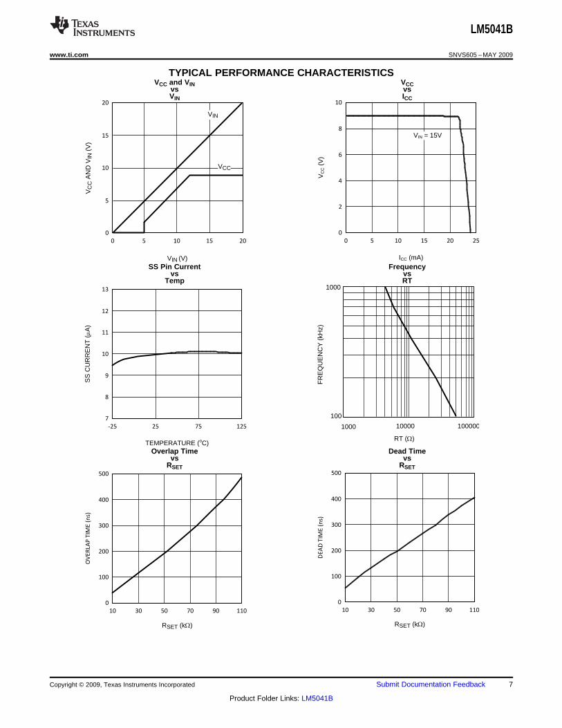
TYPICAL PERFORMANCE CHARACTERISTICSVCC and VIN VCC
vs vsVIN ICC
SS Pin Current Frequencyvs vs
Temp RT
Overlap Time Dead Timevs vs
RSET RSET
Copyright © 2009, Texas Instruments Incorporated Submit Documentation Feedback 7
Product Folder Links: LM5041B
-25 25 75 125
OV
ER
LAP
TIM
E (
ns)
TEMPERATURE (oC)
RSET = 20k:
120
110
100
90
80
70
60
-25 25 75 125
DE
AD
TIM
E (
ns)
TEMPERATURE (oC)
RSET = 20k:
130
120
110
100
90
80
70
LM5041B
SNVS605 –MAY 2009 www.ti.com
TYPICAL PERFORMANCE CHARACTERISTICS (continued)Overlap Time Dead Time
vs vsTemp Temp
Error Amplifier Gain Phase
8 Submit Documentation Feedback Copyright © 2009, Texas Instruments Incorporated
Product Folder Links: LM5041B
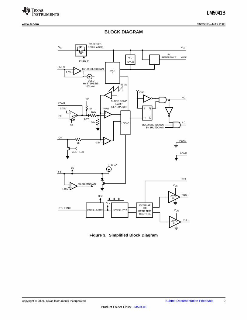
LOGIC
VIN VCC
VREF
SS
10 PA
RT / SYNC
LOGIC
PGND
AGND
5VREFERENCE
OSCILLATOR DIVIDE BY 2
PUSH
CLK
CLK
VCC
CS
TIME
OSC
45 PA
LD
FB
0.5V
PWM5k
5V
1.4V
100k
50k
CLK + LEB
COMP
0.75V
SS
R
S
Q
Q
HD
UVLO
UVLOHYSTERESIS
(20 PA)
2.5V
2k
SS
ENABLEVCC
UVLO
9V SERIESREGULATOR
+-
+-
c
+-
DRIVER
PULLDRIVER
SLOPE COMPRAMP
GENERATOR
VCC
OVERLAPOR
DEAD TIMECONTROL
+
-
UVLO SHUTDOWN
SS SHUTDOWN+-
0.45V
UVLO SHUTDOWNSS SHUTDOWN
LM5041B
www.ti.com SNVS605 –MAY 2009
BLOCK DIAGRAM
Figure 3. Simplified Block Diagram
Copyright © 2009, Texas Instruments Incorporated Submit Documentation Feedback 9
Product Folder Links: LM5041B
LM5041B
SNVS605 –MAY 2009 www.ti.com
DETAILED OPERATING DESCRIPTION
The LM5041B PWM controller contains all of the features necessary to implement either current-fed or voltage-fed push-pull or bridge power converters. These “Cascaded” topologies are well suited for multiple output andhigher power applications. The LM5041B includes these four control outputs: the buck stage controls (HD andLD) and the push-pull control outputs (PUSH and PULL). Push-pull outputs are driven at 50% nominal duty cycleat one half of the switching frequency of the buck stage and can be configured for either a specified overlap time(for current-fed applications) or a specified non-overlap time (for voltage-fed applications). Push-pull stageMOSFETs can be driven directly from the internal gate drivers while the buck stage requires an external driversuch as the LM5102. The LM5041B includes a high-voltage start-up regulator that operates over a wide inputrange of 15V to 100V. The PWM controller is designed for high-speed capability including an oscillator frequencyrange up to 1 MHz and total propagation delays of less than 100 ns. Additional features include line Under-Voltage Lock-Out (UVLO), Soft-Start, an error amplifier, precision voltage reference, and thermal shutdown.
High Voltage Start-Up Regulator
The LM5041B contains an internal high-voltage start-up regulator, thus the input pin (Vin) can be connecteddirectly to the line voltage. The regulator output is internally current limited to 15 mA. When power is applied, theregulator is enabled and sources current into an external capacitor connected to the Vcc pin. The recommendedcapacitance range for the Vcc regulator is 0.1µF to 100 µF. When the voltage on the Vcc pin reaches theregulation point of 9V, the internal voltage reference (REF) reaches its regulation point of 5V, and the soft-startcapacitor is charged above its shutdown threshold, the controller outputs are enabled. The Buck stage outputswill remain enabled until Vcc falls below 7V, the REF pin voltage falls below approximately 3V, the SS pin isforced below the 0.45V shutdown threshold or the line Under-Voltage Lock-Out detector indicates that Vin is outof range. The push-pull outputs continue switching until the REF pin voltage falls below approximately 3V. Intypical applications, an auxiliary transformer winding is connected through a diode to the Vcc pin. This windingmust raise the Vcc voltage above 9.3V to shut off the internal start-up regulator. Powering VCC from an auxiliarywinding improves efficiency while reducing the controller's power dissipation. The recommended capacitancerange for the Vref regulator output is 0.1µF to 10 µF.
The external VCC capacitor must be sized such that the capacitor maintains a VCC voltage greater than 7V duringthe initial start-up. During a fault mode when the converter auxiliary winding is inactive, external current draw onthe VCC line should be limited so the power dissipated in the start-up regulator does not exceed the maximumpower dissipation of the controller.
An external start-up or other bias rail can be used instead of the internal start-up regulator by connecting the VCCand the VIN pins together and feeding the external bias voltage into the two pins.
Line Under-Voltage Detector
The LM5041B contains a line Under-Voltage Lock-Out (UVLO) circuit. An external set-point resistor divider fromVIN to ground sets the operational range of the converter. The divider must be designed such that the voltage atthe UVLO pin will be greater than 2.5V when VIN is in the desired operating range. If the Under-Voltage thresholdis not met, both HD and LD will be forced to low state and VCC regulator will be disabled while the push-pulloutputs continue switching until the REF pin voltage falls below approximately 3V. ULVO hysteresis isaccomplished with an internal 20 µA current source that is switched on or off into the impedance of the set-pointdivider. When the UVLO threshold is exceeded, the current source is activated to instantly raise the voltage atthe UVLO pin. When the UVLO pin falls below the 2.5V threshold, the current source is turned off causing thevoltage at the UVLO pin to fall. The UVLO pin can also be used to implement a remote enable / disable function.By shorting the UVLO pin to ground, the converter can be disabled.
Buck Stage Control Outputs
The LM5041B Buck switch maximum duty cycle clamp ensures that there will be sufficient off time each cycle torecharge the bootstrap capacitor used in the high side gate driver. The Buck switch is specified to be off, and thesync switch on, for at least 250 ns per switching cycle. The Buck stage control outputs (LD and HD) are CMOSbuffers with logic levels of 0 to 5V.
During any fault state or Under-Voltage off state, both HD and LD state will be forced to low by the buck stagecontrol.
10 Submit Documentation Feedback Copyright © 2009, Texas Instruments Incorporated
Product Folder Links: LM5041B
K1 * RSET
PUSHDEADTIME
WAVEFORMS
PULL
PUSH
PULL
K1 * RSET
K2 * RSET
K2 * RSETOVERLAP
WAVEFORMS
LM5041B
www.ti.com SNVS605 –MAY 2009
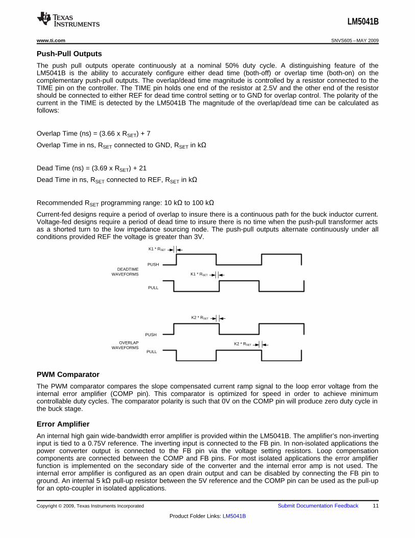
Push-Pull Outputs
The push pull outputs operate continuously at a nominal 50% duty cycle. A distinguishing feature of theLM5041B is the ability to accurately configure either dead time (both-off) or overlap time (both-on) on thecomplementary push-pull outputs. The overlap/dead time magnitude is controlled by a resistor connected to theTIME pin on the controller. The TIME pin holds one end of the resistor at 2.5V and the other end of the resistorshould be connected to either REF for dead time control setting or to GND for overlap control. The polarity of thecurrent in the TIME is detected by the LM5041B The magnitude of the overlap/dead time can be calculated asfollows:
Overlap Time (ns) = (3.66 x RSET) + 7
Overlap Time in ns, RSET connected to GND, RSET in kΩ
Dead Time (ns) = (3.69 x RSET) + 21
Dead Time in ns, RSET connected to REF, RSET in kΩ
Recommended RSET programming range: 10 kΩ to 100 kΩ
Current-fed designs require a period of overlap to insure there is a continuous path for the buck inductor current.Voltage-fed designs require a period of dead time to insure there is no time when the push-pull transformer actsas a shorted turn to the low impedance sourcing node. The push-pull outputs alternate continuously under allconditions provided REF the voltage is greater than 3V.
PWM Comparator
The PWM comparator compares the slope compensated current ramp signal to the loop error voltage from theinternal error amplifier (COMP pin). This comparator is optimized for speed in order to achieve minimumcontrollable duty cycles. The comparator polarity is such that 0V on the COMP pin will produce zero duty cycle inthe buck stage.
Error Amplifier
An internal high gain wide-bandwidth error amplifier is provided within the LM5041B. The amplifier’s non-invertinginput is tied to a 0.75V reference. The inverting input is connected to the FB pin. In non-isolated applications thepower converter output is connected to the FB pin via the voltage setting resistors. Loop compensationcomponents are connected between the COMP and FB pins. For most isolated applications the error amplifierfunction is implemented on the secondary side of the converter and the internal error amp is not used. Theinternal error amplifier is configured as an open drain output and can be disabled by connecting the FB pin toground. An internal 5 kΩ pull-up resistor between the 5V reference and the COMP pin can be used as the pull-upfor an opto-coupler in isolated applications.
Copyright © 2009, Texas Instruments Incorporated Submit Documentation Feedback 11
Product Folder Links: LM5041B
RT =(1/F) - 235 x 10-9
182 x 10-12 :
LM5041B
SNVS605 –MAY 2009 www.ti.com
Current Limit/Current Sense
The LM5041B provides cycle-by-cycle over-current protection. If the voltage at the CS comparator (CS pinvoltage plus slope comp voltage) exceeds 0.5V the present buck stage duty cycle is terminated (cycle by cyclecurrent limit). A small RC filter located near the controller is recommended to filter current sense signals at theCS pin. An internal MOSFET discharges the external CS pin for an additional 50 ns at the beginning of eachcycle to reduce the leading edge spike that occurs when the buck stage MOSFET is turned on.
The LM5041B current sense and PWM comparators are very fast, and may respond to short duration noisepulses. Layout considerations are critical for the current sense filter and sense resistor. The capacitor associatedwith the CS filter must be placed close to the device and connected directly to the pins of the controller (CS andGND). If a current sense transformer is used, both leads of the transformer secondary should be routed to thesense resistor, which should also be located close to the IC. A resistor may be used for current sensing insteadof a transformer, located in the push-pull transistor sources, but a low inductance type of resistor is required.When designing with a sense resistor, all of the noise sensitive low power grounds should be connected togetheraround the IC and a single connection should be made to the high current power ground (sense resistor groundpoint).
Oscillator and Sync Capability
The LM5041B oscillator is set by a single external resistor connected between the RT pin and GND. To set adesired oscillator frequency (F), the necessary RT resistor can be calculated from:
(1)
The buck stage will switch at the oscillator frequency and each push-pull output will switch at half the oscillatorfrequency in a push-pull configuration. The LM5041B can also be synchronized to an external clock. The externalclock must have a higher frequency than the free running frequency set by the RT resistor. The clock signalshould be capacitively coupled into the RT pin with a 100 pF capacitor. A peak voltage level greater than 3V isrequired for detection of the sync pulse. The sync pulse width should be set in the 15 ns to 150 ns range by theexternal components. The RT resistor is always required, whether the oscillator is free running or externallysynchronized. The voltage at the RT pin is internally regulated to 2V. The RT resistor should be located veryclose to the device and connected directly to the pins of the IC (RT and GND).
Slope Compensation
The PWM comparator compares the current sense signal to the voltage at the COMP pin. The output stage ofthe internal error amplifier generally drives the COMP pin. At duty cycles greater than 50%, current mode controlcircuits are subject to sub-harmonic oscillation. By adding an additional fixed ramp signal (slope compensation)to the current sense ramp, oscillations can be avoided. The LM5041B integrates this slope compensation bybuffering the internal oscillator ramp and summing a current ramp generated by the oscillator internally with thecurrent sense signal. Additional slope compensation may be provided by increasing the source impedance of thecurrent sense signal.
Soft-Start and Shutdown
The soft-start feature allows the power converter to gradually reach the initial steady state operating point,thereby reducing start-up stresses and surges. At power on, a 10 µA current is sourced out of the soft-start pin(SS) to charge an external capacitor. The capacitor voltage will ramp up slowly and will limit the maximum dutycycle of the buck stage. In the event of a fault as indicated by VCC Under-voltage, line Under-voltage the outputdrivers are disabled and the soft-start capacitor is discharged to 0.7V. When the fault condition is no longerpresent, a soft-start sequence will begin again and buck stage duty cycle will gradually increase as the soft-startcapacitor is charged.
The SS pin also serves as an enable input of HD and LD. Both HD and LD will be forced to a low state if the SSpin is below the shutdown threshold of 0.45V.
12 Submit Documentation Feedback Copyright © 2009, Texas Instruments Incorporated
Product Folder Links: LM5041B
LM5041B
www.ti.com SNVS605 –MAY 2009
Thermal Protection
Internal Thermal Shutdown circuitry is provided to protect the integrated circuit in the event that the maximumjunction temperature is exceeded. When activated, typically at 165 degrees Celsius, the controller is forced into alow-power standby state, disabling the output drivers and the bias regulator. This feature is provided to preventcatastrophic failures from accidental device overheating.
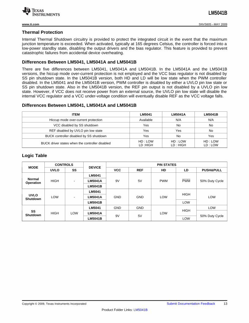
Differences Between LM5041, LM5041A and LM5041B
There are five differences between LM5041, LM5041A and LM5041B. In the LM5041A and the LM5041Bversions, the hiccup mode over-current protection is not employed and the VCC bias regulator is not disabled bySS pin shutdown state. In the LM5041B version, both HD and LD will be low state when the PWM controllerdisabled. In the LM5041 and the LM5041B version, PWM controller is disabled by either a UVLO pin low state orSS pin shutdown state. Also in the LM5041B version, the REF pin output is not disabled by a UVLO pin lowstate. However, if VCC does not receive power from an external source, the UVLO pin low state will disable theinternal VCC regulator and a VCC under-voltage condition will eventually disable REF as the VCC voltage falls.
Differences Between LM5041, LM5041A and LM5041B
ITEM LM5041 LM5041A LM5041B
Hiccup mode over-current protection Available N/A N/A
VCC disabled by SS shutdown Yes No No
REF disabled by UVLO pin low state Yes Yes No
BUCK controller disabled by SS shutdown Yes No Yes
HD : LOW HD : LOW HD : LOWBUCK driver states when the controller disabled LD :HIGH LD : HIGH LD : LOW
Logic Table
CONTROLS PIN STATESMODE DEVICE
UVLO SS VCC REF HD LD PUSH&PULL
LM5041Normal HIGH - LM5041A 9V 5V PWM PWM 50% Duty CycleOperation
LM5041B
LM5041HIGHUVLO LOW - LM5041A GND GND LOW LOWShutdown
LM5041B LOW
LM5041 GND GND LOWHIGHSS HIGH LOW LM5041A LOWShutdown 9V 5V 50% Duty Cycle
LM5041B LOW
Copyright © 2009, Texas Instruments Incorporated Submit Documentation Feedback 13
Product Folder Links: LM5041B
LM5102
PUSH
PULL
33V - 76V
HIVIN
LM5041B
VCC
HD
LD
COMP
VDD
HB
LO
VSS
RT1
LI
RT2
HO
HS
+
+
LM5100
HI
VDDHB
LO
LI
HO
HS
FEEDBACK
VOUT
L1
T1
T1
LM5041B
SNVS605 –MAY 2009 www.ti.com
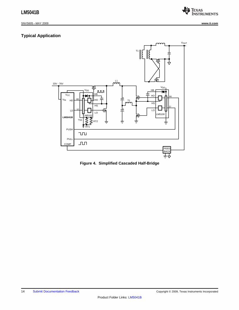
Typical Application
Figure 4. Simplified Cascaded Half-Bridge
14 Submit Documentation Feedback Copyright © 2009, Texas Instruments Incorporated
Product Folder Links: LM5041B
LM5041B
www.ti.com SNVS605 –MAY 2009
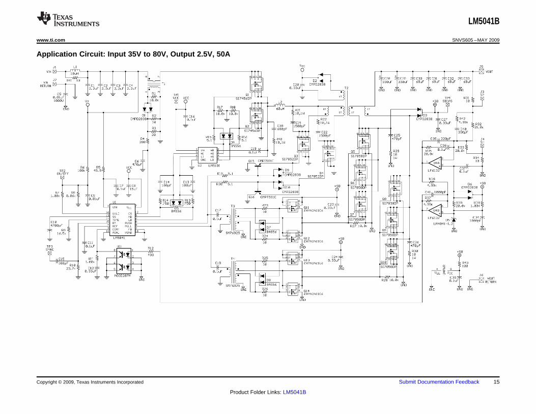
Application Circuit: Input 35V to 80V, Output 2.5V, 50A
Copyright © 2009, Texas Instruments Incorporated Submit Documentation Feedback 15
Product Folder Links: LM5041B
PACKAGE OPTION ADDENDUM
www.ti.com 11-Apr-2013
Addendum-Page 1
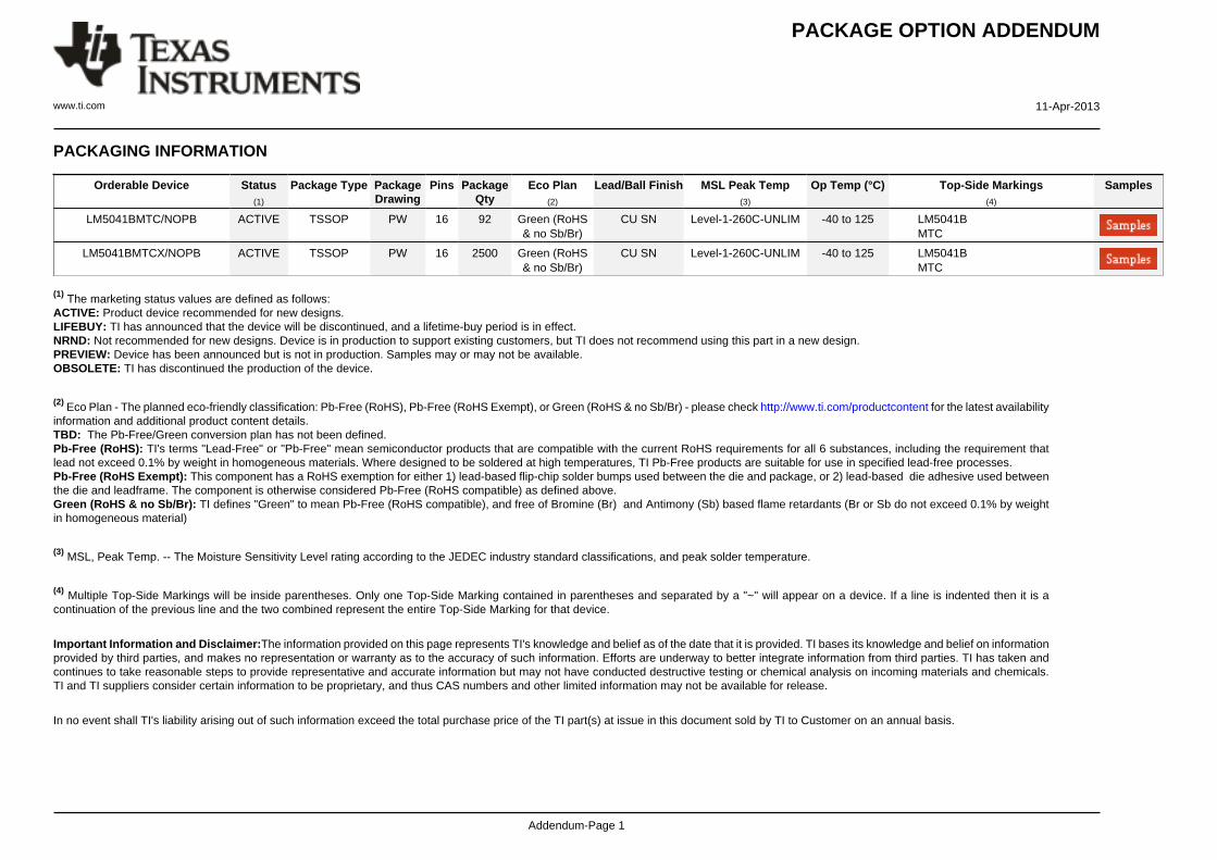
PACKAGING INFORMATION
Orderable Device Status(1)
Package Type PackageDrawing
Pins PackageQty
Eco Plan(2)
Lead/Ball Finish MSL Peak Temp(3)
Op Temp (°C) Top-Side Markings(4)
Samples
LM5041BMTC/NOPB ACTIVE TSSOP PW 16 92 Green (RoHS& no Sb/Br)
CU SN Level-1-260C-UNLIM -40 to 125 LM5041BMTC
LM5041BMTCX/NOPB ACTIVE TSSOP PW 16 2500 Green (RoHS& no Sb/Br)
CU SN Level-1-260C-UNLIM -40 to 125 LM5041BMTC
(1) The marketing status values are defined as follows:ACTIVE: Product device recommended for new designs.LIFEBUY: TI has announced that the device will be discontinued, and a lifetime-buy period is in effect.NRND: Not recommended for new designs. Device is in production to support existing customers, but TI does not recommend using this part in a new design.PREVIEW: Device has been announced but is not in production. Samples may or may not be available.OBSOLETE: TI has discontinued the production of the device.
(2) Eco Plan - The planned eco-friendly classification: Pb-Free (RoHS), Pb-Free (RoHS Exempt), or Green (RoHS & no Sb/Br) - please check http://www.ti.com/productcontent for the latest availabilityinformation and additional product content details.TBD: The Pb-Free/Green conversion plan has not been defined.Pb-Free (RoHS): TI's terms "Lead-Free" or "Pb-Free" mean semiconductor products that are compatible with the current RoHS requirements for all 6 substances, including the requirement thatlead not exceed 0.1% by weight in homogeneous materials. Where designed to be soldered at high temperatures, TI Pb-Free products are suitable for use in specified lead-free processes.Pb-Free (RoHS Exempt): This component has a RoHS exemption for either 1) lead-based flip-chip solder bumps used between the die and package, or 2) lead-based die adhesive used betweenthe die and leadframe. The component is otherwise considered Pb-Free (RoHS compatible) as defined above.Green (RoHS & no Sb/Br): TI defines "Green" to mean Pb-Free (RoHS compatible), and free of Bromine (Br) and Antimony (Sb) based flame retardants (Br or Sb do not exceed 0.1% by weightin homogeneous material)
(3) MSL, Peak Temp. -- The Moisture Sensitivity Level rating according to the JEDEC industry standard classifications, and peak solder temperature.
(4) Multiple Top-Side Markings will be inside parentheses. Only one Top-Side Marking contained in parentheses and separated by a "~" will appear on a device. If a line is indented then it is acontinuation of the previous line and the two combined represent the entire Top-Side Marking for that device.
Important Information and Disclaimer:The information provided on this page represents TI's knowledge and belief as of the date that it is provided. TI bases its knowledge and belief on informationprovided by third parties, and makes no representation or warranty as to the accuracy of such information. Efforts are underway to better integrate information from third parties. TI has taken andcontinues to take reasonable steps to provide representative and accurate information but may not have conducted destructive testing or chemical analysis on incoming materials and chemicals.TI and TI suppliers consider certain information to be proprietary, and thus CAS numbers and other limited information may not be available for release.
In no event shall TI's liability arising out of such information exceed the total purchase price of the TI part(s) at issue in this document sold by TI to Customer on an annual basis.
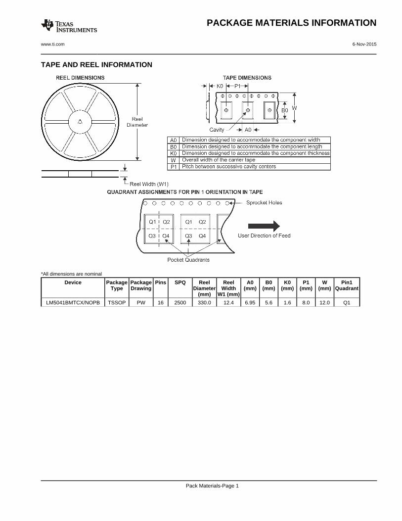
TAPE AND REEL INFORMATION
*All dimensions are nominal
Device PackageType
PackageDrawing
Pins SPQ ReelDiameter
(mm)
ReelWidth
W1 (mm)
A0(mm)
B0(mm)
K0(mm)
P1(mm)
W(mm)
Pin1Quadrant
LM5041BMTCX/NOPB TSSOP PW 16 2500 330.0 12.4 6.95 5.6 1.6 8.0 12.0 Q1
PACKAGE MATERIALS INFORMATION
www.ti.com 6-Nov-2015
Pack Materials-Page 1
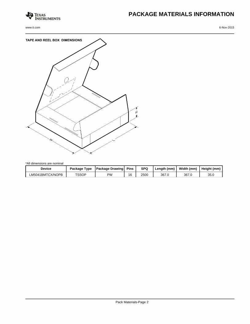
*All dimensions are nominal
Device Package Type Package Drawing Pins SPQ Length (mm) Width (mm) Height (mm)
LM5041BMTCX/NOPB TSSOP PW 16 2500 367.0 367.0 35.0
PACKAGE MATERIALS INFORMATION
www.ti.com 6-Nov-2015
Pack Materials-Page 2
IMPORTANT NOTICE
Texas Instruments Incorporated and its subsidiaries (TI) reserve the right to make corrections, enhancements, improvements and otherchanges to its semiconductor products and services per JESD46, latest issue, and to discontinue any product or service per JESD48, latestissue. Buyers should obtain the latest relevant information before placing orders and should verify that such information is current andcomplete. All semiconductor products (also referred to herein as “components”) are sold subject to TI’s terms and conditions of salesupplied at the time of order acknowledgment.TI warrants performance of its components to the specifications applicable at the time of sale, in accordance with the warranty in TI’s termsand conditions of sale of semiconductor products. Testing and other quality control techniques are used to the extent TI deems necessaryto support this warranty. Except where mandated by applicable law, testing of all parameters of each component is not necessarilyperformed.TI assumes no liability for applications assistance or the design of Buyers’ products. Buyers are responsible for their products andapplications using TI components. To minimize the risks associated with Buyers’ products and applications, Buyers should provideadequate design and operating safeguards.TI does not warrant or represent that any license, either express or implied, is granted under any patent right, copyright, mask work right, orother intellectual property right relating to any combination, machine, or process in which TI components or services are used. Informationpublished by TI regarding third-party products or services does not constitute a license to use such products or services or a warranty orendorsement thereof. Use of such information may require a license from a third party under the patents or other intellectual property of thethird party, or a license from TI under the patents or other intellectual property of TI.Reproduction of significant portions of TI information in TI data books or data sheets is permissible only if reproduction is without alterationand is accompanied by all associated warranties, conditions, limitations, and notices. TI is not responsible or liable for such altereddocumentation. Information of third parties may be subject to additional restrictions.Resale of TI components or services with statements different from or beyond the parameters stated by TI for that component or servicevoids all express and any implied warranties for the associated TI component or service and is an unfair and deceptive business practice.TI is not responsible or liable for any such statements.Buyer acknowledges and agrees that it is solely responsible for compliance with all legal, regulatory and safety-related requirementsconcerning its products, and any use of TI components in its applications, notwithstanding any applications-related information or supportthat may be provided by TI. Buyer represents and agrees that it has all the necessary expertise to create and implement safeguards whichanticipate dangerous consequences of failures, monitor failures and their consequences, lessen the likelihood of failures that might causeharm and take appropriate remedial actions. Buyer will fully indemnify TI and its representatives against any damages arising out of the useof any TI components in safety-critical applications.In some cases, TI components may be promoted specifically to facilitate safety-related applications. With such components, TI’s goal is tohelp enable customers to design and create their own end-product solutions that meet applicable functional safety standards andrequirements. Nonetheless, such components are subject to these terms.No TI components are authorized for use in FDA Class III (or similar life-critical medical equipment) unless authorized officers of the partieshave executed a special agreement specifically governing such use.Only those TI components which TI has specifically designated as military grade or “enhanced plastic” are designed and intended for use inmilitary/aerospace applications or environments. Buyer acknowledges and agrees that any military or aerospace use of TI componentswhich have not been so designated is solely at the Buyer's risk, and that Buyer is solely responsible for compliance with all legal andregulatory requirements in connection with such use.TI has specifically designated certain components as meeting ISO/TS16949 requirements, mainly for automotive use. In any case of use ofnon-designated products, TI will not be responsible for any failure to meet ISO/TS16949.
Products ApplicationsAudio www.ti.com/audio Automotive and Transportation www.ti.com/automotiveAmplifiers amplifier.ti.com Communications and Telecom www.ti.com/communicationsData Converters dataconverter.ti.com Computers and Peripherals www.ti.com/computersDLP® Products www.dlp.com Consumer Electronics www.ti.com/consumer-appsDSP dsp.ti.com Energy and Lighting www.ti.com/energyClocks and Timers www.ti.com/clocks Industrial www.ti.com/industrialInterface interface.ti.com Medical www.ti.com/medicalLogic logic.ti.com Security www.ti.com/securityPower Mgmt power.ti.com Space, Avionics and Defense www.ti.com/space-avionics-defenseMicrocontrollers microcontroller.ti.com Video and Imaging www.ti.com/videoRFID www.ti-rfid.comOMAP Applications Processors www.ti.com/omap TI E2E Community e2e.ti.comWireless Connectivity www.ti.com/wirelessconnectivity
Mailing Address: Texas Instruments, Post Office Box 655303, Dallas, Texas 75265Copyright © 2016, Texas Instruments Incorporated


![[shaderx7] 4.1 Practical Cascaded Shadow Maps](https://img.pdfslide.tips/doc/110x75/54b4d93f4a79593d368b46fc/shaderx7-41-practical-cascaded-shadow-maps.jpg)