Embed Size (px)
Citation preview
LMC6042
www.ti.com SNOS611E –AUGUST 1999–REVISED MARCH 2013
LMC6042 CMOS Dual Micropower Operational AmplifierCheck for Samples: LMC6042
1FEATURES DESCRIPTIONUltra-low power consumption and low input-leakage
2• Low Supply Current: 10 μA/Amp (typ)current are the hallmarks of the LMC6042. Providing
• Operates from 4.5V to 15V Single Supply input currents of only 2 fA typical, the LMC6042 can• Ultra Low Input Current: 2 fA (typ) operate from a single supply, has output swing
extending to each supply rail, and an input voltage• Rail-to-Rail Output Swingrange that includes ground.• Input Common-Mode Range Includes GroundThe LMC6042 is ideal for use in systems requiringultra-low power consumption. In addition, theAPPLICATIONSinsensitivity to latch-up, high output drive, and output
• Battery Monitoring and Power Conditioning swing to ground without requiring external pull-down• Photodiode and Infrared Detector Preamplifier resistors make it ideal for single-supply battery-
powered systems.• Silicon Based Transducer Systems• Hand-Held Analytic Instruments Other applications for the LMC6042 include bar code
reader amplifiers, magnetic and electric field• pH Probe Buffer Amplifierdetectors, and hand-held electrometers.
• Fire and Smoke Detection SystemsThis device is built with TI's advanced Double-Poly• Charge Amplifier for Piezoelectric TransducersSilicon-Gate CMOS process.
See the LMC6041 for a single, and the LMC6044 fora quad amplifier with these features.
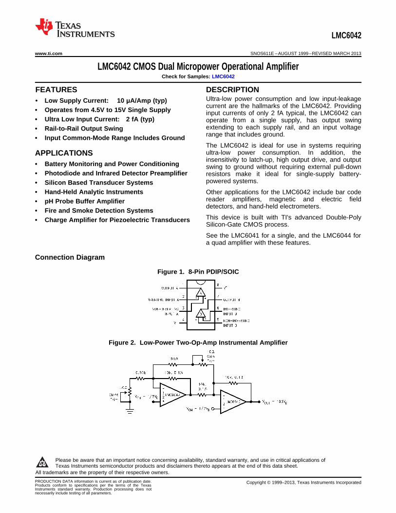
Connection Diagram
Figure 1. 8-Pin PDIP/SOIC
Figure 2. Low-Power Two-Op-Amp Instrumental Amplifier
1
Please be aware that an important notice concerning availability, standard warranty, and use in critical applications ofTexas Instruments semiconductor products and disclaimers thereto appears at the end of this data sheet.
2All trademarks are the property of their respective owners.
PRODUCTION DATA information is current as of publication date. Copyright © 1999–2013, Texas Instruments IncorporatedProducts conform to specifications per the terms of the TexasInstruments standard warranty. Production processing does notnecessarily include testing of all parameters.
LMC6042
SNOS611E –AUGUST 1999–REVISED MARCH 2013 www.ti.com
This integrated circuit can be damaged by ESD. Texas Instruments recommends that all integrated circuits be handled withappropriate precautions. Failure to observe proper handling and installation procedures can cause damage.
ESD damage can range from subtle performance degradation to complete device failure. Precision integrated circuits may be moresusceptible to damage because very small parametric changes could cause the device not to meet its published specifications.
Absolute Maximum Ratings (1) (2)
Differential Input Voltage ±Supply Voltage
Supply Voltage (V+ − V−) 16V
Output Short Circuit to V+ See (3)
Output Short Circuit to V− See (4)
Lead Temperature (Soldering, 10 seconds) 260°C
Current at Input Pin ±5 mA
Current at Output Pin ±18 mA
Current at Power Supply Pin 35 mA
Power Dissipation See (5)
Storage Temperature Range −65°C to +150°C
Junction Temperature (5) 110°C
ESD Tolerance (6) 500V
Voltage at Input/Output Pin (V+) + 0.3V, (V−) − 0.3V
(1) Absolute Maximum Ratings indicate limits beyond which damage to the device may occur. Operating Conditions indicate conditions forwhich the device is intended to be functional, but do not ensure specific performance limits. For ensured specifications and testconditions, see the Electrical Characteristics. The ensured specifications apply only for the test conditions listed.
(2) If Military/Aerospace specified devices are required, please contact the TI Sales Office/Distributors for availability and specifications.(3) Do not connect output to V+when V+ is greater than 13V or reliability may be adversely affected.(4) Applies to both single-supply operation. Continuous short circuit operation at elevated ambient temperature can result in exceeding the
maximum allowed junction temperature of 110°C. Output currents in excess of ±30 mA over long term may adversely affect reliability.(5) The maximum power dissipation is a function of TJ(Max), θJA, and TA. The maximum allowable power dissipation at any ambient
temperature is PD = (TJ(Max) − TA)/θJA.(6) Human body model, 1.5 kΩ in series with 100 pF.
Operating RatingsTemperature Range LMC6042AI, LMC6042I −40°C ≤ TJ ≤ +85°C
Supply Voltage 4.5V ≤ V+ ≤ 15.5V
Power Dissipation See (1)
Thermal Resistance (θJA), (2) 8-Pin PDIP 101°C/W
8-Pin SOIC 165°C/W
8-Pin CDIP 115°C/W
(1) For operating at elevated temperatures the device must be derated based on the thermal resistance θJA with PD = (TJ − TA)/θJA.(2) All numbers apply for packages soldered directly into a PC board.
Electrical CharacteristicsUnless otherwise specified, all limits ensured for TA = TJ = 25°C. Boldface limits apply at the temperature extremes. V+ = 5V,V− = 0V, VCM = 1.5V, VO = V+/2 and RL > 1M unless otherwise specified.
Typical (1) LMC6042AI LMC6042I UnitsSymbol Parameter Conditions (Limit)Limit (2) Limit (2)
VOS Input Offset Voltage 1 3 6 mV
3.3 6.3 Max
TCVOS Input Offset Voltage 1.3 μV/°C
Average Drift
IB Input Bias Current 0.002 4 4 pA (Max)
IOS Input Offset Current 0.001 2 2 pA (Max)
RIN Input Resistance >10 TeraΩ
(1) Typical values represent the most likely parametric norm.(2) All limits are specified at room temperature (standard type face) or at operating temperature extremes (bold face type).
2 Submit Documentation Feedback Copyright © 1999–2013, Texas Instruments Incorporated
Product Folder Links: LMC6042
LMC6042
www.ti.com SNOS611E –AUGUST 1999–REVISED MARCH 2013
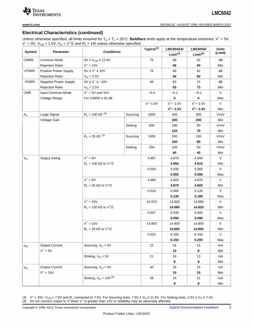
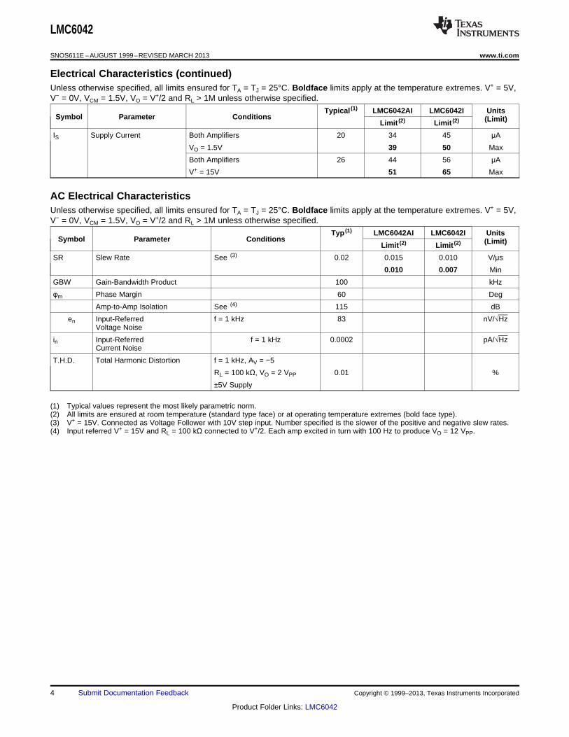
Electrical Characteristics (continued)Unless otherwise specified, all limits ensured for TA = TJ = 25°C. Boldface limits apply at the temperature extremes. V+ = 5V,V− = 0V, VCM = 1.5V, VO = V+/2 and RL > 1M unless otherwise specified.
Typical (1) LMC6042AI LMC6042I UnitsSymbol Parameter Conditions (Limit)Limit (2) Limit (2)
CMRR Common Mode 0V ≤ VCM ≤ 12.0V 75 68 62 dB
Rejection Ratio V+ = 15V 66 60 Min
+PSRR Positive Power Supply 5V ≤ V+ ≤ 15V 75 68 62 dB
Rejection Ratio VO = 2.5V 66 60 Min
−PSRR Negative Power Supply 0V ≤ V− ≤ −10V 94 84 74 dB
Rejection Ratio VO = 2.5V 83 73 Min
CMR Input Common-Mode V+ = 5V and 15V −0.4 −0.1 −0.1 V
Voltage Range For CMRR ≥ 50 dB 0 0 Max
V+−1.9V V+− 2.3V V+− 2.3V V
V+− 2.5V V+− 2.4V Min
AV Large Signal RL = 100 kΩ (3) Sourcing 1000 400 300 V/mV
Voltage Gain 300 200 Min
Sinking 500 180 90 V/mV
120 70 Min
RL = 25 kΩ (3) Sourcing 1000 200 100 V/mV
160 80 Min
Sinking 250 100 50 V/mV
60 40 Min
VO Output Swing V+ = 5V 4.987 4.970 4.940 V
RL = 100 kΩ to V+/2 4.950 4.910 Min
0.004 0.030 0.060 V
0.050 0.090 Max
V+ = 5V 4.980 4.920 4.870 V
RL = 25 kΩ to V+/2 4.870 4.820 Min
0.010 0.080 0.130 V
0.130 0.180 Max
V+ = 15V 14.970 14.920 14.880 V
RL = 100 kΩ to V+/2 14.880 14.820 Min
0.007 0.030 0.060 V
0.050 0.090 Max
V+ = 15V 14.950 14.900 14.850 V
RL = 25 kΩ to V+/2 14.850 14.800 Min
0.022 0.100 0.150 V
0.150 0.200 Max
ISC Output Current Sourcing, VO = 0V 22 16 13 mA
V+ = 5V 10 8 Min
Sinking, VO = 5V 21 16 13 mA
8 8 Min
ISC Output Current Sourcing, VO = 0V 40 15 15 mA
V+ = 15V 10 10 Min
Sinking, VO = 13V (4) 39 24 21 mA
8 8 Min
(3) V+ = 15V, VCM = 7.5V and RL connected to 7.5V. For Sourcing tests, 7.5V ≤ VO ≤ 11.5V. For Sinking tests, 2.5V ≤ VO ≤ 7.5V.(4) Do not connect output to V+when V+ is greater than 13V or reliability may be adversely affected.
Copyright © 1999–2013, Texas Instruments Incorporated Submit Documentation Feedback 3
Product Folder Links: LMC6042
LMC6042
SNOS611E –AUGUST 1999–REVISED MARCH 2013 www.ti.com
Electrical Characteristics (continued)Unless otherwise specified, all limits ensured for TA = TJ = 25°C. Boldface limits apply at the temperature extremes. V+ = 5V,V− = 0V, VCM = 1.5V, VO = V+/2 and RL > 1M unless otherwise specified.
Typical (1) LMC6042AI LMC6042I UnitsSymbol Parameter Conditions (Limit)Limit (2) Limit (2)
IS Supply Current Both Amplifiers 20 34 45 μA
VO = 1.5V 39 50 Max
Both Amplifiers 26 44 56 μA
V+ = 15V 51 65 Max
AC Electrical CharacteristicsUnless otherwise specified, all limits ensured for TA = TJ = 25°C. Boldface limits apply at the temperature extremes. V+ = 5V,V− = 0V, VCM = 1.5V, VO = V+/2 and RL > 1M unless otherwise specified.
Typ (1) LMC6042AI LMC6042I UnitsSymbol Parameter Conditions (Limit)Limit (2) Limit (2)
SR Slew Rate See (3) 0.02 0.015 0.010 V/μs
0.010 0.007 Min
GBW Gain-Bandwidth Product 100 kHz
φm Phase Margin 60 Deg
Amp-to-Amp Isolation See (4) 115 dB
en Input-Referred f = 1 kHz 83 nV/√HzVoltage Noise
in Input-Referred f = 1 kHz 0.0002 pA/√HzCurrent Noise
T.H.D. Total Harmonic Distortion f = 1 kHz, AV = −5
RL = 100 kΩ, VO = 2 VPP 0.01 %
±5V Supply
(1) Typical values represent the most likely parametric norm.(2) All limits are ensured at room temperature (standard type face) or at operating temperature extremes (bold face type).(3) V+ = 15V. Connected as Voltage Follower with 10V step input. Number specified is the slower of the positive and negative slew rates.(4) Input referred V+ = 15V and RL = 100 kΩ connected to V+/2. Each amp excited in turn with 100 Hz to produce VO = 12 VPP.
4 Submit Documentation Feedback Copyright © 1999–2013, Texas Instruments Incorporated
Product Folder Links: LMC6042
LMC6042
www.ti.com SNOS611E –AUGUST 1999–REVISED MARCH 2013
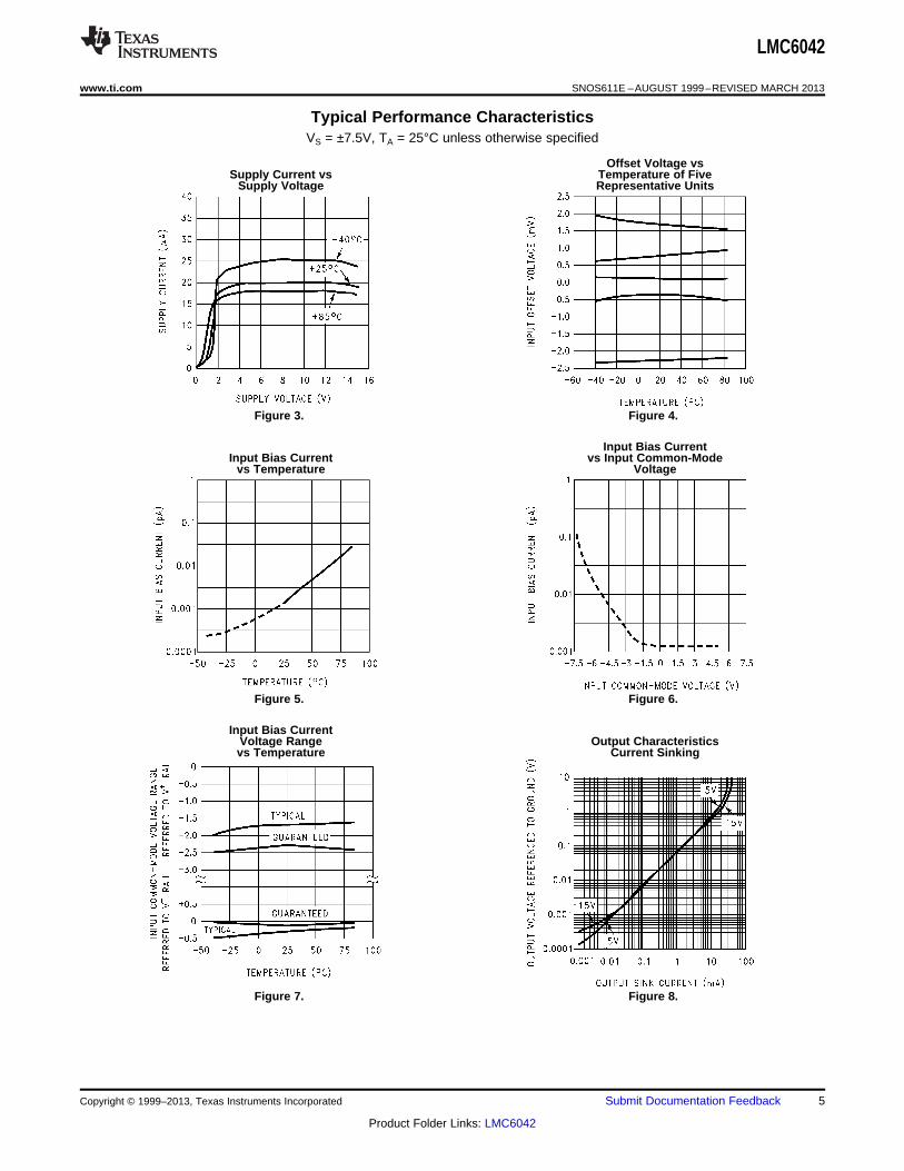
Typical Performance CharacteristicsVS = ±7.5V, TA = 25°C unless otherwise specified
Offset Voltage vsSupply Current vs Temperature of Five
Supply Voltage Representative Units
Figure 3. Figure 4.
Input Bias CurrentInput Bias Current vs Input Common-Mode
vs Temperature Voltage
Figure 5. Figure 6.
Input Bias CurrentVoltage Range Output Characteristicsvs Temperature Current Sinking
Figure 7. Figure 8.
Copyright © 1999–2013, Texas Instruments Incorporated Submit Documentation Feedback 5
Product Folder Links: LMC6042
LMC6042
SNOS611E –AUGUST 1999–REVISED MARCH 2013 www.ti.com
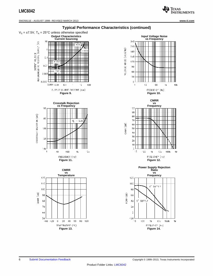
Typical Performance Characteristics (continued)VS = ±7.5V, TA = 25°C unless otherwise specified
Output Characteristics Input Voltage NoiseCurrent Sourcing vs Frequency
Figure 9. Figure 10.
CMRRCrosstalk Rejection vs
vs Frequency Frequency
Figure 11. Figure 12.
Power Supply RejectionCMRR Ratio
vs vsTemperature Frequency
Figure 13. Figure 14.
6 Submit Documentation Feedback Copyright © 1999–2013, Texas Instruments Incorporated
Product Folder Links: LMC6042
LMC6042
www.ti.com SNOS611E –AUGUST 1999–REVISED MARCH 2013
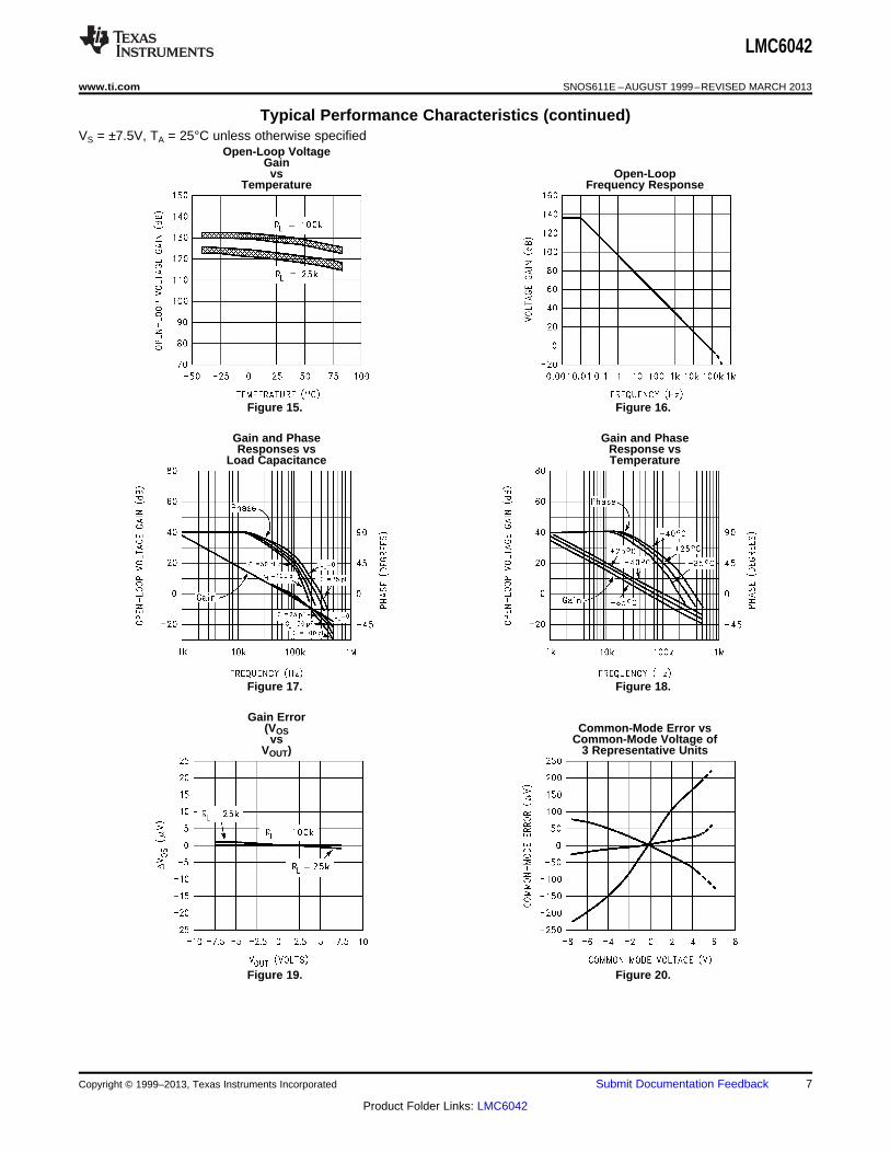
Typical Performance Characteristics (continued)VS = ±7.5V, TA = 25°C unless otherwise specified
Open-Loop VoltageGainvs Open-Loop
Temperature Frequency Response
Figure 15. Figure 16.
Gain and Phase Gain and PhaseResponses vs Response vs
Load Capacitance Temperature
Figure 17. Figure 18.
Gain Error(VOS Common-Mode Error vsvs Common-Mode Voltage of
VOUT) 3 Representative Units
Figure 19. Figure 20.
Copyright © 1999–2013, Texas Instruments Incorporated Submit Documentation Feedback 7
Product Folder Links: LMC6042
LMC6042
SNOS611E –AUGUST 1999–REVISED MARCH 2013 www.ti.com
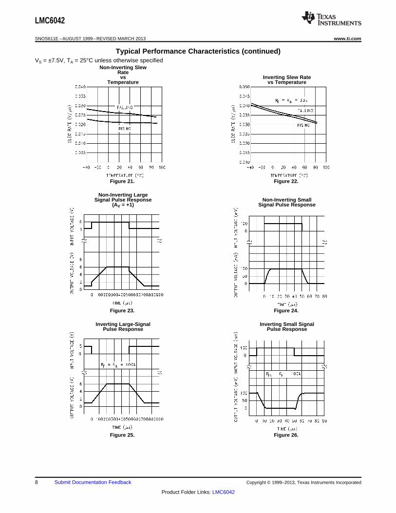
Typical Performance Characteristics (continued)VS = ±7.5V, TA = 25°C unless otherwise specified
Non-Inverting SlewRatevs Inverting Slew Rate
Temperature vs Temperature
Figure 21. Figure 22.
Non-Inverting LargeSignal Pulse Response Non-Inverting Small
(AV = +1) Signal Pulse Response
Figure 23. Figure 24.
Inverting Large-Signal Inverting Small SignalPulse Response Pulse Response
Figure 25. Figure 26.
8 Submit Documentation Feedback Copyright © 1999–2013, Texas Instruments Incorporated
Product Folder Links: LMC6042
LMC6042
www.ti.com SNOS611E –AUGUST 1999–REVISED MARCH 2013
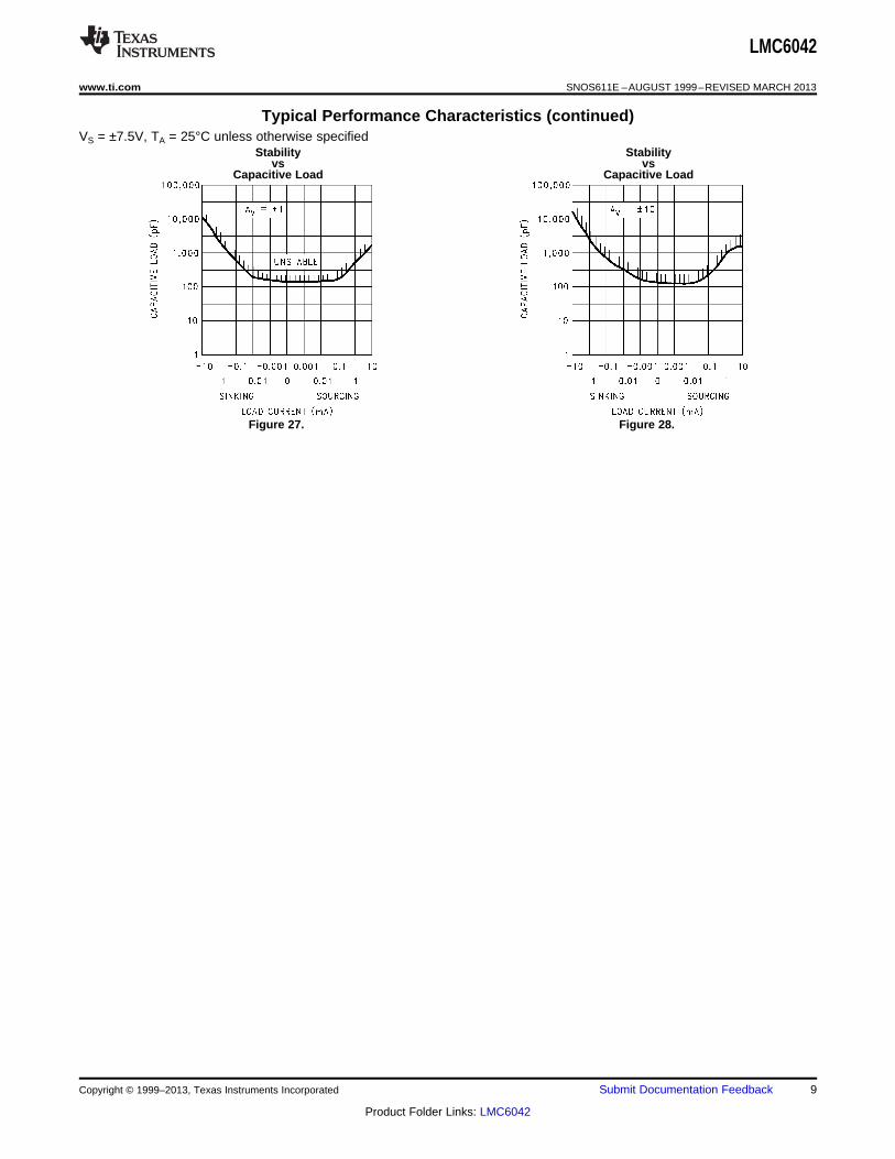
Typical Performance Characteristics (continued)VS = ±7.5V, TA = 25°C unless otherwise specified
Stability Stabilityvs vs
Capacitive Load Capacitive Load
Figure 27. Figure 28.
Copyright © 1999–2013, Texas Instruments Incorporated Submit Documentation Feedback 9
Product Folder Links: LMC6042
LMC6042
SNOS611E –AUGUST 1999–REVISED MARCH 2013 www.ti.com
APPLICATIONS HINTS
AMPLIFIER TOPOLOGY
The LMC6042 incorporates a novel op-amp design topology that enables it to maintain rail-to-rail output swingeven when driving a large load. Instead of relying on a push-pull unity gain output buffer stage, the output stageis taken directly from the internal integrator, which provides both low output impedance and large gain. Specialfeed-forward compensation design techniques are incorporated to maintain stability over a wider range ofoperating conditions than traditional micropower op-amps. These features make the LMC6042 both easier todesign with, and provide higher speed than products typically found in this ultra-low power class.
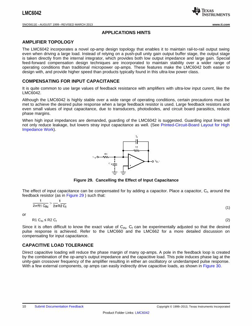
COMPENSATING FOR INPUT CAPACITANCE
It is quite common to use large values of feedback resistance with amplifiers with ultra-low input curent, like theLMC6042.
Although the LMC6042 is highly stable over a wide range of operating conditions, certain precautions must bemet to achieve the desired pulse response when a large feedback resistor is used. Large feedback resistors andeven small values of input capacitance, due to transducers, photodiodes, and circuit board parasitics, reducephase margins.
When high input impedances are demanded, guarding of the LMC6042 is suggested. Guarding input lines willnot only reduce leakage, but lowers stray input capacitance as well. (See Printed-Circuit-Board Layout for HighImpedance Work).
Figure 29. Cancelling the Effect of Input Capacitance
The effect of input capacitance can be compensated for by adding a capacitor. Place a capacitor, Cf, around thefeedback resistor (as in Figure 29 ) such that:
(1)
orR1 CIN ≤ R2 Cf (2)
Since it is often difficult to know the exact value of CIN, Cf can be experimentally adjusted so that the desiredpulse response is achieved. Refer to the LMC660 and the LMC662 for a more detailed discussion oncompensating for input capacitance.
CAPACITIVE LOAD TOLERANCE
Direct capacitive loading will reduce the phase margin of many op-amps. A pole in the feedback loop is createdby the combination of the op-amp's output impedance and the capacitive load. This pole induces phase lag at theunity-gain crossover frequency of the amplifier resulting in either an oscillatory or underdamped pulse response.With a few external components, op amps can easily indirectly drive capacitive loads, as shown in Figure 30.
10 Submit Documentation Feedback Copyright © 1999–2013, Texas Instruments Incorporated
Product Folder Links: LMC6042
LMC6042
www.ti.com SNOS611E –AUGUST 1999–REVISED MARCH 2013
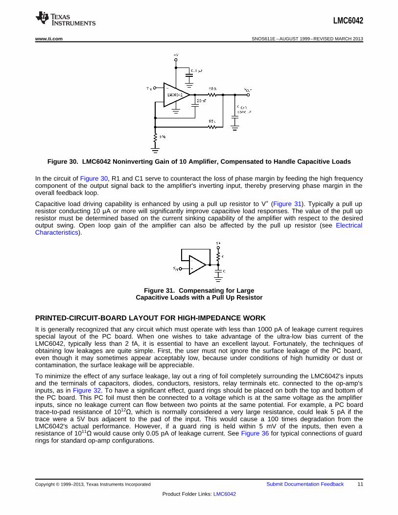
Figure 30. LMC6042 Noninverting Gain of 10 Amplifier, Compensated to Handle Capacitive Loads
In the circuit of Figure 30, R1 and C1 serve to counteract the loss of phase margin by feeding the high frequencycomponent of the output signal back to the amplifier's inverting input, thereby preserving phase margin in theoverall feedback loop.
Capacitive load driving capability is enhanced by using a pull up resistor to V+ (Figure 31). Typically a pull upresistor conducting 10 μA or more will significantly improve capacitive load responses. The value of the pull upresistor must be determined based on the current sinking capability of the amplifier with respect to the desiredoutput swing. Open loop gain of the amplifier can also be affected by the pull up resistor (see ElectricalCharacteristics).
Figure 31. Compensating for LargeCapacitive Loads with a Pull Up Resistor
PRINTED-CIRCUIT-BOARD LAYOUT FOR HIGH-IMPEDANCE WORK
It is generally recognized that any circuit which must operate with less than 1000 pA of leakage current requiresspecial layout of the PC board. When one wishes to take advantage of the ultra-low bias current of theLMC6042, typically less than 2 fA, it is essential to have an excellent layout. Fortunately, the techniques ofobtaining low leakages are quite simple. First, the user must not ignore the surface leakage of the PC board,even though it may sometimes appear acceptably low, because under conditions of high humidity or dust orcontamination, the surface leakage will be appreciable.
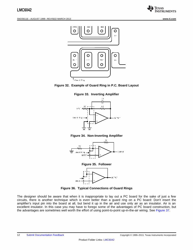
To minimize the effect of any surface leakage, lay out a ring of foil completely surrounding the LMC6042's inputsand the terminals of capacitors, diodes, conductors, resistors, relay terminals etc. connected to the op-amp'sinputs, as in Figure 32. To have a significant effect, guard rings should be placed on both the top and bottom ofthe PC board. This PC foil must then be connected to a voltage which is at the same voltage as the amplifierinputs, since no leakage current can flow between two points at the same potential. For example, a PC boardtrace-to-pad resistance of 1012Ω, which is normally considered a very large resistance, could leak 5 pA if thetrace were a 5V bus adjacent to the pad of the input. This would cause a 100 times degradation from theLMC6042's actual performance. However, if a guard ring is held within 5 mV of the inputs, then even aresistance of 1011Ω would cause only 0.05 pA of leakage current. See Figure 36 for typical connections of guardrings for standard op-amp configurations.
Copyright © 1999–2013, Texas Instruments Incorporated Submit Documentation Feedback 11
Product Folder Links: LMC6042
LMC6042
SNOS611E –AUGUST 1999–REVISED MARCH 2013 www.ti.com
Figure 32. Example of Guard Ring in P.C. Board Layout
Figure 33. Inverting Amplifier
Figure 34. Non-Inverting Amplifier
Figure 35. Follower
Figure 36. Typical Connections of Guard Rings
The designer should be aware that when it is inappropriate to lay out a PC board for the sake of just a fewcircuits, there is another technique which is even better than a guard ring on a PC board: Don't insert theamplifier's input pin into the board at all, but bend it up in the air and use only air as an insulator. Air is anexcellent insulator. In this case you may have to forego some of the advantages of PC board construction, butthe advantages are sometimes well worth the effort of using point-to-point up-in-the-air wiring. See Figure 37.
12 Submit Documentation Feedback Copyright © 1999–2013, Texas Instruments Incorporated
Product Folder Links: LMC6042
LMC6042
www.ti.com SNOS611E –AUGUST 1999–REVISED MARCH 2013
(Input pins are lifted out of PC board and soldered directly to components. All other pins connected to PC board.)
Figure 37. Air Wiring
Typical Single-Supply Applications
(V+ = 5.0 VDC)
The extremely high input impedance, and low power consumption, of the LMC6042 make it ideal for applicationsthat require battery-powered instrumentation amplifiers. Examples of these types of applications are hand-heldpH probes, analytic medical instruments, magnetic field detectors, gas detectors, and silicon based pressuretransducers.
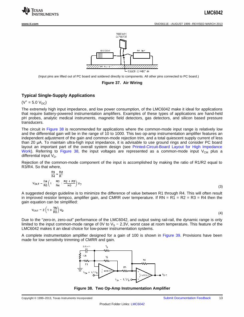
The circuit in Figure 38 is recommended for applications where the common-mode input range is relatively lowand the differential gain will be in the range of 10 to 1000. This two op-amp instrumentation amplifier features anindependent adjustment of the gain and common-mode rejection trim, and a total quiescent supply current of lessthan 20 μA. To maintain ultra-high input impedance, it is advisable to use ground rings and consider PC boardlayout an important part of the overall system design (see Printed-Circuit-Board Layout for High ImpedanceWork). Referring to Figure 38, the input voltages are represented as a common-mode input VCM plus adifferential input VD.
Rejection of the common-mode component of the input is accomplished by making the ratio of R1/R2 equal toR3/R4. So that where,
(3)
A suggested design guideline is to minimize the difference of value between R1 through R4. This will often resultin improved resistor tempco, amplifier gain, and CMRR over temperature. If RN = R1 = R2 = R3 = R4 then thegain equation can be simplified:
(4)
Due to the “zero-in, zero-out” performance of the LMC6042, and output swing rail-rail, the dynamic range is onlylimited to the input common-mode range of 0V to VS − 2.3V, worst case at room temperature. This feature of theLMC6042 makes it an ideal choice for low-power instrumentation systems.
A complete instrumentation amplifier designed for a gain of 100 is shown in Figure 39. Provisions have beenmade for low sensitivity trimming of CMRR and gain.
Figure 38. Two Op-Amp Instrumentation Amplifier
Copyright © 1999–2013, Texas Instruments Incorporated Submit Documentation Feedback 13
Product Folder Links: LMC6042
LMC6042
SNOS611E –AUGUST 1999–REVISED MARCH 2013 www.ti.com
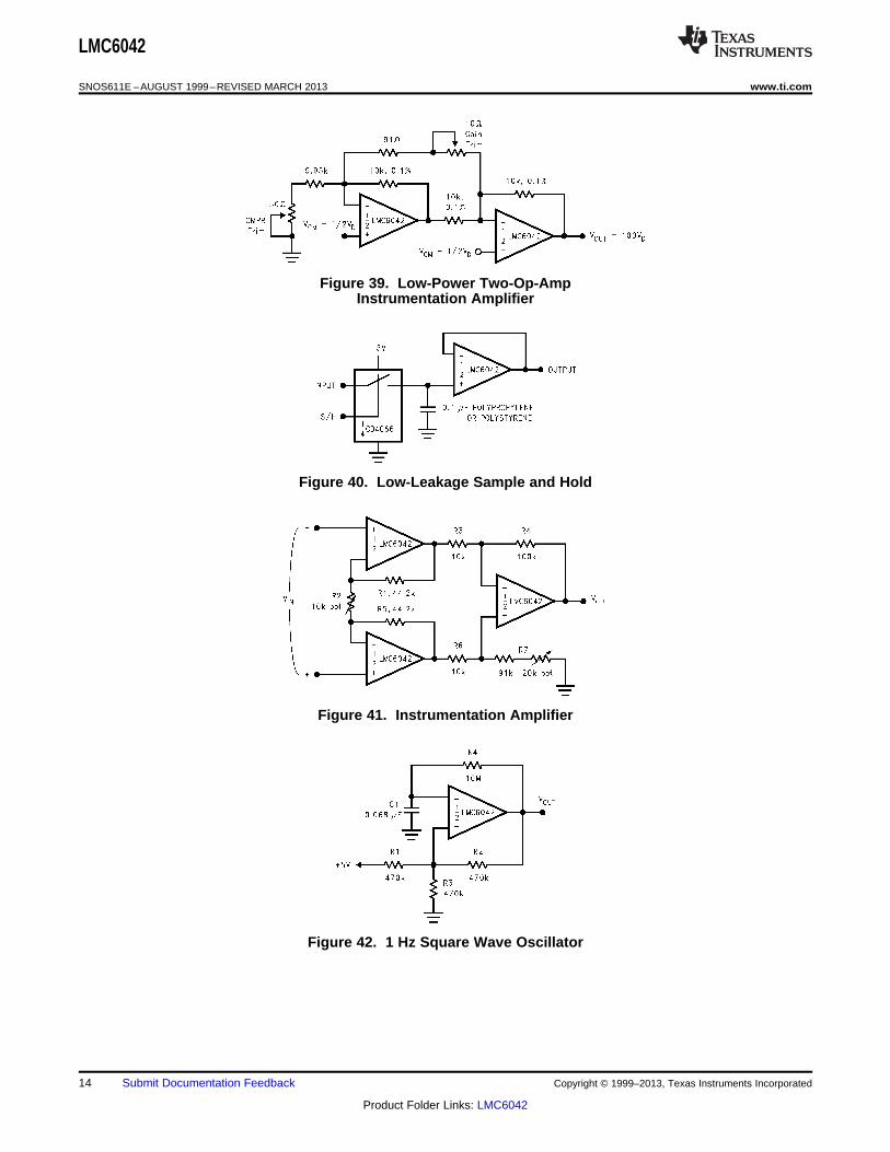
Figure 39. Low-Power Two-Op-AmpInstrumentation Amplifier
Figure 40. Low-Leakage Sample and Hold
Figure 41. Instrumentation Amplifier
Figure 42. 1 Hz Square Wave Oscillator
14 Submit Documentation Feedback Copyright © 1999–2013, Texas Instruments Incorporated
Product Folder Links: LMC6042
LMC6042
www.ti.com SNOS611E –AUGUST 1999–REVISED MARCH 2013
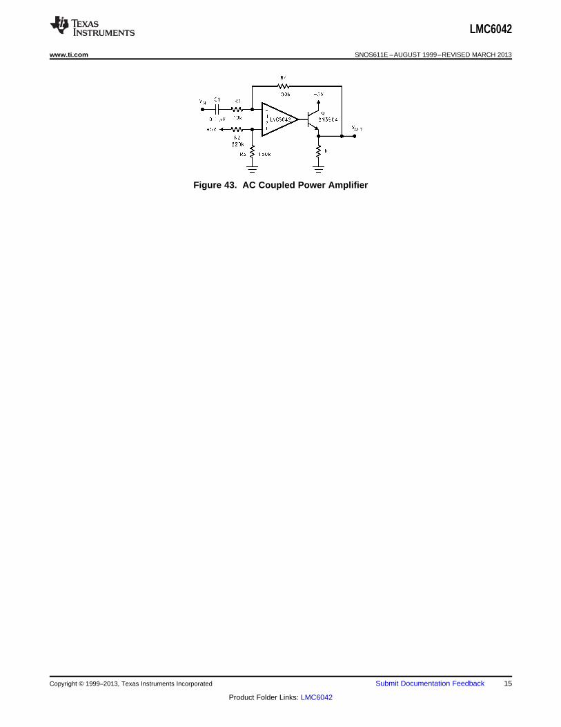
Figure 43. AC Coupled Power Amplifier
Copyright © 1999–2013, Texas Instruments Incorporated Submit Documentation Feedback 15
Product Folder Links: LMC6042
LMC6042
SNOS611E –AUGUST 1999–REVISED MARCH 2013 www.ti.com
REVISION HISTORY
Changes from Revision D (March 2013) to Revision E Page
• Changed layout of National Data Sheet to TI format .......................................................................................................... 15
16 Submit Documentation Feedback Copyright © 1999–2013, Texas Instruments Incorporated
Product Folder Links: LMC6042
PACKAGE OPTION ADDENDUM
www.ti.com 17-Mar-2017
Addendum-Page 1
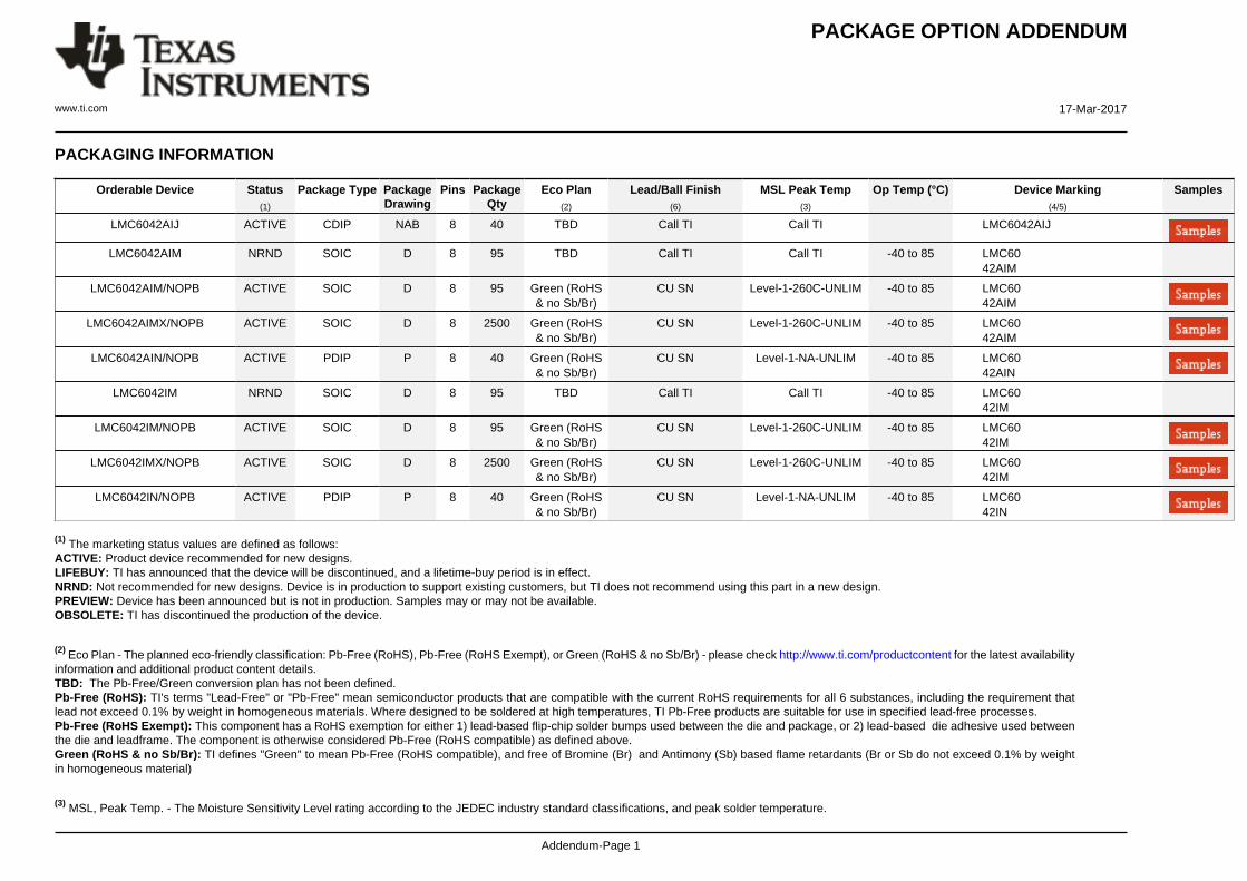
PACKAGING INFORMATION
Orderable Device Status(1)
Package Type PackageDrawing
Pins PackageQty
Eco Plan(2)
Lead/Ball Finish(6)
MSL Peak Temp(3)
Op Temp (°C) Device Marking(4/5)
Samples
LMC6042AIJ ACTIVE CDIP NAB 8 40 TBD Call TI Call TI LMC6042AIJ
LMC6042AIM NRND SOIC D 8 95 TBD Call TI Call TI -40 to 85 LMC6042AIM
LMC6042AIM/NOPB ACTIVE SOIC D 8 95 Green (RoHS& no Sb/Br)
CU SN Level-1-260C-UNLIM -40 to 85 LMC6042AIM
LMC6042AIMX/NOPB ACTIVE SOIC D 8 2500 Green (RoHS& no Sb/Br)
CU SN Level-1-260C-UNLIM -40 to 85 LMC6042AIM
LMC6042AIN/NOPB ACTIVE PDIP P 8 40 Green (RoHS& no Sb/Br)
CU SN Level-1-NA-UNLIM -40 to 85 LMC6042AIN
LMC6042IM NRND SOIC D 8 95 TBD Call TI Call TI -40 to 85 LMC6042IM
LMC6042IM/NOPB ACTIVE SOIC D 8 95 Green (RoHS& no Sb/Br)
CU SN Level-1-260C-UNLIM -40 to 85 LMC6042IM
LMC6042IMX/NOPB ACTIVE SOIC D 8 2500 Green (RoHS& no Sb/Br)
CU SN Level-1-260C-UNLIM -40 to 85 LMC6042IM
LMC6042IN/NOPB ACTIVE PDIP P 8 40 Green (RoHS& no Sb/Br)
CU SN Level-1-NA-UNLIM -40 to 85 LMC6042IN
(1) The marketing status values are defined as follows:ACTIVE: Product device recommended for new designs.LIFEBUY: TI has announced that the device will be discontinued, and a lifetime-buy period is in effect.NRND: Not recommended for new designs. Device is in production to support existing customers, but TI does not recommend using this part in a new design.PREVIEW: Device has been announced but is not in production. Samples may or may not be available.OBSOLETE: TI has discontinued the production of the device.
(2) Eco Plan - The planned eco-friendly classification: Pb-Free (RoHS), Pb-Free (RoHS Exempt), or Green (RoHS & no Sb/Br) - please check http://www.ti.com/productcontent for the latest availabilityinformation and additional product content details.TBD: The Pb-Free/Green conversion plan has not been defined.Pb-Free (RoHS): TI's terms "Lead-Free" or "Pb-Free" mean semiconductor products that are compatible with the current RoHS requirements for all 6 substances, including the requirement thatlead not exceed 0.1% by weight in homogeneous materials. Where designed to be soldered at high temperatures, TI Pb-Free products are suitable for use in specified lead-free processes.Pb-Free (RoHS Exempt): This component has a RoHS exemption for either 1) lead-based flip-chip solder bumps used between the die and package, or 2) lead-based die adhesive used betweenthe die and leadframe. The component is otherwise considered Pb-Free (RoHS compatible) as defined above.Green (RoHS & no Sb/Br): TI defines "Green" to mean Pb-Free (RoHS compatible), and free of Bromine (Br) and Antimony (Sb) based flame retardants (Br or Sb do not exceed 0.1% by weightin homogeneous material)
(3) MSL, Peak Temp. - The Moisture Sensitivity Level rating according to the JEDEC industry standard classifications, and peak solder temperature.
PACKAGE OPTION ADDENDUM
www.ti.com 17-Mar-2017
Addendum-Page 2
(4) There may be additional marking, which relates to the logo, the lot trace code information, or the environmental category on the device.
(5) Multiple Device Markings will be inside parentheses. Only one Device Marking contained in parentheses and separated by a "~" will appear on a device. If a line is indented then it is a continuationof the previous line and the two combined represent the entire Device Marking for that device.
(6) Lead/Ball Finish - Orderable Devices may have multiple material finish options. Finish options are separated by a vertical ruled line. Lead/Ball Finish values may wrap to two lines if the finishvalue exceeds the maximum column width.
Important Information and Disclaimer:The information provided on this page represents TI's knowledge and belief as of the date that it is provided. TI bases its knowledge and belief on informationprovided by third parties, and makes no representation or warranty as to the accuracy of such information. Efforts are underway to better integrate information from third parties. TI has taken andcontinues to take reasonable steps to provide representative and accurate information but may not have conducted destructive testing or chemical analysis on incoming materials and chemicals.TI and TI suppliers consider certain information to be proprietary, and thus CAS numbers and other limited information may not be available for release.
In no event shall TI's liability arising out of such information exceed the total purchase price of the TI part(s) at issue in this document sold by TI to Customer on an annual basis.
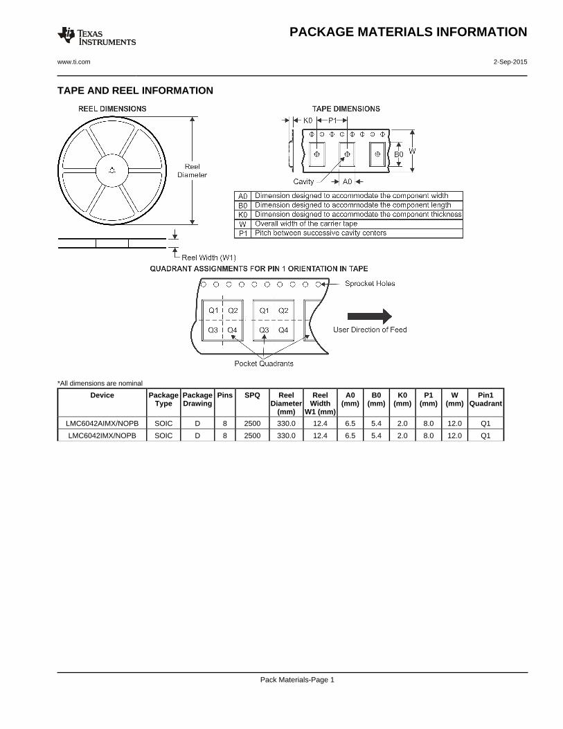
TAPE AND REEL INFORMATION
*All dimensions are nominal
Device PackageType
PackageDrawing
Pins SPQ ReelDiameter
(mm)
ReelWidth
W1 (mm)
A0(mm)
B0(mm)
K0(mm)
P1(mm)
W(mm)
Pin1Quadrant
LMC6042AIMX/NOPB SOIC D 8 2500 330.0 12.4 6.5 5.4 2.0 8.0 12.0 Q1
LMC6042IMX/NOPB SOIC D 8 2500 330.0 12.4 6.5 5.4 2.0 8.0 12.0 Q1
PACKAGE MATERIALS INFORMATION
www.ti.com 2-Sep-2015
Pack Materials-Page 1
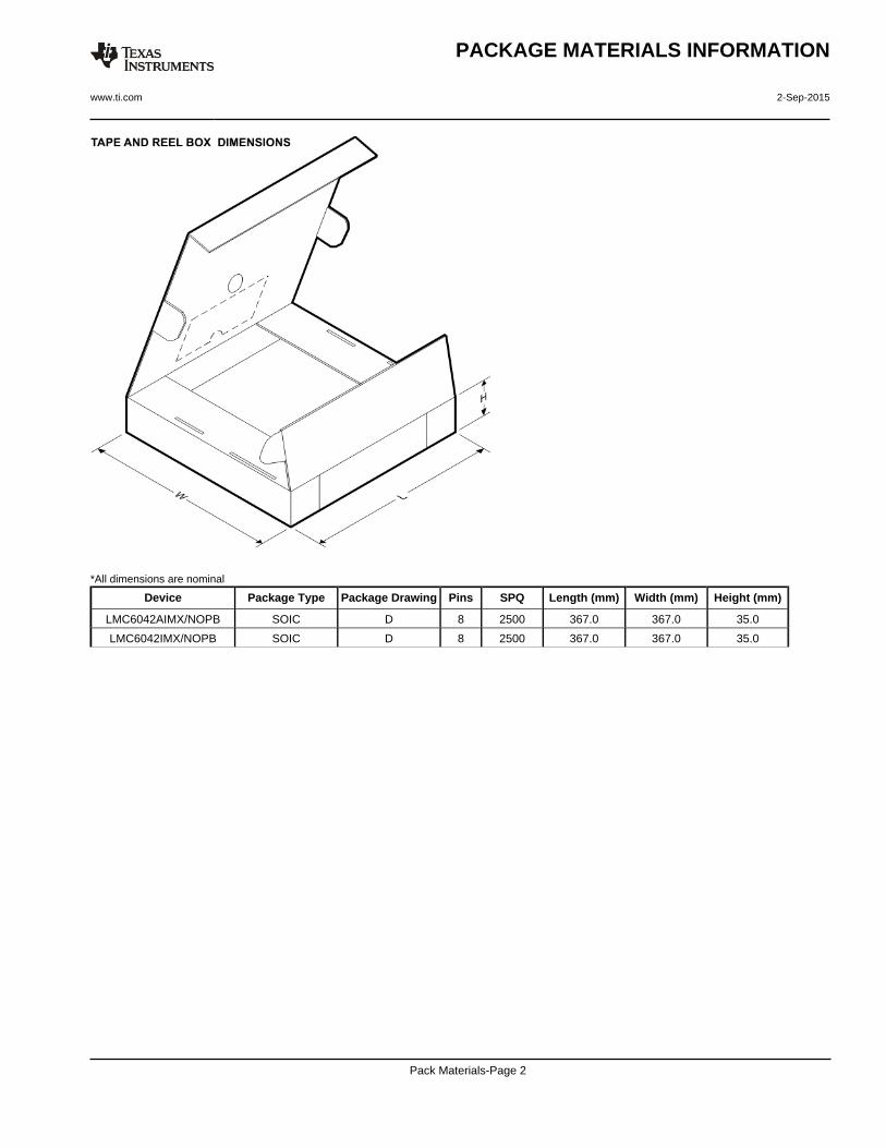
*All dimensions are nominal
Device Package Type Package Drawing Pins SPQ Length (mm) Width (mm) Height (mm)
LMC6042AIMX/NOPB SOIC D 8 2500 367.0 367.0 35.0
LMC6042IMX/NOPB SOIC D 8 2500 367.0 367.0 35.0
PACKAGE MATERIALS INFORMATION
www.ti.com 2-Sep-2015
Pack Materials-Page 2
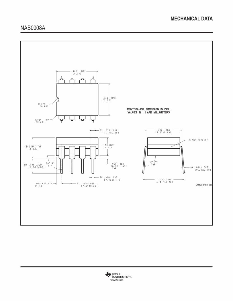
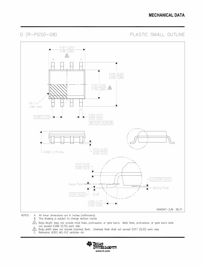
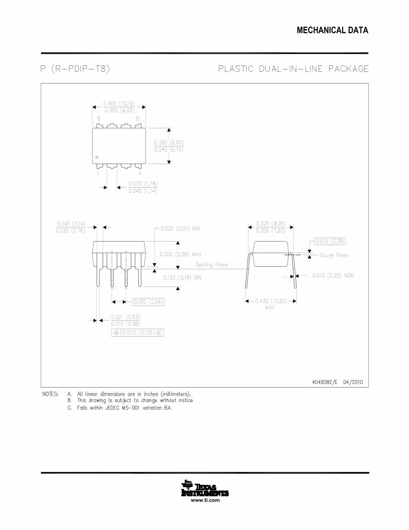
MECHANICAL DATA
NAB0008A
www.ti.com
J08A (Rev M)
IMPORTANT NOTICE
Texas Instruments Incorporated (TI) reserves the right to make corrections, enhancements, improvements and other changes to itssemiconductor products and services per JESD46, latest issue, and to discontinue any product or service per JESD48, latest issue. Buyersshould obtain the latest relevant information before placing orders and should verify that such information is current and complete.TI’s published terms of sale for semiconductor products (http://www.ti.com/sc/docs/stdterms.htm) apply to the sale of packaged integratedcircuit products that TI has qualified and released to market. Additional terms may apply to the use or sale of other types of TI products andservices.Reproduction of significant portions of TI information in TI data sheets is permissible only if reproduction is without alteration and isaccompanied by all associated warranties, conditions, limitations, and notices. TI is not responsible or liable for such reproduceddocumentation. Information of third parties may be subject to additional restrictions. Resale of TI products or services with statementsdifferent from or beyond the parameters stated by TI for that product or service voids all express and any implied warranties for theassociated TI product or service and is an unfair and deceptive business practice. TI is not responsible or liable for any such statements.Buyers and others who are developing systems that incorporate TI products (collectively, “Designers”) understand and agree that Designersremain responsible for using their independent analysis, evaluation and judgment in designing their applications and that Designers havefull and exclusive responsibility to assure the safety of Designers' applications and compliance of their applications (and of all TI productsused in or for Designers’ applications) with all applicable regulations, laws and other applicable requirements. Designer represents that, withrespect to their applications, Designer has all the necessary expertise to create and implement safeguards that (1) anticipate dangerousconsequences of failures, (2) monitor failures and their consequences, and (3) lessen the likelihood of failures that might cause harm andtake appropriate actions. Designer agrees that prior to using or distributing any applications that include TI products, Designer willthoroughly test such applications and the functionality of such TI products as used in such applications.TI’s provision of technical, application or other design advice, quality characterization, reliability data or other services or information,including, but not limited to, reference designs and materials relating to evaluation modules, (collectively, “TI Resources”) are intended toassist designers who are developing applications that incorporate TI products; by downloading, accessing or using TI Resources in anyway, Designer (individually or, if Designer is acting on behalf of a company, Designer’s company) agrees to use any particular TI Resourcesolely for this purpose and subject to the terms of this Notice.TI’s provision of TI Resources does not expand or otherwise alter TI’s applicable published warranties or warranty disclaimers for TIproducts, and no additional obligations or liabilities arise from TI providing such TI Resources. TI reserves the right to make corrections,enhancements, improvements and other changes to its TI Resources. TI has not conducted any testing other than that specificallydescribed in the published documentation for a particular TI Resource.Designer is authorized to use, copy and modify any individual TI Resource only in connection with the development of applications thatinclude the TI product(s) identified in such TI Resource. NO OTHER LICENSE, EXPRESS OR IMPLIED, BY ESTOPPEL OR OTHERWISETO ANY OTHER TI INTELLECTUAL PROPERTY RIGHT, AND NO LICENSE TO ANY TECHNOLOGY OR INTELLECTUAL PROPERTYRIGHT OF TI OR ANY THIRD PARTY IS GRANTED HEREIN, including but not limited to any patent right, copyright, mask work right, orother intellectual property right relating to any combination, machine, or process in which TI products or services are used. Informationregarding or referencing third-party products or services does not constitute a license to use such products or services, or a warranty orendorsement thereof. Use of TI Resources may require a license from a third party under the patents or other intellectual property of thethird party, or a license from TI under the patents or other intellectual property of TI.TI RESOURCES ARE PROVIDED “AS IS” AND WITH ALL FAULTS. TI DISCLAIMS ALL OTHER WARRANTIES ORREPRESENTATIONS, EXPRESS OR IMPLIED, REGARDING RESOURCES OR USE THEREOF, INCLUDING BUT NOT LIMITED TOACCURACY OR COMPLETENESS, TITLE, ANY EPIDEMIC FAILURE WARRANTY AND ANY IMPLIED WARRANTIES OFMERCHANTABILITY, FITNESS FOR A PARTICULAR PURPOSE, AND NON-INFRINGEMENT OF ANY THIRD PARTY INTELLECTUALPROPERTY RIGHTS. TI SHALL NOT BE LIABLE FOR AND SHALL NOT DEFEND OR INDEMNIFY DESIGNER AGAINST ANY CLAIM,INCLUDING BUT NOT LIMITED TO ANY INFRINGEMENT CLAIM THAT RELATES TO OR IS BASED ON ANY COMBINATION OFPRODUCTS EVEN IF DESCRIBED IN TI RESOURCES OR OTHERWISE. IN NO EVENT SHALL TI BE LIABLE FOR ANY ACTUAL,DIRECT, SPECIAL, COLLATERAL, INDIRECT, PUNITIVE, INCIDENTAL, CONSEQUENTIAL OR EXEMPLARY DAMAGES INCONNECTION WITH OR ARISING OUT OF TI RESOURCES OR USE THEREOF, AND REGARDLESS OF WHETHER TI HAS BEENADVISED OF THE POSSIBILITY OF SUCH DAMAGES.Unless TI has explicitly designated an individual product as meeting the requirements of a particular industry standard (e.g., ISO/TS 16949and ISO 26262), TI is not responsible for any failure to meet such industry standard requirements.Where TI specifically promotes products as facilitating functional safety or as compliant with industry functional safety standards, suchproducts are intended to help enable customers to design and create their own applications that meet applicable functional safety standardsand requirements. Using products in an application does not by itself establish any safety features in the application. Designers mustensure compliance with safety-related requirements and standards applicable to their applications. Designer may not use any TI products inlife-critical medical equipment unless authorized officers of the parties have executed a special contract specifically governing such use.Life-critical medical equipment is medical equipment where failure of such equipment would cause serious bodily injury or death (e.g., lifesupport, pacemakers, defibrillators, heart pumps, neurostimulators, and implantables). Such equipment includes, without limitation, allmedical devices identified by the U.S. Food and Drug Administration as Class III devices and equivalent classifications outside the U.S.TI may expressly designate certain products as completing a particular qualification (e.g., Q100, Military Grade, or Enhanced Product).Designers agree that it has the necessary expertise to select the product with the appropriate qualification designation for their applicationsand that proper product selection is at Designers’ own risk. Designers are solely responsible for compliance with all legal and regulatoryrequirements in connection with such selection.Designer will fully indemnify TI and its representatives against any damages, costs, losses, and/or liabilities arising out of Designer’s non-compliance with the terms and provisions of this Notice.
Mailing Address: Texas Instruments, Post Office Box 655303, Dallas, Texas 75265Copyright © 2017, Texas Instruments Incorporated
![Smart Sensors Laser Sensors CMOS Type ZX2 - assets.omron.eu · 2 ZX2 Ordering Information Units Sensor Heads [Dimensions page 11] Amplifier Units [Dimensions page 11] Accessories](https://img.pdfslide.tips/doc/110x75/5d56533788c993df7b8b5205/smart-sensors-laser-sensors-cmos-type-zx2-2-zx2-ordering-information-units.jpg)


![A Microcontroller-Based Lock-In Amplifier for Capacitive ...cmos 연산증폭기로써최저동작 전원전압은 2.1 v, 이득대역폭 1.5 mhz, 슬루율은 0.9 v/ s이다[11]](https://img.pdfslide.tips/doc/110x75/5e78d8af0111e2605e271bae/a-microcontroller-based-lock-in-amplifier-for-capacitive-cmos-eeoeoee.jpg)