Embed Size (px)
Citation preview
Logic Design
المنطقي التصميمSecond Course
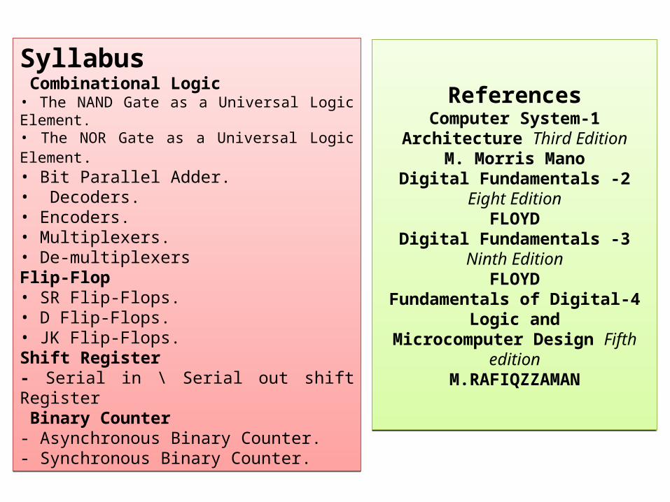
Syllabus Combinational Logic• The NAND Gate as a Universal Logic Element.• The NOR Gate as a Universal Logic Element.• Bit Parallel Adder.• Decoders.• Encoders.• Multiplexers.• De-multiplexersFlip-Flop• SR Flip-Flops.• D Flip-Flops.• JK Flip-Flops.Shift Register- Serial in \ Serial out shift Register Binary Counter- Asynchronous Binary Counter.- Synchronous Binary Counter.
Syllabus Combinational Logic• The NAND Gate as a Universal Logic Element.• The NOR Gate as a Universal Logic Element.• Bit Parallel Adder.• Decoders.• Encoders.• Multiplexers.• De-multiplexersFlip-Flop• SR Flip-Flops.• D Flip-Flops.• JK Flip-Flops.Shift Register- Serial in \ Serial out shift Register Binary Counter- Asynchronous Binary Counter.- Synchronous Binary Counter.
References1- Computer System Architecture Third
EditionM. Morris Mano
2 - Digital FundamentalsEight EditionFLOYD
3 - Digital FundamentalsNinth EditionFLOYD
4-Fundamentals of Digital Logic and Microcomputer DesignFifth edition
M.RAFIQZZAMAN
References1-Computer System Architecture Third
EditionM. Morris Mano
2 -Digital Fundamentals Eight EditionFLOYD
3 -Digital Fundamentals Ninth EditionFLOYD
4-Fundamentals of Digital Logic andMicrocomputer Design Fifth edition
M.RAFIQZZAMAN
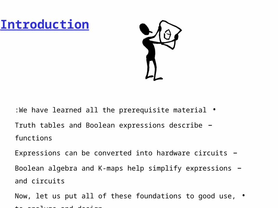
•We have learned all the prerequisite material:
–Truth tables and Boolean expressions describe functions
–Expressions can be converted into hardware circuits
–Boolean algebra and K-maps help simplify expressions and
circuits
•Now, let us put all of these foundations to good use, to analyze
and design
some larger circuits
Introduction
• Logic circuits for digital systems may be
• A combinational circuit consists of logic gates whose outputs at any
time
are determined by the current input values, i.e., it has no memory
elements
• A sequential circuit consists of logic gates whose outputs at any
time
are determined by the current input values as well as the past input
values, i.e., it has memory elements.
• Each input and output variable is a binary variable
• 2^n possible binary input combinations
• One possible binary value at the output for each input combination
• A truth table or m Boolean functions can be used to specify input-output relation
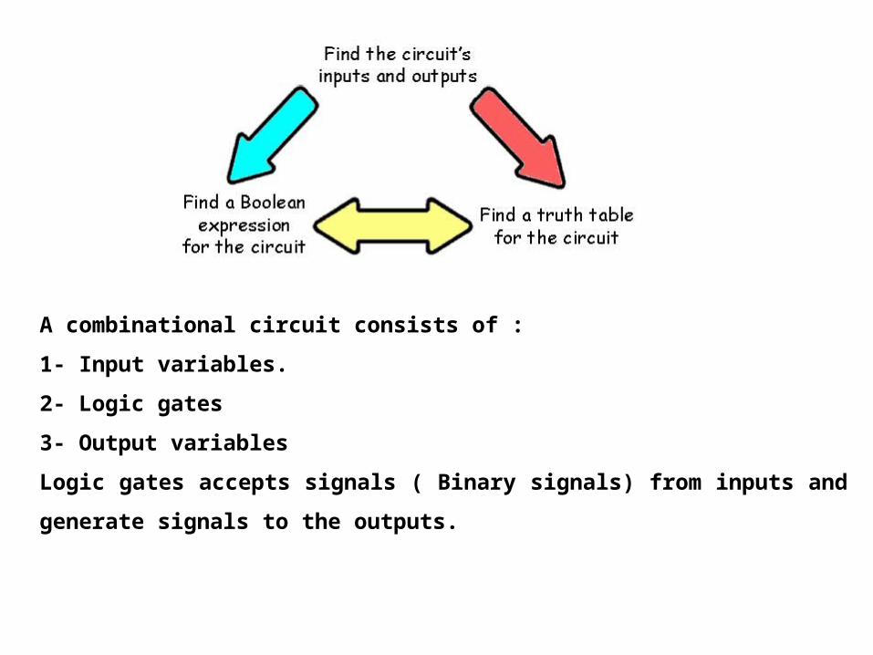
A combinational circuit consists of :
1- Input variables.
2- Logic gates
3- Output variables
Logic gates accepts signals ( Binary signals) from inputs and generate signals to the
outputs.
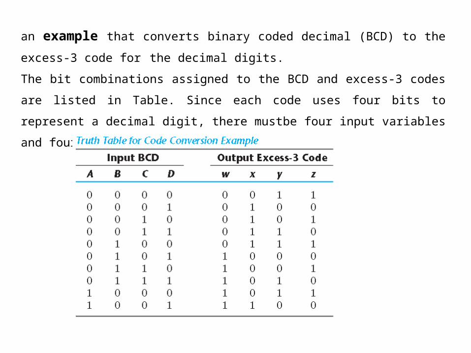
an example that converts binary coded decimal (BCD) to the excess-
3 code for the decimal digits.
The bit combinations assigned to the BCD and excess-3 codes are
listed in Table. Since each code uses four bits to represent a decimal
digit, there mustbe four input variables and four output variables.
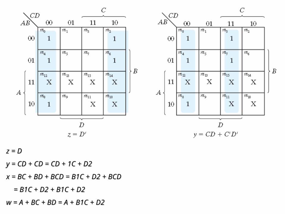
z = Dz = D
y = CD + CD = CD + 1C + D2y = CD + CD = CD + 1C + D2
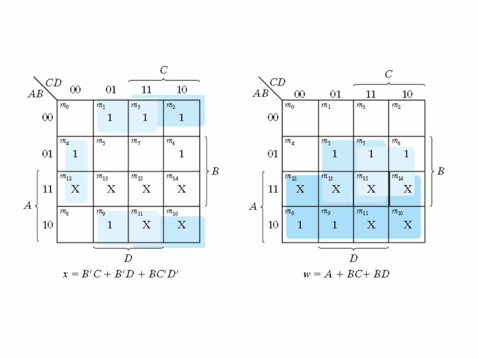
x = BC + BD + BCD = B1C + D2 + BCDx = BC + BD + BCD = B1C + D2 + BCD
= B1C + D2 + B1C + D2= B1C + D2 + B1C + D2
w = A + BC + BD = A + B1C + D2w = A + BC + BD = A + B1C + D2
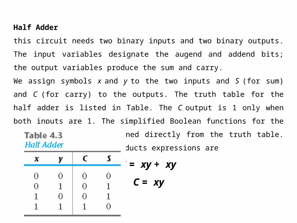
Half Adder
this circuit needs two binary inputs and two binary outputs. The input variables designate
the augend and addend bits; the output variables produce the sum and carry.
We assign symbols x and y to the two inputs and S (for sum) and C (for carry) to the
outputs. The truth table for the half adder is listed in Table. The C output is 1 only when
both inputs are 1. The simplified Boolean functions for the two outputs can be obtained
directly from the truth table. The simplified sum-of-products expressions are
S = xy + xy
C = xy
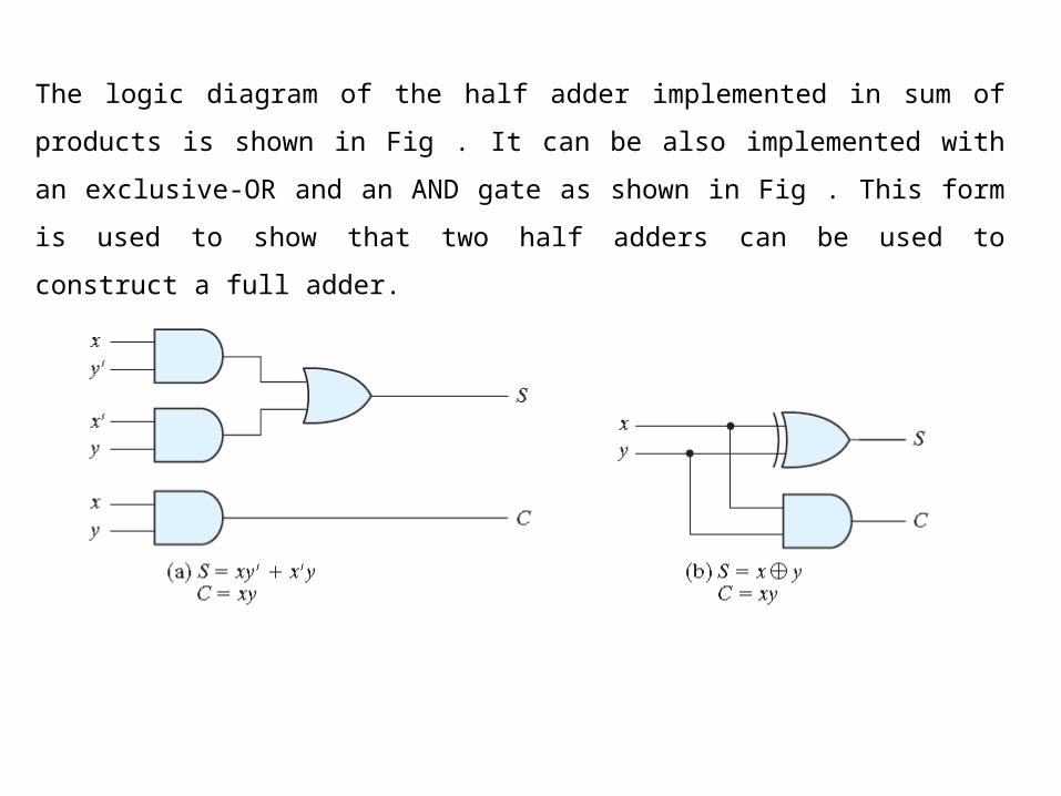
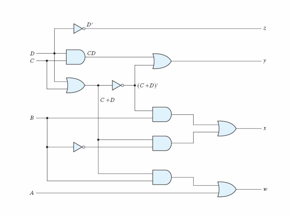
The logic diagram of the half adder implemented in sum of products is shown in Fig . It
can be also implemented with an exclusive-OR and an AND gate as shown in Fig . This
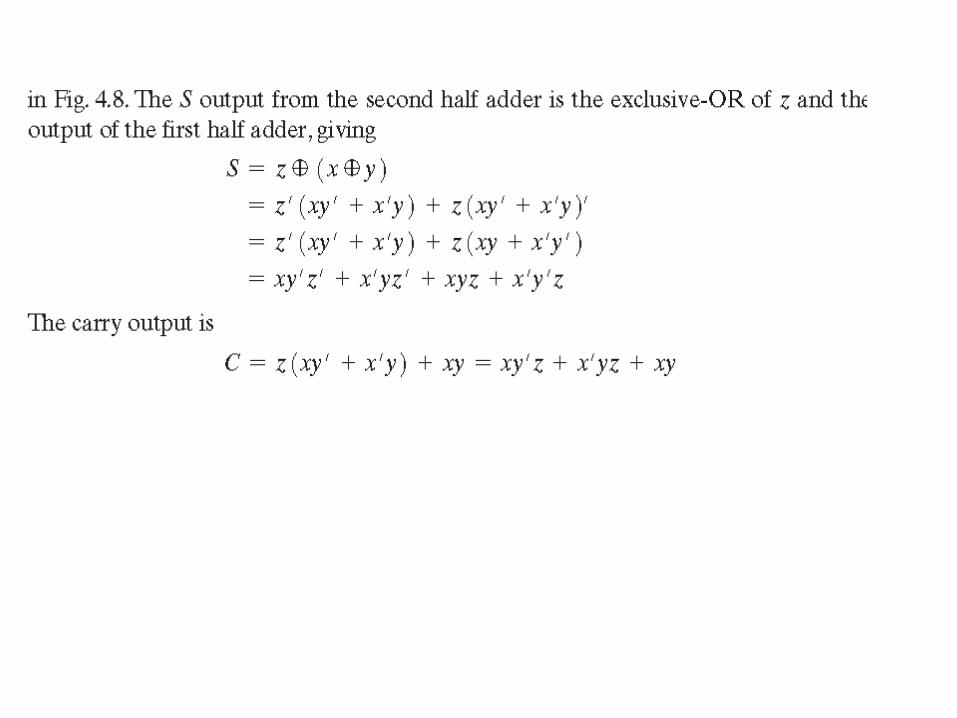
form is used to show that two half adders can be used to construct a full adder.
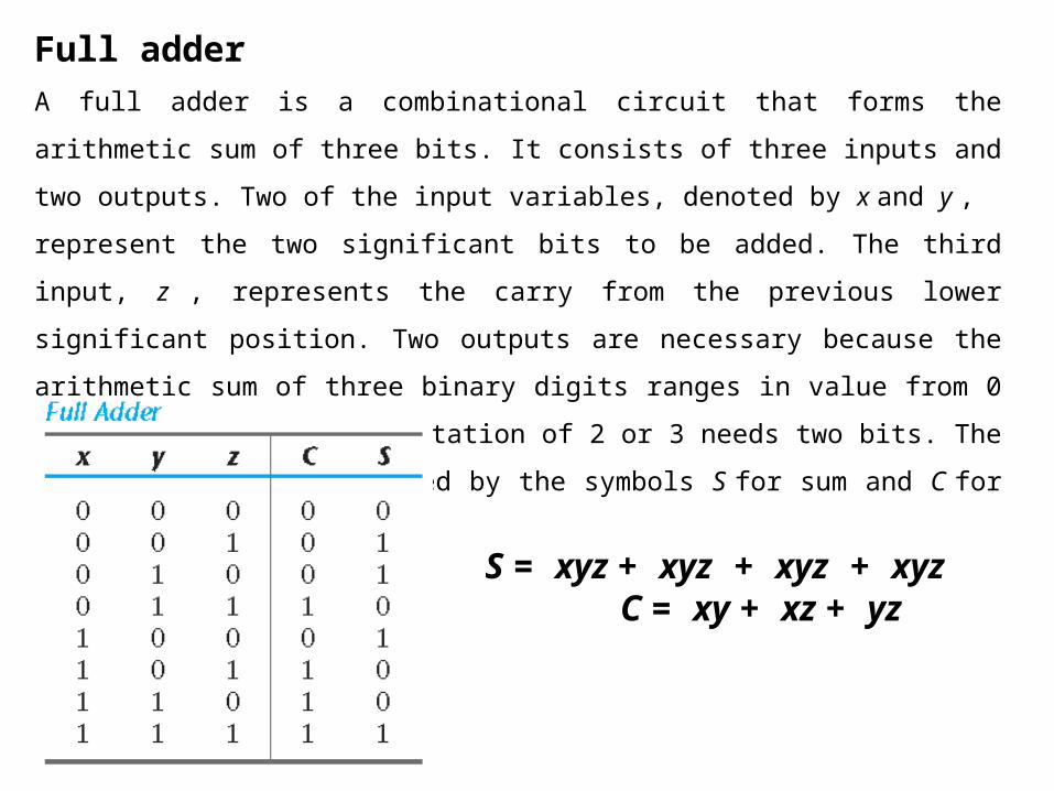
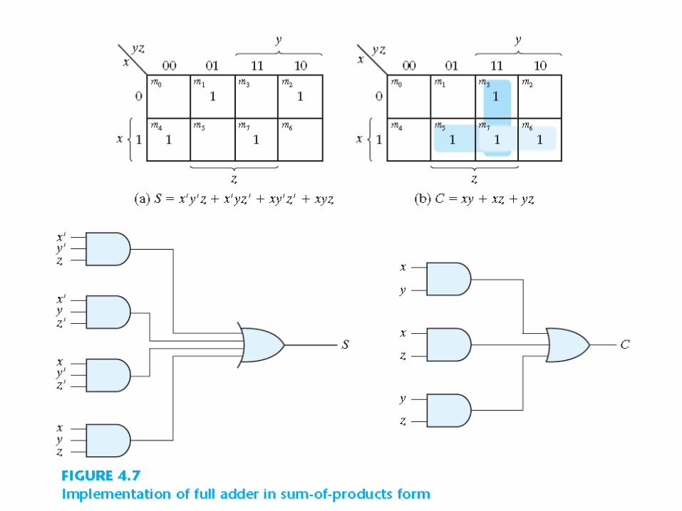
Full adderA full adder is a combinational circuit that forms the arithmetic sum of three bits. It
consists of three inputs and two outputs. Two of the input variables, denoted by x and y ,
represent the two significant bits to be added. The third input, z , represents the carry
from the previous lower significant position. Two outputs are necessary because the
arithmetic sum of three binary digits ranges in value from 0 to 3, and binary
representation of 2 or 3 needs two bits. The two outputs are designated by the symbols S
for sum and C for carry.
S = xyz + xyz + xyz + xyz C = xy + xz + yz

![DASAR-DASAR FUZZY LOGIC - Universitas Padjadjaran...Universal memuat semua elemen, sebagai contoh, Jatzen [7] a. Himpunan universal hádala manusia yang tergolong usia muda yang berjumlah](https://img.pdfslide.tips/doc/110x75/614877d22918e2056c22b57a/dasar-dasar-fuzzy-logic-universitas-padjadjaran-universal-memuat-semua-elemen.jpg)