Embed Size (px)
Citation preview
TS9004
Page 1 © 2014 Silicon Laboratories, Inc. All rights reserved.
FEATURES ♦ Ultra-Low Quiescent Current:
5.1μA (max), All comparators plus Reference ♦ Single or Dual Power Supplies:
Single: +2.5V to +11V Dual: ±1.25V to ±5.5V
♦ Input Voltage Range Includes Negative Supply ♦ 7μs Propagation Delay ♦ Push-pull TTL/CMOS-Compatible Outputs ♦ Separate Output GND Pin ♦ Crowbar-Current-Free Switching ♦ Continuous Source Current Capability: 40mA ♦ Internal 1.182V ±1% Reference ♦ 16-pin Narrow SOIC Package
APPLICATIONS Threshold Detectors Window Comparator Level Translators Oscillator Circuits Battery-Powered Systems
DESCRIPTION
The TS9004 low-voltage, micropower quad analog comparator is form-factor identical to the MAX934 analog comparator with improved electrical specifications. Ideal for 3V or 5V single-supply applications, the TS9004 draws 22% lower supply current with a 50%-better initial accuracy reference voltage. The TS9004 joins the TS9001-1/2 and TS9002 analog comparators in the “NanoWatt Analog™” high performance analog integrated circuits portfolio. This quad comparator can operate from single +2.5V to +11V supplies or from ±1.25V to ±5.5V dual supplies. The TS9004 exhibits an input voltage range from the negative supply rail to within 1.3V of the positive supply. In addition, its push-pull output stage is TTL/CMOS compatible and capable of sinking and sourcing current. It also incorporates an internal 1.182V ±1% voltage reference. A GND connection available at the TS9004’s output stage enables TTL compatibility and bipolar-to-single ended conversion. The TS9004 is fully specified over the -40ºC to +85ºC temperature range and is available in a 16-pin narrow SOIC package.
Low-Power Single/Dual-Supply Quad Comparator with Reference
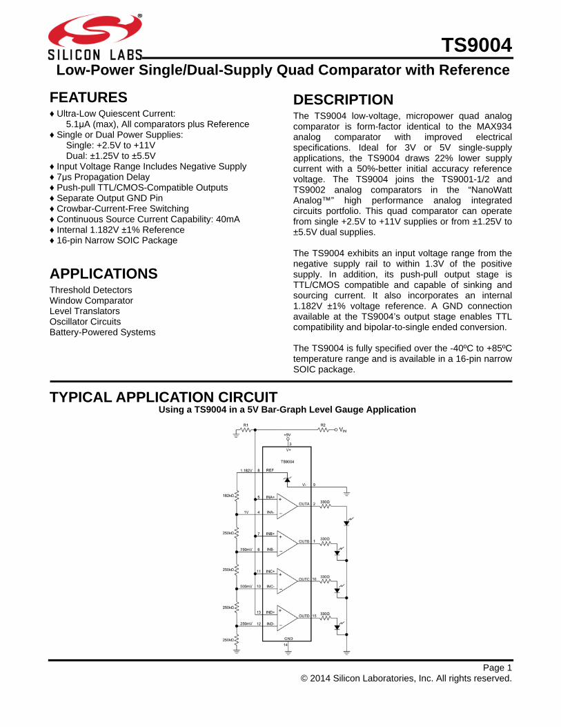
TYPICAL APPLICATION CIRCUITUsing a TS9004 in a 5V Bar-Graph Level Gauge Application
TS9004
Page 2 TS9004 Rev. 1.0
ABSOLUTE MAXIMUM RATINGSSupply Voltage (V+ to V-, V+ to GND, GND to V-)......-0.3V, +12V Voltage Inputs
(IN+, IN-)..............................................(V+ + 0.3V) to (V- - 0.3V) Output Voltage
REF..................................................... (V+ + 0.3V) to (V- - 0.3V) OUT ................................................(V+ + 0.3V) to (GND - 0.3V)
Input Current (IN+, IN-)...........................................................20mA
Continuous Power Dissipation (TA = +70°C) 16-Pin SOIC (derate 8.7mW/°C above +70°C) ................696mW
Operating Temperature Ranges..............................-40°C to +85°C Storage Temperature Range ................................-65°C to +150°C Lead Temperature (soldering, 10s) .....................................+300°C
Output Current REF…………………………………………………………….20mA OUT………………………………………………………...….40mA
Output Short-Circuit Duration (V+ ≤ 5.5V) ....................Continuous Electrical and thermal stresses beyond those listed under “Absolute Maximum Ratings” may cause permanent damage to the device. These are stress ratings only and functional operation of the device at these or any other condition beyond those indicated in the operational sections of the specifications is not implied. Exposure to any absolute maximum rating conditions for extended periods may affect device reliability and lifetime.
PACKAGE/ORDERING INFORMATION
ORDER NUMBERPART
MARKINGCARRIER QUANTITY
TS9004ISN16
TS9004I
Tube 48
TS9004ISN16T Tape
& Reel 2500
Lead-free Program: Silicon Labs supplies only lead-free packaging. Consult Silicon Labs for products specified with wider operating temperature ranges.

TS9004
TS9004 Rev. 1.0 Page 3
ELECTRICAL CHARACTERISTICS – 5V OPERATION V+ = 5V, V- = GND = 0V; TA = -40ºC to +85ºC, unless otherwise noted. Typical values are at TA = +25ºC. See Note 1.
PARAMETER CONDITIONS MIN TYP MAX UNITS POWER REQUIREMENTS Supply Voltage Range See Note 2 2.5 11 V
Supply Current IN+ = IN- + 100mV TA = +25°C 4.1 5.1
µA -40°C to +85°C 8
COMPARATOR
Input Offset Voltage VCM = 2.5V TA = +25°C ±4.5
mV -40°C to +85°C ±10
Input Leakage Current (IN-, IN+) IN+ = IN- = 2.5V TA = +25°C ±0.01 ±2
nA -40°C to +85°C ±0.01 ±5
Input Common-Mode Voltage Range V- V+ – 1.3V V Common-Mode Rejection Ratio V- to (V+ – 1.3V) 0.1 1 mV/V Power-Supply Rejection Ratio V+ = 2.5V to 11V 0.1 1 mV/V Output Voltage Noise 100Hz to 100kHz 20 μVRMS Response Time (High-to-Low Transition)
TA = +25°C, 100pF Load Overdrive = 10 mV 17
μs Overdrive = 100 mV 7
Response Time (Low-to-High Transition)
TA = +25°C, 100pF Load Overdrive = 10 mV 17
μs Overdrive = 100 mV 7
Output High Voltage -40°C to +85°C; IOUT = 17mA V+ – 0.4 V
Output Low Voltage -40°C to +85°C; IOUT = 1.8mA GND + 0.4 V Dual Supply -40°C to +85°C; IOUT = 1.8mA V- + 0.4 V
REFERENCE
Reference Voltage TA = +25°C 1.170 1.182 1.194
V -40°C to +85°C 1.158 1.206
Reference Line Regulation 2.5V ≤ (V+ - V-) ≤ 5V TA = +25°C 0.25 mV/V
Source Current ∆VREF = 1% TA = +25°C 20 25
μA -40°C to +85°C 6
Sink Current ∆VREF = 1% TA = +25°C 10 15
μA -40°C to +85°C 4
Output Voltage Noise 100Hz to 100kHz 100 μVRMS

TS9004
Page 4 TS9004 Rev. 1.0
ELECTRICAL CHARACTERISTICS – 3V OPERATION V+ = 3V, V- = GND = 0V; TA = -40ºC to +85ºC, unless otherwise noted. Typical values are at TA = +25ºC. See Note 1.
PARAMETER CONDITIONS MIN TYP MAX UNITS POWER REQUIREMENTS
Supply Current IN+ = IN- + 100mV TA = +25°C 3.8 4.8
µA -40°C to +85°C 6.5
COMPARATOR
Input Offset Voltage VCM = 1.5V TA = +25°C ±4.5
mV -40°C to +85°C ±10
Input Leakage Current (IN-, IN+) IN+ = IN- = 1.5V TA = +25°C ±0.01 ±1
nA -40°C to +85°C ±0.01 ±2.5
Input Common-Mode Voltage Range V- V+ – 1.3V V Common-Mode Rejection Ratio V- to (V+ – 1.3V) 0.2 1 mV/V Power-Supply Rejection Ratio V+ = 2.5V to 11V 0.1 1 mV/V Output Voltage Noise 100Hz to 100kHz 20 μVRMS Response Time (High-to-Low Transition)
TA = +25°C, 100pF Load Overdrive = 10 mV 17
µs Overdrive = 100 mV 7
Response Time (Low-to-High Transition)
TA = +25°C, 100pF Load Overdrive = 10 mV 17
μs Overdrive = 100 mV 7
Output High Voltage -40°C to +85°C; IOUT = 10mA V+ – 0.4 V
Output Low Voltage -40°C to +85°C; IOUT = 0.8mA GND + 0.4 V Dual Supply -40°C to +85°C; IOUT = 0.8mA V- + 0.4 V
REFERENCE
Reference Voltage TA = +25°C 1.170 1.182 1.194
V -40°C to +85°C 1.158 1.206
Reference Line Regulation 2.5V ≤ (V+ - V-) ≤ 3V TA = +25°C 0.25 mV/V
Source Current ∆VREF = 1% TA = +25°C 20 25
μA -40°C to +85°C 6
Sink Current ∆VREF = 1% TA = +25°C 10 15
μA -40°C to +85°C 4
Output Voltage Noise 100Hz to 100kHz 100 μVRMS Note 1: All specifications are 100% tested at TA = +25°C. Specification limits over temperature (TA = TMIN to TMAX) are guaranteed by device characterization, not production tested. Note 2: The TS9004 comparator operates below 2.5V. Refer to the “Low-Voltage Operation: V+ = 1.5V” section.
TS9004
TS9004 Rev. 1.0 Page 5
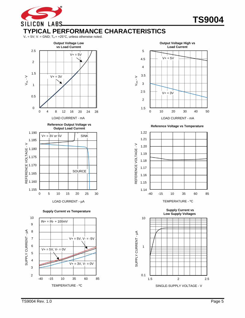
TYPICAL PERFORMANCE CHARACTERISTICS V+ = 5V; V- = GND; TA = +25°C, unless otherwise noted.
LOAD CURRENT - mA
VO
L -
V
4 8
1
0
Output Voltage Low vs Load Current
0 12
1.5
2
0.5
16
LOAD CURRENT - µA
RE
FE
RE
NC
E V
OLT
AG
E -
V
5 10
1.165
1.155
1.180
Reference Output Voltage vs Output Load Current
0 15
1.170
1.175
1.160
20
TEMPERATURE - ºC
R
EF
ER
EN
CE
VO
LTA
GE
- V
Reference Voltage vs Temperature
LOAD CURRENT - mA
VO
H -
V
10 20
2
1.5
Output Voltage High vs Load Current
0 30
2.5
40 50
3
3.5 V+ = 3V
V+ = 5V
SINK
20
2.5
4
4.5
5
V+ = 3V
V+ = 5V
25 30
1.190
1.185
SOURCE
V+ = 3V or 5V
-15 10 -40 35 60 85
1.16
1.14
1.19
1.17
1.18
1.15
1.21
1.20
1.22
24 28
TEMPERATURE - ºC
SU
PP
LY C
UR
RE
NT
- µ
A
-15 10
Supply Current vs Temperature
-40 35 60 85
4
2
5
6
3
7
8
9 IN+ = IN- + 100mV
V+ = 5V, V- = -5V
V+ = 5V, V- = 0V
V+ = 3V, V- = 0V
SINGLE-SUPPLY VOLTAGE - V
SU
PP
LY C
UR
RE
NT
- µ
A
2
1
Supply Current vs Low Supply Voltages
1.5 2.5
10
0.1
10
TS9004
Page 6 TS9004 Rev. 1.0
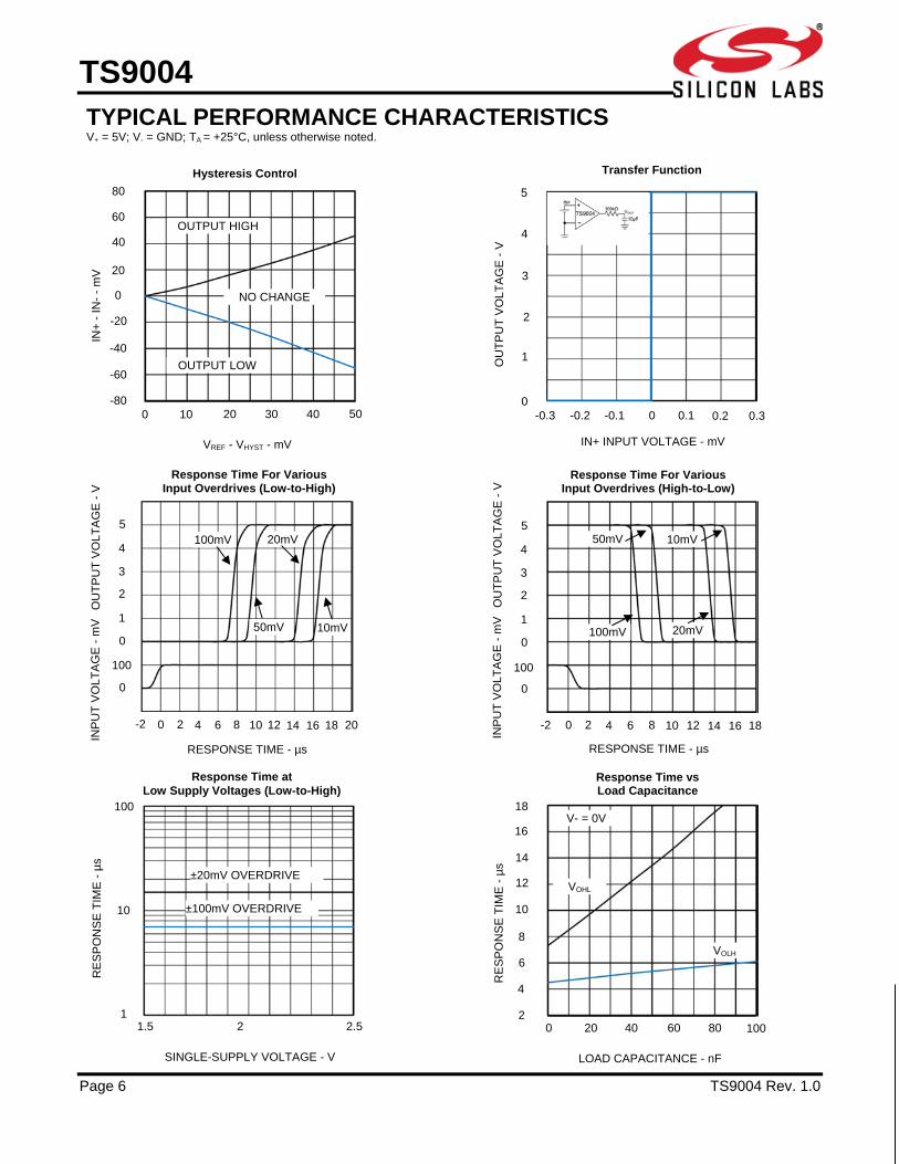
TYPICAL PERFORMANCE CHARACTERISTICS V+ = 5V; V- = GND; TA = +25°C, unless otherwise noted.
VREF - VHYST - mV
IN
+ -
IN-
- m
V
-40
-80
Hysteresis Control
-20
0
-60
10 20 0 30 40
OUTPUT HIGH
50
60
20
80
40
OUTPUT LOW
NO CHANGE
IN+ INPUT VOLTAGE - mV
OU
TP
UT
VO
LTA
GE
- V
-0.2 -0.1
1
0
Transfer Function
-0.3 0
3
4
2
0.1
LOAD CAPACITANCE - nF
R
ES
PO
NS
E T
IME
- µ
s
Response Time vs Load Capacitance
20 40 0 60 80
V- = 0V
100
6
2
8
10
4
12
14
16
18
VOHL
VOLH
RESPONSE TIME - µs
OU
TP
UT
VO
LTA
GE
- V
0 2
0
0
Response Time For Various Input Overdrives (Low-to-High)
-2 4
1
2
100
6
RESPONSE TIME - µs
Response Time For Various Input Overdrives (High-to-Low)
10mV
20mV
50mV
INP
UT
VO
LTA
GE
- m
V
OU
TP
UT
VO
LTA
GE
- V
IN
PU
T V
OLT
AG
E -
mV
8
5
3
4 100mV 10mV
20mV
50mV
100mV
10 12 14 16 18 20
0
0
1
2
100
5
3
4
0 2 -2 4 6 8 10 12 14 16 18
SINGLE-SUPPLY VOLTAGE - V
RE
SP
ON
SE
TIM
E -
µs
1.5 2
10
Response Time at Low Supply Voltages (Low-to-High)
2.5
100
1
±20mV OVERDRIVE
±100mV OVERDRIVE
0.2 0.3
5

TS9004
TS9004 Rev. 1.0 Page 7
TOTAL SUPPLY VOLTAGE - V
SO
UR
CE
CU
RR
EN
T -
mA
2.5 3.5
Short-Circuit Source Current vs Supply Voltage
1.5 4.5 5.5
TOTAL SUPPLY VOLTAGE - V
S
INK
CU
RR
EN
T -
mA
20
8
Short-Circuit Sink Current vs Supply Voltage
12
3.63 5.75 1.5
GND CONNECTED TO V-
80
0
120
160
40
200 OUT CONNECTED TO V-
OUT CONNECTED TO V+
7.88 10
16
24
TYPICAL PERFORMANCE CHARACTERISTICS V+ = 5V; V- = GND; TA = +25°C, unless otherwise noted.
SINGLE-SUPPLY VOLTAGE - V
C
UR
RE
NT
- m
A
10
Source and Sink Current at Low Supply Voltages
100
1
SOURCE CURRENT INTO 0.75V LOAD
1.5 2 2.5
SINK CURRENT ATVOUT = 0.4V

TS9004
Page 8 TS9004 Rev. 1.0
PIN FUNCTIONS
BLOCK DIAGRAM
TS9004 NAME FUNCTION
SO-16
1 OUTB Comparator B Output. Sinks and sources current. Swings from V+ to GND.
2 OUTA Comparator A Output. Sinks and sources current. Swings from V+ to GND.
3 V+ Positive Supply Voltage 4 INA- Comparator A Inverting Input 5 INA+ Comparator A Noninverting Input 6 INB- Comparator B Inverting Input 7 INB+ Comparator B Noninverting Input 8 REF 1.182V Reference Output with respect to V-.
9 V- Negative Supply Voltage. Connect to ground for single-supply operation.
10 INC- Comparator C Inverting Input 11 INC+ Comparator C Noninverting Input 12 IND- Comparator D Inverting Input 13 IND+ Comparator D Noninverting Input 14 GND Ground. Connect to V- for single-supply operation.
15 OUTD Comparator D Output. Sinks and sources current. Swings from V+ to GND.
16 OUTC Comparator C Output. Sinks and sources current. Swings from V+ to GND.

TS9004
TS9004 Rev. 1.0 Page 9
THEORY OF OPERATION The TS9004 quad, low-voltage, micropower analog comparator provides excellent flexibility and performance while sourcing continuously up to 40mA of current. The TS9004 draws 8µA (max) for all 4 comparators, including the reference. It exhibits an input offset voltage of ±4.5mV, and has an on-board +1.182V ±0.75% voltage reference. To minimize glitches that can occur with parasitic feedback or a less than optimal board layout, the design of the TS9004 output stage is optimized to eliminate crowbar glitches as the output switches. Power-Supply and Input Signal Ranges The TS9004 can operate from a single supply voltage range of +2.5V to +11V, provides a wide common mode input voltage range of V- to V+ - 1.3V, and accept input signals ranging from V- to V+ - 1V. The inputs can accept an input as much as 300mV above and below the power supply rails without damage to the part. While the TS9004 is able to operate from a single supply voltage range, a GND pin is available that allows for a dual supply operation with a range of ±1.25V to ±5.5V. If a single supply operation is desired, the GND pin needs to be tied to V-. In a dual supply mode, the TS9004 is compatible with TTL/CMOS with a ±5V voltage. Low-Voltage Operation: V+ = 1.5V The TS9004 can operate down to a supply voltage of 2V; however, as the supply voltage reduces, the TS9004 supply current drops and the performance is degraded. When the supply voltage drops to 2.2V, the reference voltage will no longer function; however, the comparators will function down to a 1V supply voltage. Furthermore, the input voltage range is extended to just below 1V the positive supply rail. For applications with a sub-2.5V power supply, it is recommended to evaluate the circuit over the entire power supply range and temperature.
Comparator Output The TS9004 has a GND pin that allows the output to swing from V+ to GND while the V- pin can be set to a voltage below GND as long as the voltage difference between V+ and V- is within 11V. Having a different voltage on V- will not affect the output swing. For TTL applications, V+ can be set to +5V±10% and V- can be set anywhere between 0V and -5V±10%. Furthermore, the output design of the TS9004 can source and sink more than 40mA and 5mA, respectively, while simultaneously maintaining a quiescent current in the microampere range. If the power dissipation of the package is maintained within the max limit, the output can source pulses of 100mA of current with V+ set to +5V. In an effort to minimize external components needed to address power supply feedback, the TS9004 output does not produce crowbar switching current as the output switches. With a 10mV input overdrive, the propagation delay of the TS9004 is 17μs. Voltage Reference The TS9004 has an on-board 1.182V reference voltage with an accuracy of ±0.75%. The REF pin is able to source and sink 20μA and 10μA of current, respectively. The REF pin is referenced to V- and it should not be bypassed. Noise Considerations Noise can play a role in the overall performance of the TS9004. Despite having a large gain, if the input voltage is near or equal to the input offset voltage, the output will randomly switch HIGH and LOW. As a result, the TS9004 produces a peak-to-peak noise of about 0.3mVPP while the reference voltage produces a peak-to-peak noise of about 1mVPP. Furthermore, it is important to design a layout that minimizes capacitive coupling from a given output to the reference pin as crosstalk can add noise and as a result, degrade performance.
APPLICATIONS INFORMATION Hysteresis As a result of circuit noise or unintended parasitic feedback, many analog comparators often break into oscillation within their linear region of operation especially when the applied differential input voltage approaches 0V (zero volt). Externally-introduced hysteresis is a well-established technique to
stabilizing analog comparator behavior and requires external components. As shown in Figure 1, adding comparator hysteresis creates two trip points: VTHR (for the rising input voltage) and VTHF (for the falling input voltage). The hysteresis band (VHB) is defined as the voltage difference between the two trip points. When a comparator’s input voltages are equal, hysteresis effectively forces one comparator input to move quickly past the other input, moving the input

TS9004
Page 10 TS9004 Rev. 1.0
out of the region where oscillation occurs. Figure 1 illustrates the case in which an IN- input is a fixed voltage and an IN+ is varied. If the input signals
were reversed, the figure would be the same with an inverted output. To add hysteresis to the TS9004, the circuit in Figure 2 is implemented and uses positive feedback along with two external resistors to set the desired hysteresis. The circuit consumes more current and it slows down the hysteresis effect
due to the high impedance on the feedback. The following procedure explains the steps to design the circuit for a desired hysteresis:
1. Choosing R3. As the leakage current at the IN+ pin is less than 1nA, the current through R3 should be at least 100nA to minimize offset voltage errors caused by the input leakage current. For R3 = 11.8MΩ, the current through R3 is VREF/R3 at the trip point. In this case, a 10MΩ resistor is a good standard value for R3.
2. Next, the desired hysteresis band (VHB) is set. In this example, VHB is set to 50mV.
3. Calculating R1.
R1 = R3 x VHB
V+
= 10MΩ x 50mV
5V
=100kΩ In this example, a 100kΩ, 1% standard value resistor is selected for R1.
4. Choose the trip point for VIN rising (VTHR),
which is the threshold voltage at which the comparator switches its output from low to high as VIN rises above the trip point. In this example, choose VTHR = 3V.
5. Calculating R2.
R2 = 1
VTHRVREF x R1 -
1R1 -
1R3
= 1
31.182V x 100kΩ -
1100kΩ -
110MΩ
=65.44kΩ
In this example, a 64.9kΩ, 1% standard value resistor is selected for R2.
6. The last step is to verify the trip voltages and hysteresis band using the standard resistance values:
VTHR = VREFx R1 x 1
R1+
1
R2+
1
R3
VTHF = VTHR – R1 x V+
R3
Board Layout and Bypassing While power-supply bypass capacitors are not typically required, it is good engineering practice to use 0.1μF bypass capacitors close to the device’s power supply pins when the power supply impedance is high, the power supply leads are long, or there is excessive noise on the power supply traces. To reduce stray capacitance, it is also good engineering practice to make signal trace lengths as short as possible. Also recommended are a ground plane and surface mount resistors and capacitors.
Figure 1. Threshold Hysteresis Band
Figure 2. External Hysteresis
TS9004
TS9004 Rev. 1.0 Page 11
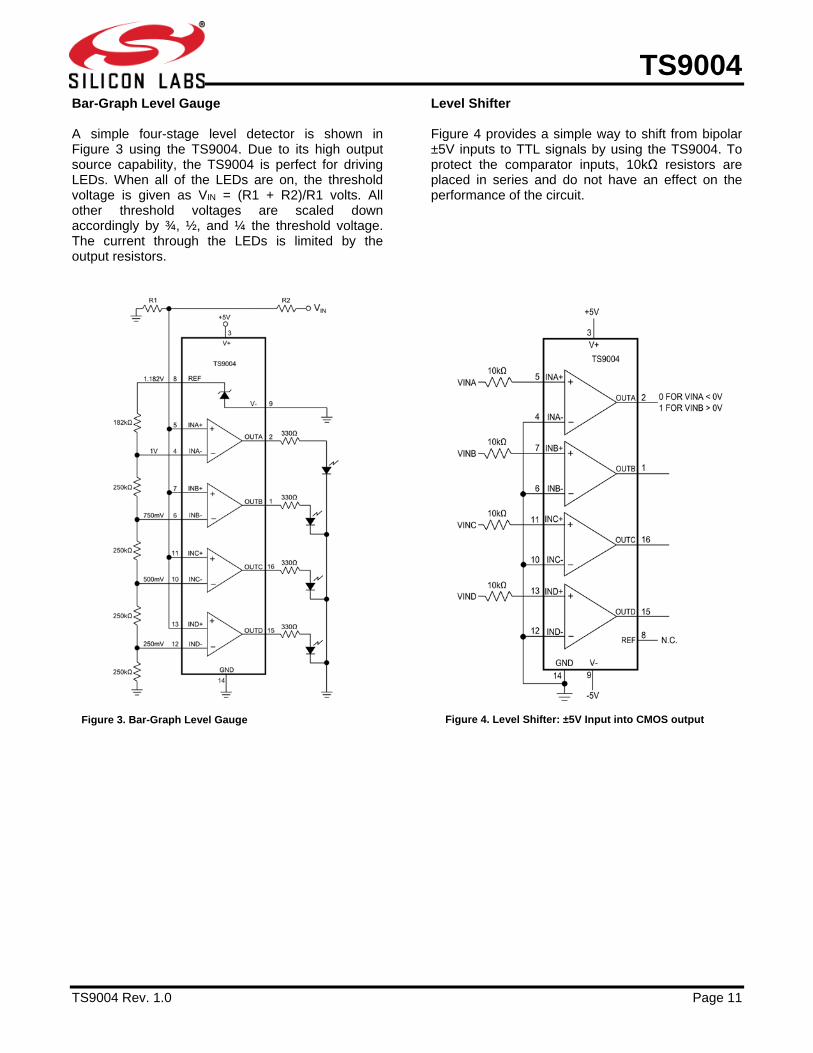
Bar-Graph Level Gauge A simple four-stage level detector is shown in Figure 3 using the TS9004. Due to its high output source capability, the TS9004 is perfect for driving LEDs. When all of the LEDs are on, the threshold voltage is given as VIN = (R1 + R2)/R1 volts. All other threshold voltages are scaled down accordingly by ¾, ½, and ¼ the threshold voltage. The current through the LEDs is limited by the output resistors.
Level Shifter Figure 4 provides a simple way to shift from bipolar ±5V inputs to TTL signals by using the TS9004. To protect the comparator inputs, 10kΩ resistors are placed in series and do not have an effect on the performance of the circuit.
Figure 3. Bar-Graph Level Gauge
Figure 4. Level Shifter: ±5V Input into CMOS output
TS9004
Page 12 Silicon Laboratories, Inc. TS9004 Rev. 1.0 400 West Cesar Chavez, Austin, TX 78701 +1 (512) 416-8500 www.silabs.com
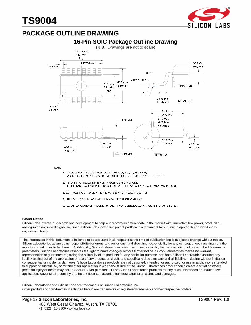
PACKAGE OUTLINE DRAWING 16-Pin SOIC Package Outline Drawing
(N.B., Drawings are not to scale)
Patent Notice Silicon Labs invests in research and development to help our customers differentiate in the market with innovative low-power, small size, analog-intensive mixed-signal solutions. Silicon Labs' extensive patent portfolio is a testament to our unique approach and world-class engineering team. The information in this document is believed to be accurate in all respects at the time of publication but is subject to change without notice. Silicon Laboratories assumes no responsibility for errors and omissions, and disclaims responsibility for any consequences resulting from the use of information included herein. Additionally, Silicon Laboratories assumes no responsibility for the functioning of undescribed features or parameters. Silicon Laboratories reserves the right to make changes without further notice. Silicon Laboratories makes no warranty, representation or guarantee regarding the suitability of its products for any particular purpose, nor does Silicon Laboratories assume any liability arising out of the application or use of any product or circuit, and specifically disclaims any and all liability, including without limitation consequential or incidental damages. Silicon Laboratories products are not designed, intended, or authorized for use in applications intended to support or sustain life, or for any other application in which the failure of the Silicon Laboratories product could create a situation where personal injury or death may occur. Should Buyer purchase or use Silicon Laboratories products for any such unintended or unauthorized application, Buyer shall indemnify and hold Silicon Laboratories harmless against all claims and damages. Silicon Laboratories and Silicon Labs are trademarks of Silicon Laboratories Inc. Other products or brandnames mentioned herein are trademarks or registered trademarks of their respective holders.

DisclaimerSilicon Laboratories intends to provide customers with the latest, accurate, and in-depth documentation of all peripherals and modules available for system and software implementers using or intending to use the Silicon Laboratories products. Characterization data, available modules and peripherals, memory sizes and memory addresses refer to each specific device, and "Typical" parameters provided can and do vary in different applications. Application examples described herein are for illustrative purposes only. Silicon Laboratories reserves the right to make changes without further notice and limitation to product information, specifications, and descriptions herein, and does not give warranties as to the accuracy or completeness of the included information. Silicon Laboratories shall have no liability for the consequences of use of the information supplied herein. This document does not imply or express copyright licenses granted hereunder to design or fabricate any integrated circuits. The products must not be used within any Life Support System without the specific written consent of Silicon Laboratories. A "Life Support System" is any product or system intended to support or sustain life and/or health, which, if it fails, can be reasonably expected to result in significant personal injury or death. Silicon Laboratories products are generally not intended for military applications. Silicon Laboratories products shall under no circumstances be used in weapons of mass destruction including (but not limited to) nuclear, biological or chemical weapons, or missiles capable of delivering such weapons.
Trademark InformationSilicon Laboratories Inc., Silicon Laboratories, Silicon Labs, SiLabs and the Silicon Labs logo, CMEMS®, EFM, EFM32, EFR, Energy Micro, Energy Micro logo and combinations thereof, "the world’s most energy friendly microcontrollers", Ember®, EZLink®, EZMac®, EZRadio®, EZRadioPRO®, DSPLL®, ISOmodem ®, Precision32®, ProSLIC®, SiPHY®, USBXpress® and others are trademarks or registered trademarks of Silicon Laboratories Inc. ARM, CORTEX, Cortex-M3 and THUMB are trademarks or registered trademarks of ARM Holdings. Keil is a registered trademark of ARM Limited. All other products or brand names mentioned herein are trademarks of their respective holders.
http://www.silabs.com
Silicon Laboratories Inc.400 West Cesar ChavezAustin, TX 78701USA
Smart.Connected.Energy-Friendly
Productswww.silabs.com/products
Qualitywww.silabs.com/quality
Support and Communitycommunity.silabs.com