Embed Size (px)
Citation preview
LT1806/LT1807
118067fc
TYPICAL APPLICATION
DESCRIPTION
325MHz, Single/Dual,Rail-to-Rail Input and Output, Low Distortion,
Low Noise Precision Op Amps
The LT®1806/LT1807 are single/dual low noise rail-to-rail input and output unity-gain stable op amps that feature a 325MHz gain-bandwidth product, a 140V/μs slew rate and a 85mA output current. They are optimized for low voltage, high performance signal conditioning systems.
The LT1806/LT1807 have a very low distortion of –80dBc at 5MHz, a low input referred noise voltage of 3.5nV/√Hz and a maximum offset voltage of 550μV that allows them to be used in high performance data acquisition systems.
The LT1806/LT1807 have an input range that includes both supply rails and an output that swings within 20mV of either supply rail to maximize the signal dynamic range in low supply applications.
The LT1806/LT1807 maintain their performance for supplies from 2.5V to 12.6V and are specifi ed at 3V, 5V and ±5V supplies. The inputs can be driven beyond the supplies without damage or phase reversal of the output.
The LT1806 is available in an 8-pin SO package with the standard op amp pinout and a 6-pin TSOT-23 package. The LT1807 features the standard dual op amp pinout and is available in 8-pin SO and MSOP packages.These devices can be used as plug-in replacements for many op amps to improve input/output range and performance.
FEATURES
APPLICATIONSn Low Voltage, High Frequency Signal Processingn Driving A/D Convertersn Rail-to-Rail Buffer Amplifi ers n Active Filters n Video Line Driver
n Gain-Bandwidth Product: 325MHzn Slew Rate: 140V/μs n Wide Supply Range: 2.5V to 12.6Vn Large Output Current: 85mA n Low Distortion, 5MHz: –80dBcn Low Voltage Noise: 3.5nV/√Hzn Input Common Mode Range Includes Both Railsn Output Swings Rail-to-Rail n Input Offset Voltage (Rail-to-Rail): 550μV Maxn Common Mode Rejection: 106dB Typn Power Supply Rejection: 105dB Typn Unity-Gain Stablen Power Down Pin (LT1806)n Operating Temperature Range: – 40°C to 85°Cn Single in SO-8 and 6-Pin Low Profi le (1mm)
ThinSOT™ Packagesn Dual in SO-8 and 8-Pin MSOP Packages
–
+
1/2 LT1807
R2909Ω
R549.9Ω
R649.9Ω
R3100Ω
VIN
R1100Ω
C1 5.6pF
C2 5.6pF
–
+
1/2 LT1807
R41k
C3470pF
LTC®1420PGA GAIN = 1VREF = 4.096V
12 BITS10Msps
+AVIN
5V
–5V
18067 TA01
–AVIN
Gain of 20 Differential A/D Driver
FREQUENCY (MHz)
0–120
AM
PL
ITU
DE
(d
B)
–100
–80
–60
–40
–20
0
1 2 3 4
18067 TA02
5
VS = 5VAV = 20fSAMPLE = 10MspsfIN = 1.4086MHzSFDR = 83dBNONAVERAGEDVIN = 200mVP-P
4096 Point FFT Response
L, LT, LTC, LTM, Linear Technology and the Linear logo are registered trademarks of Linear Technology Corporation. ThinSOT is a trademark of Linear Technology Corporation. All other trademarks are the property of their respective owners.
LT1806/LT1807
218067fc
ABSOLUTE MAXIMUM RATINGSTotal Supply Voltage (V+ to V –) ............................. 12.6VInput Voltage (Note 2) .............................................. ±VSInput Current (Note 2) ..........................................±10mAOutput Short-Circuit Duration (Note 3) ............ Indefi niteOperating Temperature Range (Note 4) ...–40°C to 85°C
(Note 1)
ORDER INFORMATIONLEAD FREE FINISH TAPE AND REEL PART MARKING PACKAGE DESCRIPTION SPECIFIED TEMPERATURE RANGE
LT1806CS6#PBF LT1806CS6#TRPBF LTNK 6-Lead Plastic TSOT-23 0°C to 70°C
LT1806IS6#PBF LT1806IS6#TRPBF LTNL 6-Lead Plastic TSOT-23 –40°C to 85°C
LT1806CS8#PBF LT1806CS8#TRPBF 1806 8-Lead Plastic SO 0°C to 70°C
LT1806IS8#PBF LT1806IS8#TRPBF 1806I 8-Lead Plastic SO –40°C to 85°C
LT1807CMS8#PBF LT1807CMS8#TRPBF LTTT 8-Lead Plastic MSOP 0°C to 70°C
LT1807IMS8#PBF LT1807IMS8#TRPBF LTTV 8-Lead Plastic MSOP –40°C to 85°C
LT1807CS8#PBF LT1807CS8#TRPBF 1807 8-Lead Plastic SO 0°C to 70°C
LT1807IS8#PBF LT1807IS8#TRPBF 1807I 8-Lead Plastic SO –40°C to 85°C
Consult LTC Marketing for parts specifi ed with wider operating temperature ranges.
Consult LTC Marketing for information on non-standard lead based fi nish parts.
For more information on lead free part marking, go to: http://www.linear.com/leadfree/ For more information on tape and reel specifi cations, go to: http://www.linear.com/tapeandreel/
OUT 1
V– 2
+IN 3
6 V+
5 SHDN
4 –IN
TOP VIEW
S6 PACKAGE6-LEAD PLASTIC TSOT-23
TJMAX = 150°C, θJA = 160°C/W (Note 9)
TOP VIEW
NC
V+
OUT
NC
SHDN
–IN
+IN
V–
S8 PACKAGE8-LEAD PLASTIC SO
1
2
3
4
8
7
6
5
–+
TJMAX = 150°C, θJA = 100°C/W (Note 9)
1
2
3
4
OUT A
–IN A
+IN A
V–
8
7
6
5
V+
OUT B
–IN B
+IN B
TOP VIEW
MS8 PACKAGE8-LEAD PLASTIC MSOP
TJMAX = 150°C, θJA = 135°C/W (Note 9)
TOP VIEW
V+
OUT B
–IN B
+IN B
OUT A
–IN A
+IN A
V–
S8 PACKAGE8-LEAD PLASTIC SO
1
2
3
4
8
7
6
5
–+
–+
TJMAX = 150°C, θJA = 100°C/W (Note 9)
PIN CONFIGURATION
Specifi ed Temperature Range (Note 5) ....–40°C to 85°C Junction Temperature ........................................... 150°CStorage Temperature Range ..................–65°C to 150°CLead Temperature (Soldering, 10 sec)................... 300°C
LT1806/LT1807
318067fc
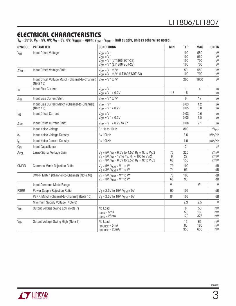
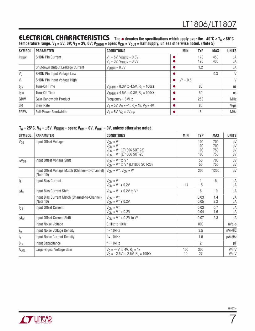
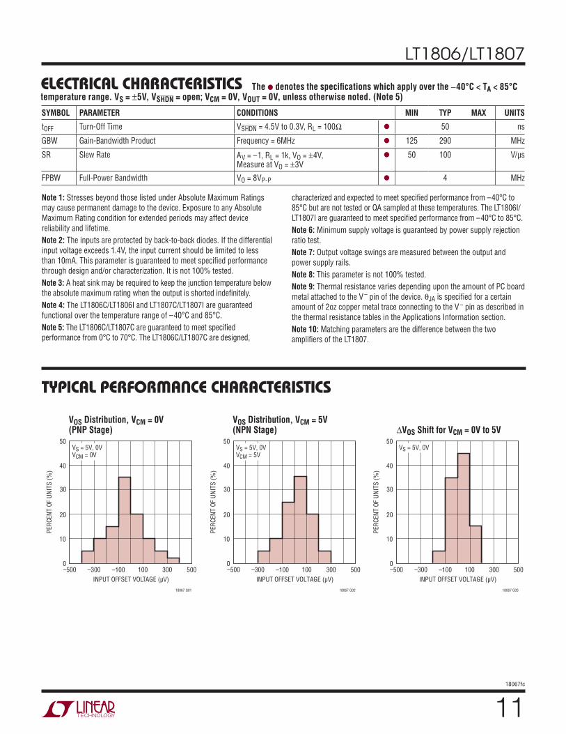
ELECTRICAL CHARACTERISTICS
SYMBOL PARAMETER CONDITIONS MIN TYP MAX UNITS
VOS Input Offset Voltage VCM = V+
VCM = V –
VCM = V+ (LT1806 SOT-23)VCM = V – (LT1806 SOT-23)
100100100100
550550700700
μVμVμVμV
ΔVOS Input Offset Voltage Shift VCM = V – to V+
VCM = V – to V+ (LT1806 SOT-23)50100
550700
μVμV
Input Offset Voltage Match (Channel-to-Channel)(Note 10)
VCM = V – to V+ 200 1000 μV
IB Input Bias Current VCM = V+
VCM = V – + 0.2V –131
–54 μA
μA
ΔIB Input Bias Current Shift VCM = V – to V+ 6 17 μA
Input Bias Current Match (Channel-to-Channel)(Note 10)
VCM = V+
VCM = V – + 0.2V0.030.05
1.23.0
μAμA
IOS Input Offset Current VCM = V+
VCM = V – + 0.2V0.030.05
0.61.5
μAμA
ΔIOS Input Offset Current Shift VCM = V – + 0.2V to V+ 0.08 2.1 μA
Input Noise Voltage 0.1Hz to 10Hz 800 nVP-P
en Input Noise Voltage Density f = 10kHz 3.5 nV/√Hz
in Input Noise Current Density f = 10kHz 1.5 pA/√Hz
CIN Input Capacitance 2 pF
AVOL Large-Signal Voltage Gain VS = 5V, VO = 0.5V to 4.5V, RL = 1k to VS/2VS = 5V, VO = 1V to 4V, RL = 100 to VS/2VS = 3V, VO = 0.5V to 2.5V, RL = 1k to VS/2
759
60
22022150
V/mVV/mVV/mV
CMRR Common Mode Rejection Ratio VS = 5V, VCM = V – to V+
VS = 3V, VCM = V – to V+7974
10095
dBdB
CMRR Match (Channel-to-Channel) (Note 10) VS = 5V, VCM = V – to V+
VS = 3V, VCM = V – to V+7368
10095
dBdB
Input Common Mode Range V – V + V
PSRR Power Supply Rejection Ratio VS = 2.5V to 10V, VCM = 0V 90 105 dB
PSRR Match (Channel-to-Channel) (Note 10) VS = 2.5V to 10V, VCM = 0V 84 105 dB
Minimum Supply Voltage (Note 6) 2.3 2.5 V
VOL Output Voltage Swing Low (Note 7) No LoadISINK = 5mAISINK = 25mA
850170
50130375
mVmVmV
VOH Output Voltage Swing High (Note 7) No LoadISOURCE = 5mAISOURCE = 25mA
1585350
65180650
mVmVmV
TA = 25°C. VS = 5V, 0V; VS = 3V, 0V; VSHDN = open; VCM = VOUT = half supply, unless otherwise noted.
LT1806/LT1807
418067fc
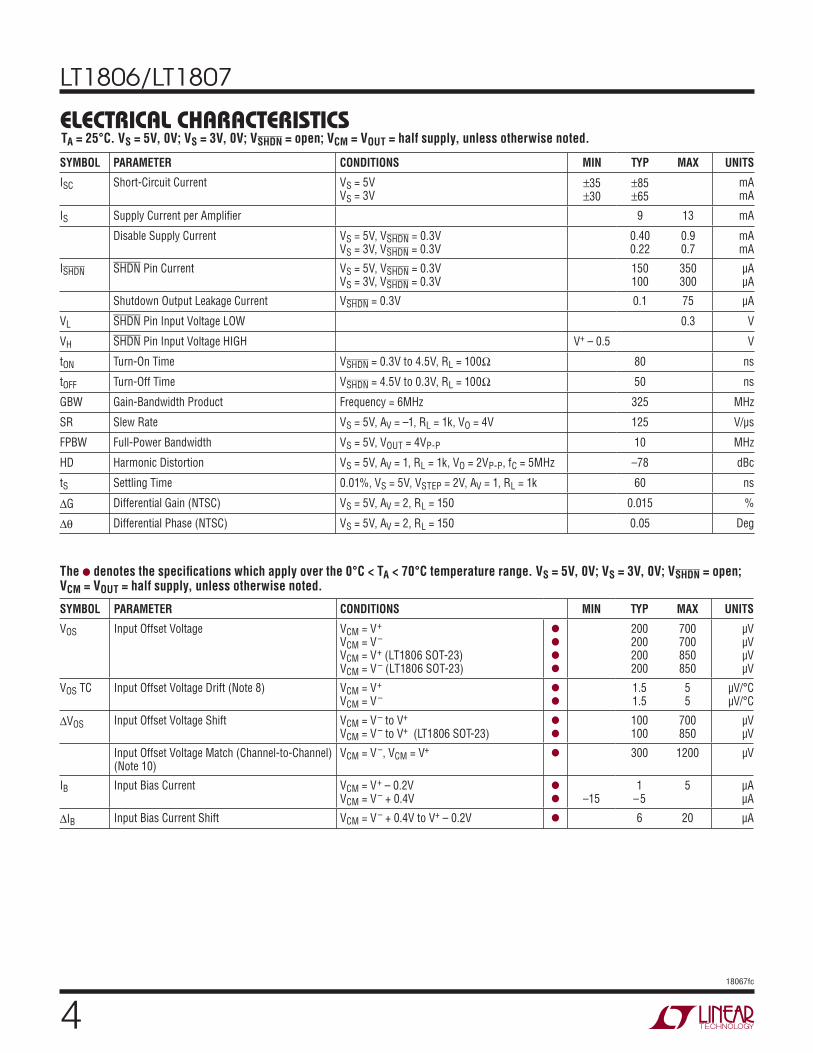
The l denotes the specifi cations which apply over the 0°C < TA < 70°C temperature range. VS = 5V, 0V; VS = 3V, 0V; VSHDN = open; VCM = VOUT = half supply, unless otherwise noted.
ELECTRICAL CHARACTERISTICSTA = 25°C. VS = 5V, 0V; VS = 3V, 0V; VSHDN = open; VCM = VOUT = half supply, unless otherwise noted.
SYMBOL PARAMETER CONDITIONS MIN TYP MAX UNITS
ISC Short-Circuit Current VS = 5VVS = 3V
±35±30
±85±65
mAmA
IS Supply Current per Amplifi er 9 13 mA
Disable Supply Current VS = 5V, VSHDN = 0.3VVS = 3V, VSHDN = 0.3V
0.400.22
0.90.7
mAmA
ISHDN SHDN Pin Current VS = 5V, VSHDN = 0.3VVS = 3V, VSHDN = 0.3V
150100
350300
μAμA
Shutdown Output Leakage Current VSHDN = 0.3V 0.1 75 μA
VL SHDN Pin Input Voltage LOW 0.3 V
VH SHDN Pin Input Voltage HIGH V+ – 0.5 V
tON Turn-On Time VSHDN = 0.3V to 4.5V, RL = 100Ω 80 ns
tOFF Turn-Off Time VSHDN = 4.5V to 0.3V, RL = 100Ω 50 ns
GBW Gain-Bandwidth Product Frequency = 6MHz 325 MHz
SR Slew Rate VS = 5V, AV = –1, RL = 1k, VO = 4V 125 V/μs
FPBW Full-Power Bandwidth VS = 5V, VOUT = 4VP-P 10 MHz
HD Harmonic Distortion VS = 5V, AV = 1, RL = 1k, VO = 2VP-P, fC = 5MHz –78 dBc
tS Settling Time 0.01%, VS = 5V, VSTEP = 2V, AV = 1, RL = 1k 60 ns
ΔG Differential Gain (NTSC) VS = 5V, AV = 2, RL = 150 0.015 %
Δθ Differential Phase (NTSC) VS = 5V, AV = 2, RL = 150 0.05 Deg
SYMBOL PARAMETER CONDITIONS MIN TYP MAX UNITS
VOS Input Offset Voltage VCM = V+
VCM = V –
VCM = V+ (LT1806 SOT-23)VCM = V – (LT1806 SOT-23)
l
l
l
l
200200200200
700700850850
μVμVμVμV
VOS TC Input Offset Voltage Drift (Note 8) VCM = V+
VCM = V –l
l
1.51.5
55
μV/°CμV/°C
ΔVOS Input Offset Voltage Shift VCM = V – to V+
VCM = V – to V+ (LT1806 SOT-23)l
l
100100
700850
μVμV
Input Offset Voltage Match (Channel-to-Channel)(Note 10)
VCM = V –, VCM = V+ l 300 1200 μV
IB Input Bias Current VCM = V+ – 0.2VVCM = V – + 0.4V
l
l –151
–55 μA
μA
ΔIB Input Bias Current Shift VCM = V – + 0.4V to V+ – 0.2V l 6 20 μA
LT1806/LT1807
518067fc
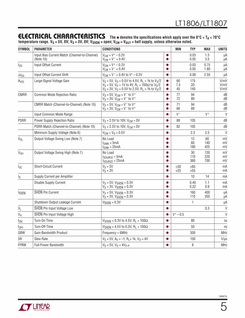
ELECTRICAL CHARACTERISTICS The l denotes the specifi cations which apply over the 0°C < TA < 70°C temperature range. VS = 5V, 0V; VS = 3V, 0V; VSHDN = open; VCM = VOUT = half supply, unless otherwise noted.
SYMBOL PARAMETER CONDITIONS MIN TYP MAX UNITS
Input Bias Current Match (Channel-to-Channel)(Note 10)
VCM = V+ – 0.2VVCM = V – + 0.4V
l
l
0.030.05
1.53.5
μAμA
IOS Input Offset Current VCM = V+ – 0.2VVCM = V – + 0.4V
l
l
0.030.05
0.751.80
μAμA
ΔIOS Input Offset Current Shift VCM = V – + 0.4V to V+ – 0.2V l 0.08 2.55 μA
AVOL Large-Signal Voltage Gain VS = 5V, VO = 0.5V to 4.5V, RL = 1k to VS/2VS = 5V, VO = 1V to 4V, RL = 100Ω to VS/2VS = 3V, VO = 0.5V to 2.5V, RL = 1k to VS/2
l
l
l
607.545
17520140
V/mVV/mVV/mV
CMRR Common Mode Rejection Ratio VS = 5V, VCM = V – to V+
VS = 3V, VCM = V – to V+l
l
7772
9489
dBdB
CMRR Match (Channel-to-Channel) (Note 10) VS = 5V, VCM = V – to V+
VS = 3V, VCM = V – to V+l
l
7166
9489
dBdB
Input Common Mode Range l V – V+ V
PSRR Power Supply Rejection Ratio VS = 2.5V to 10V, VCM = 0V l 88 105 dB
PSRR Match (Channel-to-Channel) (Note 10) VS = 2.5V to 10V, VCM = 0V l 82 105 dB
Minimum Supply Voltage (Note 6) VCM = VO = 0.5V l 2.3 2.5 V
VOL Output Voltage Swing Low (Note 7) No LoadISINK = 5mAISINK = 25mA
l
l
l
1260180
60140425
mVmVmV
VOH Output Voltage Swing High (Note 7) No LoadISOURCE = 5mAISOURCE = 25mA
l
l
l
30110360
120220700
mVmVmV
ISC Short-Circuit Current VS = 5VVS = 3V
l
l
±30±25
±65±55
mAmA
IS Supply Current per Amplifi er l 10 14 mA
Disable Supply Current VS = 5V, VSHDN = 0.3VVS = 3V, VSHDN = 0.3V
l
l
0.400.22
1.10.9
mAmA
ISHDN SHDN Pin Current VS = 5V, VSHDN = 0.3VVS = 3V, VSHDN = 0.3V
l
l
160110
400350
μAμA
Shutdown Output Leakage Current VSHDN = 0.3V l 1 μA
VL SHDN Pin Input Voltage Low l 0.3 V
VH SHDN Pin Input Voltage High l V+ – 0.5 V
tON Turn-On Time VSHDN = 0.3V to 4.5V, RL = 100Ω l 80 ns
tOFF Turn-Off Time VSHDN = 4.5V to 0.3V, RL = 100Ω l 50 ns
GBW Gain-Bandwidth Product Frequency = 6MHz l 300 MHz
SR Slew Rate VS = 5V, AV = –1, RL= 1k, VO = 4V l 100 V/μs
FPBW Full-Power Bandwidth VS = 5V, VO = 4VP-P l 8 MHz
LT1806/LT1807
618067fc
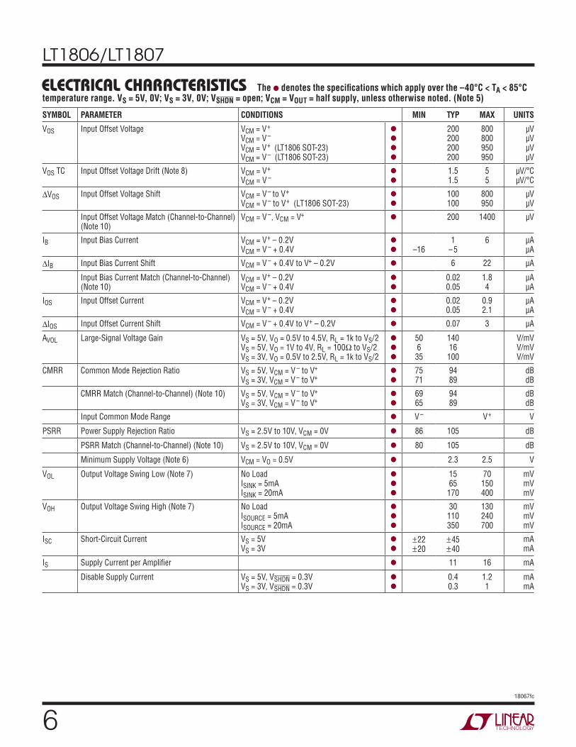
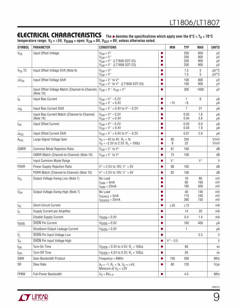
ELECTRICAL CHARACTERISTICS The l denotes the specifi cations which apply over the –40°C < TA < 85°C temperature range. VS = 5V, 0V; VS = 3V, 0V; VSHDN = open; VCM = VOUT = half supply, unless otherwise noted. (Note 5)
SYMBOL PARAMETER CONDITIONS MIN TYP MAX UNITS
VOS Input Offset Voltage VCM = V+
VCM = V –
VCM = V+ (LT1806 SOT-23)VCM = V – (LT1806 SOT-23)
l
l
l
l
200200200200
800800950950
μVμVμVμV
VOS TC Input Offset Voltage Drift (Note 8) VCM = V+
VCM = V –l
l
1.51.5
55
μV/°CμV/°C
ΔVOS Input Offset Voltage Shift VCM = V – to V+
VCM = V – to V+ (LT1806 SOT-23)l
l
100100
800950
μVμV
Input Offset Voltage Match (Channel-to-Channel)(Note 10)
VCM = V –, VCM = V+ l 200 1400 μV
IB Input Bias Current VCM = V+ – 0.2VVCM = V – + 0.4V
l
l –161
–56 μA
μA
ΔIB Input Bias Current Shift VCM = V – + 0.4V to V+ – 0.2V l 6 22 μA
Input Bias Current Match (Channel-to-Channel)(Note 10)
VCM = V+ – 0.2VVCM = V – + 0.4V
l
l
0.020.05
1.84
μAμA
IOS Input Offset Current VCM = V+ – 0.2VVCM = V – + 0.4V
l
l
0.020.05
0.92.1
μAμA
ΔIOS Input Offset Current Shift VCM = V – + 0.4V to V+ – 0.2V l 0.07 3 μA
AVOL Large-Signal Voltage Gain VS = 5V, VO = 0.5V to 4.5V, RL = 1k to VS/2VS = 5V, VO = 1V to 4V, RL = 100Ω to VS/2VS = 3V, VO = 0.5V to 2.5V, RL = 1k to VS/2
l
l
l
506
35
14016100
V/mVV/mVV/mV
CMRR Common Mode Rejection Ratio VS = 5V, VCM = V – to V+
VS = 3V, VCM = V – to V+l
l
7571
9489
dBdB
CMRR Match (Channel-to-Channel) (Note 10) VS = 5V, VCM = V – to V+
VS = 3V, VCM = V – to V+l
l
6965
9489
dBdB
Input Common Mode Range l V – V+ V
PSRR Power Supply Rejection Ratio VS = 2.5V to 10V, VCM = 0V l 86 105 dB
PSRR Match (Channel-to-Channel) (Note 10) VS = 2.5V to 10V, VCM = 0V l 80 105 dB
Minimum Supply Voltage (Note 6) VCM = VO = 0.5V l 2.3 2.5 V
VOL Output Voltage Swing Low (Note 7) No LoadISINK = 5mAISINK = 20mA
l
l
l
1565170
70150400
mVmVmV
VOH Output Voltage Swing High (Note 7) No LoadISOURCE = 5mAISOURCE = 20mA
l
l
l
30110350
130240700
mVmVmV
ISC Short-Circuit Current VS = 5VVS = 3V
l
l
±22±20
±45±40
mAmA
IS Supply Current per Amplifi er l 11 16 mA
Disable Supply Current VS = 5V, VSHDN = 0.3VVS = 3V, VSHDN = 0.3V
l
l
0.40.3
1.21
mAmA
LT1806/LT1807
718067fc
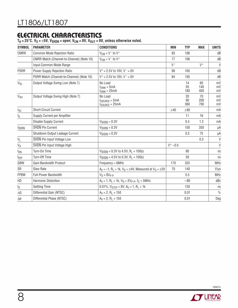
TA = 25°C. VS = ±5V, VSHDN = open; VCM = 0V, VOUT = 0V, unless otherwise noted.
SYMBOL PARAMETER CONDITIONS MIN TYP MAX UNITS
VOS Input Offset Voltage VCM = V+
VCM = V –
VCM = V+ (LT1806 SOT-23)VCM = V – (LT1806 SOT-23)
100100100100
700700750750
μVμVμVμV
ΔVOS Input Offset Voltage Shift VCM = V – to V+
VCM = V – to V+ (LT1806 SOT-23)5050
700750
μVμV
Input Offset Voltage Match (Channel-to-Channel)(Note 10)
VCM = V –, VCM = V+ 200 1200 μV
IB Input Bias Current VCM = V+
VCM = V – + 0.2V –141
–55 μA
μA
ΔIB Input Bias Current Shift VCM = V – + 0.2V to V+ 6 19 μA
Input Bias Current Match (Channel-to-Channel)(Note 10)
VCM = V+
VCM = V – + 0.2V0.030.05
1.43.2
μAμA
IOS Input Offset Current VCM = V+
VCM = V – + 0.2V0.030.04
0.71.6
μAμA
ΔIOS Input Offset Current Shift VCM = V – + 0.2V to V+ 0.07 2.3 μA
Input Noise Voltage 0.1Hz to 10Hz 800 nVp-p
en Input Noise Voltage Density f = 10kHz 3.5 nV/√Hz
in Input Noise Current Density f = 10kHz 1.5 pA/√Hz
CIN Input Capacitance f = 10kHz 2 pF
AVOL Large-Signal Voltage Gain VO = –4V to 4V, RL = 1kVO = –2.5V to 2.5V, RL = 100Ω
10010
30027
V/mVV/mV
ELECTRICAL CHARACTERISTICS The l denotes the specifi cations which apply over the –40°C < TA < 85°C temperature range. VS = 5V, 0V; VS = 3V, 0V; VSHDN = open; VCM = VOUT = half supply, unless otherwise noted. (Note 5)
SYMBOL PARAMETER CONDITIONS MIN TYP MAX UNITS
ISHDN SHDN Pin Current VS = 5V, VSHDN = 0.3VVS = 3V, VSHDN = 0.3V
l
l
170120
450400
μAμA
Shutdown Output Leakage Current VSHDN = 0.3V l 1.2 μA
VL SHDN Pin Input Voltage Low l 0.3 V
VH SHDN Pin Input Voltage High l V+ – 0.5 V
tON Turn-On Time VSHDN = 0.3V to 4.5V, RL = 100Ω l 80 ns
tOFF Turn-Off Time VSHDN = 4.5V to 0.3V, RL = 100Ω l 50 ns
GBW Gain-Bandwidth Product Frequency = 6MHz l 250 MHz
SR Slew Rate VS = 5V, AV = –1, RL= 1k, VO = 4V l 80 V/μs
FPBW Full-Power Bandwidth VS = 5V, VO = 4VP-P l 6 MHz
LT1806/LT1807
818067fc
ELECTRICAL CHARACTERISTICSTA = 25°C. VS = ±5V, VSHDN = open; VCM = 0V, VOUT = 0V, unless otherwise noted.
SYMBOL PARAMETER CONDITIONS MIN TYP MAX UNITS
CMRR Common Mode Rejection Ratio VCM = V – to V+ 83 106 dB
CMRR Match (Channel-to-Channel) (Note 10) VCM = V – to V+ 77 106 dB
Input Common Mode Range V – V+ V
PSRR Power Supply Rejection Ratio V+ = 2.5V to 10V, V – = 0V 90 105 dB
PSRR Match (Channel-to-Channel) (Note 10) V+ = 2.5V to 10V, V – = 0V 84 105 dB
VOL Output Voltage Swing Low (Note 7) No LoadISINK = 5mAISINK = 25mA
1455180
60140450
mVmVmV
VOH Output Voltage Swing High (Note 7) No LoadISOURCE = 5mAISOURCE = 25mA
2090360
70200700
mVmVmV
ISC Short-Circuit Current ±40 ±85 mA
IS Supply Current per Amplifi er 11 16 mA
Disable Supply Current VSHDN = 0.3V 0.4 1.2 mA
ISHDN SHDN Pin Current VSHDN = 0.3V 150 350 μA
Shutdown Output Leakage Current VSHDN = 0.3V 0.3 75 μA
VL SHDN Pin Input Voltage Low 0.3 V
VH SHDN Pin Input Voltage High V+ –0.5 V
tON Turn-On Time VSHDN = 0.3V to 4.5V, RL = 100Ω 80 ns
tOFF Turn-Off Time VSHDN = 4.5V to 0.3V, RL = 100Ω 50 ns
GBW Gain-Bandwidth Product Frequency = 6MHz 170 325 MHz
SR Slew Rate AV = –1, RL = 1k, VO = ±4V, Measured at VO = ±3V 70 140 V/μs
FPBW Full-Power Bandwidth VO = 8VP-P 5.5 MHz
HD Harmonic Distortion AV = 1, RL = 1k, VO = 2VP-P, fC = 5MHz –80 dBc
tS Settling Time 0.01%, VSTEP = 8V, AV = 1, RL = 1k 120 ns
ΔG Differential Gain (NTSC) AV = 2, RL = 150 0.01 %
Δθ Differential Phase (NTSC) AV = 2, RL = 150 0.01 Deg
LT1806/LT1807
918067fc
The l denotes the specifi cations which apply over the 0°C < TA < 70°C temperature range. VS = ±5V, VSHDN = open; VCM = 0V, VOUT = 0V, unless otherwise noted. ELECTRICAL CHARACTERISTICS
SYMBOL PARAMETER CONDITIONS MIN TYP MAX UNITS
VOS Input Offset Voltage VCM = V+
VCM = V –
VCM = V+ (LT1806 SOT-23)VCM = V – (LT1806 SOT-23)
l
l
l
l
200200200200
800800900900
μVμVμVμV
VOS TC Input Offset Voltage Drift (Note 8) VCM = V+
VCM = V –l
l
1.51.5
55
μV/°CμV/°C
ΔVOS Input Offset Voltage Shift VCM = V – to V+
VCM = V – to V+ (LT1806 SOT-23)l
l
100100
800900
μVμV
Input Offset Voltage Match (Channel-to-Channel)(Note 10)
VCM = V –, VCM = V+ l 300 1400 μV
IB Input Bias Current VCM = V+ – 0.2VVCM = V – + 0.4V
l
l –151
–66 μA
μA
ΔIB Input Bias Current Shift VCM = V – + 0.4V to V+ – 0.2V l 7 21 μA
Input Bias Current Match (Channel-to-Channel)(Note 10)
VCM = V+ – 0.2VVCM = V – + 0.4V
l
l
0.030.04
1.83.8
μAμA
IOS Input Offset Current VCM = V+ – 0.2VVCM = V – + 0.4V
l
l
0.030.04
0.91.9
μAμA
ΔIOS Input Offset Current Shift VCM = V – + 0.4V to V+ – 0.2V l 0.07 2.8 μA
AVOL Large-Signal Voltage Gain VO = –4V to 4V, RL = 1kVO = –2.5V to 2.5V, RL = 100Ω
l
l
808
25025
V/mVV/mV
CMRR Common Mode Rejection Ratio VCM = V – to V+ l 81 100 dB
CMRR Match (Channel-to-Channel) (Note 10) VCM = V – to V+ l 75 100 dB
Input Common Mode Range l V – V+ V
PSRR Power Supply Rejection Ratio V+ = 2.5V to 10V, V – = 0V l 88 105 dB
PSRR Match (Channel-to-Channel) (Note 10) V+ = 2.5V to 10V, V – = 0V l 82 106 dB
VOL Output Voltage Swing Low (Note 7) No LoadISINK = 5mAISINK = 25mA
l
l
l
1860185
80160500
mVmVmV
VOH Output Voltage Swing High (Note 7) No LoadISOURCE = 5mAISOURCE = 25mA
l
l
l
40110360
140240750
mVmVmV
ISC Short-Circuit Current l ±35 ±75 mA
IS Supply Current per Amplifi er l 14 20 mA
Disable Supply Current VSHDN = 0.3V l 0.4 1.4 mA
ISHDN SHDN Pin Current VSHDN = 0.3V l 160 400 μA
Shutdown Output Leakage Current VSHDN = 0.3V l 1 μA
VL SHDN Pin Input Voltage Low l 0.3 V
VH SHDN Pin Input Voltage High l V+ – 0.5 V
tON Turn-On Time VSHDN = 0.3V to 4.5V, RL = 100Ω l 80 ns
tOFF Turn-Off Time VSHDN = 4.5V to 0.3V, RL = 100Ω l 50 ns
GBW Gain-Bandwidth Product Frequency = 6MHz l 150 300 MHz
SR Slew Rate AV = –1, RL = 1k, VO = ±4V, Measure at VO = ±3V
l 60 120 V/μs
FPBW Full-Power Bandwidth VO = 8VP-P l 4.5 MHz
LT1806/LT1807
1018067fc
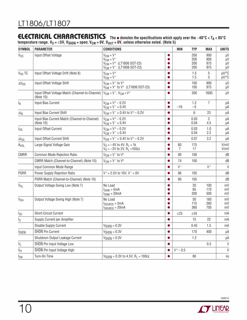
ELECTRICAL CHARACTERISTICS The l denotes the specifi cations which apply over the −40°C < TA < 85°C temperature range. VS = ±5V, VSHDN = open; VCM = 0V, VOUT = 0V, unless otherwise noted. (Note 5)
SYMBOL PARAMETER CONDITIONS MIN TYP MAX UNITS
VOS Input Offset Voltage VCM = V+
VCM = V –
VCM = V+ (LT1806 SOT-23)VCM = V – (LT1806 SOT-23)
l
l
l
l
200200200200
900900975975
μVμVμVμV
VOS TC Input Offset Voltage Drift (Note 8) VCM = V+
VCM = V –l
l
1.51.5
55
μV/°CμV/°C
ΔVOS Input Offset Voltage Shift VCM = V – to V+
VCM = V – to V+ (LT1806 SOT-23)l
l
100100
900975
μVμV
Input Offset Voltage Match (Channel-to-Channel)(Note 10)
VCM = V –, VCM = V+ l 300 1600 μV
IB Input Bias Current VCM = V+ – 0.2VVCM = V – + 0.4V
l
l –161.2–5
7 μAμA
ΔIB Input Bias Current Shift VCM = V – + 0.4V to V+ – 0.2V l 6 23 μA
Input Bias Current Match (Channel-to-Channel)(Note 10)
VCM = V+ – 0.2VVCM = V – + 0.4V
l
l
0.030.04
24.5
μAμA
IOS Input Offset Current VCM = V+ – 0.2VVCM = V – + 0.4V
l
l
0.030.04
1.02.2
μAμA
ΔIOS Input Offset Current Shift VCM = V – + 0.4V to V+ – 0.2V l 0.07 3.2 μA
AVOL Large-Signal Voltage Gain VO = –4V to 4V, RL = 1kVO = –2V to 2V, RL =100Ω
l
l
607
17517
V/mVV/mV
CMRR Common Mode Rejection Ratio VCM = V – to V+ l 80 100 dB
CMRR Match (Channel-to-Channel) (Note 10) VCM = V – to V+ l 74 100 dB
Input Common Mode Range l V – V+ V
PSRR Power Supply Rejection Ratio V+ = 2.5V to 10V, V – = 0V l 86 105 dB
PSRR Match (Channel-to-Channel) (Note 10) l 80 105 dB
VOL Output Voltage Swing Low (Note 7) No LoadISINK = 5mAISINK = 20mA
l
l
l
2065200
100170500
mVmVmV
VOH Output Voltage Swing High (Note 7) No LoadISOURCE = 5mAISOURCE = 20mA
l
l
l
50115360
160260700
mVmVmV
ISC Short-Circuit Current l ±25 ±55 mA
IS Supply Current per Amplifi er l 15 22 mA
Disable Supply Current VSHDN = 0.3V l 0.45 1.5 mA
ISHDN SHDN Pin Current VSHDN = 0.3V l 170 400 μA
Shutdown Output Leakage Current VSHDN = 0.3V l 1.2 μA
VL SHDN Pin Input Voltage Low l 0.3 V
VH SHDN Pin Input Voltage High l V+ – 0.5 V
tON Turn-On Time VSHDN = 0.3V to 4.5V, RL = 100Ω l 80 ns
LT1806/LT1807
1118067fc
Note 1: Stresses beyond those listed under Absolute Maximum Ratings
may cause permanent damage to the device. Exposure to any Absolute
Maximum Rating condition for extended periods may affect device
reliability and lifetime.
Note 2: The inputs are protected by back-to-back diodes. If the differential
input voltage exceeds 1.4V, the input current should be limited to less
than 10mA. This parameter is guaranteed to meet specifi ed performance
through design and/or characterization. It is not 100% tested.
Note 3: A heat sink may be required to keep the junction temperature below
the absolute maximum rating when the output is shorted indefi nitely.
Note 4: The LT1806C/LT1806I and LT1807C/LT1807I are guaranteed
functional over the temperature range of –40°C and 85°C.
Note 5: The LT1806C/LT1807C are guaranteed to meet specifi ed
performance from 0°C to 70°C. The LT1806C/LT1807C are designed,
characterized and expected to meet specifi ed performance from –40°C to
85°C but are not tested or QA sampled at these temperatures. The LT1806I/
LT1807I are guaranteed to meet specifi ed performance from –40°C to 85°C.
Note 6: Minimum supply voltage is guaranteed by power supply rejection
ratio test.
Note 7: Output voltage swings are measured between the output and
power supply rails.
Note 8: This parameter is not 100% tested.
Note 9: Thermal resistance varies depending upon the amount of PC board
metal attached to the V – pin of the device. θJA is specifi ed for a certain
amount of 2oz copper metal trace connecting to the V – pin as described in
the thermal resistance tables in the Applications Information section.
Note 10: Matching parameters are the difference between the two
amplifi ers of the LT1807.
ELECTRICAL CHARACTERISTICS The l denotes the specifi cations which apply over the −40°C < TA < 85°C temperature range. VS = ±5V, VSHDN = open; VCM = 0V, VOUT = 0V, unless otherwise noted. (Note 5)
SYMBOL PARAMETER CONDITIONS MIN TYP MAX UNITS
tOFF Turn-Off Time VSHDN = 4.5V to 0.3V, RL = 100Ω l 50 ns
GBW Gain-Bandwidth Product Frequency = 6MHz l 125 290 MHz
SR Slew Rate AV = –1, RL = 1k, VO = ±4V, Measure at VO = ±3V
l 50 100 V/μs
FPBW Full-Power Bandwidth VO = 8VP-P l 4 MHz
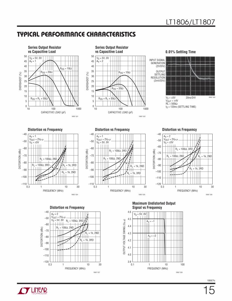
TYPICAL PERFORMANCE CHARACTERISTICS
INPUT OFFSET VOLTAGE (μV)
–500
PER
CEN
T O
F U
NIT
S (
%)
30
40
50
300
18067 G01
20
10
0–300 –100 100 500
VS = 5V, 0VVCM = 0V
INPUT OFFSET VOLTAGE (μV)
–500
PER
CEN
T O
F U
NIT
S (
%)
30
40
50
300
18067 G02
20
10
0–300 –100 100 500
VS = 5V, 0VVCM = 5V
INPUT OFFSET VOLTAGE (μV)
–500
PER
CEN
T O
F U
NIT
S (
%)
30
40
50
300
18067 G03
20
10
0–300 –100 100 500
VS = 5V, 0V
VOS Distribution, VCM = 0V(PNP Stage)
VOS Distribution, VCM = 5V(NPN Stage) ΔVOS Shift for VCM = 0V to 5V
LT1806/LT1807
1218067fc
TOTAL SUPPLY VOLTAGE (V)
1.0–1.0
CH
AN
GE I
N O
FFS
ET V
OLTA
GE (
mV
)
–0.8
–0.4
–0.2
0
1.0
0.4
2.0 3.0 3.5
18067 G10
–0.6
0.6
0.8
0.2
1.5 2.5 4.0 4.5 5.0
TA = 125°C
TA = –55°C
TA = 25°C
POWER SUPPLY VOLTAGE ( V)
1.5
OU
TP
UT S
HO
RT-C
IRC
UIT
CU
RR
EN
T (
mA
)
–40
80
100
120
2.5 3.5 4.0
18067 G11
–80
40
0
–60
60
–100
20
–20
2.0 3.0 4.5 5.0
TA = –55°C
TA = –55°C
TA = 125°C
TA = 25°C
“SINKING”
“SOURCING”
TA = 125°C
TA = 25°C
SHDN PIN VOLTAGE (V)
00
SU
PP
LY
CU
RR
EN
T (
mA
)
2
6
8
10
2 4 5
18
18067 G12
4
1 3
12
14
16
TA = 125°C
TA = –55°C
TA = 25°C
VS = 5V, 0V
Minimum Supply VoltageOutput Short-Circuit Currentvs Power Supply Voltage
Supply Currentvs SHDN Pin Voltage
TYPICAL PERFORMANCE CHARACTERISTICS
TOTAL SUPPLY VOLTAGE (V)
0
SU
PP
LY
CU
RR
EN
T (
mA
)
12
18067 G04
3 4 521 6 7 8 9 10 11
20
15
10
5
0
TA = 125°C
TA = 25°C
TA = –55°C
INPUT COMMON MODE VOLTAGE (V)
0
OFF
SET V
OLTA
GE (
μV
)
100
300
500
4
18067 G05
–100
–300
0
200
400
–200
–400
–5001 2 3 5
TA = 125°C
TA = –55°C
TA = 25°C
VS = 5V, 0VTYPICAL PART
COMMON MODE VOLTAGE (V)
–1–10
INP
UT B
IAS
CU
RR
EN
T (
μA
)
–5
0
5
0 1 2 3
18067 G06
4 5 6
TA = 125°C
TA = 25°C
TA = –55°C
VS = 5V, 0V
TA = 125°C
TA = 25°C
TA = –55°C
Supply Current per Amp vs Supply Voltage
Offset Voltagevs Input Common Mode
Input Bias Current vs Common Mode Voltage
TEMPERATURE (°C)
–50–8
INP
UT B
IAS
(μA
)
–7
–5
–4
–3
2
–1
–20 10 25 85
18067 G07
–6
0
1
–2
–35 –5 40 55 70
NPN ACTIVEVS = 5V, 0VVCM = 5V
PNP ACTIVEVS = 5V, 0VVCM = 0V
LOAD CURRENT (mA)
0.010.001
OU
TP
UT S
ATU
RA
TIO
N V
OLTA
GE (
V)
0.1
10
0.1 1 10 100
18067 G08
0.01
1
VS = 5V
TA = 125°C
TA = 25°CTA = –55°C
LOAD CURRENT (mA)
0.010.001
OU
TP
UT S
ATU
RA
TIO
N V
OLTA
GE (
V)
0.1
10
1 1000.1 10
18067 G09
0.01
1
TA = 125°C
TA = –55°C
TA = 25°C
VS = 5V
Input Bias Current vs TemperatureOutput Saturation Voltagevs Load Current (Output Low)
Output Saturation Voltagevs Load Current (Output High)
LT1806/LT1807
1318067fc
TYPICAL PERFORMANCE CHARACTERISTICS
SHDN PIN VOLTAGE (V)
0
SH
DN
PIN
CU
RR
EN
T (
μA
)
–60
–20
20
4
18067 G13
–100
–140
–80
–40
0
–120
–160
–1801 2 3 5
TA = 125°C
TA = –55°C
TA = 25°C
VS = 5V, 0V
OUTPUT VOLTAGE (V)
0–500
INP
UT V
OLTA
GE (
μV
)
–300
–100
100
0.5 1.0 1.5 2.0
18067 G14
2.5
300
500
–400
–200
0
200
400
3.0
RL = 1k
RL = 100Ω
VS = 3V, 0VRL TO GND
OUTPUT VOLTAGE (V)
0–500
INP
UT V
OLTA
GE (
μV
)
–300
–100
100
0.5 1.0 1.5 2.0
18067 G15
2.5
300
500
–400
–200
0
200
400
3.0 3.5 4.0 4.5 5.0
RL = 1k
RL = 100Ω
VS = 5V, 0VRL TO GND
SHDN Pin Currentvs SHDN Pin Voltage Open-Loop Gain Open-Loop Gain
OUTPUT VOLTAGE (V)
–5–500
INP
UT V
OLTA
GE (
μV
)
–300
–100
100
–4 –3 –2 –1
18067 G16
0
300
500
–400
–200
0
200
400
1 2 3 4 5
RL = 1k
RL = 100Ω
VS = 5V
OUTPUT CURRENT (mA)
–100–2.5
OFF
SET V
OLTA
GE (
mV
)
–1.5
–0.5
0.5
–80 –60 –40 –20
18067 G17
0
1.5
2.5
–2.0
–1.0
0
1.0
2.0
20 40 60 80 100
TA = 125°C
TA = –55°C
TA = 25°C
VS = 5V
TIME AFTER POWER-UP (SEC)
0
OFF
SET V
OLTA
GE D
RIF
T (
μV
)25
30
35
16014012010080
18067 G18
20
15
020 40 60
10
5
45
40
VS = 5V
VS = 2.5V
VS = 1.5V
Open-Loop Gain Offset Voltage vs Output CurrentWarm-Up Drift vs Time (LT1806S8)
FREQUENCY (kHz)
0.10
8
10
12
1 10 100
18067 G19
6
4
2
NO
ISE V
OLTA
GE (
nV
/H
z)
VS = 5V, 0V
NPN ACTIVEVCM = 4.5V
PNP ACTIVEVCM = 2.5V
FREQUENCY (kHz)
0.10
8
10
12
1 10 100
18067 G19
6
4
2
NO
ISE C
UR
REN
T (
pA
/H
z)
VS = 5V, 0V
NPN ACTIVEVCM = 4.5V
PNP ACTIVEVCM = 2.5V
TIME (SEC)
0
OU
TP
UT V
OLTA
GE (
nV
)
200
600
1000
8
18067 G21
–200
–600
0
400
800
–400
–800
–100021 43 6 7 95 10
Input Noise Voltage vs Frequency Input Noise Current vs Frequency0.1Hz to 10HzOutput Voltage Noise
LT1806/LT1807
1418067fc
FREQUENCY (Hz)
100k0.001
OU
TP
UT I
MP
ED
AN
CE (
Ω)
0.01
0.1
1
10
100
600
1M 10M 100M 500M
18067 G28
VS = 5V, 0V
AV = 10
AV = 2
AV = 1
FREQUENCY (MHz)
0.01
40
CO
MM
ON
MO
DE R
EJE
CTIO
N R
ATIO
(dB
)
50
60
70
80
0.1 1 10 100 500
18067 G29
30
20
10
0
90
100VS = 5V, 0V
FREQUENCY (MHz)
0.001
40
PO
WE
R S
UP
PLY
REJE
CTIO
N R
ATIO
(dB
)
50
60
70
80
0.01 0.1 1 10 100
18067 G30
30
20
10
0
90
100VS = 5V, 0VTA = 25°C
NEGATIVE SUPPLY
POSITIVE SUPPLY
Output Impedance vs FrequencyCommon Mode Rejection Ratiovs Frequency
Power Supply Rejection Ratiovs Frequency
TYPICAL PERFORMANCE CHARACTERISTICS
TOTAL SUPPLY VOLTAGE (V)
0
GA
IN B
AN
DW
IDTH
(M
Hz) P
HA
SE M
AR
GIN
(DEG
)
8
18067 G22
400
300
350
250
200
35
45
55
30
40
50
21 43 6 7 95 10
TA = 25°C
PHASE MARGIN
GAIN BANDWIDTH PRODUCT
TEMPERATURE (°C)
–55
GA
IN B
AN
DW
IDTH
(M
Hz) P
HA
SE M
AR
GIN
(DEG
)
105
18067 G23
400
300
350
250
200
35
45
55
30
40
50
–15–35 255 65 85 12545
PHASE MARGINVS = 5V
PHASE MARGINVS = 3V
GBW PRODUCTVS = 5V
GBW PRODUCTVS = 3V
TEMPERATURE (°C)
–5575
SLEW
RA
TE (
μV
/μs)
100
125
150
175
–35 –15 5 25
18067 G24
45 65 85 105 125
AV = –1RF = RG = 1kRL = 1k
VS = 5V
VS = 2.5V
Gain Bandwidth and Phase Marginvs Supply Voltage
Gain Bandwidth and Phase Marginvs Temperature Slew Rate vs Temperature
FREQUENCY (MHz)
20
GA
IN (
dB
)
PH
AS
E (D
EG
)
40
50
70
0.1 10 100 500
18067 G25
0
1
60
30
10
–10
–20
–30
–45
45
90
180
225
–135
135
0
–90
–180
–225
PHASEVS = 5V
GAINVS = 5V GAIN
VS = 3V
PHASEVS = 3V
CL = 5pFRL = 100Ω
FREQUENCY (MHz)
0
GA
IN (
dB
)
12
18
30
0.1 10 100 500
18067 G26
–12
1
24
6
–6
–18
–24
–36
CL = 10pFRL = 100Ω
VS = 3V
VS = 5V
FREQUENCY (MHz)
6
GA
IN (
dB
)
12
15
21
0.1 10 100 500
18067 G27
0
1
18
9
3
–3
–6
–9
CL = 10pFRL = 100Ω
VS = 5V
VS = 3V
Gain and Phase vs Frequency Gain vs Frequency (AV = 1) Gain vs Frequency (AV = 2)
LT1806/LT1807
1518067fc
TYPICAL PERFORMANCE CHARACTERISTICS
CAPACITIVE LOAD (pF)
100
OV
ER
SH
OO
T (
%)
10
20
30
40
100 1000
18067 G31
50
5
15
25
35
45
VS = 5V, 0VAV = 1
ROS = 10Ω
ROS = 20Ω
ROS = RL = 50Ω
CAPACITIVE LOAD (pF)
100
OV
ER
SH
OO
T (
%)
10
20
30
40
100 1000
18067 G32
50
5
15
25
35
45
VS = 5V, 0VAV = 2
ROS = 10Ω
ROS = 20Ω
ROS = RL = 50Ω 20ns/DIV
OUTPUTSETTLING
RESOLUTION(2mV/DIV)
INPUT SIGNALGENERATION
(2V/DIV)
18067 G33 VS = 5VVOUT = 4VRL = 500ΩtS = 120ns (SETTLING TIME)
Series Output Resistorvs Capacitive Load
Series Output Resistorvs Capacitive Load 0.01% Settling Time
FREQUENCY (MHz)
0.3
–70
DIS
TO
RTIO
N (
dB
c)
–60
–50
–40
1 10 30
18067 G34
–80
–90
–100
–110
AV = 1VOUT = 2VP-PVS = 5V
RL = 100Ω, 2ND
RL = 100Ω, 3RD RL = 1k, 3RD
RL = 1k, 2ND
FREQUENCY (MHz)
0.3
–70
DIS
TO
RTIO
N (
dB
c)
–60
–50
–40
1 10 30
18067 G35
–80
–90
–100
–110
AV = 1VOUT = 2VP-PVS = 5V, 0V
RL = 100Ω, 2ND
RL = 100Ω, 3RD
RL = 1k, 3RD
RL = 1k, 2ND
FREQUENCY (MHz)
0.3
–70D
ISTO
RTIO
N (
dB
c)
–60
–50
–40
1 10 30
18067 G36
–80
–90
–100
–120
–110
AV = 2VOUT = 2VP-PVS = 5V
RL = 100Ω, 2ND
RL = 100Ω, 3RD
RL = 1k, 3RD
RL = 1k, 2ND
Distortion vs Frequency Distortion vs Frequency Distortion vs Frequency
FREQUENCY (MHz)
0.3
–70
DIS
TO
RTIO
N (
dB
c)
–60
–50
–40
1 10 30
18067 G37
–80
–90
–100
–120
–110
AV = 2VOUT = 2VP-PVS = 5V, 0V
RL = 100Ω, 2ND
RL = 100Ω, 3RD
RL = 1k, 3RD
RL = 1k, 2ND
FREQUENCY (MHz)
0.1
4.3
OU
TP
UT V
OLTA
GE S
WIN
G (
VP
-P)
4.4
4.5
4.6
1 10 100
18067 G38
4.2
4.1
4.0
3.9
VS = 5V, 0V
AV = –1
AV = 2
Distortion vs FrequencyMaximum Undistorted OutputSignal vs Frequency
LT1806/LT1807
1618067fc
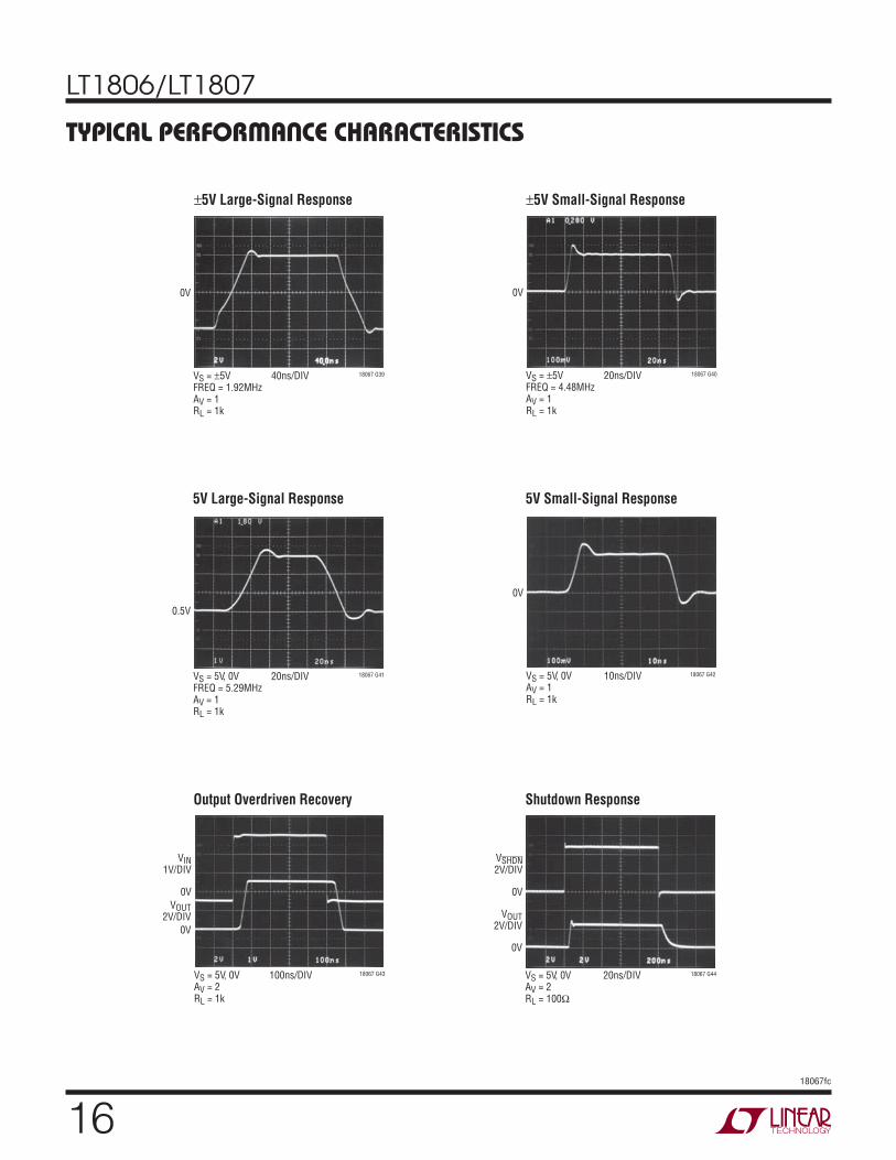
TYPICAL PERFORMANCE CHARACTERISTICS
40ns/DIV
0V
18067 G39 VS = 5VFREQ = 1.92MHzAV = 1RL = 1k
±5V Large-Signal Response
20ns/DIV 18067 G40
0V
VS = 5VFREQ = 4.48MHzAV = 1RL = 1k
±5V Small-Signal Response
20ns/DIV 18067 G41
0.5V
VS = 5V, 0VFREQ = 5.29MHzAV = 1RL = 1k
5V Large-Signal Response
10ns/DIV 18067 G42
0V
VS = 5V, 0VAV = 1RL = 1k
5V Small-Signal Response
100ns/DIV
0V
0V
VIN1V/DIV
18067 G43 VS = 5V, 0VAV = 2RL = 1k
VOUT2V/DIV
Output Overdriven Recovery
20ns/DIV 18067 G44
0V
0V
VSHDN2V/DIV
VS = 5V, 0VAV = 2RL = 100Ω
VOUT2V/DIV
Shutdown Response
LT1806/LT1807
1718067fc
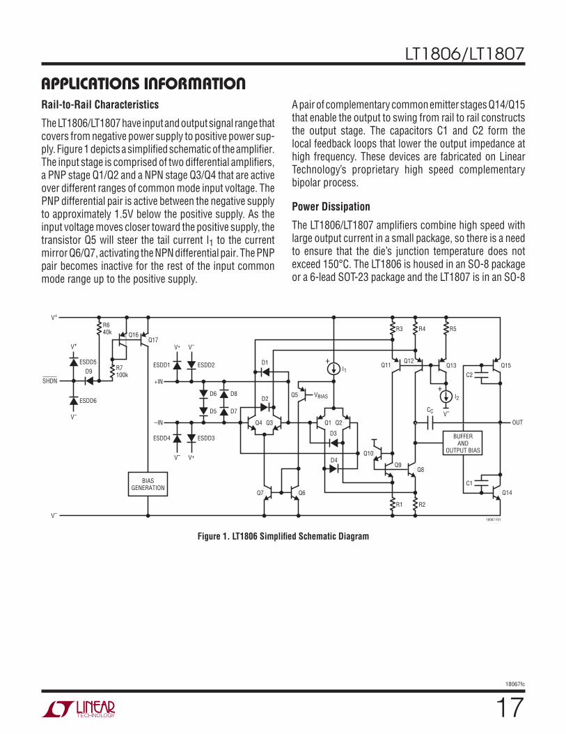
Rail-to-Rail Characteristics
The LT1806/LT1807 have input and output signal range that covers from negative power supply to positive power sup-ply. Figure 1 depicts a simplifi ed schematic of the amplifi er. The input stage is comprised of two differential amplifi ers, a PNP stage Q1/Q2 and a NPN stage Q3/Q4 that are active over different ranges of common mode input voltage. The PNP differential pair is active between the negative supply to approximately 1.5V below the positive supply. As the input voltage moves closer toward the positive supply, the transistor Q5 will steer the tail current I1 to the current mirror Q6/Q7, activating the NPN differential pair. The PNP pair becomes inactive for the rest of the input common mode range up to the positive supply.
APPLICATIONS INFORMATIONA pair of complementary common emitter stages Q14/Q15 that enable the output to swing from rail to rail constructs the output stage. The capacitors C1 and C2 form the local feedback loops that lower the output impedance at high frequency. These devices are fabricated on Linear Technology’s proprietary high speed complementary bipolar process.
Power Dissipation
The LT1806/LT1807 amplifi ers combine high speed with large output current in a small package, so there is a need to ensure that the die’s junction temperature does not exceed 150°C. The LT1806 is housed in an SO-8 package or a 6-lead SOT-23 package and the LT1807 is in an SO-8
Q4
Q6
Q3
Q7
Q10
Q1
Q13 Q15
OUTQ2
Q11Q12
Q9
Q5 VBIAS
I1
D2
D1
D5
D4
D3
D6
D7
D8
ESDD2ESDD1
+IN
–IN
V–
ESDD3ESDD4
V+
V+V–
Q8
R2R1
R3 R4 R5
Q14
18067 F01
+
I2
C2
CCV–
+
C1
BUFFERAND
OUTPUT BIAS
Q17Q16
ESDD5
SHDN
V+
V–
R7100k
R640k
D9
V+
V–
ESDD6
BIASGENERATION
Figure 1. LT1806 Simplifi ed Schematic Diagram
LT1806/LT1807
1818067fc
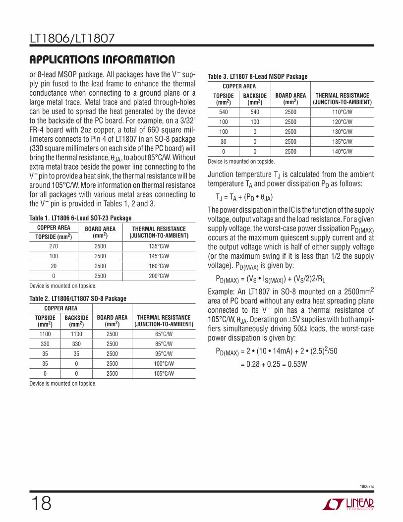
or 8-lead MSOP package. All packages have the V – sup-ply pin fused to the lead frame to enhance the thermal conductance when connecting to a ground plane or a large metal trace. Metal trace and plated through-holes can be used to spread the heat generated by the device to the backside of the PC board. For example, on a 3/32" FR-4 board with 2oz copper, a total of 660 square mil-limeters connects to Pin 4 of LT1807 in an SO-8 package (330 square millimeters on each side of the PC board) will bring the thermal resistance, θJA, to about 85°C/W. Without extra metal trace beside the power line connecting to the V – pin to provide a heat sink, the thermal resistance will be around 105°C/W. More information on thermal resistance for all packages with various metal areas connecting to the V – pin is provided in Tables 1, 2 and 3.
Table 1. LT1806 6-Lead SOT-23 Package
COPPER AREA BOARD AREA(mm2)
THERMAL RESISTANCE (JUNCTION-TO-AMBIENT) TOPSIDE (mm2)
270 2500 135°C/W
100 2500 145°C/W
20 2500 160°C/W
0 2500 200°C/W
Device is mounted on topside.
Table 2. LT1806/LT1807 SO-8 Package
COPPER AREA
BOARD AREA(mm2)
THERMAL RESISTANCE (JUNCTION-TO-AMBIENT)
TOPSIDE(mm2)
BACKSIDE(mm2)
1100 1100 2500 65°C/W
330 330 2500 85°C/W
35 35 2500 95°C/W
35 0 2500 100°C/W
0 0 2500 105°C/W
Device is mounted on topside.
APPLICATIONS INFORMATIONTable 3. LT1807 8-Lead MSOP Package
COPPER AREA
BOARD AREA(mm2)
THERMAL RESISTANCE (JUNCTION-TO-AMBIENT)
TOPSIDE(mm2)
BACKSIDE(mm2)
540 540 2500 110°C/W
100 100 2500 120°C/W
100 0 2500 130°C/W
30 0 2500 135°C/W
0 0 2500 140°C/W
Device is mounted on topside.
Junction temperature TJ is calculated from the ambient temperature TA and power dissipation PD as follows:
TJ = TA + (PD • θJA)
The power dissipation in the IC is the function of the supply voltage, output voltage and the load resistance. For a given supply voltage, the worst-case power dissipation PD(MAX) occurs at the maximum quiescent supply current and at the output voltage which is half of either supply voltage (or the maximum swing if it is less than 1/2 the supply voltage). PD(MAX) is given by:
PD(MAX) = (VS • IS(MAX)) + (VS/2)2/RL
Example: An LT1807 in SO-8 mounted on a 2500mm2 area of PC board without any extra heat spreading plane connected to its V – pin has a thermal resistance of 105°C/W, θJA. Operating on ±5V supplies with both ampli-fi ers simultaneously driving 50Ω loads, the worst-case power dissipation is given by:
PD(MAX) = 2 • (10 • 14mA) + 2 • (2.5)2/50
= 0.28 + 0.25 = 0.53W
LT1806/LT1807
1918067fc
APPLICATIONS INFORMATIONThe maximum ambient temperature that the part is allowed to operate is:
TA = TJ – (PD(MAX) • 105°C/W)
= 150°C – (0.53W • 105°C/W) = 94°C
To operate the device at higher ambient temperature, connect more metal area to the V – pin to reduce the thermal resistance of the package as indicated in Table 2.
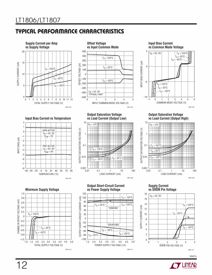
Input Offset Voltage
The offset voltage will change depending upon which input stage is active and the maximum offset voltage is guaranteed to less than 550μV. To maintain the precision characteristics of the amplifi er, the change of VOS over the entire input common mode range (CMRR) is limited to be less than 550μV on a single 5V and 3V supply.
Input Bias Current
The input bias current polarity depends on a given input common voltage at which the input stage is operating. When the PNP input stage is active, the input bias currents fl ow out of the input pins. When the NPN input stage is activated, the input bias current fl ows into the input pins. Because the input offset current is less than the input bias current, matching the source resistances at the input pins will reduce total offset error.
Output
The LT1806/LT1807 can deliver a large output current, so the short-circuit current limit is set around 85mA to prevent damage to the device. Attention must be paid to keep the junction temperature of the IC below the absolute maximum rating of 150°C (refer to the Power Dissipation section) when the output is continuously short circuited. The output of the amplifi er has reverse-biased diodes connected to each supply. If the output is forced beyond either supply, unlimited current will fl ow through these diodes. If the current is transient and limited to one hundred milliamps or less, no damage to the device will occur.
Overdrive Protection
When the input voltage exceeds the power supplies, two pairs of crossing diodes D1 to D4 will prevent the output from reversing polarity. If the input voltage exceeds either power supply by 700mV, diode D1/D2 or D3/D4 will turn on to keep the output at the proper polarity. For the phase reversal protection to perform properly, the input current must be limited to less than 5mA. If the amplifi er is severely overdriven, an external resistor should be used to limit the overdrive current.
LT1806/LT1807
2018067fc
APPLICATIONS INFORMATIONThe LT1806/LT1807’s input stages are also protected against large differential input voltages of 1.4V or higher by a pair of back-to-back diodes, D5/D8, that prevent the emitter-base breakdown of the input transistors. The current in these diodes should be limited to less than 10mA when they are active. The worst-case differential input voltage usually occurs when the input is driven while the output is shorted to ground in a unity gain confi guration. In addition, the amplifi er is protected against ESD strikes up to 3kV on all pins by a pair of protection diodes, ESDD1 to ESDD6, on each pin that are connected to the power supplies as shown in Figure 1.
Capacitive Load
The LT1806/LT1807 are optimized for high bandwidth and low distortion applications. They can drive a capacitive load of about 20pF in a unity-gain confi guration, and more for higher gain. When driving a larger capacitive load, a resistor of 10Ω to 50Ω should be connected between the output and the capacitive load to avoid ringing or oscilla-tion. The feedback should still be taken from the output so that the resistor will isolate the capacitive load to ensure stability. Graphs on capacitive loads indicate the transient response of the amplifi er when driving the capacitive load with a specifi ed series resistor.
Feedback Components
When feedback resistors are used to set up gain, care must be taken to ensure that the pole formed by the feedback resistors and the total capacitance at the inverting input does not degrade stability. For instance, the LT1806/LT1807 in a noninverting gain of 2, set up with two 1k resistors and a capacitance of 3pF (part plus PC board) will probably ring in transient response. The pole is formed at 106MHz that will reduce phase margin by 34 degrees when the crossover frequency of the amplifi er is around 70MHz. A capacitor of 3pF or higher connected across the feedback resistor will eliminate any ringing or oscillation.
SHDN Pin
The LT1806 has a SHDN pin to reduce the supply current to less than 0.9mA. When the SHDN pin is pulled low, it will generate a signal to power down the device. If the pin is left unconnected, an internal pull-up resistor of 40k will keep the part fully operating as shown in Figure 1. The output will be high impedance during shutdown, and the turn-on and turn-off time is less than 100ns. Because the input is protected by a pair of back-to-back diodes, the input signal will feed through to the output during shutdown mode if the amplitude of signal between the inputs is larger than 1.4V.
LT1806/LT1807
2118067fc
TYPICAL APPLICATIONSDriving A/D Converter
The LT1806/LT1807 have 60ns settling time to 0.01% on a 2V step signal, and 20Ω output impedance at 100MHz, that makes them ideal for driving high speed A/D convert-ers. With the rail-to-rail input and output, and low supply voltage operation, the LT1806/LT1807 are also desirable for single supply applications. As shown in the application on the front page of this data sheet, the LT1807 drives a 10Msps, 12-bit, LTC1420 ADC in a gain of 20. Driving the LTC1420 differentially will optimize the signal-to-noise ratio, SNR, and the total harmonic distortion, THD, of the A/D converter. The lowpass fi lter, R5, R6 and C3 reduce
noise or distortion products that might come from the input signal. High quality capacitors and resistors, NPO chip capacitor and metal fi lm surface mount resistors, should be used since these components can add to distortion. The voltage glitch of the converter, due to its sampling nature is buffered by the LT1807, and the ability of the amplifi er to settle it quickly will affect the spurious free dynamic range of the system. Figure 2 depicts the LT1806 driving LTC1420 at noninverting gain of 2 confi guration. The FFT responses show a better than 92dB of spurious free dynamic range, SFDR.
Figure 2. Noninverting A/D Driver
–
+
LT1806LTC1420
PGA GAIN = 1REF = 2.048V
5V
5V
12 BITS10Msps
–5V
–5V
•••
R21k
R11k
VIN1.5VP-P
C1470pF
–AIN
18067 F02
+AIN
R349.9Ω
Figure 3. 4096 Point FFT Response
FREQUENCY (MHz)
0–120
AM
PLIT
UD
E (
dB
)
–100
–80
–60
–40
–20
0
1 2 3 4
18067 F03
5
VS = 5VAV = 2fSAMPLE = 10MspsfIN = 1.4086MHzSFDR = 92.5dB
LT1806/LT1807
2218067fc
TYPICAL APPLICATIONSSingle Supply Video Line Driver
The LT1806/LT1807 are wideband rail-to-rail op amps with large output current that allows them to drive video signals in low supply applications. Figure 4 depicts a single supply video line driver with AC coupling to minimize the quies-cent power dissipation. Resistors R1 and R2 are used to level-shift the input and output to provide the largest signal swing. The gain of 2 is set up with R3 and R4 to restore the signal at VOUT, which is attenuated by 6dB due to the matching of the 75Ω line with the back-terminated resistor,
R5. The back termination will eliminate any refl ection of the signal that comes from the load. The input termination resistor, RT, is optional—it is used only if matching of the incoming line is necessary. The values of C1, C2 and C3 are selected to minimize the droop of the luminance signal. In some less stringent requirements, the value of capacitors could be reduced. The –3dB bandwidth of the driver is about 90MHz on 5V supply, and the amount of peaking will vary upon the value of capacitor C4.
Figure 4. 5V Single Supply Video Line Driver
–
+
LT1806
VIN
18067 F04
C133μF
C2150μF
RT75Ω
RLOAD75Ω
VOUTR25k
R31k
R41k
C43pF
R15k
5V
2
3
6
7
4
R575Ω
75WCOAX CABLE
C31000μF
+
+
+
Figure 5. Video Line Driver Frequency Response
FREQUENCY (MHz)
–2VO
LTA
GE G
AIN
(dB
)
4
5
–3
–4
3
0
2
1
–1
0.2 10 100
18067 F05
–51
VS = 5V, 0V
LT1806/LT1807
2318067fc
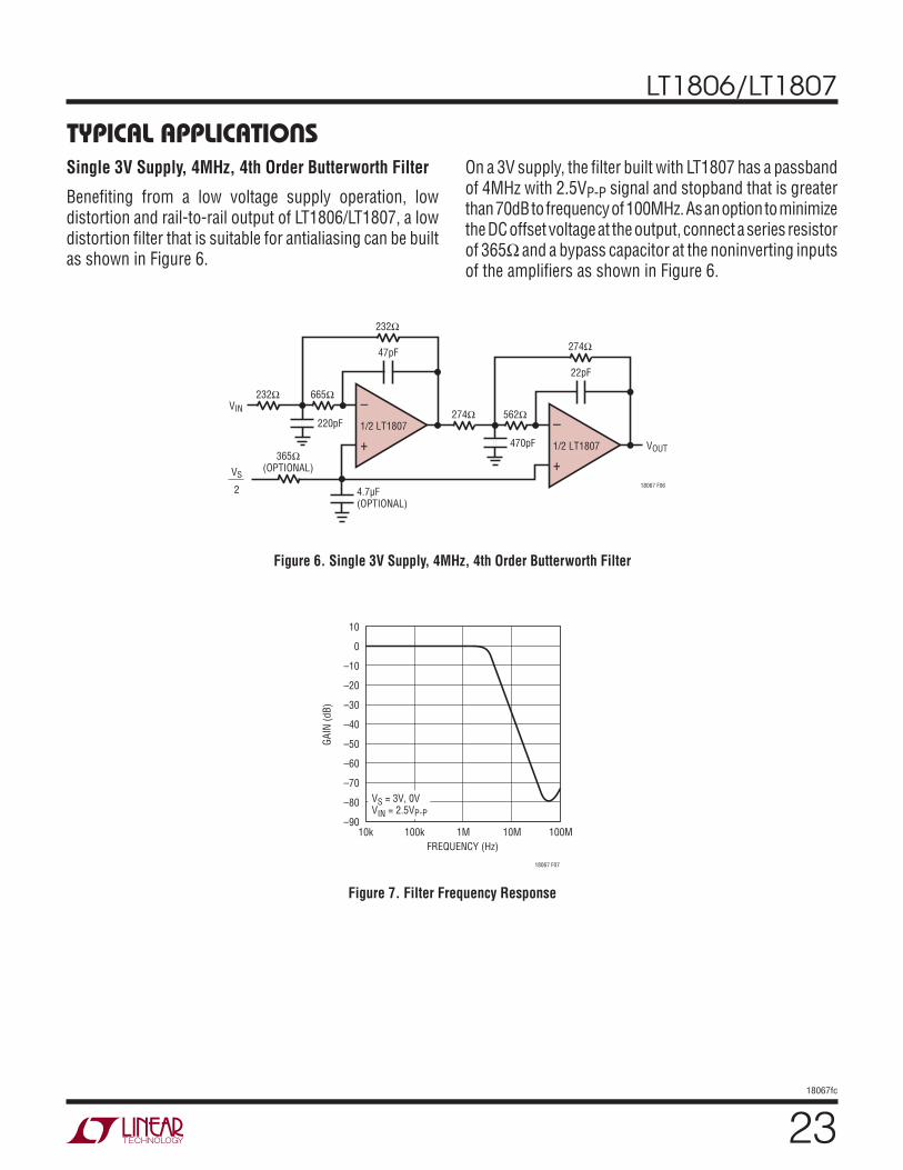
TYPICAL APPLICATIONSSingle 3V Supply, 4MHz, 4th Order Butterworth Filter
Benefi ting from a low voltage supply operation, low distortion and rail-to-rail output of LT1806/LT1807, a low distortion fi lter that is suitable for antialiasing can be built as shown in Figure 6.
On a 3V supply, the fi lter built with LT1807 has a passband of 4MHz with 2.5VP-P signal and stopband that is greater than 70dB to frequency of 100MHz. As an option to minimize the DC offset voltage at the output, connect a series resistor of 365Ω and a bypass capacitor at the noninverting inputs of the amplifi ers as shown in Figure 6.
Figure 6. Single 3V Supply, 4MHz, 4th Order Butterworth Filter
+
–
VS
2
47pF
1/2 LT1807220pF
665ΩVIN
VOUT
18067 F06
365Ω(OPTIONAL)
232Ω
232Ω
4.7μF(OPTIONAL)
+
–
22pF
470pF
562Ω274Ω
274Ω
1/2 LT1807
Figure 7. Filter Frequency Response
FREQUENCY (Hz)
10k 100k 1M 10M 100M
GA
IN (
dB
)
18067 F07
10
0
–10
–20
–30
–40
–50
–60
–70
–80
–90
VS = 3V, 0VVIN = 2.5VP-P
LT1806/LT1807
2418067fc
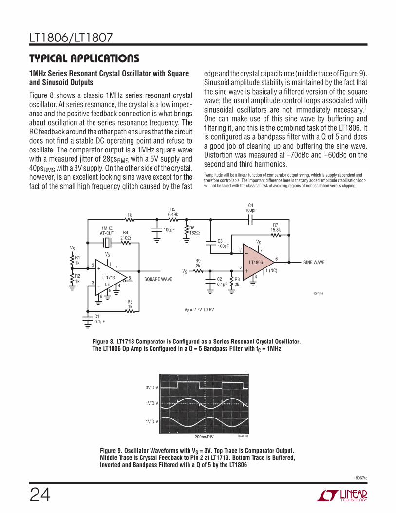
TYPICAL APPLICATIONS1MHz Series Resonant Crystal Oscillator with Square and Sinusoid Outputs
Figure 8 shows a classic 1MHz series resonant crystal oscillator. At series resonance, the crystal is a low imped-ance and the positive feedback connection is what brings about oscillation at the series resonance frequency. The RC feedback around the other path ensures that the circuit does not fi nd a stable DC operating point and refuse to oscillate. The comparator output is a 1MHz square wave with a measured jitter of 28psRMS with a 5V supply and 40psRMS with a 3V supply. On the other side of the crystal, however, is an excellent looking sine wave except for the fact of the small high frequency glitch caused by the fast
edge and the crystal capacitance (middle trace of Figure 9). Sinusoid amplitude stability is maintained by the fact that the sine wave is basically a fi ltered version of the square wave; the usual amplitude control loops associated with sinusoidal oscillators are not immediately necessary.1 One can make use of this sine wave by buffering and fi ltering it, and this is the combined task of the LT1806. It is confi gured as a bandpass fi lter with a Q of 5 and does a good job of cleaning up and buffering the sine wave. Distortion was measured at –70dBc and –60dBc on the second and third harmonics.
Figure 8. LT1713 Comparator is Confi gured as a Series Resonant Crystal Oscillator. The LT1806 Op Amp is Confi gured in a Q = 5 Bandpass Filter with fC = 1MHz
–
+
8 SQUARE WAVE
VS
VS
VS
17
45
R31k
R4210Ω
R11k
R82k
R92k
R56.49k1k
R715.8k
R21k
1MHZAT-CUT
C10.1μF
6
3
2
C20.1μF
C4100pF
C3100pF
LT1713
–
+
VS
7
6
1 (NC)
4
18067 F08
VS = 2.7V TO 6V
3
2
LT1806
LE
R6162Ω
100pF
SINE WAVE
200ns/DIV
1V/DIV
1V/DIV
3V/DIV
18067 F09
1Amplitude will be a linear function of comparator output swing, which is supply dependent and therefore controllable. The important difference here is that any added amplitude stabilization loop will not be faced with the classical task of avoiding regions of nonoscillation versus clipping.
Figure 9. Oscillator Waveforms with VS = 3V. Top Trace is Comparator Output. Middle Trace is Crystal Feedback to Pin 2 at LT1713. Bottom Trace is Buffered, Inverted and Bandpass Filtered with a Q of 5 by the LT1806
LT1806/LT1807
2518067fc
PACKAGE DESCRIPTION
1.50 – 1.75(NOTE 4)
2.80 BSC
0.30 – 0.45 6 PLCS (NOTE 3)
DATUM ‘A’
0.09 – 0.20(NOTE 3) S6 TSOT-23 0302 REV B
2.90 BSC(NOTE 4)
0.95 BSC
1.90 BSC
0.80 – 0.90
1.00 MAX0.01 – 0.10
0.20 BSC
0.30 – 0.50 REF
PIN ONE ID
NOTE:1. DIMENSIONS ARE IN MILLIMETERS2. DRAWING NOT TO SCALE3. DIMENSIONS ARE INCLUSIVE OF PLATING4. DIMENSIONS ARE EXCLUSIVE OF MOLD FLASH AND METAL BURR5. MOLD FLASH SHALL NOT EXCEED 0.254mm6. JEDEC PACKAGE REFERENCE IS MO-193
3.85 MAX
0.62MAX
0.95REF
RECOMMENDED SOLDER PAD LAYOUTPER IPC CALCULATOR
1.4 MIN2.62 REF
1.22 REF
S6 Package6-Lead Plastic TSOT-23
(Reference LTC DWG # 05-08-1636)
LT1806/LT1807
2618067fc
MSOP (MS8) 0307 REV F
0.53 0.152
(.021 .006)
SEATINGPLANE
NOTE:1. DIMENSIONS IN MILLIMETER/(INCH)2. DRAWING NOT TO SCALE3. DIMENSION DOES NOT INCLUDE MOLD FLASH, PROTRUSIONS OR GATE BURRS. MOLD FLASH, PROTRUSIONS OR GATE BURRS SHALL NOT EXCEED 0.152mm (.006") PER SIDE4. DIMENSION DOES NOT INCLUDE INTERLEAD FLASH OR PROTRUSIONS. INTERLEAD FLASH OR PROTRUSIONS SHALL NOT EXCEED 0.152mm (.006") PER SIDE5. LEAD COPLANARITY (BOTTOM OF LEADS AFTER FORMING) SHALL BE 0.102mm (.004") MAX
0.18
(.007)
0.254
(.010)
1.10
(.043)MAX
0.22 – 0.38
(.009 – .015)TYP
0.1016 0.0508
(.004 .002)
0.86
(.034)REF
0.65
(.0256)BSC
0 – 6 TYP
DETAIL “A”
DETAIL “A”
GAUGE PLANE
1 2 3 4
4.90 0.152
(.193 .006)
8 7 6 5
3.00 0.102
(.118 .004)
(NOTE 3)
3.00 0.102
(.118 .004)
(NOTE 4)
0.52
(.0205)REF
5.23(.206)MIN
3.20 – 3.45(.126 – .136)
0.889 0.127(.035 .005)
RECOMMENDED SOLDER PAD LAYOUT
0.42 0.038(.0165 .0015)
TYP
0.65(.0256)
BSC
PACKAGE DESCRIPTIONMS8 Package
8-Lead Plastic MSOP(Reference LTC DWG # 05-08-1660 Rev F)
LT1806/LT1807
2718067fc
Information furnished by Linear Technology Corporation is believed to be accurate and reliable. However, no responsibility is assumed for its use. Linear Technology Corporation makes no representa-tion that the interconnection of its circuits as described herein will not infringe on existing patent rights.
PACKAGE DESCRIPTIONS8 Package
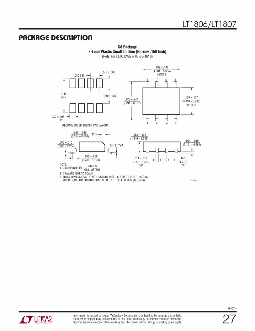
8-Lead Plastic Small Outline (Narrow .150 Inch)(Reference LTC DWG # 05-08-1610)
.016 – .050(0.406 – 1.270)
.010 – .020(0.254 – 0.508)
45
0 – 8 TYP.008 – .010
(0.203 – 0.254)
SO8 0303
.053 – .069(1.346 – 1.752)
.014 – .019(0.355 – 0.483)
TYP
.004 – .010(0.101 – 0.254)
.050(1.270)
BSC
1 2 3 4
.150 – .157(3.810 – 3.988)
NOTE 3
8 7 6 5
.189 – .197(4.801 – 5.004)
NOTE 3
.228 – .244(5.791 – 6.197)
.245MIN .160 .005
RECOMMENDED SOLDER PAD LAYOUT
.045 .005.050 BSC
.030 .005 TYP
INCHES(MILLIMETERS)
NOTE:1. DIMENSIONS IN
2. DRAWING NOT TO SCALE3. THESE DIMENSIONS DO NOT INCLUDE MOLD FLASH OR PROTRUSIONS. MOLD FLASH OR PROTRUSIONS SHALL NOT EXCEED .006" (0.15mm)
LT1806/LT1807
2818067fc
Linear Technology Corporation1630 McCarthy Blvd., Milpitas, CA 95035-7417 (408) 432-1900 ● FAX: (408) 434-0507 ● www.linear.com © LINEAR TECHNOLOGY CORPORATION 2000
LT 0809 REV C • PRINTED IN USA
RELATED PARTSPART NUMBER DESCRIPTION COMMENTS
LT1395 400MHz Current Feedback Amplifi er 800V/μs Slew Rate, Shutdown
LT1399 Triple 300MHz Current Feedback Amplifi er 0.1dB Gain Flatness to 150MHz, Shutdown
LT1632/LT1633 Dual/Quad 45MHz, 45V/μs Rail-to-Rail Input and Output Amplifi ers High DC Accuracy 1.35mV VOS(MAX), 70mA Output Current,Max Supply Current 5.2mA/Amp
LT1809/LT1810 Single/Dual 180MHz Input and Output Rail-to-Rail Amplifi ers 350V/μs Slew Rate, Shutdown, Low Distortion –90dBc at 5MHz
LT1812/LT1813 3mA, 100MHz, 750V/μs Op Amp High Slew Rate
LT1818/LT1819 9mA, 400MHz, 2500V/μs Op Amp Ultrahigh Slew Rate
LT6200/LT6201 165MHz Rail-to-Rail Input and Output, 0.95nV/√Hz Low Noise Op Amp
Lowest Noise
LT6202/LT6203 100MHz Rail-to-Rail Input and Output, 1.9nV/√Hz Op Amp ICC = 2.5mA
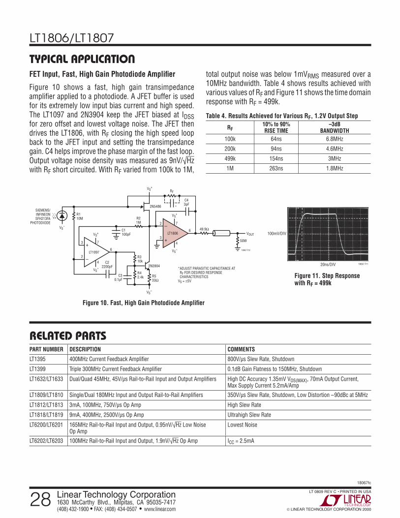
TYPICAL APPLICATIONFET Input, Fast, High Gain Photodiode Amplifi er
Figure 10 shows a fast, high gain transimpedance amplifi er applied to a photodiode. A JFET buffer is used for its extremely low input bias current and high speed. The LT1097 and 2N3904 keep the JFET biased at IDSS for zero offset and lowest voltage noise. The JFET then drives the LT1806, with RF closing the high speed loop back to the JFET input and setting the transimpedance gain. C4 helps improve the phase margin of the fast loop. Output voltage noise density was measured as 9nV/√Hz
with RF short circuited. With RF varied from 100k to 1M,
total output noise was below 1mVRMS measured over a 10MHz bandwidth. Table 4 shows results achieved with various values of RF and Figure 11 shows the time domain response with RF = 499k.
Table 4. Results Achieved for Various RF, 1.2V Output Step
RF10% to 90%RISE TIME
–3dBBANDWIDTH
100k 64ns 6.8MHz
200k 94ns 4.6MHz
499k 154ns 3MHz
1M 263ns 1.8MHz
Figure 10. Fast, High Gain Photodiode Amplifi er
–
+
R310k
R110M
SIEMENS/INFINEONSFH213FA
PHOTODIODE
R21M
RF
49.9Ω
50W
18067 F10
R533Ω
R42.4k
3
6
4
7
VS+
VS–
VS–
2
C22200pF
C30.1μF
C1100pF
C43pF
LT1097
–
+
2
6
4
7
VOUT
*2N5486
VS+
VS+
VS–
VS–
3LT1806
2N3904*ADJUST PARASITIC CAPACITANCE AT RF FOR DESIRED RESPONSE CHARACTERISTICSVS = 5V
Figure 11. Step Response with RF = 499k
20ns/DIV
100mV/DIV
18067 F11